Embed Size (px)
Citation preview
Student Presentation
High-Speed Circuits & Systems Lab.
Joungwook Moon
2013. 05. 27
About Paper
2

Contents
1. Introduction
2. Noise transfer function- Classical analysis- Discussion
3. Design of PLL and sub -blocks
4. Measurement result
5. Conclusion

A self-calibration concept applied to an frequencysynthesizer
Designing a low-noise frequency synthesizer while not compromising the frequency range
Shows noise generation, accumulation, and filteringwithin a PLL
Introduction
4
Contents
1. Introduction
2. Noise transfer function- Classical analysis- Discussion
3. Design of PLL and sub -blocks
4. Measurement result
5. Conclusion

Noise transfer functions in PLLs
A. Classical analysis of a closed-loop PLL
2
(1 )( )( )( )
d o
o
d o d oi
K K sRCs CH s N
K K K Ks s s RCC C
closed-loop transfer function2
2 2
2( )2
n n
n n
sH s Ns s
d on
K KC
2 d oR K K C
Low pass filter for input noise6

Noise transfer functions in PLLs
B. Transfer functions for various equivalent noise source
2 2
(1 )( )( )( ) 2
o
oi
n n n
K sRCs CH s
i s s s
2 2
( )( )( ) 2
o ov
n n n
s sKH sv s s s
2
2 2
( )( )( ) 2
o
n n n
s sH ss s s
(1) (2)
(3)
7
(1) (2) (3)
Low-pass filter Band-pass filter
High-pass filter

Noise transfer functions in PLLsInput Noise PFD/CP Noise
Loop-filter Noise VCO Noise
8
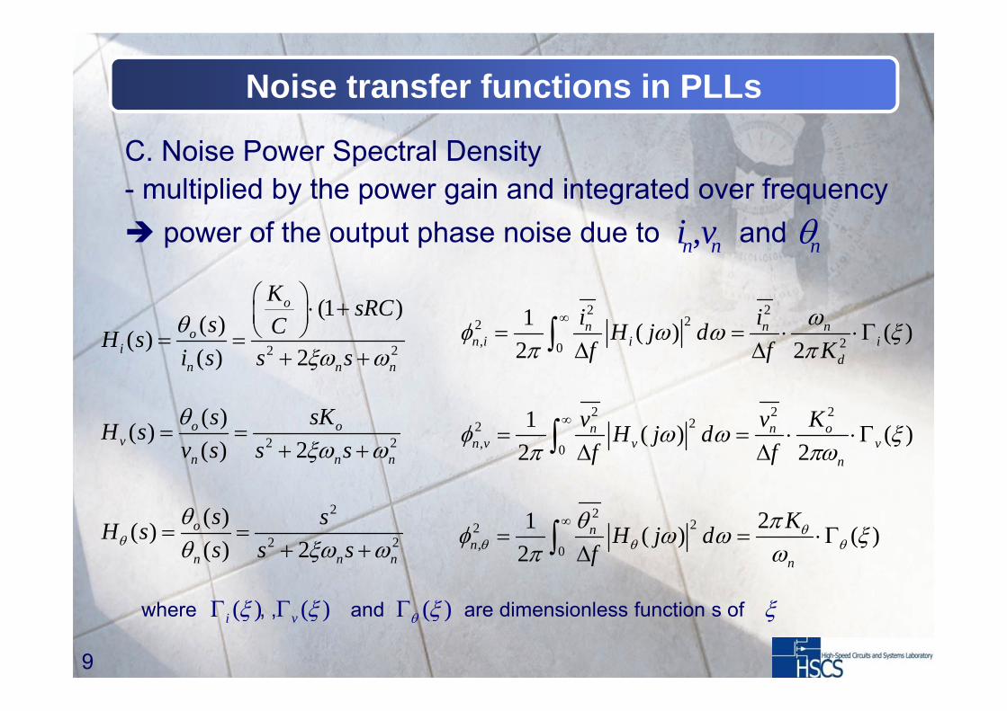
Noise transfer functions in PLLs
C. Noise Power Spectral Density- multiplied by the power gain and integrated over frequency
2 2
(1 )( )( )( ) 2
o
oi
n n n
K sRCs CH s
i s s s
2 2
( )( )( ) 2
o ov
n n n
s sKH sv s s s
2
2 2
( )( )( ) 2
o
n n n
s sH ss s s
2 222
, 20
1 ( ) ( )2 2
n n nn i i i
d
i iH j df f K
2 2 222
, 0
1 ( ) ( )2 2
n n on v v v
n
v v KH j df f
222
, 0
21 ( ) ( )2
nn
n
KH j df
power of the output phase noise due to and ,n ni v n
where , , and are dimensionless function s of( )i ( )v ( )
9
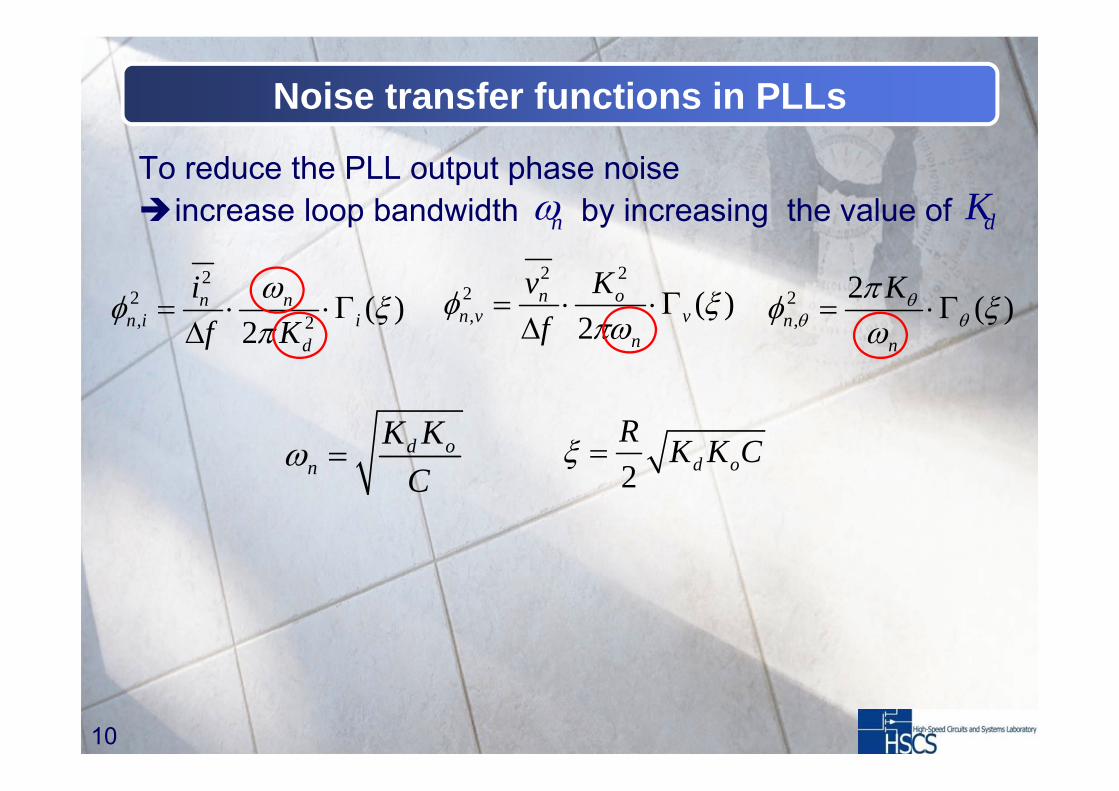
Noise transfer functions in PLLs
To reduce the PLL output phase noiseincrease loop bandwidth by increasing the value of
22, 2 ( )
2n n
n i id
if K
2 22, ( )
2n o
n v vn
v Kf
2,
2 ( )nn
K
dKn
d on
K KC
2 d oR K K C
10

Noise transfer functions in PLLs
To reduce the PLL output phase noiseincrease loop bandwidth by increasing the value of dKn
Max. loop bandwidth is restricted by the update rate of the PD1/10 of the phase detector update rate to avoid instability
22, 2 ( )
2n n
n i id
if K
2 22, ( )
2n o
n v vn
v Kf
2,
2 ( )nn
K
• Once the loop bandwidth is fixed, • Kd has to be balanced with Ko
• Reduction Ko less sensitive VCO @ control port (eq. 2)(Ko not affect the noise generated within the oscillator (eq. 3))
11
Contents
1. Introduction
2. Noise transfer function- Classical analysis- Discussion
3. Design of PLL and sub-blocks
4. Measurement result
5. Conclusion

Design strategy of Frequency Synthesizer
1. Large frequency tuning range is required
2. VCO has to operate with a wide range
3. Loop bandwidth is maximized for reducing the phase noise due to internal source of the PLL
4. Increasing Kd with lowering Ko for constant loop bandwidth
13
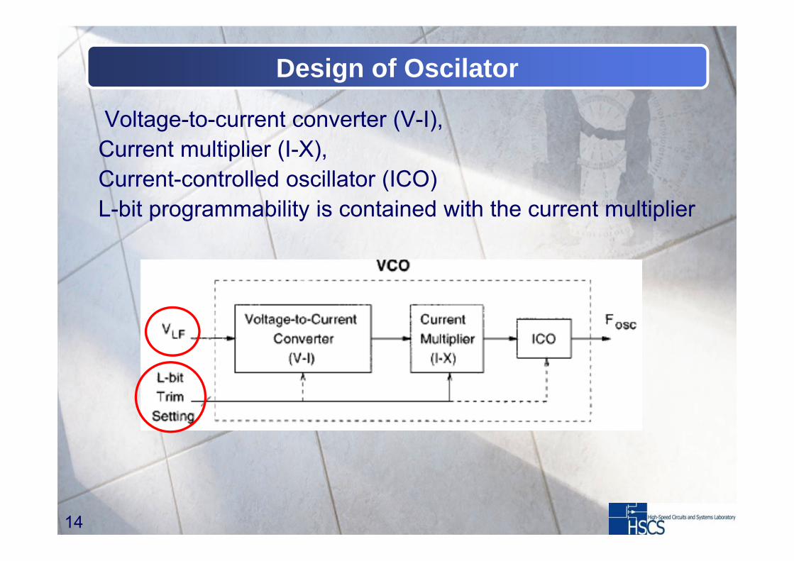
Design of Oscilator
Voltage-to-current converter (V-I), Current multiplier (I-X),Current-controlled oscillator (ICO)L-bit programmability is contained with the current multiplier
14
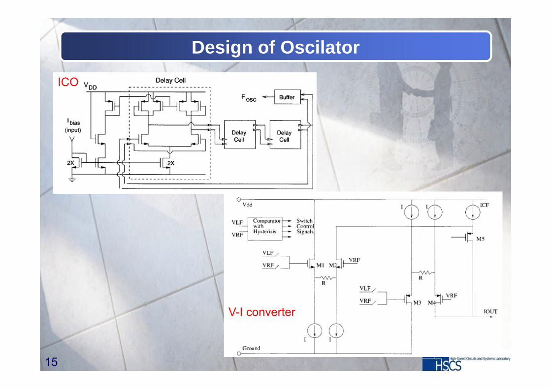
Design of Oscilator
ICO
V-I converter
15

Input control voltage to output frequency transfer function issmall enough for low sensitivity to noise
Measured transfer function of the overall VCO
Design of Oscilator
16

Design of PLL
Two parallel paths from the PFDOutput of the self-calibration circuit control the VCO
1. At power up, SW1 off, SW2 on. reset/calibrate signal on2. Start calibration, find optimum L-bit value (algorithm)3. Fix calibration value. SW1 on, SW2 off. 4. Running normal PLL operation
17
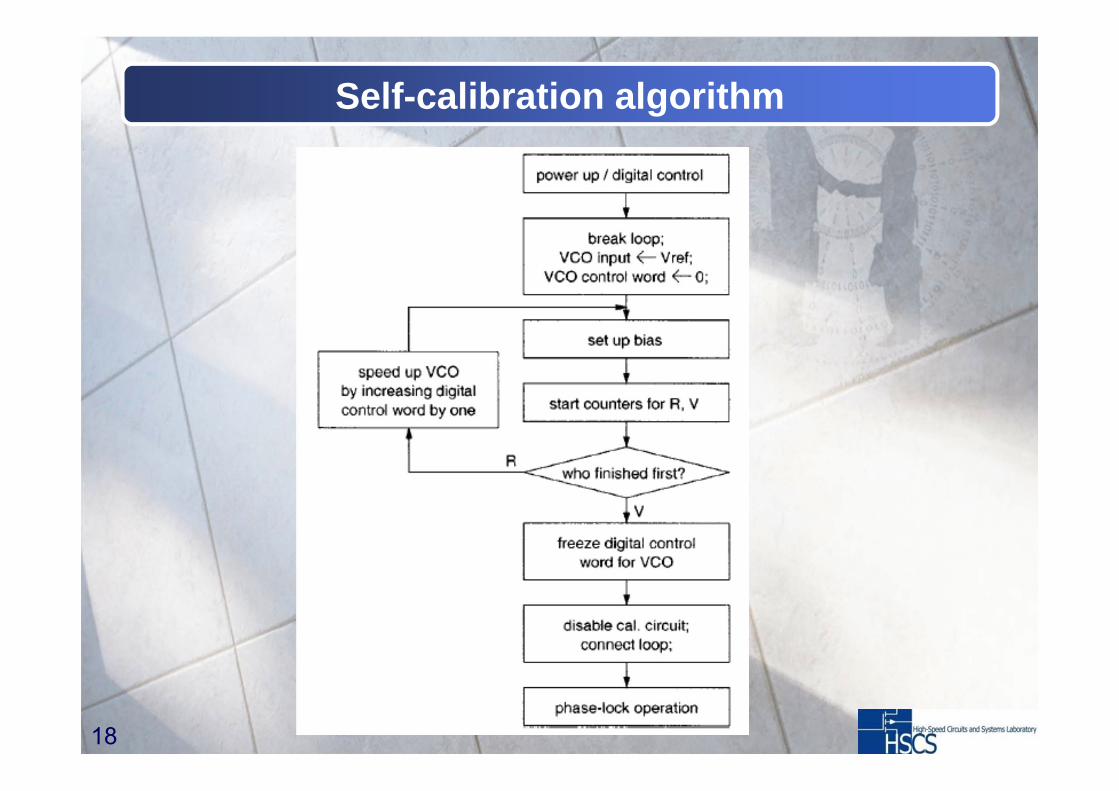
Self-calibration algorithm
18
Contents
1. Introduction
2. Noise transfer function- Classical analysis- Discussion
3. Design of PLL and sub -blocks
4. Measurement result
5. Conclusion

Measurement Result
• 0.35-μm 3-V digital CMOS technology• Operating range : 80 MHz ~ 1 GHz• 3-dB loop bandwidth : 420 kHz• RMS Jitter : 26.8 ps @ 560 MHz
20
Measurement Result
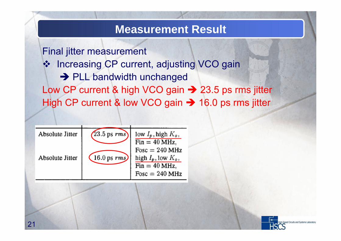
Final jitter measurement Increasing CP current, adjusting VCO gain PLL bandwidth unchanged
Low CP current & high VCO gain 23.5 ps rms jitterHigh CP current & low VCO gain 16.0 ps rms jitter
21
Conclusion
0.35-μm 3-V digital CMOS technology
Automatic self-calibration VCO is used for lower Ko
PLL jitter is dominated by internal device noise, the amount of jitter reduction from self-calibrationof the VCO is significant
22

Thank you
Q & A

APPENDIX
http://en.wikipedia.org/wiki/Jitter


![Silicon optical Modulator [호환 모드] - Yonsei Universitytera.yonsei.ac.kr/class/2014_1_2/lecture/Silicon optical... · 2014-04-29 · High-Speed Circuits & Systems Lab. Dept](https://img.dokumen.tips/doc/110x75/5e47b83971b5a12fea2e9c32/silicon-optical-modulator-eeoe-yonsei-optical-2014-04-29-high-speed.jpg)