Embed Size (px)
Citation preview
7/5/09 11 1
Status and prospects of integrated nanophotonics circuits
Lars Thylén
Dept of Microelectronics and Applied Physics
Royal Institute of Technology (KTH) and Kista Photonics Research Center Stockholm, Sweden
Joint Research Center of Photonics of the Royal Institute of Technology and
Zhejiang University, Hangzhou, PR China
Information and Quantum Systems Laboratory HP Laboratories, Palo Alto, US

7/5/09 22 2
Acknowledgements
• Alexander Bratkovsky, HP Labs • Petter Holmström , KTH. • Dr Lech Wosinski, KTH • Ekaterina Ponizovskaya, HP Labs • Prof Connie Chang-Hasnain, UC Berkeley • PhD student Devang Parekh, UC Berkeley • Prof Ivan Kaminow, UC Berkeley • Prof Ken Gustafson, UC Berkeley • Prof Kevin Webb, Purdue Univ • Dr Y. Fu, KTH • Prof Hans Ågren, KTH • Dr SY Wang, HP Labs • Dr Jingjing Li, HP Labs • Prof Sailing He, Zhejiang U & KTH • Assoc Prof Min Qiu, KTH • Assoc Prof Eilert Berglind, KTH • Dr Min Yan, KTH • Dr Liu Liu, Ghent U • Assoc Prof Urban Westergren, KTH • Dr PY Fonjallaz, Kista Photonics Research Center • PhD student Yingran He, Zhejiang U • …….

7/5/09 33
Outline • Integrated photonics:
– Developments over the years and a ”Moore’s” law for integrated photonics
– Further progress?
• Nanophotonics and plasmonics: – Basic principles, waveguide properties – Performance limitations due to dissipative losses in passive
circuits*
• High optical confinement waveguides and photonic circuits • Metamaterials, what and why?
• Loss compensating gain, quantum dots and power dissipation in active circuits
• Conclusions * Note: There are numerous applications of plasmonics where optical losses are not
so important , e g sensors and SERS (Surface enhanced Raman scattering)
3

7/5/09 44
Integrated photonics
4

7/5/09 55
Vision in the mid 70s when the term Integrated optics was coined..
Δn k0 L=π
5

7/5/09 66 6
State - of- the Art Photonic IC (U of Eindhoven) Optical Cross-connect: 100’ish components
State-of the Art Electronic IC (Intel Website) Pentium 4: 42 M Transistors
Photonics is far behind electronics in maturity, But excellent research and business opportunities!
After ~30 years of development ....

7/5/09 77
“Moore´s law” for photonic light wave circuits
7
• Moore´s law for electronic ICs pertains to circuits with generic elements (transistors, resistors, capacitors), some fraction of which are active
• “Moore´s law” for PLCs: – No generic elements like in electronics but lots of different active and
passive device structures with different functions, in different materials. (hence transform PLCs to some “equivalent elements”)
– Assess Integration density for PLCs rather than total number of elements in our “Moore´s law”

7/5/09 88 8
-25
-20
-15
-10
-5
0
1985 1990 1995 2000 2005 2010
Years
2L
og
(#o
f d
ev
ice
s/ m
2)
A Moore´s law for integration density in terms of equivalent number of elements per square micron of integrated photonics devices:
Growing faster than the IC Moore´s law!
factor of 2/year
J. Zhejiang Univ SCIENCE 2006 7(12) p.1961-1964 http://www.zju.edu.cn/jzus/

7/5/09 99
Total minimum field width vs core width, planar waveguide, wavelength =1.55 mm
(core index, cladding index)
9
• Silica waveguide (1.5,1.4) 3 mm
• III V (3.4,3.1) 1 mm
• Silicon/air (3.5,1) appr 400 nm

7/5/09

7/5/09 1111
So how continue increasing integration density? Or
What comes after Si?
11
• Photonic crystals? – But wavelength sized waveguides and resonators…
• High refractive index? – But have to beat e g Si…
• Metals or negative epsilon materials? – Losses…
• ??

7/5/09 1212
What will integrated nanophotonics circuits bring (for telecom and interconnect)?
The classical issues for integrated photonics
• Insertion loss
• Polarization sensitivity
• Drive power
• Interfacing
• Functionality
• Footprint
• Power dissipation
• Cost
7/5/09 1313
13
Nanophotonic integrated circuits based on negative e materials
(plasmonic or metal optics) for high density lateral and
longitudinal device integration

7/5/09 1414
PLASMONICS …to be the key nanotechnology
that will combine electronic and photonic components on the same chip…
• Optical frequency subwavelength metallic wired circuits with propagation loss comparable to conventional optical waveguides;
• Highly efficient plasmonic LEDs with tunable radiation properties;
• Active control of plasmonic signals by electro-optic, all-optical, and piezoelectric modulation and gain mechanisms to plasmonic structures;
• 2D plasmonic optical components for coupling single mode fiber directly to plasmonic circuits;
• Deep subwavelength plasmonic nanolithography over large surfaces.
• Subwavelength imaging
Ekmel Ozbay, SCIENCE VOL 311 13 JANUARY 2006
7/5/09 1515
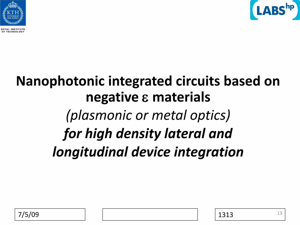
Dispersion equation for TM surface waves (TM-1)
15
Wave equation and continuity of Ez gives:
x
z
1m
m
m
e
zjxAH zxmy expexp zjxAH zxdy expexp
0
1
0
d
d
m
e
m
xm
d
xd
e
e
22
0
2
zdxd k e
22
0
2
zmxm k e
dm
mm
dm
dxd
effdm
dmz
k
k
k
ee
e
ee
e
ee
ee
22
0
2
22
0
2
22
0
2 )2
(
Also called Surface Plasmon Polariton

7/5/09 1616 16
200 300 400 500 600 700 800 900 10000
5
10
15
20
25
30
35
40
45
Wavelength (nm)
e"
Si
GaAs
Au
Ag
200 300 400 500 600 700 800 900 1000-60
-40
-20
0
20
40
60
Wavelength (nm)
e'
Si
GaAsGaAsGaAsGaAs
SiO2
Au
Ag
Real and imginary parts of epsilon of some metals
and semiconducors
!! e

7/5/09
• Trade off between optical confinement and photon life time (and Q)
• Group velocity converts photon lifetime to propagation distance
1717
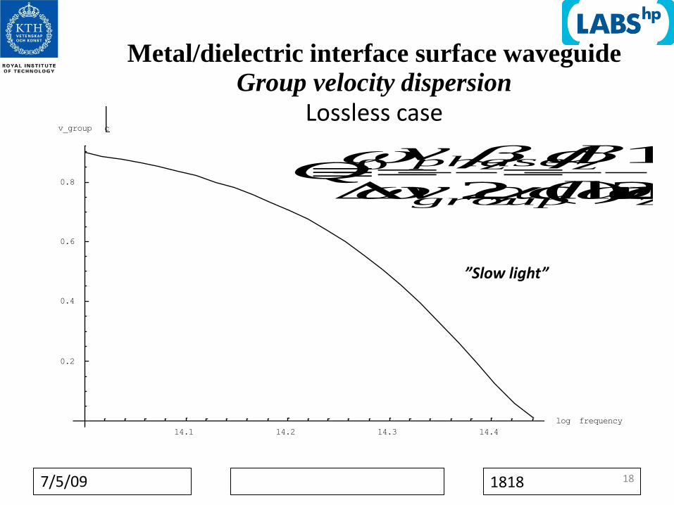
7/5/09 1818 18
14.1 14.2 14.3 14.4
log frequency
0.2
0.4
0.6
0.8
v_group c
Metal/dielectric interface surface waveguide Group velocity dispersion
Lossless case
z
z
z
z
group
phase
d
d
v
vQ
2
1
)(ln2
0
”Slow light”

7/5/09

7/5/09
7/5/09 2121
Examples of ultra compact waveguides and a suggested
roadmap for integrated optics devices
21

7/5/09 2222
Fabrication and Characterization of sub-wavelength structures
The top view of the structure
Schematics (a) and |Ex | mode profile (b) of the metal slot waveguide with a 150-nm-wide silicon core.
L. Chen, J. Shakya, and M. Lipson, "Subwavelength confinement in an integrated metal slot waveguide on silicon," Opt. Lett. 31, 2133-2135 (2006)
FDTD simulation of the coupling loss versus the taper length for the 150-nm-wide slott. Inset: |Ex | field distribution of the taper coupler for various taper lengths: (1) Lt= 325 nm, (2) 450 nm, (3) 575 nm.
Theoretical and experimental propagation losses for several slot waveguides with different slot width
Propagation loss of less than 0.8dB/µm in a metal slot waveguide on Si with predicted confinement below the optical wavelength (1.55µm.
22

7/5/09 2323
Time-average power flow along propagation direction
23
Field size: 10 x 20 nm2
Vacuum wavelength 1000 nm
Silver
Silicon Air Air
M Yan, L Thylen, M Qiu, D Parekh, Optics Express 2008

7/5/09 2424 24
Energy flow around a metal nanosphere

7/5/09 2525
Plasmonics: A Route to Nanoscale Optical Devices By Stefan A. Maier, Mark L. Brongersma,
Pieter G. Kik, Sheffer Meltzer, Ari A. G. Requicha, and Harry A. Atwater
25

7/5/09 2626
Log of E-field intensity in dB averaged by period
Distance (nm)
Intensity along the chain of spheres (along black line in the left Fig)
Spheres
Without spheres
Ekaterina Ponizovskaya, HP Labs
7/5/09 2727
Metamaterials
27
• Artificial manmade materials • Properties based on e g nanoparticle
inclusions (much smaller than the wavelength) in a host medium
• Properties based on structural rather than material characteristics

7/5/09 2828 28
" Colours in Metal Glasses and in Metallic Films." By J. 0. Maxwell Garnett, BA, Trinity College, Cambridge Proceedings of the Royal Society of London 1904
d
dm
dm
MAC eeeeee
)2()1(
)1(2)21(
d
dm
dm
MAC eeeeee
)2()1(
)1(2)21(
Maxwell Garnett: Relation between macroscopic epsilon and dielectric constants of spherical particles and the matrix, where they are immersed, with fill factor
Effective medium epsilon

7/5/09 2929
Loss happens...
29
Try optical amplification
(There are other possibilities)

7/5/09

7/5/09

7/5/09 3232
Geometrical parameters
32
• Cubic lattice of QDs + Ag wires
• lattice parameter = 13 nm,
• QD diameter = 10 nm (radius=5nm),
• packing fractions: QD fraction = 0.24, Ag wire fraction=0.11 (1 Ag wire per u.c.)
• wire diameter = 3.4 nm

7/5/09 3333
Power dissipation in loss compensated amplifier systems
• Power dissipation due to
– Dissipative losses of the metal structure
– Auger recombination in the quantum dots.
• Nonradiative dissipation per unit propagation length limits lateral packing density (say to 200 nm)
• The gain to offset losses limits input signal power, which will in turn, for SNR reasons, limit the information capacity of the chip => trade off between low power dissipation and signal to noise ratio

7/5/09
Model circuit used in integration density calculations.

7/5/09 3535
Interfacing

7/5/09 3636
Silicon-gold slotline coupler
Mini Qiu et al, KTH: Broadband high-efficiency surface plasmon polariton coupler with silicon-metal interface

7/5/09 3737
Theory Experiment
w:200 nm, θ:10º, l: 0.25 μm d: 200 nm
Coupling efficiency:
Theory: 88%/facet
Experiment: 28%/facet

7/5/09 3838
de
me
Zc
dz
L∙dz
C∙dz
zj t zIe
zj t zVe
General network
Planar line
metal
metal
dielectric
Coxial line Two-conductor line
1S 2S
Eilert Berglind, Lars Thylen, and Liu Liu, “Plasmonic/Metallic Passive Waveguides and Waveguide Components for Photonic Dense Integrated Circuits: A Feasibility Study Based on Microwave Engineering”, to appear in IET Optoelectronics ( previous IEE optoelectronics)
Plasmonics and microwaves and the role of TEM waves

7/5/09 3939
• Devices based on negative epsilon and compensated loss metamaterials, as accomplished by e g gain in QDs:
– =>Limits on integration density due to power dissipation due to gain
• If we require dimensions of circuits < Si photonics circuits
=> epsilon<0 is required
optical loss
( for circuits) gain required
{trade off low power dissipation vs. SNR}

7/5/09 4040
So to return to the statement above…
• Optical frequency subwavelength metallic wired circuits with propagation loss comparable to conventional optical waveguides?
Alternative approaches to this :
• Gain with monodisperse quantum dots with small linewidth to give large amplification
• T=4K and less gain
• Si waveguides for transport in photonics circuits, plasmonics for functional elements
• …..

7/5/09 4141
Nanophotonics target performance data: A ”roadmap”
41
• Waveguides: Field width laterally < 75 nm, – This gives lateral packing of waveguides that rivals that of
electronics.
– Has to be significantly lower than the Si one (appr 350 nm for Si/air at 1550 nm vacuum wavelength)
• Waveguide components: Effective index significantly in excess of indices of conventional waveguide materials, say >10 – This gives generally tightly confined optical fields as above
– And short resonators and other wavelength selective devices, since the wavelength in the medium will shrink with higher effective indices.

7/5/09 4242
one telecom application vision…
42

7/5/09 4343 43
EU project Multiwavelength transport network, the first managed Multiwavelength test bed
( Ericsson, BTRL, Pirelli, Uni Paderborn.., 1992-96)
7/5/09 4444
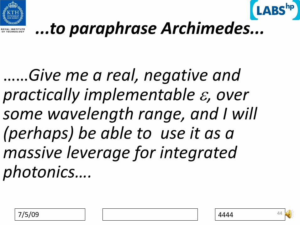
...to paraphrase Archimedes...
44
……Give me a real, negative and practically implementable e, over some wavelength range, and I will (perhaps) be able to use it as a massive leverage for integrated photonics….

7/5/09