Embed Size (px)
Citation preview

Nanoparticle-Based NanophotonicsNanoparticle-Based Nanophotonics
Tadashi Kawazoe : University of TokyoTadashi Kawazoe : University of Tokyo
Particles 2007:Particle-Based Device Technologies
+ E=1/4πk(q/r2)
+ -
Coulomb forceF=Eq=1/4πk(q2/r2)
Electric Field & Interaction by Charges
•These equations are exact for every distances, when we do not consider their wave function. Because this equation is the definition of charge.
I(ωmn)
m
n
Wmn=4π2I/ℏc・pmn2
Propagating light
Electric Field & Interaction by Dipoles
transition
Optical Near-Field
Electric Field
pmn: (transition) electric dipole•We obtained pmn as a physically material parameter by using this relation from the experimental results.
21 2 1 2
5
( ) 3( )( )rU
r
⋅ − ⋅ ⋅= p p p r p r
•The dipole-dipole interaction is correct in nano-region?When the separation of dipoles are broad, it is exact. Because one acts as light emitter and another acts as absorber. However, when it is narrow, the dipoles change and the dipole-dipole interaction also changes. Thus the equation of dipole-dipole interaction should change in nanometric region.
•We call the electromagnetic wave in this region “Optical Near Field” and Its interaction is called “Optical Near Field Interaction”.
Separation<Size of Dipole
Particles 2007:Particle-Based Device Technologies
Nanophotonic deviceMotivation and problems
Nanophotonic deviceMotivation and problems
•I have studied communication networks. However, I have a problem of communication in English. Excuse me, please・・・・・.
Particles 2007:Particle-Based Device Technologies
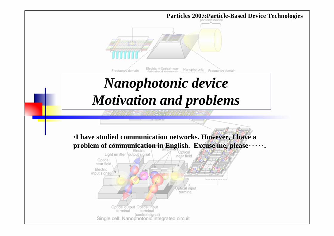
Technology roadmap of optical devicesTechnology roadmap of optical devices
※MIT Microphotonics Center:Communications Technology Roadmap 2005
Particles 2007:Particle-Based Device Technologies

Connections between nanometric deviceConnections between nanometric device
Size of Photonic Devicemm nm
Wavelength of Light
Optical Source
Conventional photonic device Photonic Crystals Plasmonics
Plasmon Condenser
Device
Optical Source
Detector
Fiber
Every device can be isolated.Every device can work
individually
Using Wave Property
Downsize
Nano Optical Source
Both Changes. Optical Source
orOptical Absorber.
μm
Our Target
•Field pattern is changedbut still working for each.
Near-field Coupling
•The device operation is influenced by the load.Load
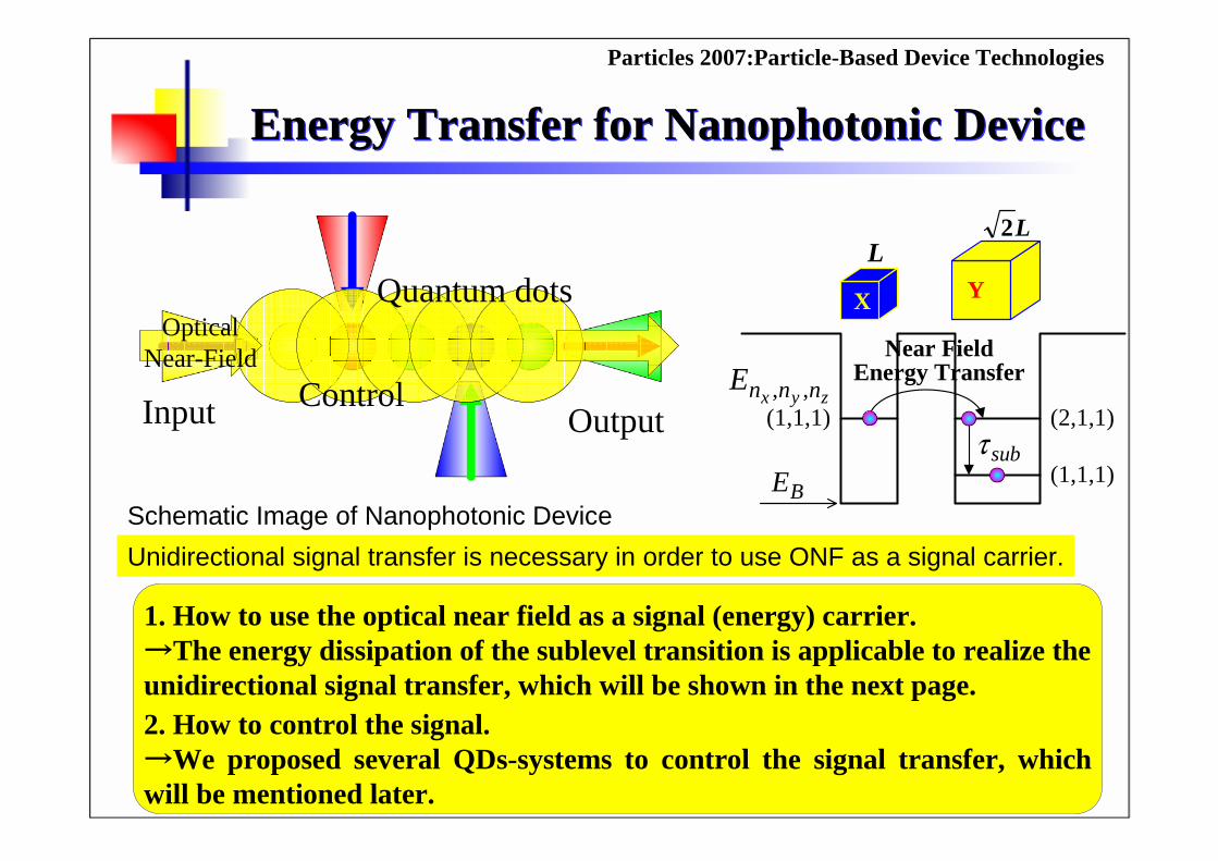
Energy Transfer for Nanophotonic DeviceEnergy Transfer for Nanophotonic Device
Input ControlOutput
1. How to use the optical near field as a signal (energy) carrier.→The energy dissipation of the sublevel transition is applicable to realize the unidirectional signal transfer, which will be shown in the next page.2. How to control the signal. →We proposed several QDs-systems to control the signal transfer, which will be mentioned later.
(1,1,1)
(1,1,1)
(2,1,1)
Near FieldEnergy Transfer
zyx nnnE ,,
BE
LL2
subτ
X YQuantum dotsOptical
Near-Field
Schematic Image of Nanophotonic DeviceTo overcome the diffraction limit, we use the optical near field.Unidirectional signal transfer is necessary in order to use ONF as a signal carrier.
Particles 2007:Particle-Based Device Technologies
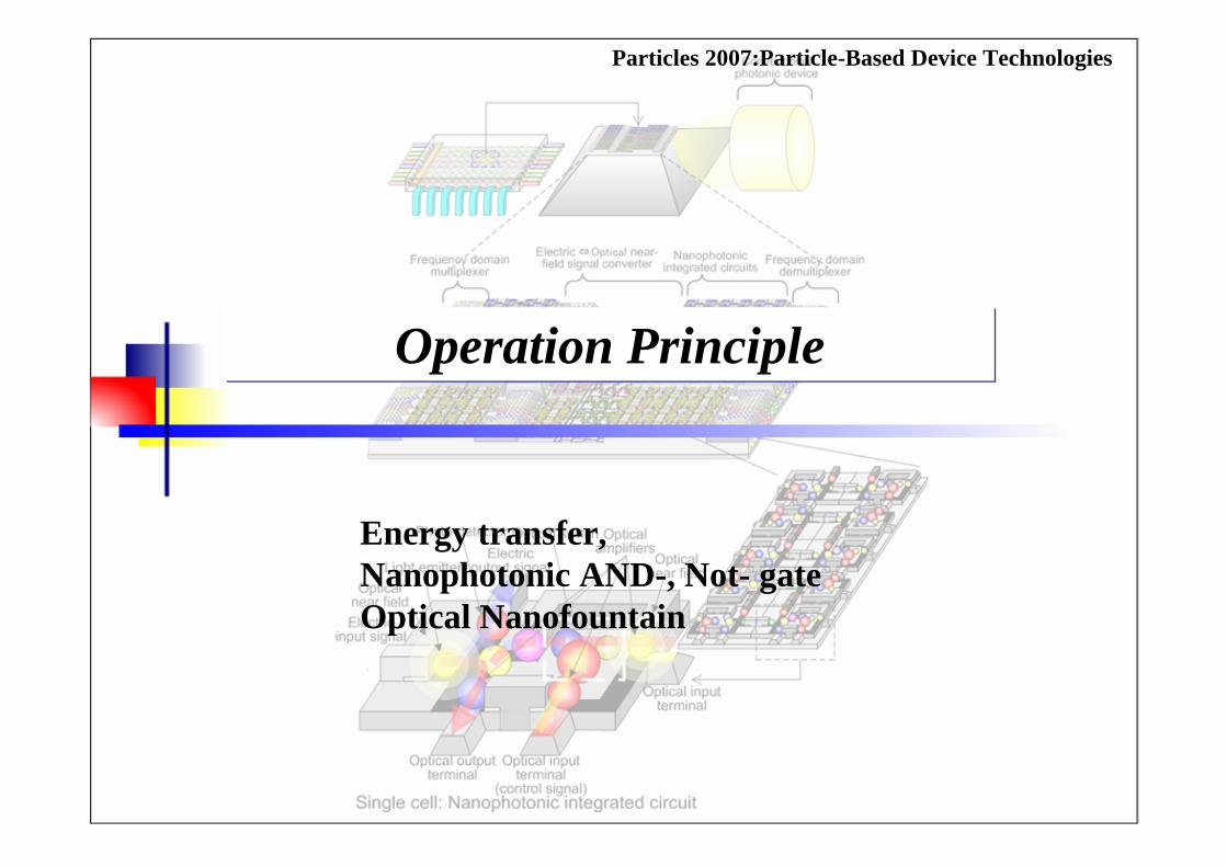
Operation PrincipleOperation Principle
Energy transfer, Nanophotonic AND-, Not- gate Optical Nanofountain
Particles 2007:Particle-Based Device Technologies
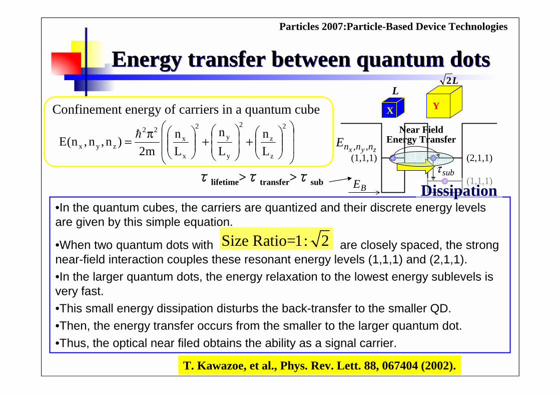
Energy transfer between quantum dotsEnergy transfer between quantum dots
⎟⎟
⎠
⎞
⎜⎜
⎝
⎛⎟⎟⎠
⎞⎜⎜⎝
⎛+⎟
⎟⎠
⎞⎜⎜⎝
⎛+⎟⎟
⎠
⎞⎜⎜⎝
⎛π=2
z
z
2
y
y
2
x
x22
zyx L
n
L
n
L
n
m2)n,n,n(E
Confinement energy of carriers in a quantum cube
(1,1,1)
(1,1,1)
(2,1,1)
Near FieldEnergy Transfer
zyx nnnE ,,
BE
LL2
subτ
X Y
T. Kawazoe, et al., Phys. Rev. Lett. 88, 067404 (2002).
τlifetime>τtransfer>τsub
•In the quantum cubes, the carriers are quantized and their discrete energy levels are given by this simple equation.
•When two quantum dots with are closely spaced, the strong near-field interaction couples these resonant energy levels (1,1,1) and (2,1,1).
•In the larger quantum dots, the energy relaxation to the lowest energy sublevels is very fast.
•This small energy dissipation disturbs the back-transfer to the smaller QD.
•Then, the energy transfer occurs from the smaller to the larger quantum dot.
•Thus, the optical near filed obtains the ability as a signal carrier.
Size Ratio=1: 2
Dissipation
Particles 2007:Particle-Based Device Technologies
OFF StateOFF State
Input Signal
Sweep Out
Output SignalOutput Signal
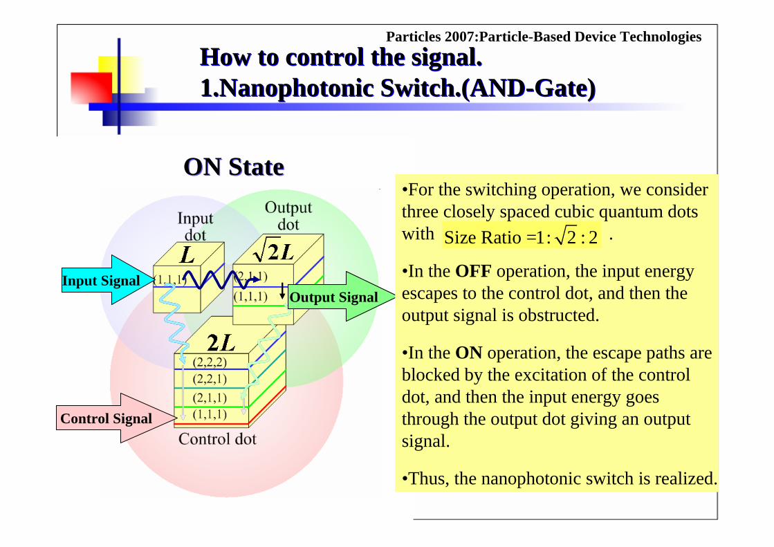
How to control the signal.1.Nanophotonic Switch.(AND-Gate)How to control the signal.1.Nanophotonic Switch.(AND-Gate)
ON StateON State
Input Signal
Control Signal
Output SignalOutput Signal
•For the switching operation, we consider three closely spaced cubic quantum dots with size ratio of .
•In the OFF operation, the input energy escapes to the control dot, and then the output signal is obstructed.
•In the ON operation, the escape paths are blocked by the excitation of the control dot, and then the input energy goes through the output dot giving an output signal.
•Thus, the nanophotonic switch is realized.
Size Ratio =1: 2 : 2
Particles 2007:Particle-Based Device Technologies
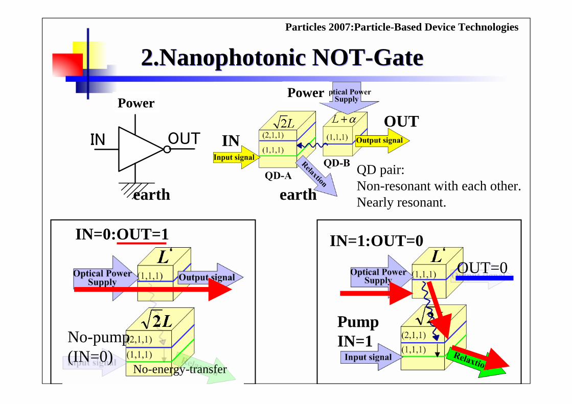
2.Nanophotonic NOT-Gate2.Nanophotonic NOT-Gate
IN=0:OUT=1
PumpIN=1
OUT=0
IN=1:OUT=0
No-pump(IN=0)
No-energy-transfer
+
IN OUT
Power
earth
OUTIN
QD pair:Non-resonant with each other.Nearly resonant.
Power
earth
Particles 2007:Particle-Based Device Technologies
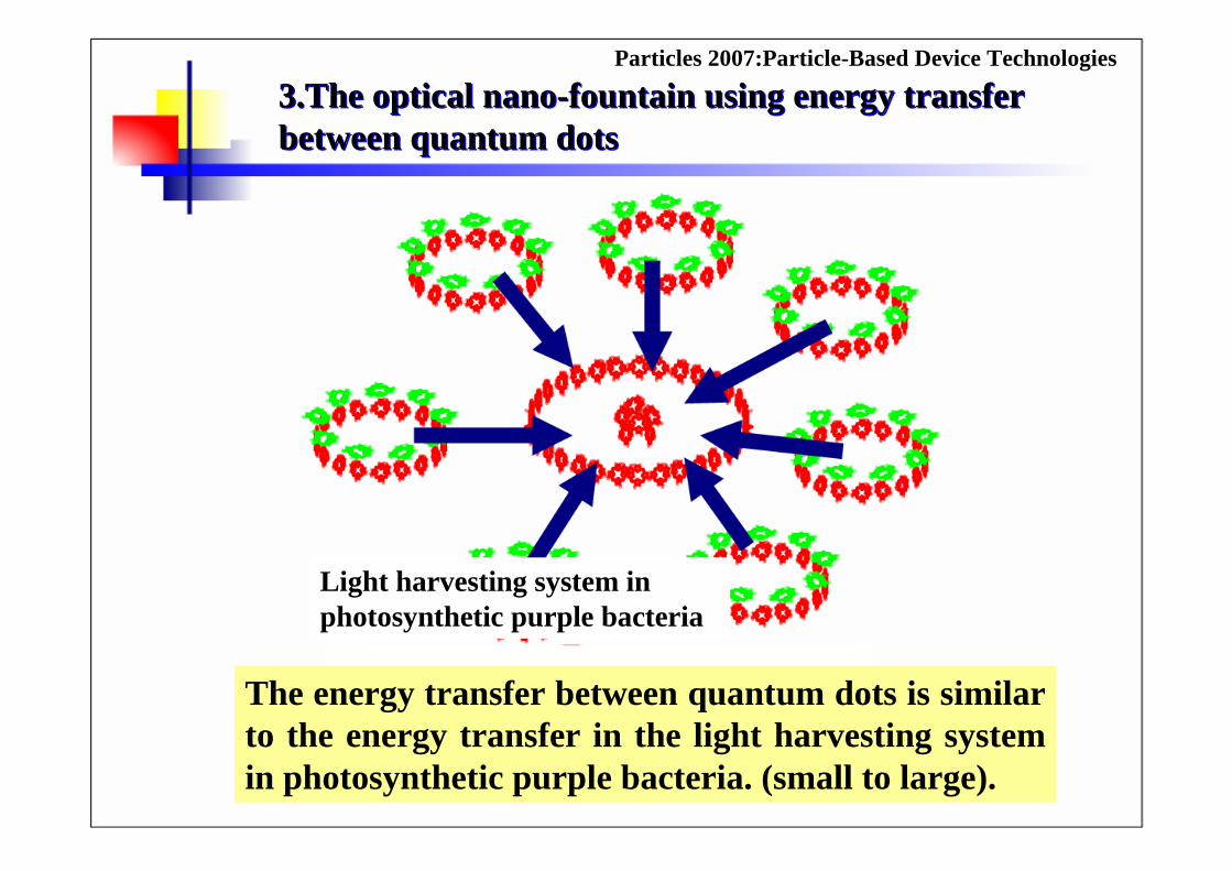
3.The optical nano-fountain using energy transfer between quantum dots3.The optical nano-fountain using energy transfer between quantum dots
Energy dissipation
QD
Light harvesting system in photosynthetic purple bacteria
Particles 2007:Particle-Based Device Technologies
The energy transfer between quantum dots is similar to the energy transfer in the light harvesting system in photosynthetic purple bacteria. (small to large).

Experimental ResultsExperimental Results
Particles 2007:Particle-Based Device Technologies
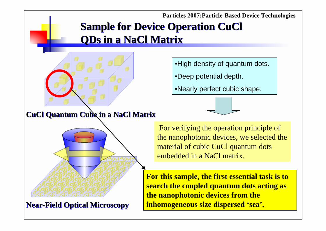
CuCl Quantum Cube in a NaCl MatrixCuCl Quantum Cube in a NaCl Matrix
Near-Field Optical MicroscopyNear-Field Optical Microscopy
Sample for Device Operation CuCl QDs in a NaCl MatrixSample for Device Operation CuCl QDs in a NaCl Matrix
For verifying the operation principle of the nanophotonic devices, we selected the material of cubic CuCl quantum dots embedded in a NaCl matrix.
•High density of quantum dots.
•Deep potential depth.
•Nearly perfect cubic shape.
For this sample, the first essential task is to search the coupled quantum dots acting as the nanophotonic devices from the inhomogeneous size dispersed ‘sea’.
Particles 2007:Particle-Based Device Technologies

JASCO Co. LTD. :SNOM
500nm
Optical Near-Field MicroscopeOptical Near-Field Microscope
Particles 2007:Particle-Based Device Technologies

Experimental results: 1. Nanophotonic SwitchExperimental results: 1. Nanophotonic Switch
OFF StateOFF State
Input Signal
Sweep Out
Output SignalOutput Signal
ON StateON State
Input Signal
Control Signal
Output SignalOutput Signal
Particles 2007:Particle-Based Device Technologies
T.Kawazoe et al., Appl. Phys. Lett. 82, 2957(2003).
0 5 10 15 20 25 30
150
200
INTEN
SIT
Y (
a.u.
)
Time (ns)
Signal Level without pump
pump pump pump
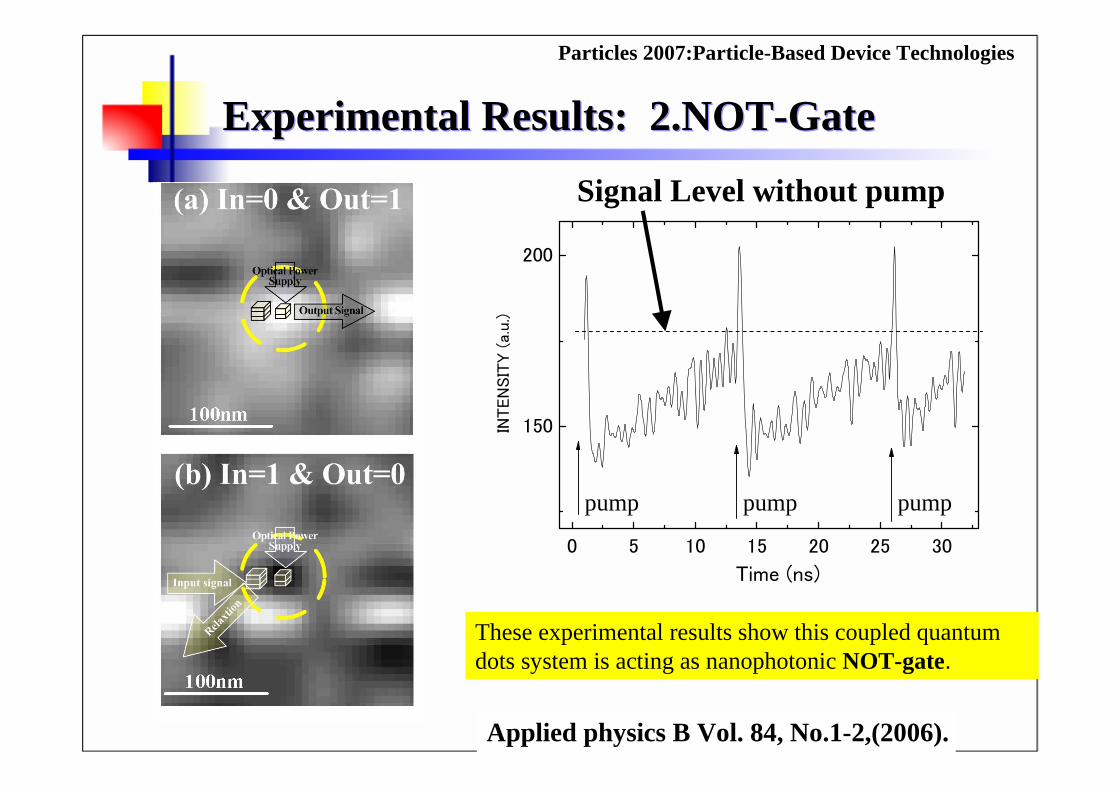
Experimental Results: 2.NOT-Gate Experimental Results: 2.NOT-Gate
These experimental results show this coupled quantum dots system is acting as nanophotonic NOT-gate.
Applied physics B Vol. 84, No.1-2,(2006).
Particles 2007:Particle-Based Device Technologies
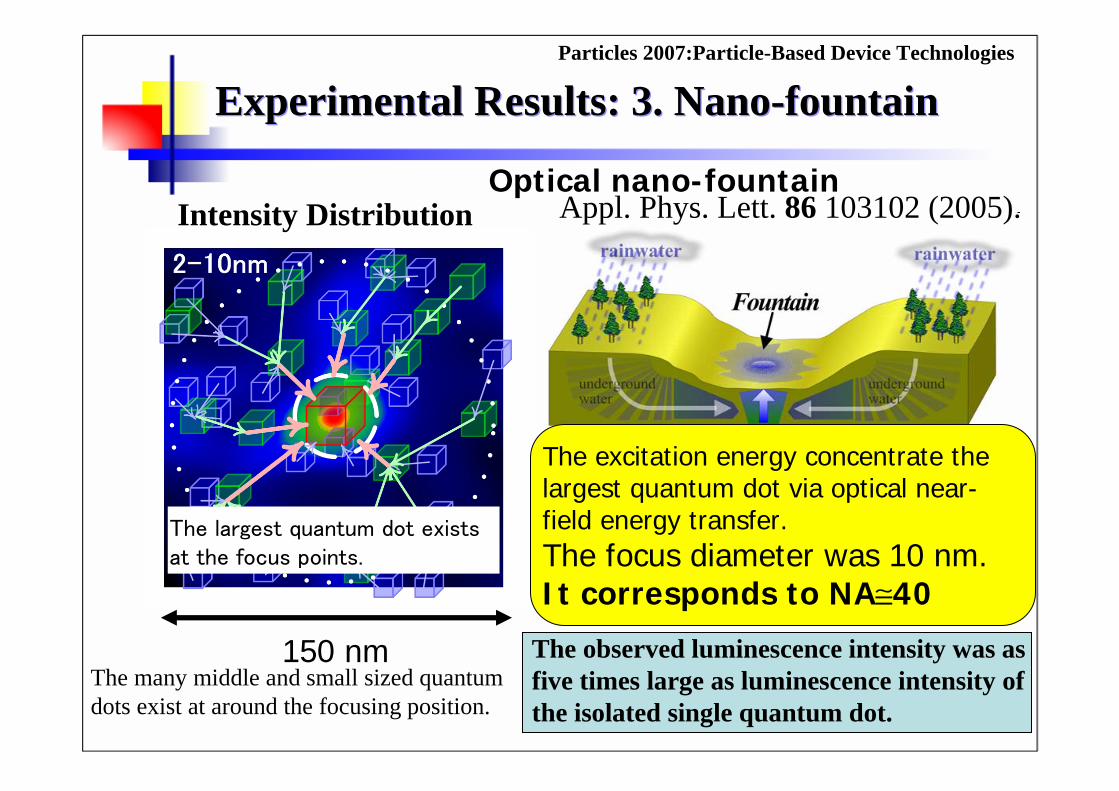
Experimental Results: 3. Nano-fountainExperimental Results: 3. Nano-fountain
150 nm
Optical nano-fountainIntensity Distribution
The largest quantum dot exists at the focus points.
The many middle and small sized quantum dots exist at around the focusing position.
Appl. Phys. Lett. 86 103102 (2005).
The excitation energy concentrate the largest quantum dot via optical near-field energy transfer.The focus diameter was 10 nm.It corresponds to NA≅40
The observed luminescence intensity was as five times large as luminescence intensity of the isolated single quantum dot.
Particles 2007:Particle-Based Device Technologies
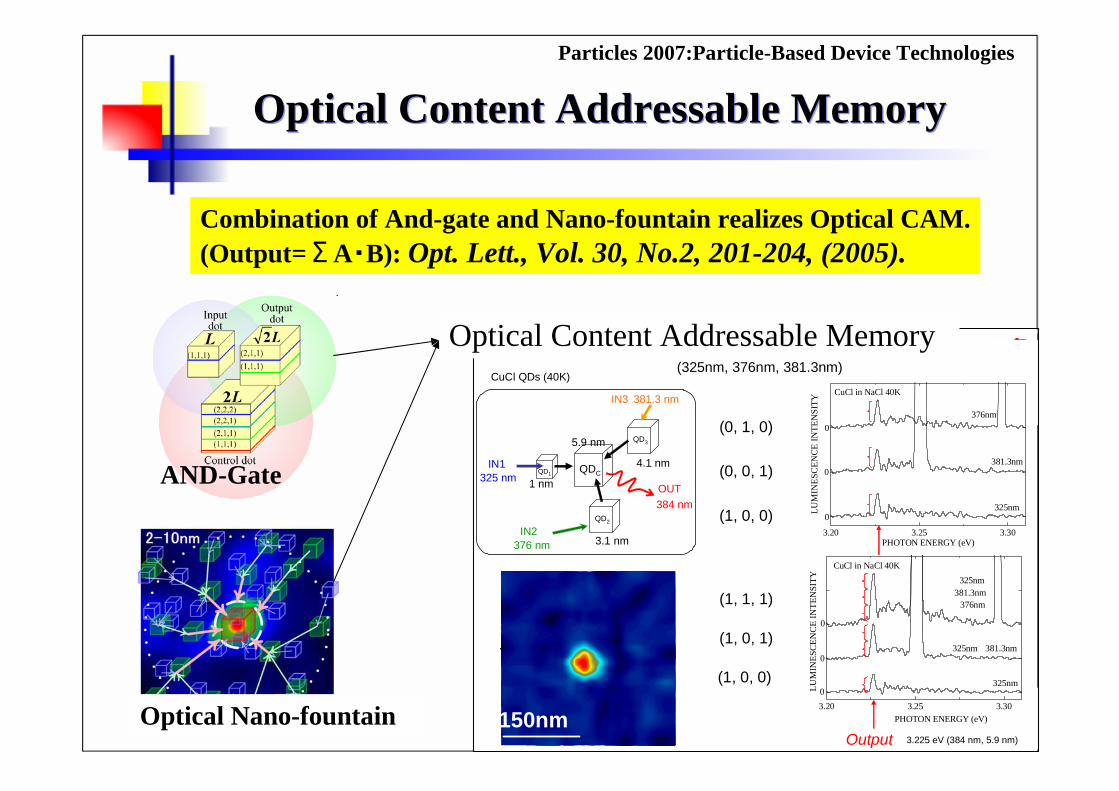
Optical Content Addressable MemoryOptical Content Addressable Memory
Nanophotonics Team 41
3.20 3.25 3.30
CuCl in NaCl 40K
376nm
381.3nm
325nm0
0
LU
MIN
ES
CE
NC
E I
NT
EN
SIT
Y
PHOTON ENERGY (eV)
0
(325nm, 376nm, 381.3nm)
(0, 1, 0)
(0, 0, 1)
(1, 0, 0)
(1, 1, 1)
(1, 0, 1)
(1, 0, 0)
3.20 3.25 3.30
0
0
0
CuCl in NaCl 40K
376nm
381.3nm325nm
325nm
LU
MIN
ESC
EN
CE
IN
TE
NSI
TY
PHOTON ENERGY (eV)
381.3nm325nm
Output
InputSummation 実証実験
3.225 eV (384 nm, 5.9 nm)
150nm
QD2
QD3
QDC
1 nm
3.1 nm
4.1 nm
5.9 nm
QD1325 nmIN1
376 nmIN2
381.3 nmIN3
384 nm
OUT
CuCl QDs (40K)
Optical Content Addressable Memory
AND-Gate
Optical Nano-fountain
Combination of And-gate and Nano-fountain realizes Optical CAM.(Output=ΣA・B): Opt. Lett., Vol. 30, No.2, 201-204, (2005).
Particles 2007:Particle-Based Device Technologies

Broadcasting systemBroadcasting system
Block 1 Block 2 Block m
λ~
~1
μm
~1 μm
IN1: 325 nmIN2: none
0
0.24
200 nm
~1 μm
~1
μm
200 nm
IN1: 325 nmIN2: 384.7 nm
OFF state ON state
IN1325 nm
IN2384.7 nm
Sample: CuCl QD in a NaCl Matrix
Average size: 4.2 nm
Broadcast実証実験
Many AND-Gates
Broadcasting System
Many AND-gates can act as broadcasting system, which delivers the data to many Receivers. :Opt. Express, Vol. 14, 306-313 (2006).
Particles 2007:Particle-Based Device Technologies

Buffering systemBuffering system
375 380 385 390
0
100
200
300
400
500
600
700
WAVELENGTH (nm)
TIM
E D
ELA
Y (
ps)
入力読み出し
0 250 5000
1
2
3
INTEN
SIT
Y (
a.u.)
TIME DELAY (ns)
遅延出力信号
Fitting: t1=1300ps, t2=600ps, Interaction-1=155ps
章動
1往復=1バッファ時間
励起
(入力
)
読み出し
出力移動
エネルギー移動‘
inputOutput
Delayed signal
Buffering system
NOT-Gate
Combination of Nutation and NOT-gate realizes Optical Data buffering system.: CLEO/QELS 2006.
Particles 2007:Particle-Based Device Technologies

Fundamental difference: Conventional and Nanophotonic devices
Conventional photonic device
Determination of operation
•In conventional case, device size may be decreased to diffraction limit.
•However, operating determination is made out side of the device.->device size is large.
•Cascadability has also problem, because there is no determination in inter-device.
•When we connects AND gate and NOT gate, they could not act as NAND gate.
•So for NAND operation, we must design it as another total system as NAND-gate.
no determination
Input Signal
Sweep Out
Output SignalOutput Signal
Nanophotonic device
Dissipations for determination
•In the nanophotonic device, many dissipation parts for determination are in the device.->Total device size is small.
•When we make NAND gate, we only connect AND gate and NOT gate. Because the small dissipation supports each device operation.•This small dissipation also supports low power consumption.
Particles 2007:Particle-Based Device Technologies
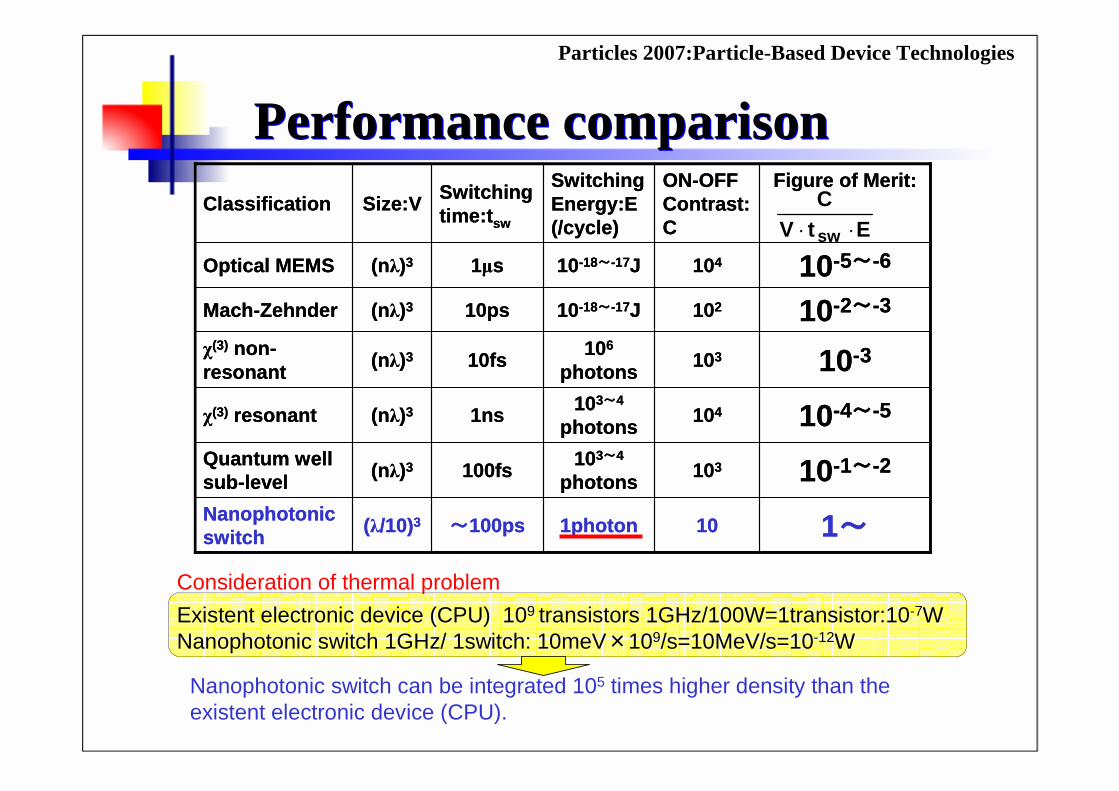
Performance comparisonPerformance comparison
Existent electronic device (CPU) 109 transistors 1GHz/100W=1transistor:10-7WNanophotonic switch 1GHz/ 1switch: 10meV×109/s=10MeV/s=10-12W
Nanophotonic switch can be integrated 105 times higher density than the existent electronic device (CPU).
Consideration of thermal problem
10
103
104
103
102
104
ON-OFF Contrast:C
1~1photon~100ps(λ/10)3Nanophotonicswitch
10-1~-2103~4
photons100fs(nλ)3Quantum well
sub-level
10-4~-5103~4
photons1ns(nλ)3χ(3) resonant
10-3106
photons10fs(nλ)3χ(3) non-
resonant
10-2~-310-18~-17J10ps(nλ)3Mach-Zehnder
10-5~-610-18~-17J1μs(nλ)3Optical MEMS
Figure of Merit:Switching Energy:E (/cycle)
Switching time:tsw
Size:VClassification
10
103
104
103
102
104
ON-OFF Contrast:C
1~1photon~100ps(λ/10)3Nanophotonicswitch
10-1~-2103~4
photons100fs(nλ)3Quantum well
sub-level
10-4~-5103~4
photons1ns(nλ)3χ(3) resonant
10-3106
photons10fs(nλ)3χ(3) non-
resonant
10-2~-310-18~-17J10ps(nλ)3Mach-Zehnder
10-5~-610-18~-17J1μs(nλ)3Optical MEMS
Figure of Merit:Switching Energy:E (/cycle)
Switching time:tsw
Size:VClassificationEtV
C
sw ⋅⋅
Particles 2007:Particle-Based Device Technologies

Experimental Results for other materialsExperimental Results for other materials
Particles 2007:Particle-Based Device Technologies

Other Logic circuitsOther Logic circuits
Logic circuits
Particles 2007:Particle-Based Device Technologies
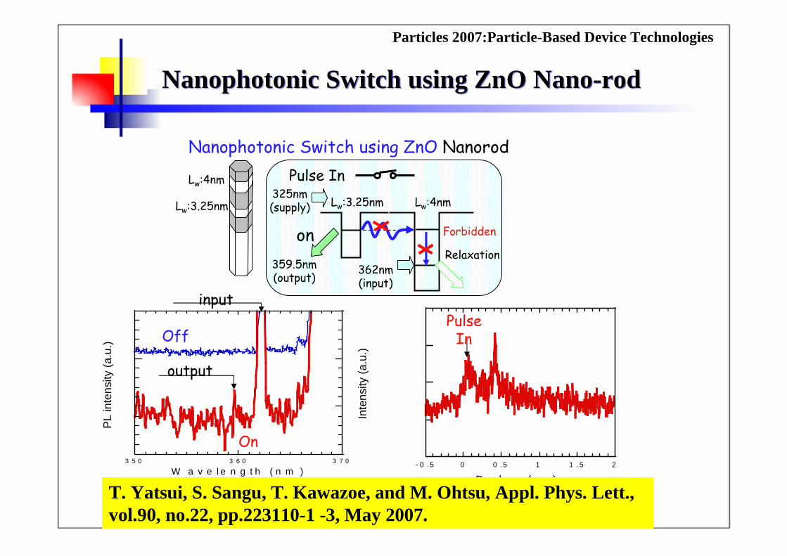
Nanophotonic Switch using ZnO Nanorod
Lw:3.25nm
Lw:4nm
359.5nm(output)
362nm(input)
Pulse In
Relaxation
325nm (supply)
Forbidden
Lw:3.25nm Lw:4nm
on
- 0 . 5 0 0 . 5 1 1 . 5 2
D e l a y ( n s )
PulseIn
3 5 0 3 6 0 3 7 0
W a v e l e n g t h ( n m )
output
On
PL
inte
nsi
ty (
a.u
.)
OffIn
ten
sity
(a
.u.)
input
Nanophotonic Switch using ZnO Nano-rodNanophotonic Switch using ZnO Nano-rod
T. Yatsui, S. Sangu, T. Kawazoe, and M. Ohtsu, Appl. Phys. Lett., vol.90, no.22, pp.223110-1 -3, May 2007.
Particles 2007:Particle-Based Device Technologies
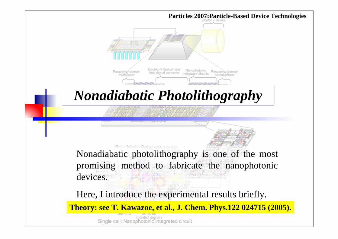
Nonadiabatic PhotolithographyNonadiabatic Photolithography
Nonadiabatic photolithography is one of the most promising method to fabricate the nanophotonic devices.
Here, I introduce the experimental results briefly.Theory: see T. Kawazoe, et al., J. Chem. Phys.122 024715 (2005).
Particles 2007:Particle-Based Device Technologies

Background & Motivation
Too expensive!!
We found the Nonadiabatic Photochemical Reaction.the Nonadiabatic Photochemical Reaction.
And proposed the photolithographyusing the nonadiabatic reaction.(Nonadiabatic photolithography)
Low price of equipmentsHigh resolutionLow power consumption
Cost of equipment is $100milion.Power consumption is 100billion KWh/year in Japan 2005.
•Photolithography is the practical high-throughput method to produce electronic and photonic devices
•In order to make patterns much smaller, the wavelength of a light source must be shorten, due to the diffraction limit
Particles 2007:Particle-Based Device Technologies

Internuclear Distance
Pot
enti
al E
ner
gyAdiabatic reaction
ActivationEnergy
molecule
light
molecule
dissociation
Potential Curves of Electron in Molecular OrbitalPotential Curves of Electron in Molecular Orbital
Particles 2007:Particle-Based Device Technologies

T.Kawazoe、K.Kobayashi、S.Takubo、M.Ohtsu “Nonadiabatic photo-dissociation process using an optical near field“Journal of Chemical Physics 、122、024715(2005)
Far Field: adiabatic Near Field: nonadiabatic
e-
Nuclear
Nonadiabatic photochemical reactionNonadiabatic photochemical reaction
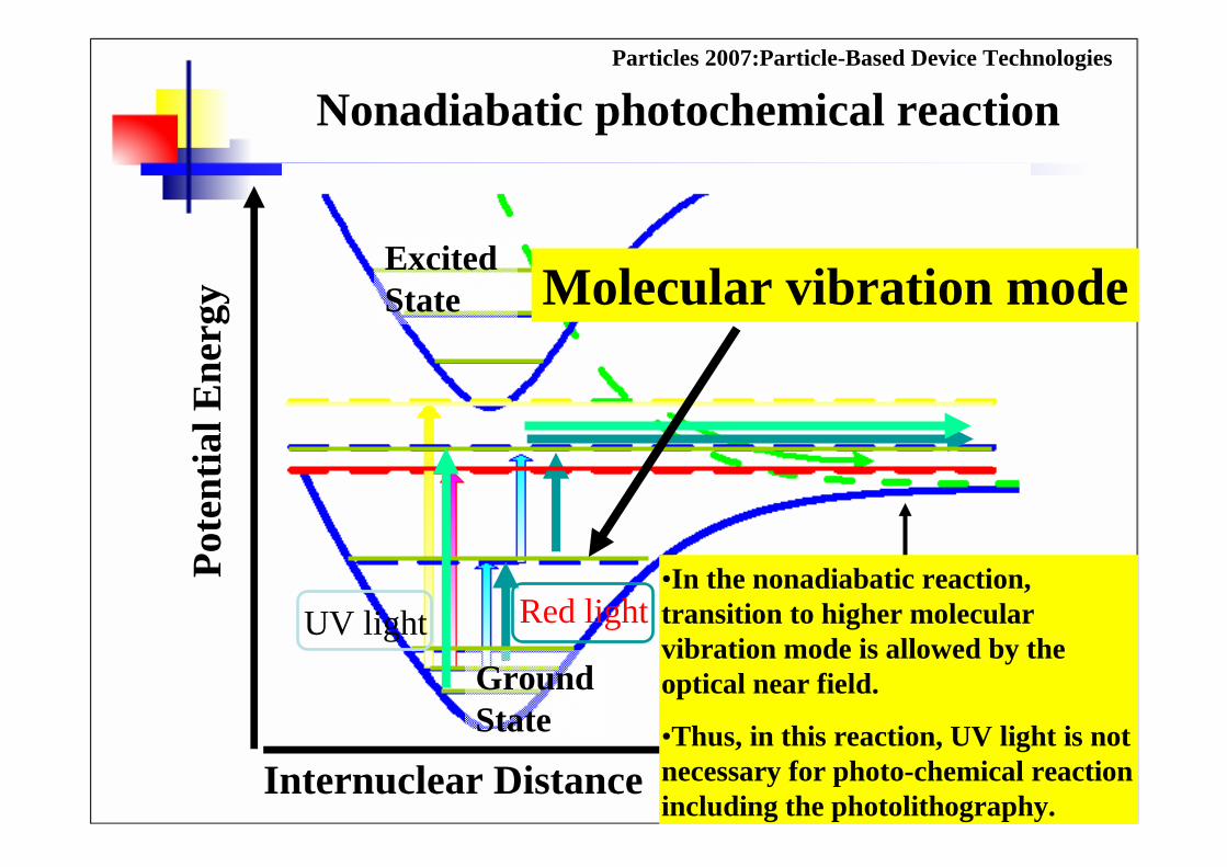
Steeply spatial gradient of optical near field can excite the molecular vibration mode directly.
Particles 2007:Particle-Based Device Technologies
ActivationEnergy
Pot
enti
al E
ner
gy
Internuclear Distance
UV light Red light
Molecular vibration modeExcitedState
GroundState
•In the nonadiabatic reaction, transition to higher molecular vibration mode is allowed by the optical near field.
•Thus, in this reaction, UV light is not necessary for photo-chemical reaction including the photolithography.
Nonadiabatic photochemical reactionParticles 2007:Particle-Based Device Technologies

Contact exposure
Near-field exposure
Nonadiabatic exposure
H. Yonemitsu, T. Kawazoe, et. al, J. Lumin. 122-123, PP.230-233 (2007).
Comparison of typical fabricated resultsComparison of typical fabricated resultsParticles 2007:Particle-Based Device Technologies

This method increase in the resolution of photolithography. By using 550 nm light,
Fabrication of 45nm-L&S was succeeded.
Φ100nm ring-array FWHM 50nm Fabricated Cr-Line
HP125nm: 2-dimentional array HP45nm: L&S
Application Nonadiabatic Reaction to Photolithography II
Particles 2007:Particle-Based Device Technologies

Prototype stepper by Canon Co. LTD. & Univ. TokyoPrototype stepper by Canon Co. LTD. & Univ. Tokyo
32nm L&S
Prototype stepper was completed (2006).It has 32nm resolution, but its cost was less than 10% of EUV stepper and EB lithography.
Particles 2007:Particle-Based Device Technologies