Embed Size (px)
Citation preview

1
State of Art Techniques in Digital to Analog Converter Design
Dr. Rahmi Hezar
Senior Member of Technical Staff Kilby Labs, Texas Instruments

2
What to Expect from a DAC Short answer: Everything
Reality: Depends on the application with different weighting
Audio Applications: a. Linearity is the king: Improves dynamic range, reduces distortion, reduces
requirements on the amplifier, just better listening experience. b. Power Consumption is somewhat critical: On phones and tablets DAC is not
the main source of power consumption c. Out of band noise: Some what Important needs large capacitors to remove
RF Applications: Absolute linearity is relaxed compared to audio but high clock speeds make it
challenging. Power now is the king: RF circuits drain the battery very quickly and heat the
chip, create reliability problems. Out of band noise is more critical compared to audio, requires expensive, very
large, high-Q band-pass filters to meet tight RF masks requirements. Other: DACs are the bottleneck in ADC design. A Sigma Delta ADC is as good as
its feedback DAC

3
What to Expect from this Presentation Short answer: Everything about DACs
Reality: Smart Architectures and Signal Processing Methods for DACs
Analog design side of DACs is very simple and well developed a. Current steering DACs: Summing current sources via switches b. Voltage DACs: Summing voltages via switching capacitors
We want them to be a. Infinitely fast b. Absolutely perfect (no change from the original value, no variation) c. Add no distortion, no noise
Fact: they are imperfect and never fast enough Question: how do we use them so that their weaknesses are not
exposed and strength are shown? Answer: lies in the rest of this presentation

4
Smart Architecture Design:
Cascaded Modulator For Oversampled Digital-to-Analog Converters
4

5
A Brief Look at the Audio DAC’s Past
Modern Day Oversampled DACs
From CD Childhood days 1980s
First Oversampled DACs 1990s
Single bit DAC
Multi-level
DAC Nyquist rate input
Filtering cap
Filtering cap
1-bit output at OSR*Fs

6
Switch-Cap & Current Steering
Pros- Less sensitive to Phase-noise Less sensitive to ISI if settling is fast Allows for a simple single ended voltage output circuit Cons- Sensitive to static element mismatch Very power/area hungry so no of DAC levels is limited Out of band noise is high needs very good filtering Does not scale with the process very sensitive to high frequency noise
Pros- Allows for very small area implementation especially in CMOS processes. Can be clocked at much faster rates Less prone to aliasing due to CT nature Scales very well with the process Overall very low power circuit, total current is about IREF
Cons- Sensitive to static element mismatch More sensitive to jitter if OBN is high Sensitive to ISI

7
Dominant Error Sources in DACs DAC Element Mismatch DAC Asymmetrical Switching (ISI) Clock Jitter & Amplifier Nonlinearity
( )[ ] ( )[ ]
Errors TimeFall Dynamic
1]1[][,
Errors TimeRise Dynamic
]1[][1
,
ErrorsMismatch Element Static
1][][ 11 ∑∑∑
=−−
==
⋅−+−⋅−=N
ininiifnini
N
iir
N
iniin SSSSSDACe δδε

8
Impact of DAC Non-linearity
We need to reduce out of band noise
Push in- band down

9
Single-Bit and Multi-bit Trade-off
Suppress in-band & out of band noise
Single Bit DAC: More out of band noise Faster clocking to get the in-band low Element mismatch does not matter
BUT, worst case scenario for ISI, there is no way to correct for it
Multi Bit DAC: Reduce both Out of Band Noise and Inband Slower clock rates relax the ISI errors Multi-level glitch errors have less impact BUT, worst case scenario for mismatch Good news: There are algorithms to shape element mismatch

10
Cost of Filtering OBN
Classical RC Filtering of out of band noise
Area usage is dominated by RC filtering

11
Try Analog-FIR Filtering
Unity FIR does not provide enough suppression.
8-tap
16-tap
AFIR DAC
12
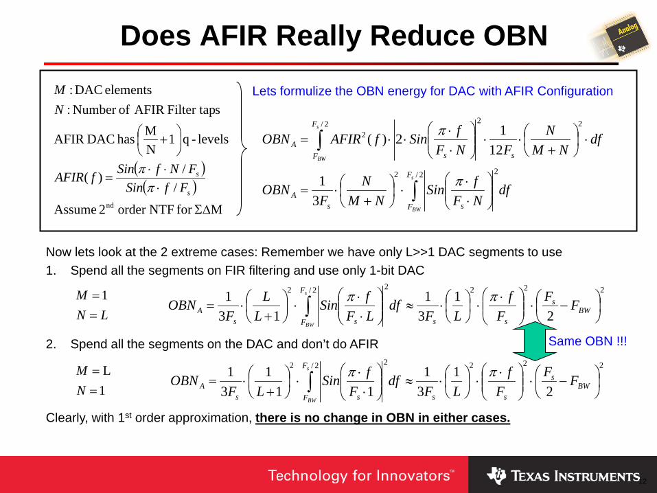
Does AFIR Really Reduce OBN
dfNFfSin
NMN
FOBN
dfNM
NFNF
fSinfAFIROBN
s
BW
s
BW
F
F ssA
F
F ssA
∫
∫
⋅⋅
⋅
+⋅=
⋅
+⋅⋅
⋅⋅
⋅⋅=
2/ 22
22/ 2
2
31
1212)(
π
π
( )( )
Mfor NTForder 2 Assume
//)(
levels-q 1NM has DAC AFIR
sFilter tap AFIR ofNumber :elements DAC :
nd Σ∆
⋅⋅⋅
=
+
s
s
FfSinFNfSinfAFIR
NM
ππ
Lets formulize the OBN energy for DAC with AFIR Configuration
Now lets look at the 2 extreme cases: Remember we have only L>>1 DAC segments to use 1. Spend all the segments on FIR filtering and use only 1-bit DAC
2. Spend all the segments on the DAC and don’t do AFIR
Clearly, with 1st order approximation, there is no change in OBN in either cases.
LNM==1 2222/ 22
21
31
131
−⋅
⋅⋅
⋅≈
⋅⋅
⋅
+⋅= ∫ BW
s
ss
F
F ssA FF
Ff
LFdf
LFfSin
LL
FOBN
s
BW
ππ
2222/ 22
21
31
111
31
−⋅
⋅⋅
⋅≈
⋅⋅
⋅
+⋅= ∫ BW
s
ss
F
F ssA FF
Ff
LFdf
FfSin
LFOBN
s
BW
ππ1L
==
NM
Same OBN !!!

13
Try Adding More Quantizer Levels
Similar type of reduction to AFIR plus the digital complexity
Increase quantizer resolution in the modulator
High Res. DAC
25-Level DAC Element Matching is more difficult
14
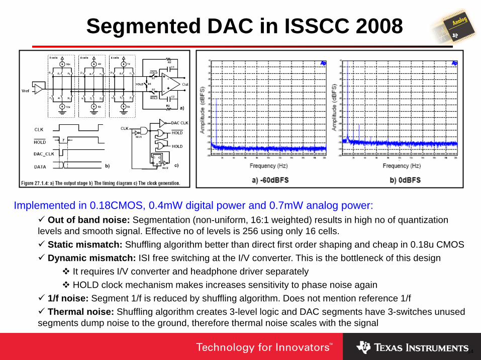
Segmented DAC in ISSCC 2008
Implemented in 0.18CMOS, 0.4mW digital power and 0.7mW analog power: Out of band noise: Segmentation (non-uniform, 16:1 weighted) results in high no of quantization levels and smooth signal. Effective no of levels is 256 using only 16 cells. Static mismatch: Shuffling algorithm better than direct first order shaping and cheap in 0.18u CMOS Dynamic mismatch: ISI free switching at the I/V converter. This is the bottleneck of this design
It requires I/V converter and headphone driver separately HOLD clock mechanism makes increases sensitivity to phase noise again
1/f noise: Segment 1/f is reduced by shuffling algorithm. Does not mention reference 1/f Thermal noise: Shuffling algorithm creates 3-level logic and DAC segments have 3-switches unused segments dump noise to the ground, therefore thermal noise scales with the signal

15
Cascaded Modulator Architecture Presented in ISSCC 2010
( ) ( ) ( ) ( )zEzNTFK
zXzY 21
⋅⋅+=
For a 2-level cascade
Resolution is boosted by K.
For N-level cascades
( ) ( ) ( ) ( )zEzNTFK
zXzY NN ⋅⋅+= −1
1

16
Impact of Mismatch on Resolution
( ) ( ) ( ) ( )zEzNTFK
zXzY 21
⋅⋅+=
( ) ( ) ( ) ( ) ( ) ( )zEzNTFK
zEzNTFKK
zXzYaa
d21
11 ⋅⋅+⋅⋅
−+=
Ideal output for a 2-level cascade
If digital Kd and analog Ka do not match
Mismatch between Kd and Ka is shaped inherently Mismatches between the DACs are shaped
similarly

17
This is not MASH
• Purpose of MASH is to get higher order from simple 2nd and 1st order modulators. – Same can be achieved with higher order single loop – The purpose of Cascade is to get finer quantization
from coarse quantized modulators.
• MASH sub-modulators are summed in digital domain always – Cascaded modulators are summed in analog
domain.
• MASH is very sensitive to analog/digital mismatch – Cascaded architecture has built in shaping

18
Reducing OBN Cost Effectively
Thermal noise floor
Primary Modulator Only 2-level Cascading 3-level Cascading 4-level Cascading
Impact on OBN is huge: By cascading smaller and smaller DACs, out of band noise can be pushed down to the thermal floor.

19
Impact of Cascading on Area
Cascaded architecture with secondary DAC
Resolution is increased significantly with a small DAC

20
Comparing to Segmented DACs
Segmentation and Cascading are not exclusive
Segmentation is used for high resolution modulators

21
What is Pulse Width Modulation? PWM: Convert amplitude quantized signals to time representation by changing the pulse width of a carrier signal.
What is driving this? I. DACs and ADCs are now all integrated with the massive digital cores in CMOS II. Shrinking CMOS technology is leaving no head room to implement reliable
multi level amplitude quantization III. However, CMOS speeds are always going up IV. So Time Quantization is getting cheaper and Amp Quantization is getting
expensive Adapt or die

22
Using PWM and AFIR in DAC
PWM: M-level data @ Fs 2-level data @ 2*M*Fs – 1-bit data is inherently insensitive to mismatch – Reduced sensitivity to asymmetrical switching

23
Why Not stay at PCM and use DWA?
Noise shaping loop
Mismatch shaping loop Note: If MTF=z-1 then it can simply be implemented as barrel shifter (1st order shaping)
Source of the tone: Noise shaping SDM has idle tones, activity created by “Mismatch shaping loop” amplifies these idle tones. Solution: Tonal free SDM design with dither or chaos.
Source of the tone: Mismatch shaper has idle tones, this loop combined with ISI introduces FM modulated tones specially at small signal swings. Solution: Dithering in SDM does not help, dithering here reduces the effect if static mismatch shaping. We can add DC tone and move the tones outside the audio band.
1st order mismatch shaping No dither anywhere
2nd order mismatch shaping No dither anywhere
Tones can be pushed out by adding DC

24
AFIR and PWM Spectrum
AFIR notch locations align with PWM harmonics
AFIR
PWM spectrum

25
AFIR DAC Circuit

26
Effect of Mismatch on AFIR Ideal AFIR DAC
1% mismatch
5% mismatch 10% mismatch
27
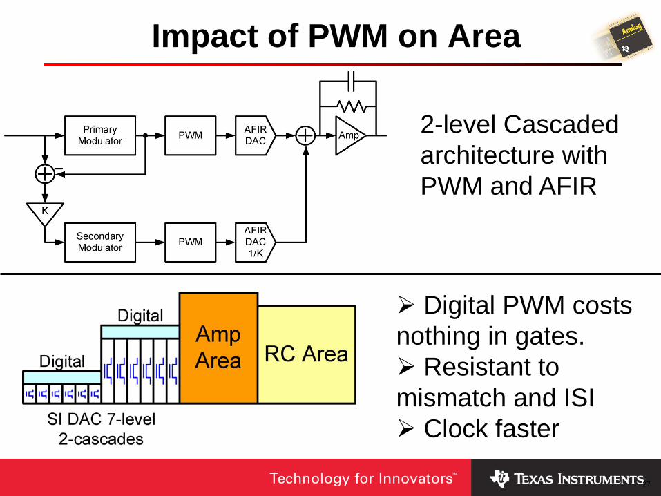
Impact of PWM on Area
2-level Cascaded architecture with PWM and AFIR
Digital PWM costs nothing in gates. Resistant to mismatch and ISI Clock faster
28
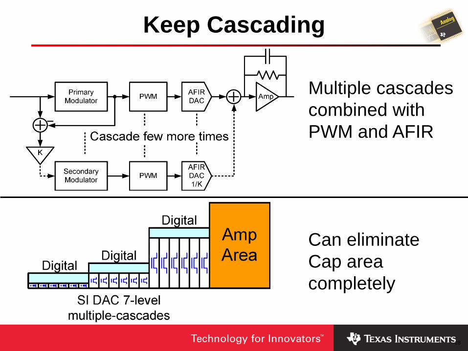
Keep Cascading
Multiple cascades combined with PWM and AFIR
Can eliminate Cap area completely

29
Measurement Results
Very low distortion at -3dB signal 2nd harmonic is down by 120dB 3rd harmonic is down by 118dB 60 Hz is visible around signal and DC
-3dB signal

30
Measurement Results
No spurs and idle tones visible at low signal swing either
60 Hz and its harmonics is still visible around DC
-60dB signal

31
Performance Summary Process 45nm CMOS
Supplies 1.4V Analog/1.1V Digital
Full-scale differential output 176uA peak to peak
Digital power/DAC 0.1mW
Analog power/DAC 0.4mW
Total DAC area 0.045mm2
OSR 64
Clock Frequency 3.072MHz modulator clock
202.752MHz DAC clock Dynamic Range (A-weighted) 110dB
THD+N -100dB

32
Summary
Cascaded Modulator Architecture reduced out of band noise efficiently
Reduced sensitivity to analog error sources
Reduced RC area cost for post filtering
Analog amplifier design requirements are relaxed too.
Smaller dV/dt transitions allow a slower amplifier with low area and power.

33
Where does it stand?
ADI
ADI STNXP
Wolfson
Cirrus
Cirrus
Maxim
National
TI-3254
TI-3254
TI-3106
TI
TI-Phoenix
TARGET ZONE
STNXP
Black True ground Blue VCM driver Red External caps
I don’t see a clear indication that ADI is using the 3-level DAC (108dB DR) published in ISSCC08
ST-NXP is very focused on wireless requirements such as working with 32kHz RTC clock (in fact only one claiming this), true ground swing, implemented in a CMOS process, and ~100dB DR
Unfortunately process information for most of these are not available.
TI-TWL6040 (Phoenix) numbers are from the spec document and not silicon data
There is sort of a barrier line indicated in green on the graph above for performance and power trade-off when looking at existing designs.
Our proposed architecture today can deliver best in the market performance and will be in a class of its own.
Cascading

34
Smart Signal Processing How to Linearize a DAC?
It is all in how you use it
•34

35
ISI-errors and modeling • Errors depend on the
previous symbol
• Can be modelled ISIn=f(sn,sn-1)
• f() can be linear for symmetrical switching – Shaped by the mismatch
shaper (correlated)
• Non-linear part: – Can be assigned to rising
edge only – Un-correlated error
Segmentwaveform
ISI-errorwaveform
sn sn+1 sn+2
sn
ISIn

36
The popular DWA a perfect tone generator
• Simple & popular scheme – Barrel shifter
• A.k.a ”segment rotation”
• Variable rotation speed: – Proportional to the
signal xn – ”VCO” operation – Frequency Modulated
idle tones
pn
0
M-2
M-1
4
1
2
3Turn-onxn seg-ments
M-segments
Circular pointer:pn+1=modM(pn+xn)

37
Generic mis-match shaper
•DWA: H(z)=1/(z-1) •1st order ΣΔ
H(z)
H(z)
H(z)
Q
x[n]From Noise Shaper
Segment 1Segment 2
Segment N DAC
x[n] out of N segments on
VectorQuantizer

38
Max. Rate pattern: Midscale
+F.S.0-F.S.
1/2
Transitiondensity
Tone at fclk/2

39
Pattern for ±1/3 Full Scale
+F.S.0-F.S.
1/2
Transitiondensity
1/3
-1/3 1/3
Tone at fclk/3

40
Pattern for ±1/2 Full Scale
+F.S.0-F.S.
1/2
Transitiondensity
-1/2 1/2
1/4
Tone at fclk/4

41
Pattern for ±1/5 Full Scale
+F.S.0-F.S.
1/2
TransitionDensity/rate
-1/5
2/5
Tone at fclk/5
1/5

42
DWA: Max. Theoretical rate
+F.S.0-F.S.
1/2
TransitionDensity/rate
Theoretical Max.Nonlinear: 1-|x|Even harmonics
+100%
corre
lation
Never
-100% correlation
Never

43
FM idle tones : low level THD issue
0 32k2k 4k 6k 8k 10k 12k 14k 16k 18k 20k 22k 24k 26k 28k 30k19.532k1.984k
Hz
-140
-60
-135
-130
-125
-120
-115
-110
-105
-100
-95
-90
-85
-80
-75
-70
-65
-111.798
-131.178
dBr A
•-60dB sine, •No DC: •FM of idle tone gives harmonics
•-60dB sine+0.4% DC:
•FM of 19.5kHz idle tone ”carrier”
•3rd harm.
•”carrier”

44
DWA+ISI Simulation examples
•T_rise=10ps •A_DC=0V
•T_rise=20ps •A_DC=0V
•T_rise=10ps •A_DC=1mV
•T_rise=10ps •A_DC=10mV
•20ps/Ts=0.006%

45
DWA+ISI: a bad cocktail.. • Large signal:
– V-shape transition rate / mean ISI error vs. signal xn – Abs(xn) type non-linearity - Even-order harmonics – Constant THD ratio vs. level
• Small-signal: – Signal xn jitters across the midscale point due to the
Noise shaper activity – De-correlation of the ISI-error: no high-pass shaping – FM tone frequency proportional to xn: (100% mod ->
fclk) – THD due to FM tones – both even and odd order
• nm-scale design: – Increased clock does not help: ISI goes up and error
is concentrated in tones (not spread spectrum)

46
Prior-art solutions to ISI • ”DC Dither” to shift tones out of band
– Popular but just moves the problem
• Return-to-zero (RTZ) – Increased current, sensitive to timing accuracy/jitter
• Sample and hold de-glitching – Used to de-glitch R2R DACs in early CD players
• Mismatch shaping with reduced transition rate[4] – Reduce ISI at the cost of mismatch shaping
• Pulse Width Modulation (ISSCC’2010) – Great but requires high frequency clock
• Re-spins and layout tweaking of the analog...

47
ISI-Shaper target
Audio band
+F.S.0-F.S.
1/2
TransitionDensity/rate
ISI-Shaping target
LinearNo in-band tones
Max. Max.
Linear range

48
The novel ISI shaping algorithm
HMLF(z)
xnFrom the modulator
M
MismatchShaping
Loop
ditherM
z-1
HILF(z)
VQ
M-segment
Unit Element
DAC
0.5
M
M
M
Rtran
ISIShaping
Loop
M
DAC Output
Sign
M
ISI
S
Sn-1 Sn ISIn0 0 00 1 11 0 01 1 0M
M

49
Single segment spectra
103
104
105
106
-90
-80
-70
-60
-50
-40
-30
-20
-10
0
frequency - Hz
Spe
ctra
l den
sity
- dB
103
104
105
106
-90
-80
-70
-60
-50
-40
-30
-20
-10
0ISI error
frequency - Hz
Spe
ctra
l den
sity
- dB
•1st/1st order ISI-shaper, Rtran=0.25
•ISI-error •Segment (static mismatch error)

50
45nm Audio DAC implementation
Inte
rpol
atio
n Primary ISI-Shaper
Secondary ISI-Shaper
CS-DAC
CS-DAC
Rf
Rf
+
-Vout
-0.71V
0.71V
H(z)
K
Primary Modulator
Secondary Modulator
fCLK=3.072MHz
2-stage Cascaded ModulatorArchitecture
33-L Quant
H(z)
NRZ DACs
33-L Quant
CascadedModulator
1/K scaling

51
Output at -6dB using DWA

52
Output at -6dB using ISI Shaper
•CS-DAC Direct Output •Using ext. I2V

53
Output at -60dB using DWA

54
Output at -60 dB using ISI Shaper

55
45nm DAC: Amplitude sweep
•Near constant THD ratio •Using DWA as expected •Due to ISI errors

56
45nm DAC summary

57
Conclusions
• DWA+ISI gives high amplitude THD and low level tones/noise problems – Concentrates ISI energy in in-band tones
• ISI is hard to fight using analog techniques – Goes against the desire for fast cycle design of SoCs – Goes against the desire to clock fast in nm scale CMOS
• The novel ISI shaper: – Excellent audio performance – even in 45nm – helps fast cycle SoC design – Digitally assisted analog solution to fight ISI – Provides robustness to analog imperfection