Embed Size (px)
Citation preview

Southern Illinois University CarbondaleOpenSIUC
Dissertations Theses and Dissertations
12-1-2014
LOW-POWER LOW-VOLTAGE ANALOGCIRCUIT TECHNIQUES FOR WIRELESSSENSORSChenglong ZhangSouthern Illinois University Carbondale, [email protected]
Follow this and additional works at: http://opensiuc.lib.siu.edu/dissertations
This Open Access Dissertation is brought to you for free and open access by the Theses and Dissertations at OpenSIUC. It has been accepted forinclusion in Dissertations by an authorized administrator of OpenSIUC. For more information, please contact [email protected].
Recommended CitationZhang, Chenglong, "LOW-POWER LOW-VOLTAGE ANALOG CIRCUIT TECHNIQUES FOR WIRELESS SENSORS" (2014).Dissertations. Paper 982.

LOW-POWER LOW-VOLTAGE ANALOG CIRCUIT TECHNIQUES FOR WIRELESS SENSORS
by
Chenglong Zhang
B.S., Huazhong University of Sci. & Tech., 2005
M.S., Huazhong University of Sci. & Tech., 2007
A Dissertation
Submitted in Partial Fulfillment of the Requirements for the
Doctor of Philosophy Degree
Department of Electrical and Computer Engineering
in the Graduate School
Southern Illinois University Carbondale
December, 2014

DISSERTATION APPROVAL
LOW-POWER LOW-VOLTAGE ANALOG CIRCUIT TECHNIQUES FOR WIRELESS SENSORS
By
Chenglong Zhang
A Dissertation Submitted in Partial
Fulfillment of the Requirements
for the Degree of
Doctor of Philosophy
in the field of Electrical and Computer Engineering
Approved by:
Dr. Wang Haibo
Dr. Ahmed Shaikh
Dr. Themistoklis Haniotakis
Dr. Qin Jun
Dr. Zhu Michelle
Graduate School
Southern Illinois University Carbondale
November 4th, 2014

i
AN ABSTRACT OF THE DISSERTATION
CHENGLONG ZHANG, for the Doctor of Philosophy degree in ELECTRICAL &
COMPUTER ENGINEERING, presented on Nov. 4th, 2014, at Southern Illinois
University Carbondale.
TITLE: LOW-POWER LOW-VOLTAGE ANALOG CIRCUIT TECHNIQUES FOR
WIRELESS SENSORS
MAJOR PROFESSOR: DR. HAIBO WANG
This research investigates low-power low-voltage analog circuit techniques suitable for
wireless sensor applications. Wireless sensors have been used in a wide range of
applications and will become ubiquitous with the revolution of Internet of Things (IoT).
Due to the demand of low cost, miniature size and long operating cycle, passive
wireless sensors which have no batteries and acquire energy from external environment
are strongly preferred. Such sensors harvest energy from energy sources in the
environment such as radio frequency (RF) waves, vibration, thermal sources, etc. As a
result, the obtained energy is very limited. This creates strong demand for low power,
low voltage circuits. The RF and analog circuits in the wireless sensor usually consume
most of the power. This motivates the research presented in the dissertation. Specially,
the research focuses on the design of a low power high efficiency regulator, low power
Resistance to Digital Converter (RDC), low power Successive Approximation Register
(SAR) Analog to Digital Converter (ADC) with parasitic error reduction and a ultra-low
power ultra-low voltage Low Dropout (LDO) regulator. Several of the above circuit
blocks are optimized and designed for RFID (radio-frequency identifications) sensor

ii
applications. However, the developed circuit techniques can be applied to various low
power sensor circuits.

iii
DEDICATION
I dedicate this work to my mother Chunhua Xie, who is fighting with thrombosis. I
further dedicate my Dissertation to my beloved father Peishan Zhang, my wife Li Lu
and my baby who is coming in months.

iv
ACKNOWLEDGEMENTS
I think I have finally come to the point in my life where I am happy about myself at the
end of 2014. This year will definitely be an important year in my life. This year, I am
going to my dissertation, completed the milestone project in company with first silicon
success and more importantly, my baby is coming in months. I overcame many
hurdles to complete my Dissertation. I need to express my deep gratitude to my
mentor Wang Haibo whose valuable insights and guidance significantly helped my
research. Also, I would like to sincerely thank Dr. Ahmed Shaikh, Dr. Themistoklis
Haniotakis, Dr. Qin Jun and Dr. Zhu Michelle for their help, guidance and being on
my Dissertation Committee. It is my pleasure to have you all here.
I felt sorry for my mother because I can't be there with her fighting with thrombosis in
the past years. I owe her a good dish from my hand and a good hiking with my feet. I
hope she will be proud of me today. I am grateful to my father and my wife for their
constant support and encouragement. My parents and my wife give me a
comfortable environment enabling me to complete my Dissertation in addition to the
heavy work load from the company. I also like to thank all my friends and colleagues
in the lab and the company for their support. I want to convey special thanks to my
managers Chuanyang Wang and John Chen for their patience and understanding
which helped me a lot to finish my Dissertation.

v
TABLE OF CONTENTS
CHAPTER PAGE
ABSTRACT ....................................................................................................................... i
DEDICATION .................................................................................................................. iii
ACKNOWLEDGMENTS ................................................................................................. iv
LIST OF TABLES ........................................................................................................... vii
LIST OF FIGURES ....................................................................................................... viii
CHAPTERS
CHAPTER 1 – Introduction .............................................................................................. 1
1.1 Motivation ........................................................................................................ 3
1.2 Objectives ....................................................................................................... 4
1.3 Major contribution of the research ................................................................... 5
1.4 Organization of the thesis .............................................................................. 7
CHAPTER 2 – Related work in wireless sensor design ................................................... 9
2.1 Recent development of the lower-power RFID sensors .................................. 9
2.2 Low-power SAR ADC .................................................................................... 13
2.3 Ultra-low voltage digital LDO ......................................................................... 15
CHAPTER 3 – Low power analog circuit design for RFID sensing circuits .................... 18
3.1 System overview ........................................................................................... 18
3.2 Rectifier design ............................................................................................. 19
3.3 Low power regulator design .......................................................................... 32
3.4 Resistance to digital converter .................................................................... 42
3.5 Experiment results ........................................................................................ 49

vi
3.6 Summary ....................................................................................................... 57
CHAPTER 4 – Reduction of parasitic capacitance impact in low power SAR
ADC ................................................................. 59
4.1 Principle of SAR ADC and effects of parasitic capacitance ........................... 59
4.2 Proposed circuit technique ............................................................................ 64
4.3 Simulation results .......................................................................................... 70
4.4 Concluding remarks ...................................................................................... 79
CHAPTER 5 – Digital LDO for ultra-low voltage operation ............................................ 81
5.1 Principle of digital loop LDO regulator ........................................................... 81
5.2 System stability ............................................................................................. 85
5.3 Proposed digital loop LDO regulator ............................................................. 91
5.4 Simulation results .......................................................................................... 94
5.5 Summary ..................................................................................................... 99
CHAPTER 6 – Conclusions and future work ................................................................ 101
REFERENCES ............................................................................................................ 104
APPENDICES
Appendix A ........................................................................................................ 113
Appendix B ...................................................................................................... 115
Vita ......................................................................................................................... 118

vii
LIST OF TABLES
TABLE PAGE
Table 1 ........................................................................................................................... 51
Table 2 ........................................................................................................................... 53
Table 3 ........................................................................................................................... 56
Table 4 ........................................................................................................................... 71
Table 5 ........................................................................................................................... 74
Table 6 ........................................................................................................................... 76
Table 7 ........................................................................................................................... 76
Table 8 ........................................................................................................................... 95

viii
LIST OF FIGURES
FIGURE PAGE
Figure 1 ............................................................................................................................ 2
Figure 2 ............................................................................................................................ 3
Figure 3 ............................................................................................................................ 3
Figure 4 .......................................................................................................................... 12
Figure 5 .......................................................................................................................... 12
Figure 6 .......................................................................................................................... 12
Figure 7 .......................................................................................................................... 15
Figure 8 .......................................................................................................................... 16
Figure 9 .......................................................................................................................... 18
Figure 10 ........................................................................................................................ 20
Figure 11 ........................................................................................................................ 21
Figure 12 ........................................................................................................................ 24
Figure 13 ........................................................................................................................ 26
Figure 14 ........................................................................................................................ 30
Figure 15 ........................................................................................................................ 32
Figure 16 ........................................................................................................................ 32
Figure 17 ........................................................................................................................ 38
Figure 18 ........................................................................................................................ 42
Figure 19 ........................................................................................................................ 42
Figure 20 ........................................................................................................................ 45
Figure 21 ........................................................................................................................ 49

ix
Figure 22 ........................................................................................................................ 50
Figure 23 ........................................................................................................................ 50
Figure 24 ........................................................................................................................ 51
Figure 25 ........................................................................................................................ 52
Figure 26 ........................................................................................................................ 53
Figure 27 ........................................................................................................................ 53
Figure 28 ........................................................................................................................ 54
Figure 29 ........................................................................................................................ 55
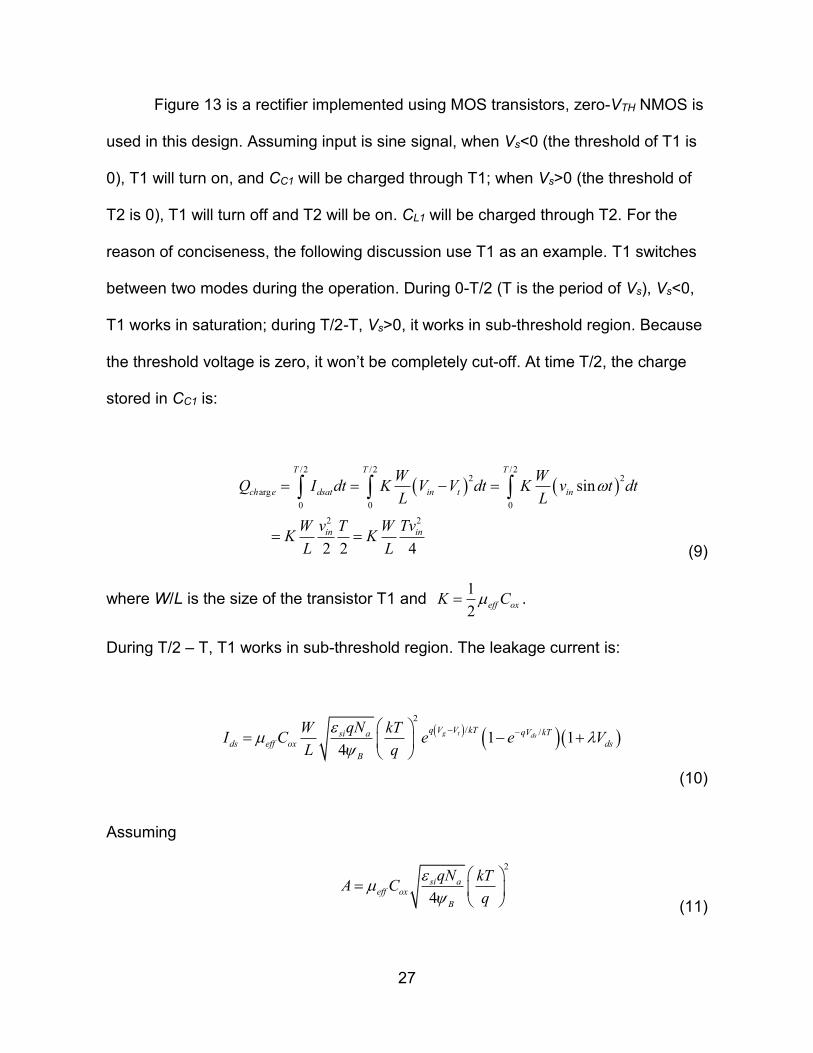
Figure 30 ........................................................................................................................ 57
Figure 31 ........................................................................................................................ 59
Figure 32 ........................................................................................................................ 61
Figure 33 ........................................................................................................................ 64
Figure 34 ........................................................................................................................ 66
Figure 35 ........................................................................................................................ 71
Figure 36 ........................................................................................................................ 71
Figure 37 ........................................................................................................................ 75
Figure 38 ........................................................................................................................ 77
Figure 39 ........................................................................................................................ 78
Figure 40 ........................................................................................................................ 81
Figure 41 ........................................................................................................................ 82
Figure 42 ........................................................................................................................ 85
Figure 43 ........................................................................................................................ 86
Figure 44 ........................................................................................................................ 86

x
Figure 45 ........................................................................................................................ 89
Figure 46 ........................................................................................................................ 90
Figure 47 ........................................................................................................................ 92
Figure 48 ........................................................................................................................ 93
Figure 49 ........................................................................................................................ 96
Figure 50 ........................................................................................................................ 96
Figure 51 ........................................................................................................................ 97
Figure 52 ........................................................................................................................ 98
Figure 53 ........................................................................................................................ 98
Figure 54 ........................................................................................................................ 99
Figure 55 ........................................................................................................................ 99

1
CHAPTER 1
INTRODUCTION
1.1 Motivation
Wireless sensor is a device which can be used to monitor the physical or
environmental conditions, such as pressure, temperature, humidity, etc. It can collect
data and send them back to the reader which can be a smart phone, tablet,
computer, or any other electronic devices. At present, wireless sensors have been
used in a wide range of applications. Some examples are discussed as follows. In
medical service area, wireless sensors can be used to monitor body temperature,
blood pressure, heart beating rate, and other health related data. They can also send
the data to the doctors to monitor the patients’ health conditions. In civil structure
health monitoring applications, the sensors can be used to detect the corrosion of
metals, and can help determine maintenance schedule of the buildings. In
commercial area, people can use the sensors to monitor the storage environment,
such as temperature, humidity, oxygen density, etc., to keep the environment
suitable for commodity storage. In manufacture industry, wireless sensors can be
used to monitor and control various aspects of the manufacture process to achieve
near zero down time operations.
Because of these emerging applications of wireless sensors, the demand for
wireless sensors increases rapidly. Figure 1 shows the revenue of wireless sensor
market from 2002 to 2012 [1], which clearly indicates that the exponential growth of
wireless sensors.

2
Figure 1.The market of the wireless sensor from 2002 to 2012 [1]
Some common characteristics of wireless sensors are low power, miniature
size, and low cost. Such devices can be powered by batteries or obtain energy from
external environment using energy harvesting circuits. The former is often referred
as active sensors and the latter is called passive sensors. In both types of sensors,
low power is extremely desirable. For active sensors, low power consumption
increases sensor operating cycles and also reduces battery size. For passive
sensors, low power consumption is a permanent requirement since the available
energy is typically very limited. The sources for passive sensor devices to harvest
energy include thermal, electromagnetic field, motion, etc. Currently a popular
energy harvest approach is to acquire the energy from Radio Frequency (RF) waves,
which is also the carrier of the sensor communication signals. For passive wireless
sensors with RF energy harvesting function, two of the most critical factors that affect
the level of harvested energy from the RF signal are operation distance and antenna
size. A short distance and a large antenna help obtain more energy. Figure 2 shows
experiment data from Berkeley [2], which indicates that the power loss rate increases

3
with the operating distance. However, longer operating distance and smaller antenna
size are much more preferred in the application of wireless sensors. If we could
reduce the power consumption of wireless sensors, then they can operate in
relatively longer distance with a smaller antenna.
Figure 2. The loss rate of electromagnetic filed energy with distance [2]
Figure 3. The typical structure of passive wireless sensor
1.2 Objectives
Rectifier
Regulator ADC/RDC
LDO
Digital Control
Modulation
Demodulation
VDC VDDA
VDDD
Sensors
Antenna
RF

4
Figure 3 shows a typical structure for a passive wireless sensor with RF
energy harvesting function. It consists of energy harvest circuits (antenna, rectifier,
regulator), analog circuits (Low-Drop Output (LDO) regulator), analog to digital
converter (ADC)/resistance to digital converter (RDC)), digital circuits (digital control
and memory), modulation and demodulation circuits. The circuits that consume most
of the power are the three blocks, regulator, Analog to Digital Converter (ADC)/
Resistance to Digital Converter (RDC) and Low-Drop Output (LDO) regulator, which
are shaded in Figure 3. They are also the three circuits that are investigated in this
research. The antenna acquires the energy from the external electromagnetic field.
However, the voltage at the antenna is an AC voltage with a small amplitude, which
can't be used as power supply for other circuits. The rectifier converts the low AC
voltage at the antenna to a higher DC voltage and sends it to the regulator. Because
the output of the rectifier is noisy and has a large variation according with the input
power and the load current, it's also unsuitable to be used as power supply. Thus, a
regulator is needed to generate a stable and clean power supply for other circuits
from the rectifier. The ADC/RDC is used to measure the electrical signal of the
sensor, such as resistance value in this example, and converts it to digital data. The
digital circuits acquire the information and send the data back to the reader via a
back scatter scheme [42], which is implemented by the modulation and the antenna.
The LDO regulator is usually to satisfy the different power supply requirements for
different circuits. Usually, the digital circuits prefer to operate with a lower power
supply voltage than the analog circuits. This helps to reduce power consumption in
the digital circuits. Meanwhile, the analog circuits need a clean power supply to

5
minimize the power supply noise impact. As discussed above, regulator, ADC and
LDO are three important analog building blocks in wireless sensors. Meanwhile, they
are among the most power hungry circuits in passive wireless sensors. Hence, this
research intend to investigate low power low voltage design techniques for these
circuits.
1.3 Major contribution of the research
In this dissertation, we present low power circuit design techniques for voltage
regulator and resistor to digital converter (RDC) circuit which could be integrated on-
chip in Radio-Frequency Identification (RFID) sensor applications. The proposed
work is a part of integrated efforts in the development of a RFID sensor, which is
used to measure the impedance of a Sol-Gel chemical sensor [58] in building
corrosion detection applications. The proposed voltage regulator has simple circuit
structure and near zero DC current dissipation (except the current drained by its
load). The resistor to digital converter (RDC) consists of a cascaded current mirror, a
reference resistor, and a CR SAR ADC circuit with 9-bit resolution. The proposed
design techniques eliminate the need of dedicated voltage reference in the ADC
circuit and reduce the size of the ADC capacitor array by half compared to traditional
CR SAR ADCs with the same resolution. The proposed techniques also significantly
reduce the circuit power consumption with enhanced measurement accuracy. The
proposed low power circuits and an optimized voltage multiplier based RF energy
harvesting circuit (for powering the proposed circuits) are implemented in a 0.13µm
CMOS technology. The functionality and performance of the proposed circuits are

6
demonstrated by both of simulation and measurement results. All the circuits could
also be used in other similar wireless sensing circuits.
In addition, a low power CR SAR ADC which can correct the parasitic
capacitance error with little hardware and energy overhead is designed [3]. SAR
ADC is the most used ADC topology in low power circuits, which features low power
consumption, moderate conversion speed and moderate accuracy. For CR SAR
ADC, the main power consumption is due to charging the capacitor array. To
minimize the power consumption, a separate small capacitor can be used to replace
the capacitor array to sample the input voltage. This type of ADC is called as SAR
ADC-S2C (successive approximation register analog to digital converter with
separate sampling capacitor) in the low power design. However, SAR ADC-S2C will
suffer from the error induced by the parasitic capacitance of the capacitor array. By
avoiding the charge sharing between the capacitor array and the parasitic
capacitance, the proposed ADC reduces the error associated with the parasitic
capacitance. This research first compares the SAR ADC-S2C with the conventional
SAR ADC and analyzes the gain error caused by parasitic capacitance in SAR ADC-
S2C design. Although the gain error can be compensated by multiplying the ADC
output by a correction coefficient, it is achieved at the cost of reduced ADC input
range and requires a calibration process for determining the coefficient value. This
work presents an effective technique to minimize the effect of the parasitic
capacitance for the SAR ADC-S2C circuit. It requires negligible hardware overhead,
does not need calibration process and additional clock phases or cycles in ADC
conversion operations. In addition, the proposed technique is capable of addressing

7
not only the linear error caused by constant parasitic capacitance, but also the
nonlinear inaccuracy in the case that parasitic capacitance varies with the voltage
potential at the top plates of the CS capacitor array (similar as metal-insulator-
semiconductor (MIS) capacitor). Finally, the effectiveness of the proposed technique
is demonstrated by post-layout simulation results.
Furthermore, design techniques for low voltage LDO circuits are also
investigated. To address the challenge of traditional LDO design not suitable for
ultra-low voltage operation, a digital loop LDO regulator is proposed, whose power
supply can be scaled to 0.7V. Its power consumption and efficiency are also superior
to that of analog design. Compared to existing low-voltage digital LDO design, the
proposed circuit improves the line and the load response time with minimum
hardware and power overhead. The regulator response time is improved by more
than three times and the ripple is significantly reduced. The start-up time is also
improved. The circuit analysis are provided to explain the improvement by the
proposed design. The proposed circuit is implemented using a 0.18µm CMOS
technology and simulation results are presented to validate the performance
improvement.
1.4 Organization of the thesis
The reset of the thesis is organized as follows. Chapter 2 surveys the related
work that are reported in recent literature. Chapter 3 presents the developed low
power circuit design techniques for a RFID sensor circuit. The developed parasitic
error reduction technique for SAR ADC circuit are described in Chapter 4. Chapter 5

8
presents the developed ultra-low voltage digital LDO circuits. Finally, conclusions
and future work are discussed in Chapter 6.

9
CHAPTER 2
RELATED WORK IN WIRELESS SENSOR CIRCUIT DESIGN
2.1 Recent development of low-power RFID sensors
RFID (radio-frequency identification) was initially developed as an alternative
to the bar code for efficient and convenient inventory management. Later, some
sensing functions are integrated into RFID circuits and this leads to a new type of low
cost wireless sensors, which are commonly referred to as RFID sensors. Such
sensors could be classified to passive and active sensors by the using battery or not.
A passive RFID sensor does not need battery and it acquires the energy from the
external electromagnetic field. It has the features of low cost, long lifetime, wireless
access, battery-free and simple structure. These features make it more easily
deployed and keep it remain in operation for a long time. Due to these advantages,
passive RFID sensors are more preferred compared to active RFID sensor, which
requires battery but are capable of operating in relatively long distance. Recently,
some passive RFID sensing platforms which integrate multi-sensors, microcontroller
and ports are developed such as Intel WISP (wireless Internet service provider) [4].
Combining with these sensors, the RFID is able to be used in environment monitor,
building maintenance or structure conditions, and information collection applications.
But the cost of these platforms with multi-chips is high. Single chip RFID sensors are
more preferred in many applications.
Inspired by the wide applications of RFID sensors, significant research efforts
have been devoted to address the design challenges of the single chip RFID sensors
at both software and hardware aspects [5], [6], [7], [8], [9]. One of these stiff

10
challenges in the development of RFID sensing circuits is that the energy harvested
from RF signals is very limited. To address this challenge, different energy harvest
circuit designs have been proposed [10], [11], [12] and design optimization
techniques are investigated [13], [14], [15]. With the state of the art of circuit
techniques, the efficiency of RF energy harvest circuits is still low, ranging from 10%
to 20%. As a result, the physical sensing structure as well as the digital and analog
sensing circuits needs to have extremely low power consumption. In [10], an ultra-
low power RFID with the structure shown in Figure 4 is developed, which includes
voltage multiplier (rectifier), memory, control logic, modulator and demodulator. The
reading distance can reach 4.5- or 9.25-m at 500-mW ERP or 4-W EIRP base-
station transmit power, respectively, at the operating in the 868/915-MHz ISM
(industrial, scientific and medical) band with an antenna gain less than 0.5dB. There
are no external components except for the printed antenna, which reduces the cost
of the tag. The tag information can be read by the integrated memory. However,
because there is no any sensor or sensor connection port integrated in the tag, the
application of this RFID tag is quite limited, and it can’t be used for the information
collection application.
Low-power analog circuits, including voltage level detection circuit with 900nA
current dissipation [12] are reported with the structure in Figure 5. It uses the
recovered clock from the input wireless signal as a reference in the counter to
convert the analog signal to digital code. This works as a clock counter based ADC
to convert the analog signal to digital code. It makes the sensor tag flexible
compared to that in [10]. It's possible to be used to measure the sensor signal and

11
send the data to the reader. But in this circuit, the ADC can't be used to measure the
resistance of sensors directly. The ADC can only be used to measure the voltage
level. Thus, it needs an accuracy biasing circuit to convert the resistance of sensors
to voltage level. It is not easy to achieve this in passive RFID circuit. Because of
using the recovered clock as the reference, the resolution of the ADC is limited. Only
5-bits resolution is achieved in the circuit reported in [12]. The operating distance of
this device is more than 18 meters under 7W base power station with a 50Ω
commercial antenna which is much larger than the printed antenna in [10].
The voltage regulators with 110nA DC current [16] and 300nA DC current [17]
are proposed respectively. Although conventional circuit topologies are used in this
designs, the circuits are highly optimized to address the low-power design
challenges in RFID sensors. Also these circuits have complex structures and it may
be difficult to make the circuits stable in the entire operation range of the passive
RFID circuits. Usually they need some auxiliary circuits to help the regulator work
continually. With the push to extend the operating distance of RFID sensors (hence
less RF energy delivered to RFID sensors) and the use of RFID devices in more
capable sensing applications, novel integrated circuits with ultra-low power design
techniques are strongly needed.

12
Figure 4. RFID tag proposed in [10]
Figure 5. RFID tag proposed in [12]
Figure 6. The single-end SAR ADC proposed in [23]

13
2.2 Low-power SAR ADC
The charge scaling successive approximation register (CS SAR) ADC is an
attractive design choice for low-power ADC implementations [18] [19]. They are more
suitable for wireless sensor circuits. Recently, quite a few low-power CS SAR ADC
circuits have been reported [20] [21] [22] [23]. Many of them are designed to operate
with single-ended signals to achieve better power efficiency. The low-power
advantage and the existence of a large number of sensor devices with single-ended
outputs [24] make the use of single-ended ADCs appealing in many low power
applications [24] [25] [26]. To reduce the power consumption of the driver circuits,
SAR ADC designs using separate sampling capacitors are reported [23] [24] [25] [26]
[27] as shown in Figure 6. It uses a small capacitor to sample input voltage and
compares the sampled output with the voltage generated by the charge scaling (CS)
capacitor array. This SAR ADC topology will be referred as SAR ADC-S2C structure
(S2C stands for separate sampling capacitor). This ADC structure is more suitable for
some sensor measurement, in which no differential signals are available. Despite its
low-power advantage, SAR ADC-S2C design suffers from gain error and reduced
input range caused by the parasitic capacitance in the CS capacitor array.
Previously, several techniques have been developed to address the effects of
the parasitic capacitance in different SAR ADC designs. In [28], the bottom plate
parasitic capacitance of a C-2C capacitor array is shielded by a metal layer, and the
metal layer’s potential is driven by a second C-2C capacitor array operating similarly
as the main capacitor array. This technique works well for capacitor arrays with large
unit capacitance values, but increases the total capacitor area and the energy

14
dissipated by the capacitor arrays. The shielding technique is also used in [29] [30] to
minimize the effects of parasitic capacitance at the floating node of the CS capacitor
array. In [29], the potential of the shielding layer is switched between the reference
voltage and ground; while a dedicated voltage generator is used to control the
potential of the shielding layer in [30]. The techniques of using configurable
capacitance banks are reported to compensate the effect of parasitic capacitance in
both split-capacitor array SAR ADC design [31] and fully differential ADC [32]. An
SAR-ADC auto-calibration technique is presented in [33], which compensates the
inaccuracy factors by injecting charge to the floating node of the capacitor array. The
charge injection is achieved by using a calibration capacitor that is driven by an
analog voltage determined during the calibration process.
The design in [34] includes parasitic capacitance as a part of the capacitance
to be implemented in the array. To cope with variations associated with parasitic
capacitance, a combination of capacitance bank based coarse-level calibration and
an analog voltage controlled fine-level calibration is utilized to trim the capacitance of
each branch to the desirable value. In addition to the above circuit techniques,
general error models for SAR ADC circuits are developed [35] [36] and various digital
compensation techniques have been proposed [37] [38] [39]. Nevertheless, the
previously proposed techniques either are not suitable for the SAR ADC-S2C
structure or require large hardware overhead and lengthy calibration processes.

15
Figure 7. Digital LDO proposed in [40]
2.3 Ultra-low voltage digital LDO
LDO regulator is widely used to provide constant power supply to other
circuits. In wireless sensors, it is mostly used to provide the power supply for digital
circuits and digital memory, since separate power supplies are preferred for digital
and analog circuits to minimize the impact of digital switching noise on analog
circuits. And lower power supply is preferred to reduce the digital power
consumption. Traditional analog LDOs consume more power and their stability has
to be considered carefully. Moreover, with the scaling down of power supply voltage,
the design of analog LDO becomes more challenge partially due to the difficulty of
high gain amplifier design with low supply voltage. To address this problem, digital
LDO circuits are reported in recent literature. In [40], a digital LDO is proposed as
shown in Figure 7. It uses a PMOS array to provide the load current and control the
output voltage. The SAR logic is used to generate the digital control code for the
PMOS array. This makes the circuit easy to be set stable, and the operation power
supply can be as low 0.6V. However, the response time to the variation of the line

16
and the load is inversely proportional to the resolution of the PMOS array in this
design. If the resolution is increased to reduce the ripple at the output, and then, the
response time also increases. On the other hand, the resolution is reduced to
achieve shorter response time, the ripple at the output will be large and the static
current will also increase. Thus the efficiency of the LDO will decrease. The start-up
response is also very slow when the resolution is high. As a compromise of these
considerations, 256 PMOS devices, corresponding to 8-bit resolution, are used in the
array [40] to avoid long start-up and response time. Other implementations based on
this structure are also reported in [45][46][47][49][52] for various applications. But
they need either load detection or calibration circuits which are complex for most
wireless sensor designs.
Figure 8. Digital loop LDO proposed in [41]
Another digital loop LDO as shown in Figure 8 is reported in [41]. It uses two
voltage control oscillators (VCO) as the error amplifier (EA), and uses phase
frequency detector (PFD) to generate the pulses for controlling the charge pump

17
(CP). After the Low-Pass Filter (LPF), a stable output voltage will be generated at the
gate of the Power MOS. Then the output Vo will also be stable. The loop is designed
using digital circuits which enable it to operate under 0.6V power supply. The loop is
also easier to be set stable compared to its analog counterpart. But the response of
the line and load variation are still slow for certain applications, especially when the
power consumption is low.

18
CHAPTER 3
LOW POWER ANALOG CIRCUIT DESIGN FOR RFID
SENSING CIRCUITS
3.1 System overview
As shown in Figure 9, the RFID Sol-Gel sensor system under investigation
consists of an antenna, a CMOS IC chip, and a Sol-Gel sensing device. The Sol-Gel
sensor used in the system is a type of specially synthesized ceramic oxide glass. Its
electrical conductivity (or resistance) is affected by chloride ions concentration, and
thus the conductivity change can reflect structure corrosion conditions when the
sensors are attached to the metal in certain locations of the structure to be
monitored. From the electronic design perspective, the Sol-Gel sensor can be simply
treated as a conductive component, whose resistance needs to be measured.
Fig. 9. Block diagram of the RFID sol-gel sensor
The rectifier and regulator compose the energy harvesting circuit. The rectifier
in the IC chip harvests the RF energy from the antenna and converts the RF voltage
CMOS IC

19
to a DC voltage. Because of the integration of the measurement circuits (the RDC
circuit) in this chip, the current from the rectifier circuit is not large enough to support
the rest circuits operating in long time term. A large on-chip capacitor is used to
accumulate the harvested energy for continuous operation; and the sensing
operation starts only after enough energy is accumulated. The ready state is
determined by the standard that if the voltage across the capacitor exceeding 2.2V.
The capacitor also functions as a low pass filter. The regulator circuit provides a
constant voltage around 1.2V to power the rest RFID circuits. The RDC is the
measuring circuit to sense the resistance of the Sol-Gel sensor and digitize the
measured resistance into a 9-bit digital data, which will be sent back to RFID reader
via back-scattering techniques [42]. The rest circuits in the IC chip, including the
digital control, demodulation and antenna impedance modulation circuit, are similar
to the corresponding circuits in a typical RFID tag [10].
3.2 Rectifier design
Passive RFIDs harvest the energy from the electrical-magnetic (EM) field.
According to the coupling techniques, it can be classified into two types, near field
and far field RFID. Most near-field tags rely on the magnetic field through inductive
coupling to the coil in the tag. This mechanism is based upon Faraday’s principle of
magnetic induction. A current flowing through the coil of a reader produces a
magnetic field around it. This field causes a tag’s coil in the vicinity to generate a
small current. For this type of RFID, the operation range is usually less than 1m, so
its application is highly limited.

20
Far-field passive RFID sensors usually operate in 860–960 MHz UHF (ultra-
high frequency) band or in 2.45 GHz Microwave band. Far-field coupling is
commonly employed for long-range (5–20 m) RFID. In contrast to near-field, there is
no restriction on the field boundary for far-field RFID. The EM field in the far-field
region is radioactive in nature. Part of the energy incident on a tag’s antenna is
reflected back due to an impedance mismatch between the antenna and the load
circuit. Changing the mismatch or loading on the antenna can vary the amount of
reflected energy, which is the technique called backscattering. The attenuation of the
EM field in far-field region is proportional to 1/r2, where r is the distance between the
RF signal transmitter and receiver. This is smaller by orders of the magnitude than in
the near-field range (which is 1/r6). An advantage of a far-field tag operating at a high
frequency is that the antenna can be small, leading to low fabrication and assembly
costs. Small size is also preferred for easy deploying. Due to the advantages of the
long operation distance, low cost and small size, the far field passive RFID technique
is more suitable for wireless sensor applications.
S
RinVin VsVin
Rant
Rin
Figure 10. The simplified model for passive RFID system analysis in [43]
Figure 10 shows a simplified circuit model for a far-field passive RFID system
[43]. It consists of the reader and the tag. The tag antenna is modeled by 𝑣𝑠 and

21
𝑅𝑎𝑛𝑡, the rest circuits of the tag are simplified to 𝑅𝑖𝑛. According to the coupling
principle of far field RFID, the peak voltage on the antenna of the tag, 𝑣𝑠,𝑝𝑒𝑎𝑘, could
be represented by [43]:
, 2 2s peak a ANTv P R p (1)
where 𝑃𝑎 is the power acquired by the antenna of tag and 𝑝 is the polarization
mismatch. It shows that 𝑣𝑠,𝑝𝑒𝑎𝑘 is determined by the available power (related to the
power sent out by the reader, the distance and the size of the antenna) and the
resistance of the antenna. The resistance of the antenna is usually limited by the
polarization mismatch. It is usually 50Ω or 75Ω. So the amplitude of 𝑣𝑠,𝑝𝑒𝑎𝑘 is small
and it's an AC voltage which can't be used as power supply for other circuits. To
convert the AC voltage to a DC value and boost it to a higher voltage level which can
serve as power supply for other circuits, a voltage multiplier rectifier is often needed
in passive RFID tag design.
GND
GND
Vs
Cload
VDC
CC1D1 CL1
CL2
Figure 11. Dickson's voltage multiplier in [44]
D2

22
I Principle of rectifier
The most common voltage multiplier rectifier is the Dickson’s voltage multiplier
shown in Figure 11 [44]. Vs is the sine wave from the antenna. When Vs < 0, and its
absolute value is larger than the threshold voltage of the diode, D1, CC1 will be
charged through D1; when Vs > 0 and its absolute value is larger than the threshold
voltage of the diode, D2, then CL1 will be charged by CC1, via diode D2, CL1 won’t be
discharged. Similar, CL2 and other capacitors will be charged to higher voltage, and
the output voltage can be derived as [44]:
𝑉𝑂 = 𝑀(𝐶
𝐶+𝐶𝑃𝑉𝑠,𝑝𝑒𝑎𝑘 −
𝐼𝑜
𝑓(𝐶+𝐶𝑃)− 𝑉𝑇𝐻) − 𝑉𝑇𝐻 (2)
where M is the number of stages, VTH is the threshold voltage of the diode, f is the
input frequency of VS, CL = CC = C and CP is the parasitic capacitance of the diode.
As the value of the expression inside the brackets is positive, the output voltage
could be boost to a higher voltage which can be used by other internal circuits. In
CMOS circuits, the diodes are typically implemented by MOSFET with diode
configuration. Then body effect will affect VTH values and such impacts is not
included in Equation 2. Because of the body effect, VTH increase with the output
voltage. As output is high to certain level, the value of the expression inside the
brackets will become 0 and hence adding additional stages will not further increase
Vo. So there is a maximum value for the output voltage.
The efficiency of the rectifier is defined as:

23
𝐸𝑓𝑓𝑖𝑐𝑖𝑒𝑛𝑐𝑦 =𝑉𝑜×𝐼𝑙𝑜𝑎𝑑
𝑃𝑎𝑣𝑎𝑖𝑙𝑎𝑏𝑙𝑒 (3)
Where Iload is the load current and Pavailable is the available power for the rectifier.
According to Equation 2 and 3, the efficiency is mainly determined by Vs,peak, VTH, CC
and Cp. Large Vs,peak and small VTH is preferred to improve the efficiency. In passive
RFID tag design, Vs,peak is affected by the available power, distance to the reader,
matching and the size of the antenna. To make the rectifier impedance match with
the antenna, an inductor are often used in the rectifier design [45] [46] [47], which
also helps boost the voltage to the rectifier to improve the efficiency of the rectifier.
Another solution to increase the rectifier energy harvesting efficiency is to reduce
VTH. Several technologies have been proposed to reduce VTH in the rectifier. In [48],
a static threshold voltage compensation circuit has been used. In [49], the charge
pump rectifier is built by low threshold diodes. However, this is difficult to be
integrated in standard CMOS process. Dynamic threshold voltage, VTH, cancellation
circuit has been also proposed in [59]. However, this circuit is complex and its
impedance is difficult to control. One of the most popular technique in latest RF
energy harvesting circuits is to use zero-threshold voltage transistor or low threshold-
voltage transistor to replace the diode. This not only significantly simplifies the
energy harvesting circuit design and analysis, but also improves the energy
harvesting impedance matching and efficiency. More importantly, many CMOS
technologies already support zero-threshold devices (intrinsic transistor). Thus, such

24
design can be implemented using only CMOS technologies. In the following sections,
RF energy harvesting circuit are analyzed.
II Impedance matching and inductor boost design
In the impedance matching analysis, the RF energy harvesting circuit can be
modeled by the circuits in Figure 12 [50]. Rant is the resistance of the antenna; LA is
the inductor used to compensate the imaginary part of the tag; RL represents the
non-radiating antenna resistance and the loss on interconnecting from antenna to
chip. Rin and Cin are the input resistance and capacitance of the chip. The impedance
of the matching network, I/O Pads, wire components and PCB trace are included in
Rin and Cin.
Vin Rin
Rant+RL
LA
Cin
i
+
_Vs
Vin
Ric
Cic
+
_
LA
Rant+RL
Vs
Figure 12. Circuit model used in impedance analysis in [50]
According to Figure 12, the peak value of voltage Vin can be derived as:
, ,
22
inin peak s peak
in ANT L ANT L
Rv v
R R R LQ L R R Q
, (4)
LA LA
Rant +RL Rant +RL

25
where Q is the quality factor of the tag chip. Q is defined as:
Qtag=[ω.(stored energy/dissipated energy)]=2
2
in in
in in
in
in
v j CC R
v
R
(5)
In the case that impedance is perfectly matched, we have:
2 1
inANT L
RR R
Q
(6)
2
2 1
in inANT
R CL
Q
(7)
Substituting Vs,peak by Equation 1, and using the impedance matching conditions
given by Equation 6 and 7. Vin,peak can be derived as:
22
, ,
11
2 2
ANT aviable
in peak s peak
R P QQv v
(8)
Since high Vin,peak value helps improve the efficiency of the rectifier circuit, large Rant
and Q are preferred in passive RFID design. However, as described in the previous
section, Rant is limited by the antenna polarization mismatch and its value is usually
constant (50Ω or 75 Ω). Moreover, Q value is also limited by the bandwidth of input
RF signal. According to the established standard [51], the operation frequency for
RFID are 865-868MHz in Europe and 902-928MHz in US. This limits the bandwidth

26
of the RFID interrogation signal to be less than 20MHz. So Q is limited by the signal
bandwidth for communication. And in Equation 8, Q is affected by Rin and Cin,
because that Rin is equal Rant in the matching condition. Q can only be adjusted by
Cin
The Rin and Cin in Figure 12 include the contributions from PCB trace, pins,
bonding wires, matching network and rectifier. Since the impacts of the pin and bond
pads are difficult to control, their values should be minimized. Thus the minimum size
pad is preferred and the bond wire need to be short. To design the impedance
matching circuit and rectifier separately, the impacts from the resistance and the
capacitance of the rectifier, Rrect and Crect, should be minimized, implying that large
rectifier resistance and small rectifier capacitance are preferred. In this case, the
impedance matching will be mainly determined by the matching network, which is
independent on the rectifier design. This arrangement simplifies the circuit design.
GND
GND
VsCC1
T1
CL1
T2
Figure 13. A single stage MOS rectifier circuit
III Rectifier efficiency in steady state
CL1 CC1
27
Figure 13 is a rectifier implemented using MOS transistors, zero-VTH NMOS is
used in this design. Assuming input is sine signal, when Vs<0 (the threshold of T1 is
0), T1 will turn on, and CC1 will be charged through T1; when Vs>0 (the threshold of
T2 is 0), T1 will turn off and T2 will be on. CL1 will be charged through T2. For the
reason of conciseness, the following discussion use T1 as an example. T1 switches
between two modes during the operation. During 0-T/2 (T is the period of Vs), Vs<0,
T1 works in saturation; during T/2-T, Vs>0, it works in sub-threshold region. Because
the threshold voltage is zero, it won’t be completely cut-off. At time T/2, the charge
stored in CC1 is:
/2 /2 /2
2 2
arg
0 0 0
2 2
sin
2 2 4
T T T
ch e dsat in t in
in in
W WQ I dt K V V dt K v t dt
L L
v TvW T WK K
L L
(9)
where W/L is the size of the transistor T1 and 1
2eff oxK C .
During T/2 – T, T1 works in sub-threshold region. The leakage current is:
2
/ /1 1
4
g t dsq V V kT qV kTsi a
ds eff ox ds
B
qNW kTI C e e V
L q
(10)
Assuming
2
4
si aeff ox
B
qN kTA C
q
(11)

28
The Ids equation can be simplified as:
2
/ /1 1g t ds
q V V kT qV kT
ds ds
kTI A e e V
q
(12)
So the charge leakage loss due to this leakage current is:
/ /
/2 /2 /2
/ /
/2
1 1
1 1
t ds
t ds
T T T
qV kT qV kT
leakage leakage sub sub ds
T T T
T
qV kT qV kT
sub ds
T
WQ I dt I dt Ae e V dt
L
WAe e V dt
L
(13)
since , sin ' 0.1in in peakv v t V ,
/1 1dsqV kT
e
, when
, sin ' 0.1in in peakv v t V
1 1sub dsV , Equation 13 can be approximated as:
,
/ /
/2
'
/ /
/2 '
/
2
/,/ 2 '
1 1
1 1
2
0.11 1 1
t ds
t ds
t
in peakt
T
qV kT qV kT
leakage sub ds
T
t T
qV kT qV kT
sub ds
T t
qV kT
qv kTin peakqV kT f t
sub
in in
WQ Ae e V dt
L
WAe e dt V dt
L
W TAe
L
vW kTAe e e
L v qv
(14)
According to the charge conversation, the following relation holds in the stable state.

29
argch e leakage load P CQ Q I T C C v (15)
argch e leakage load
P C
Q Q I Tv
C C
(16)
where Cp is the parasitic capacitance of the transistor, Iload is the load current, ∆v is
the increase of the output voltage at a single stage. Cp is the transistor parasitic
capacitance, it will be affected by the gate voltage of the transistor. It can be
simplified to linearly change with the input voltage. It can be approximated as:
2
1
2 1 2 /
oxaverage ox
ox in si a
WLCC WLC
C V qN
(17)
Based on above equations, the output voltage of the single stage can be derived.
Ignoring the body effect, each stage of the rectifier in Figure 13 has the similar output
voltage and the number of stages will not impact the efficiency.
IV Rectifier in impedance matching
As described above, to enable separate optimization for matching network
and the rectifier efficiency, the resistance and capacitance of the rectifier, Rrec and
Crec, should be ignored, which means that the effect of Crec and Rrec should be
minimized. If Crec is small and Rrec is large, the impedance of the tag is mainly
determined by the matching network. To reduce Crec, the size of the transistor should

30
be small. Meanwhile, a small transistor size also helps increase Rrec. But according
to the previous analysis in the rectifier efficiency, this may reduce the efficiency of
the rectifier.
Z ReCe
Figure 14. Equivalent circuit in rectifier impedance matching analysis [50]
To simplify the analysis, we take single stage rectifier in Figure 14 as the
example [50]. Cp is the parasitic capacitance of the transistor and R is the equivalent
resistance of the transistor; Ce and Re are the equivalent capacitance and resistance
of the rectifier respectively. We have:
2 2
1 12
1
2
1
1
22e
1
11 1
2 2R 2 2
1 4 12 2
2 2 2R
1 4 12
2
2
P Pe
P P
e P
P
P
P
C CR R R
C Cf C
C CfCR
R C CC C C C C
CfCR
C
CC
C C
(18)
where
CL CL

31
1
1 1
mn ox in
RWg
C VL
(19)
For multistage rectifier, the Re and Ce expressions are:
2
1 12
2
2
Pe
Pe
P
R CR
N C
CCC N
C C
(20)
where N is the number of the stages in the rectifier. To achieve small Ce and large
Re, W/L could not be too large. The number of stages, N, also affects the values of
Ce and Re. Large N will reduce Re and increase Ce. Thus in the design of high
efficiency rectifier, the size of the transistors and the number of stages should be
considered in the impedance matching. With these considerations, an eighteen-
stage voltage multiplier is implemented as shown in Figure 15 in this design. The
zero-threshold voltage transistors and 0.5pF metal-isolate-metal (MIM) capacitors
are used. The rectifier could convert the 50mV AC input to the 2V DC voltage with
the load around 10uA; or 200mV AC input to the 2V DC voltage with the load around
20uA. Since the load current is not large enough for some applications, a large
capacitor is used at the output of the rectifier to store the energy and provide the
additional power to other circuits for continuous operation.

32
Figure 15. Optimized 18-stages rectifier
3.3 Low power regulator design
Figure 16. Proposed regulator circuits
The regulator in the RFID is used to generate a stable and clean power supply
for the rest of the circuits. The proposed regulator circuit is shown in Figure 16. Its
M5
Vs
T1
T
2
CC
1
CL1
CL2
CC
2 CTank
N=18
CTank

33
input is provided by the rectifier which could be considered as the current source, Iin,
charging the capacitance tank, CTank. VDC is the voltage at the top of CTank. It works
as the power supply of the regulator circuit. Initially, there is little charge stored in the
capacitor tank and VDC is low. Transistors M2 and M3 are off and VB, the voltage
across capacitor C2, is low. Consequently, the output of INV3 is logic ”1”, which
closes switch S1 to charge capacitor C1 via M3. Meanwhile, switch S2 is open to
disconnect regulator load circuit from the source terminal of M4. When the rectifier
circuit starts to charge the large capacitor, CTank, VDC will increase gradually. At the
point that VDC increases to the voltage level 2·Vt, where Vt is the threshold voltage of
NMOS devices, transistors M1 and M2 turn on and capacitor C2 starts to be charged.
The voltage of C2 is:
𝑉𝐵 = 𝑉𝐷𝐶 − 2 × 𝑉𝑡 (21)
The parasitic effects (mainly body effect) and the impacts of the charging current are
ignored in this equation, since they are insignificant. With proper transistor sizing, the
gate threshold of INV1 is designed to be two thirds of its power supply voltage VDC.
Thus, when VB reaches 2/3VDC, the output of INV3 switches to ground, consequently
turning off S1 and closing S2. From the above relation and Equation 21, it is easy to
see the output of INV3 switches to ground when VDC = 6·Vt (which is about 2.2V for
the selected CMOS technology). After S1 is open, VC1, the voltage across capacitor
C1, is kept at the level of 5·Vt. Hence, as long as input voltage VDC is larger than VC1 -
Vt, assuming M4 has the same threshold voltage Vt, the regulator output voltage is:

34
𝑉𝑑𝑑 = 𝑉𝐶1 − 𝑉𝑡 −𝐼𝑙𝑜𝑎𝑑
𝑔𝑚4= 4𝑉𝑡 −
𝐼𝑙𝑜𝑎𝑑
𝑔𝑚4 (22)
where Iload is the regulator load current and gm4 is the transconductance of M4. If gm4
is large enough (by having large size), the above Vdd expression can be simplified to
Vdd = 4·Vt, which is constant. Note that transistor M5 is used to pull voltage VB to VDC
level after S1 is switched off. This eliminates the static current dissipation of the
inverter circuits. So the applicable energy for the load is Vt·(CTank + C2).
In this regulator circuit, the output voltage will be mainly affected by following
factors: input and output currents, leakage current and parasitic effects. To simplify
the derivation, the following assumptions are applied in the analysis: (1) M1, M2 and
M3 has the same threshold voltage ( 1tV ) and size ( 1W , 1L ), (2) 1
11
2
1=
L
Wck ox , (3) the
threshold voltage of M4 is 2tV , its size is 2
2
L
W and
2
22
2
1=
L
Wck ox , (4) CCC == 21 . In
the investigation of the impacts from the input and output currents, the parasitic
capacitance and the leakage current is ignored first. 1CV can be approximated in
terms of overdrive voltage odC VV 5=1 , where 1
31=
k
IVV tod , 3I is the current
charging to C2. Also 1m
loadt
g
IV in Equation 22 can be substituted by
2
21 kV
IV
ds
loadt
. So Equation 22 could be rewritten as:

35
2
2
1
31
155=
kV
IV
k
IVV
ds
loadttout
(23)
Since the ratio of I1 and I3 is proportional to the capacitance values of CTank and C2, I3
can be derived as:
𝐼3 = 𝐼𝑖𝑛 × (𝐶
𝐶𝑇𝑎𝑛𝑘+ 2)
−1
(24)
And the voltage between the drain and the source of M4, Vds, is:
𝑉𝑑𝑠 = 𝑉𝐷𝐶 − 𝑉𝑜𝑢𝑡 (25)
In Equation 23, threshold voltages, Vt1 and Vt2, can be considered as constant which
are determined by the fabrication process. loadI represents the current consumed by
the rest circuits, which is also approximately constant. 3I is part of the input current
( inI ), and it depends on the energy acquired by the rectifier and the antenna. Its
value may varies with the change of the operating distance and the external
electromagnetic power. To make the output voltage less associated with the
operation environment, 1k and 2k should have large values.
Based on Equation 23, the line regulation rate (in
out
I
V
) and output regulation
rate (load
out
I
V
) can be derived as:

36
2
1
2
5==
1
1
Tank
in
in
out
C
CIk
I
VR (26)
loaddsload
out
IkVI
VR
2
21
1
2
1==
(27)
where 1R is the line regulation rate and 2R is the output regulation rate. Clearly,
large sizes of 31M (M1, M2 and M3 have the same size) and 4M are preferred to
reduce 1R and 2R . However, large size will induce more parasitic capacitance,
which reduces the efficiency and degrades the performance of regulator as
described later. So the sizes of 31M and 4M should be carefully optimized.
The leakage current impacts the regulator before and after enabling the
regulator output. Before INV3 switching to "0", the voltage at node B will increase
with DCV gradually. When it’s around the gate threshold voltage of INV1, both of the
PMOS and NMOS in INV1 will be in saturation. So a large short circuit current will be
dissipated by INVI. The maximum leakage current at the switching point is:
2313, 4= ttmaxleakage VVkI (28)
where 3k and 3tV are the parameters of the NMOS devices in INV1. Due to the
effect of the leakage current, the current 3I in Equation 23 and 24 can be estimated
by

37
1
max.3 2=
Tank
leakageinC
CIII (29)
According to Equation 23 and 29, the output voltage will be reduced by the leakage
current. If inleakage II >max. , DCV will not be able to reach 2.2V and the regulator will not
be able to enter its normal operation mode. So the channel length of the PMOS and
NMOS in INV1 need to be large to reduce maxleakageI , . In the design of the regulator,
INV1 has a small leakage current and INV2 has a sharp voltage transifer curve to
accelerate the model transition.
After the output voltage has been established at the output, the leakage
current will draw charge from the capacitors, CTank, C1 and C2, which makes the
output voltage and regulator efficiency reduce. Since the capacitor CTank is very large
and the leakage current from CTank is usually small, which is mainly caused by the
static current of the inverters, the impact of leakage current on charge tank voltage
VDC can be ignored. C2 can be considered as part of capacitor tank, so the leakage
current impact is similar to CTank and it can also be ignored. However, the output
voltage will be reduced by the leakage current associated with capacitor C1. Because
of the large size of 4M , a large discharge current on C1 will be generated by the
leakage at the gate of 4M . The tunneling leakage current density has been modeled
as [53] [54] [55]:

38
oxgoxggoxg
ox
auxg
n
ox
oxref
gDT VVtBT
VV
T
TAJ
tox
1exp=
2 (30)
where Bg hqA /8= 2 , hqmB Boxg /328= 3/2 , oxm is the effective carrier mass in
oxide, B is the tunneling barrier height, oxt is the oxide thickness, oxrefT is the
reference oxide thickness, and ausV is an auxiliary function which approximates the
density of the tunneling carriers. g , g , and g are the physical parameters
determined by the CMOS fabrication process. gV is the gate voltage of the
MOSFET device, ntox is a fitting parameter, and VOX is the voltage across the oxide of
the MOSFET device. This can be used to estimate the gate leakage of M4.
a. The coupling capacitors divider b.The small-signal model of 4M
Figure 17. The model of parasitic capacitance
Another issue in this regulator is the large parasitic capacitance induced by
the use of large 4M . A voltage divider will be generate by gsC , gdC and 1C as
C1
C1

39
shown in Figure 17(a). The small signal model of the circuit is shown in Figure 17(b).
The output voltage can be derived as:
load
gd
oddd
gd
gd
dc ICACAC
rCv
CACAC
CACv
11
= (31)
where A is the instrincs gain of the regulator transistor M4, odmbm rggA = , Ctotal
is the total capacitance at the gate of 4M , gdgstotal CCCC 1= . So the relationship
between the variations of Vdd and Vdc is:
1
=CACAC
CAC
dv
dv
gdtotal
gdtotal
dc
dd
(32)
If A is large enough and totalgd CCA >> , the above euqation can be simplified as:
𝑑𝑣𝑑𝑑
𝑑𝑣𝐷𝐶=
𝐶𝑔𝑑
𝐶𝑔𝑑+𝐶1 (33)
If gdCAC >>1 , we have:
𝑑𝑣𝑑𝑑
𝑑𝑣𝐷𝐶=
1
1+𝐴 (34)

40
According to Equation 32 - 34, if we want to reduce the impact of the
coupling capacitance on the output voltage, large A and 1C are preferred.
Increasing 1C is a better choice, since the high gain usually needs large 4M which
will also increases the parasitic capacitance. Figure 18 shows matlab simulations
with assuming 10=A . It shows that when DCV decreases by 600mV, ddV will
decrease by 60mV.
The proposed regulator design has a very simple circuit structure. It does not
require bandgap voltage reference, operation amplifier, unit-gain buffer and loop
compensation circuits that are normally used in previous traditional regulator designs
[16] [17]. Also, the proposed regulator itself has zero current dissipation after the
regulator output is enabled. Although the inverter circuits in the regulator design have
leakage current power consumption before the regulator output is enabled, their
power consumption is insignificant if the inverters are comprised of transistors with
very small (W/L) ratios.
The exact voltage level of the proposed regulator output is relatively sensitive
to process variations. However, the exact voltage level is not critical in this as well as
many other RFID sensing applications. This is because in many sensing applications
electrical parameter ratios are used to measure the interested variables and the
exact voltage values are often canceled in measurement expressions.
Instead of emphasizing on the exact regulator output level, a more important
design concern is to make the regulator output constant during sensing operations.
Three factors potentially cause small variations at the proposed regulator output.
One is the leakage current that discharges capacitor 1C analyzed in Equation 30.

41
Depending on the duration of sensing operations, the value of 1C need to be
selected sufficiently large and potential leakage paths associated with 1C should be
carefully examined in the layout design. The second factor is coupling capacitor in
Equation 31. The voltage variation at the regulator input may affect 1CV through the
gate-drain parasitic capacitance of M4. To minimize this, 1C need to be large. The
third factor is the variation of the load current as indicated by Equation 23. The
impact of this factor can be reduced by increasing the transconduction of M4, 4mg .
Also, the variation on loadI can be minimized by properly scheduling circuit
operations and circuit design techniques. For example, the digital circuits can be
disabled during analog sensing operations to prevent digital switching activities from
causing loadI variations. In addition, the analog sensing circuits can be designed to
always drain constant current when the measurement reading is taken. Such an
example is described in the following sub section.
a. R1 v.s. Iin with different k1 b. R2 v.s. Iload with different k4

42
c. Matlab simulation for Equation 32
Figure 18. Simulated regulator line and load regulation
3.4 Resistance to digital converter
Figure 19. Resistance to digital converter circuit

43
As shown in Figure 19, the RDC circuit is comprised of a cascoded current
mirror (M1 - M6), a reference resistance RREF, and a charge-redistribution (CR)
successive approximation register (SAR) analog to digital converter (ADC). The Sol-
Gel sensor, whose resistance is to be measured, is represented by resistor RSEN in
the figure. The resistance of the Sol-Gel sensor used in the project can vary in the
range of 200KΩ - 700KΩ. The current mirror controls the currents flowing through
RREF and RSEN. To minimize power consumption, the current (ISEN) of RSEN is
designed to be 1 µA. However, the current (IREF) of RREF is K times larger than (ISEN)
due to the following two reasons. First, IREF is used to charge the capacitor array of
the CR SAR ADC and a relatively large current reduces the charging time. Second,
the selection of a large IREF value allows using a small RREF value (and hence a small
silicon area) to achieve a desired voltage drop across RREF. For the convenience of
discussion, voltages applied at RREF and RSEN are denoted as VREF and VSEN,
respectively. VREF works as the reference voltage in the ADC, while VSEN works as
the input voltage. The ADC circuit digitizes the ratio of VSEN over VREF. Assume the
digital data of the ADC output is D. Then, the value of RSEN can be expressed as:
𝑅𝑆𝐸𝑁 = 𝐷 × 𝐾 × 𝑅𝑅𝐸𝐹 (35)
This equation also indicates that the power supply voltage level does not affect RSEN
measurement, which supports the previous discussions.
In this design, RREF is implemented using poly resistor that is available in the
selected CMOS technology. Due to its low temperature dependence coefficient,

44
temperature compensation is not needed to be considered in the current design. To
cope with the uncertainties on the realized RREF and K values due to process
variations and devices mismatches, a simple calibration can be performed after chip
fabrication. In the calibration process, instead of the Sol-Gel sensor, a high-precision
resistor with known resistance value is connected to the RDC circuit. From the
measured resistance, the actual value of K·RREF can be easily obtained from
Equation 35. The error on the realized K·RREF value is converted into a digital word
and stored in an on-chip fuse-based memory. Then, digital error compensation can
be performed either by the RFID circuit or by programs in the RFID reader. In the
current design, we take the latter approach to minimize the digital circuits on the
RFID chip.
When digitizing the ratio of VSEN over VREF, VREF and VSEN are fed the ADC
circuit as voltage reference and ADC input, respectively. A conventional design
constraint for ADC circuits is that the ADC input should be always smaller than the
voltage reference level. This constraint not only unnecessarily increases circuit
power consumption but also degrades resistance measurement accuracy. The
former is because the ADC capacitor array is charged to a high voltage level when a
high reference level is used to satisfy the above design constraint. The latter is
caused by the large voltage difference between the two output branches of the
current mirror. For example, if RSEN value varies from 200KΩ to 700KΩ and ISEN is 1
µA, the largest VSEN is 0.7 V. Then, VREF needs to be 0.7 V at least. However, with
this design configuration, when the Sol-Gel sensor resistance is at its low end
(200KΩ), the different between VREF and VSEN is about 0.5 V. Due to finite output

45
resistance of the current mirror, the ratio of IREF over ISEN will be impacted and,
hence, the measurement accuracy is degraded.
Figure 20. ADC sampling circuit with level-shifting capability
In the proposed RDC design, we eliminate the constraint, VREF > VSEN, by
using a novel circuit technique, which is sketched in Figure 20. In this figure, CS is
the sampling capacitor of the ADC circuit. During the sampling operation, the two
terminals of the capacitor are connected to VREF and VSEN in the design respectively.
After the sampling operation, the ADC comparator first compares VREF and VSEN. If
VREF > VSEN, logic "0" is assigned to the MSB of the RDC output; the status of switch
S5 is not altered, and hence the voltage at node A remains VSEN. Thereafter, the
ADC circuit operates as a typical CR SAR ADC circuit to generate the rest bits of the
RDC output. However, if VREF > VSEN, the MSB of the RDC output is set to logic "1".
Then, the bottom plate of CS is switched to ground by altering S4-S5 and,
consequently, the voltage at node A becomes VSEN - VREF. After that, the ADC will
follow the same charge redistribution procedure to determine the rest output bits.

46
With the target detection range of 200KΩ - 700KΩ, if the VREF level is selected to be
larger than 0.4 V, the new voltage level obtained by the voltage subtraction will be
definitely smaller than VREF. With the consideration of the low power consumption,
separated sampling capacitor CS SAR ADC shown in Figure 20 is used in this
design [23].
The proposed design has several advantages. First, a lowered VREF level
enhances the resistance measurement accuracy and reduces the energy dissipation
for charging the ADC capacitor array. Second, because determining the RDC MSB
does not involve the capacitor array, the proposed design uses only half of the
capacitance that would be required in a conventional CR SAR ADC based
implementation. In the target application, a 9-bit resolution is required and the
proposed design uses a capacitor array with the size of 256·C (C is the unit capacitor
in the capacitor array design). As a comparison, a conventional ADC based
implementation would require a capacitor array of 512·C. The reduced capacitor
array size saves not only layout area but also circuit power dissipation. Third, during
the sensing operation the RDC circuit always drains a constant current, which is a
desirable feature to keep constant regulator output. This is achieved by using the
current mirror circuit to regulate the currents going to the capacitor array or drained
by the resistive loads. Since a constant current is used to charge the capacitor array,
capacitors with different sizes will require different time durations to get fully charged.
A variable charging cycle scheme, which is similar to the techniques in [56], is used
to reduce the operation time for resistance to digital conversion.

47
As described in previous section, because of the limit energy acquired from
the rectifier circuit in long working distance or weak electromagnet field, the power
supply voltage from the regulator maybe decreases during the RDC working. To
save more power, the biasing circuit with high power supply rejection ratio (PSRR) is
unrealistic in this application. The supply-independent biasing circuit also has a low
PSRR in the condition of small current, and the large resistor and additional start-up
circuit are also needed. So the simple current source in Figure 19 is applied in this
circuit. The biasing current will decrease with the power supply during the operation
of RDC. It will make the reference voltage of ADC Vref decrease and the accuracy of
RDC will also be reduced. For the current source in Figure 19, the variation of the
current is given by:
∆𝐼 = 𝑘(1
3∆𝑣𝑑𝑑)
2 (36)
So the reference voltage Vref will be reduced by:
∆𝑣𝑟𝑒𝑓 = 𝑘 × (1
3∆𝑣𝑑𝑑)
2 × 𝑅𝑟𝑒𝑓 (37)
So the reference voltage will decrease with the power supply. Assuming the n-bit
digital output is D = Dn-1Dn-2Dn-3 ···D2D1D0, the real voltage can be derived as:
𝑉𝑎𝑐𝑡𝑢𝑎𝑙 = 𝑉𝑖𝑑𝑒𝑎𝑙 − (𝐷𝑛−2
22+
2𝐷𝑛−3
23+⋯+
(𝑛−3)𝐷2
2𝑛−2+
(𝑛−2)𝐷1
2𝑛−1+
(𝑛−1)𝐷0
2𝑛) ∙
∆𝑉𝑟𝑒𝑓
𝑛 (38)

48
where Videal is the voltage calculated from the digital output,
𝑉𝑖𝑑𝑒𝑎𝑙 = (𝐷𝑛−1
2+
𝐷𝑛−2
22+
𝐷𝑛−3
23+⋯+
𝐷2
2𝑛−2+
𝐷1
2𝑛−1+
𝐷0
2𝑛) ∙ ∆𝑉𝑟𝑒𝑓,0 (39)
Subsequently, the INL and the DNL derived from Equation 38 and Equation 39 are
expressed as:
𝐼𝑁𝐿 ≈2𝑛∙𝑎
𝑛 (40)
𝐷𝑁𝐿 ≈ (1
8−
1
4𝑛) ∙ 2𝑛 ∙ 𝑎 (41)
where a = ΔVref/Vref = ( ΔVdd /Vdd)2. The detailed derivation is described in Appendix
A. Figure 21 shows the Matlab simulation results of Equations 40 and 41. It shows
that INL and DNL are acceptable when ΔVdd/Vdd < 0.13. If Vdd = 1.2V, the maximum
decrease of Vdd is 156 mV. According to the previous analysis, the output of rectifier
VDC will decrease from 2.2V to 1.2V during RDC working. If ΔVdd/ΔVDC < 0.1 which is
easy to be achieved according to Figure 18, ΔVdd will be less than 158 mV, and INL
and DNL will not be impacted. Because of the use of cascode structure, the
mismatch of the current mirror could be considered as constant and it can be easily
to be corrected.

49
Figure 21. INL and DNL v.s. ∆Vdd/Vdd with n=9
3.5 Experiment results
The proposed low power regulator and RDC circuits are implemented using a
0.13µm CMOS technology. The RFID energy harvesting circuit (the optimized
rectifier) shown in Figure 15 is also implemented for powering the analog circuits.
Figure 22 shows the layout of the design. The transistors sizes and capacitors are
listed in Table 1. The transistors used in the design are zero threshold devices with
minimum channel length of 420nm. Figure 23 shows the simulated rectifier and
regulator outputs.

50
Figure 22. The layout of the proposed analog circuits for RFID sensor
Figure 23. Simulation of the rectifier and regulator
Rectifier
RDC
Regulator

51
Table 1. List of the devices parameters in the implemented rectifier
Transistors sizes (W/L) 25µm/420nm
Capacitance of CC and CL 500 fF
Number of stages (N) 18
The rectifier consists of 18 stages and operates with 900MHz RF signals.
When the input RF signal magnitude is 200mV, in the capacitor-tank charging period
the efficiency of the rectifier circuit is about 10%, which is similar to a Shottky diode
based implementation [49]. Note that the rectifier efficiency varies with input RF
signal magnitude and load current.
Figure 24. Transient measurement for the regulator startup

52
Figure 25. Measurement results for ∆Vdd vs. ∆VDC
Figure 24 - 27 are the measurement results of the regulator circuit. In Figure
24, the load current is 20 µA. It shows that when the capacitor-tank is charged to
2.02 V (VDC), the regulator starts to provide a constant voltage (Vdd) of 1.31 V. The
output is approximately constant as long as VDC > Vdd. In Figure 25, when VDC
decreases by 532 mV, Vdd will drop 63 mV. According to Figure 18, it will not
noticeably degrade the performance of the rest circuits. Figure 26 shows that when
the load current increases from 10 µA to 100 µA, the drop of Vdd is around 87.5 mV.
Figure 27 is the measurement results of Vdd with dVdd/dt in different fabricated chips.
It shows that although the start-up voltage will change with the slop of VDC, which is
determined by the input current, the voltage is still in the operation range from 1.2 V
to 1.4 V. And the slightly changes with the variation of process can also be ignored.
The performance metrics of the regulator are summarized in Table 2.

53
Table 2. Performance metrics of the implemented regulator
Input regulation(∆Vdd/∆VDC) 11.8%
Load regulation(∆Iload/∆VDC) 972ohm
Input range 1.2-2.5V
Current Efficiency 100%
DC current 0
Voltage reference No
Loop compensation No
Figure 26. Measurement for ∆Vdd vs. ∆Iload
Figure 27. Measurement for Vdd vs. Iin in different chips

54
To investigate the power saving by the proposed design techniques, the
energy dissipated by the RDC capacitor array is compared with the energy
consumed by the capacitor array in a conventional CR SAR ADC through Matlab
simulations. The method to estimate the capacitor array energy dissipation in Matlab
programs is the same as that presented in [57]. The estimated energy dissipations
for different RDC output values are plotted in Figure 28. The results clearly indicate
that the capacitor array of the proposed RDC design consumes significantly less
energy. In average, the power consumption of the capacitor array in the proposed
RDC design is only 15% of that in the conventional ADC design. Since the majority
of the power consumption of the RDC as well as CR SAR ADCs is due to the
charging of the capacitor arrays, a significant reduction on the energy consumed by
the capacitor array will lead to a large saving on the overall RDC (or CR SAR ADC)
power consumption.
Figure 28. Comparison of capacitor array energy dissipation

55
Figure 29 plots the simulated voltage levels at the top plate, the sampling
capacitor and at the CR capacitor array output during a resistance to digital
conversion. In the simulation setup, RSEN is selected such that VSEN > VREF. It can be
seen from the plot that the sampled voltage (indicated by dash line, Vin) is down
shifted from VSEN to VSEN – VREF after the first conversion cycle. Thereafter, typical
CR-based successive approximation operations (reflected by the CR capacitor array
output waveform) represented by solid line are performed in the rest conversion
cycles. Also, note that the conversion cycles don’t have the same length due to the
variable charging cycle scheme used in the design.
Figure 29. Transient simulation of RDC
Since the exact regulator output voltage is affected by process variations,
environment (input current) and application (load current) as described previously,
the impacts of such uncertainties on the accuracy of resistance measurement results

56
are also investigated by some simulations, in which RSEN is 700KΩ and RREF is
400KΩ. When the power supply voltage changes from 1.5 V to 1.1 V, the output of
the RDC remains the same. The results are presents in Table 3. The digital ”1” in
brackets represents VSEN is larger than VREF. According to RSEN = K· RREF·VSEN=Vref,
the test result is 719KΩ. It’s a little larger than the ideal value. But the error is
constant and can be corrected easily by some calibration. So if the power supply is in
the range of the operation voltage for transistors, the accuracy of the digital output
will not be affected. Another simulation is also conducted with the same condition as
discussed above, except that the power supply voltage Vdd decreases from 1.25V to
1.15V during the conversion procedure. The result shows that measured resistance
is also 719KΩ. According to the measurement of regulator, the decrease of power
supply for the RDC is less than 100 mV, this verifies that the gradual voltage drop at
the regulator output has insignificant impacts on the measurement accuracy.
Table 3. Performance of RDC under different power supply
Power supply 1.5V 1.3V 1.1V
Analog value 719K 719K 719K
Digital value (1)11001100 (1)11001100 (1)11001100
The obtained measurement accuracies of the sensor detection circuit in
Figure 19 are presented in Figure 30. M is defined as (Rmeasured - Rsensor) / Rref, in
which Rmeasured is obtained resistance of the detection circuit Rmeasured =
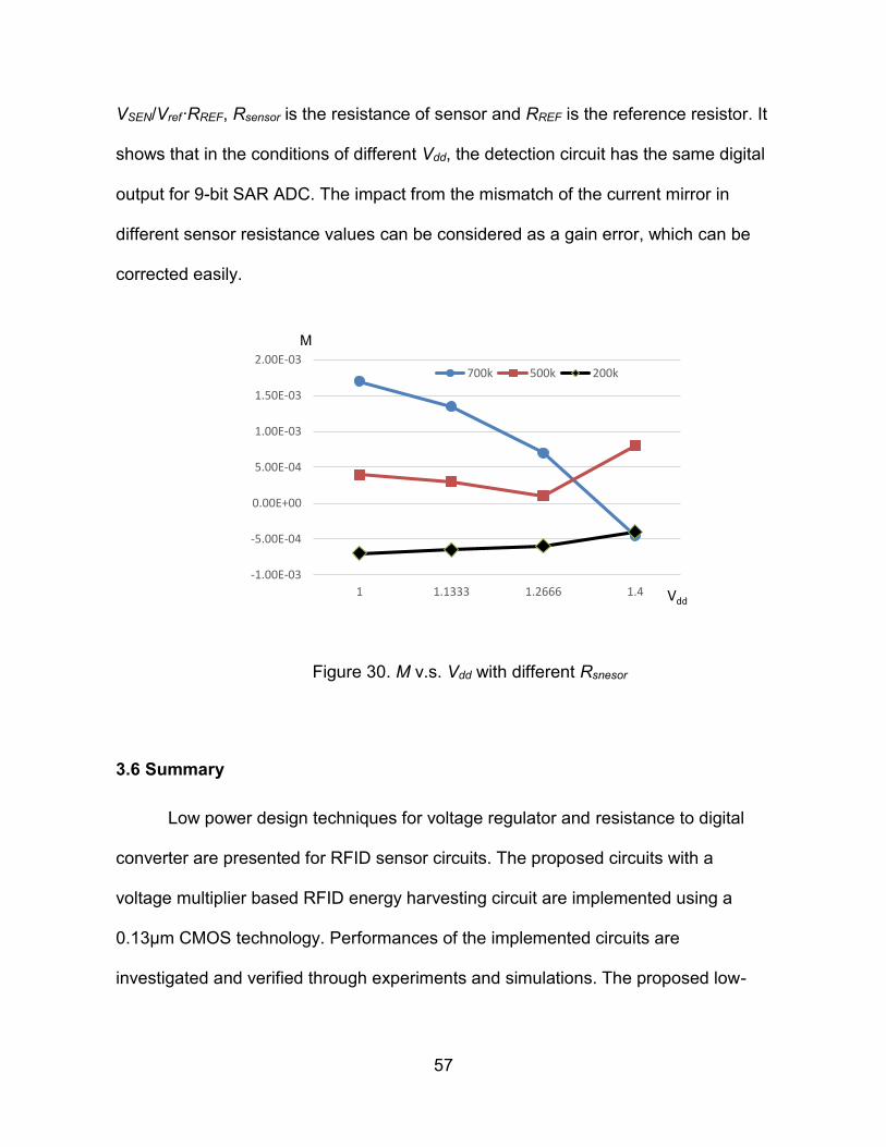
57
VSEN/Vref·RREF, Rsensor is the resistance of sensor and RREF is the reference resistor. It
shows that in the conditions of different Vdd, the detection circuit has the same digital
output for 9-bit SAR ADC. The impact from the mismatch of the current mirror in
different sensor resistance values can be considered as a gain error, which can be
corrected easily.
Figure 30. M v.s. Vdd with different Rsnesor
3.6 Summary
Low power design techniques for voltage regulator and resistance to digital
converter are presented for RFID sensor circuits. The proposed circuits with a
voltage multiplier based RFID energy harvesting circuit are implemented using a
0.13µm CMOS technology. Performances of the implemented circuits are
investigated and verified through experiments and simulations. The proposed low-
-1.00E-03
-5.00E-04
0.00E+00
5.00E-04
1.00E-03
1.50E-03
2.00E-03
1 1.1333 1.2666 1.4
700k 500k 200k
Vdd
M

58
power circuit techniques are not only suitable for the targeted RFID Sol-Gel sensors
but also can be used in the design of other wireless sensors.

59
CHAPTER 4
REDUCTION OF PARASITIC CAPACTIANCE IMPACT IN LOW-POWER SAR
ADC
4.1 Principle of SAR ADC and effects of parasitic capacitance
For the sensor measurement in wireless sensor, single-end SAR ADC is often
used due to the low power requirement and difficulty for the sensor to generate
differential signals. The traditional single-ended SAR ADC usually uses the whole
capacitor array to sample the input voltage. This makes the power consumption
increase and needs a strong buffer to drive the capacitor array. It will consume more
power.
Figure 31. Block diagram of the conventional CS SAR ADC
I Principle of SAR ADC
The single-ended CS SAR ADC normally consists of a charge scaling
capacitor array, a comparator and SAR logic as shown in Figure 31. In the figure,
VCM is the signal ground level, C is the unit capacitance, and CP is the parasitic
capacitance at the top plate of the capacitor array. During the sampling phase,
switch S1 is closed and S2 connects to ADC input Vin. The input voltage is sampled

60
by the entire CS capacitor array. During the conversion phase, switch S1 is open and
S2 connects to Vref. At the beginning of the conversion phase, all the switches labeled
by Dn-1,···D0 are connected to ground terminals. The conversion cycle starts by
switching Dn-1 to Vref. Then, VX, the voltage at the top plates of CS capacitors,
becomes VCM + 0.5·Vref – Vin. If the comparator output is 0, switch Dn-1 remains
connected to Vref; otherwise Dn-1 is switched back to the ground terminal. Similar, the
rest n-1 conversion cycles are performed. At the end of the conversion phase, the
total capacitance connected to Vref is Ceq = Dout·C, where Dout is the ADC digital
output code. Meanwhile, the voltage at the top plate of the CS capacitor array, VX, is
equal to VCM (ignoring the difference less than the VLSB of the ADC). Therefore, we
have:
· · · ·CM in total CM p X ref eq total eqX pV V C V C V V C V C C C (42)
where Ctotal is the total capacitance of the CS capacitor array and its value is 2n·C.
Substituting VX = VCM and Ceq = Dout·C into the above equation, we obtain:
2n inOUT
ref
VD
V (43)
It shows that the ADC output is the correct digital representation of the analog input,
and parasitic capacitance CP does not affect the conversion accuracy of the
conventional SAR ADC, which is one appealing point of the conventional SAR ADC
design.

61
In this circuit, the entire CS capacitor array is used as the sampling
capacitance. The large sampling capacitance (2nC plus the bottom plate parasitic
capacitance) significantly increases the power consumption of the ADC driver circuit.
Assuming that the SAR ADC is driven by an amplifier circuit, for the accuracy
consideration, the nonlinear settling time due to the amplifier slew rate is normally
selected to be smaller than one-eighth of the sampling period and, hence, the power
consumption of the amplifier can be estimated by [31]:
𝑃 = 8 × 𝑓𝑠 × 𝑉𝑚𝑎𝑥 × 𝑉𝐷𝐷 × 𝐶𝑠𝑎𝑚𝑝𝑙𝑒 ×𝑚 (44)
where fS is the ADC sampling frequency, Vmax is the maximum input voltage swing,
CSample is the ADC sampling capacitance and m is a numerical factor related to
amplifier topology with typical values ranging from 2 to 4. Clearly, the energy
dissipation of the circuit driving a conventional CS SAR ADC increases exponentially
with the increase of the ADC resolution.
Figure 32. Diagram of CS SAR ADC with a separate sampling capacitor

62
II Effects of parasitic capacitance in SAR ADC-S2C
To reduce the power consumption of the driver circuits, SAR ADC-S2C (SAR
ADC with separate sampling capacitor) structure is developed [22, 32, 33] and its
block diagram is shown in Figure 32. Normally, Cs is much smaller than the total
capacitance of the CS array and, hence, the power consumption of the ADC driver
circuit is significantly reduced. However, compared to conventional SAR ADC
design, this circuit topology is prone to gain error and reduced ADC input range due
to the parasitic capacitance of the CS capacitor array. In this circuit, the voltage at
the top plate of the CS array, VX, is equal to Vin at the end of the conversion cycles.
Similar to the derivations for the conventional SAR ADC, the expression of VX for the
SAR ADC-S2C structure can be obtained:
2
eq ref
X
total P
OUT ref
n
P
C VV
C C
D C V
C C
(45)
From this relation, the ADC output Dout can be solved as:
2 1
2 1
n in POUT
ref total
n in
ref
V CD
V C
Vh
V
(46)

63
In the above equation, we use h to denote the ratio of Cp over Ctotal. The
above equation shows that a gain error is induced by the existence of CP.
Traditionally, this gain error is corrected by multiplying the ADC output by 1/(1+h).
This method remains effective before the ADC output getting saturated at the
maximum digital code 2n-1. We use VADC-I.R. to denote the lowest ADC input level that
results in the ADC output reaching code 2n-1 for the SAR ADC-S2C design . It is
easy to show:
. .
11
2
1
1
1
n
ADC I R ref
ref
V Vh
Vh
(47)
Essentially, the above equation represents the ADC input range, in which the
gain error can be compensated by multiplication.
Recently, very small unit capacitance values, ranging from several fF to tens
fF, have been used in SAR ADC designs for low-power or high-speed operations [19,
4, 25, 26]. This leads to much large h values and, subsequently, large ADC input
range reduction (compared to Vref) as predicted by Equation 47. Although larger Vref
can be used to address the reduction of the ADC input ranges, high Vref levels will
increase the circuit energy dissipation and may not be practical in circuits with low-
voltage power supply. With the continuous scaling down of device geometric sizes
and the use of new fabrication technologies, the value of h may vary over the time
(e.g. due to device aging or other environmental factors) or change with voltage VX.
In the former scenario, re-calibrations might be needed during the life cycles of the

64
SAR ADC-S2C circuits to keep the effectiveness of the digital gain compensation. In
the latter circumstance, nonlinear error will be induced by CP in SAR ADC-S2C
circuits, which may not be easily compensated. The next section presents an
effective method to compensate the effect of CP. It has minimum hardware overhead;
eliminates the need of calibration process; and is capable of addressing the new
challenges discussed above.
Figure 33. Minimizing the effect of CP in an SAR ADC-S2C circuit
4.2 Proposed circuit technique
The basic idea of the proposed technique is to charge parasitic capacitance
Cp to the ADC input level during the sampling phase. As discussed early, the voltage
at the top plates of the CS capacitors is approximate to Vin at the end of the
conversion process. Therefore, the voltage as well as charge stored in CP does not
change and its effect is minimized. The circuit technique to implement this schematic
is shown in Figure 33. Compared to the original SAR ADC-S2C circuit, three
switches, S3, S4, and S5, are added. During the sampling phase, switches S1, S2 and

65
S3 are closed; S5 connects the bottom plate of the termination capacitor to ADC input
Vin. The ADC input is sampled by CS. Meanwhile, CP is also charged to Vin. Note that
the charge scaling capacitors (2n-1C, 2n-2C…2C, C, C) are not charged since their
both terminals are tied to Vin. During the conversion phase, switches S1, S2, S3 are
open and S4 is closed. Also, S5 switches to node B, which is tied to the ground level.
Thereafter, regular charge scaling operations are performed to generate the ADC
digital outputs.
Similar to the previous discussion, we use Ceq to denote the capacitance tied
to Vref at the end of the conversion phase and, hence, we have:
in P X ref eq X total P eqV C V V C V C C C (48)
Substituting Ceq = Dout·C, Ctotal = 2nC and Vin = VX into the above equation, then we
obtain:
2n in
OUT
ref
VD
V (49)
This clearly indicates that CP does not affect the ADC conversion results in the
proposed circuit. This discussion is based on a constant Cp. It can be shown that the
proposed technique can also effectively minimize the effect of nonlinear parasitic
capacitors (the capacitor value varies with the voltage across the capacitor). Detail
discussions about this case are given in Appendix B.

66
(a) Charge distribution network during
sampling phase
(b) Equivalent circuit of
the charge distribution network during
sampling phase
(c) Charge distribution network during
conversion phase
(d) Equivalent circuit of the charge
distribution network during conversion
phase
Figure 34. Impact of newly added switches in SAR ADC operation
The process of charging Cp to Vin level takes place during the sampling phase.
It does not increase the number of clock cycles per ADC conversion. Also the
proposed technique requires only three additional switches and its hardware
overhead is negligible. Note that switches S3, S4 and S5 connect to the bottom plates
of CS capacitors, which are always tied to a voltage source (Vin, Vref or ground).

67
Hence, channel charge injections associated with S3, S4 and S5 do not affect the
ADC accuracy and these switches can be implemented using simple circuit
structures. Nevertheless, the additional switches in the proposed circuit potentially
affect the ADC speed. Figure 34 (a) shows the network to charge Cp during the
sampling phase. Note that S3 is the newly added switch and Cp2 represent the
parasitic capacitance at the bottom plates of the CS array. The simplified equivalent
circuit of the charging network is shown in Figure 34 (b), where we use r2 and r3 to
represent the on-resistance of switches S2 and S3. rCS is the equivalent on-resistance
of the switches in the CS array. For this type of RC network, if the switch sizes are
optimized such that r2CP = (r3+ rCS)CP2, the circuit performs like a first-order RC
circuit and it tends to result in fast settling time. This is because Ctotal is never
charged and discharged during the entire sampling process. For the conversion
phase, the charging distribution network and its equivalent circuits are shown in
Figure 34 (c) and (d), respectively. In the equivalent circuit, we use CA and CB to
represent the CS capacitors that are connected to Vref and ground, respectively. CAp
and CBp are the parasitic capacitance at the bottom plates of CA and CB. Also, rA and
rB are the equivalent on-resistance of the switches connected to CA and CB; ron_4 is
the on-resistance of switch S4. In the first-order approximation, we ignore CAp, CBp
and CP in the equivalent circuit and it is easy to see the RC time constant of the
resultant circuit is:
4
·( )· A B
A B
A B
C Cr r r
C C
(50)

68
The time constant has the maximum value when CA = CB = 0.5Ctotal. This
occurs during the MSB conversion cycle. Clearly, the additional serial resistance
induced by the switch S4 potentially slows down the charge distribution process and,
hence, the switch on-resistance should be minimized.
In the proposed design, both the top and bottom plates of the capacitor array
are connected to the input voltage during the sampling period. Thus, the equivalent
ADC input capacitance will be CS + CP + CP2. Although the proposed technique
increases the ADC input capacitance compared to the design in Figure 32, it
eliminates the drawbacks of the SAR ADC-S2C circuits, which are discussed in
previous section. Meanwhile, the input capacitance of the proposed design is
normally much smaller than the input capacitance of the conventional SAR ADC
circuit, which includes both the CS array capacitors (2nC) and the parasitic
capacitance (Cp2) at the bottom plates of the CS array (note that the bottom plate of
the CS array in the conventional SAR ADC is also tied to Vin).
It is interesting to see when the proposed design will lose the advantage of
having smaller input capacitance with the continuously scaling down of SAR ADC
unit capacitance. Theoretically, the minimum sampling capacitor CS in the proposed
circuit is limited by the thermal noise of the sampling capacitor network, (KT/CS)1/2,
where K is Boltzmann constant and T is the absolute temperature. If it requires
(KT/CS)1/2 < 1/2VLSB, the minimum sampling capacitor CS,min is:
2 2
,min 2
2 n
S
ref
KTC
V
(51)

69
Practically, the sampling capacitor is selected to be larger than CS,min due to various
concerns and, hence, we assume CS is M times larger than CS,min in this discussion.
For the proposed design, its total input capacitance is CS + Cp + CP2. We use p to
denote the ratio of CP2 over Ctotal. Then, the input capacitance can be rewritten as
CS+(h+p)2nC. Meanwhile, the input capacitance of a conventional SAR ADC is
(1+p)2nC. To keep the advantage of low input capacitance for the proposed design, it
requires:
2 1 2n n
sC h p C p C (52)
Thus, we have:
2
2
12
1
n
ref
KTC M
V h
(53)
The above expression gives the minimum unit capacitance that keeps the
proposed design maintaining its low input capacitance advantage. With the
assumption of M = 10, Vref = V, and h = 10%, the above expression indicates that
the proposed design maintains its low input capacitance advantage until the unit
capacitor is reduced to 0.2 fF for 10-bit ADC and 0.05 fF for 8-bit ADC in future.
Currently, the most aggressively scaled unit capacitors used in the latest SAR ADCs
are in the range of several fF [19] [20] [34] [39]. Due to concerns of matching, yield
and calibration costs, the unit capacitance value will not be scaled into sub fF range

70
soon. As a result, the proposed design will remain as a valid solution for low power
applications.
4.3 Simulation results
I Investigating range of parasitic capacitance CP
In this section, the ranges of the parasitic capacitance in various CS capacitor
array designs are investigated. The study is based on a commercial 0.13µm CMOS
technology. The standard Metal-Insulator-Metal (MIM) capacitors which are available
in most CMOS processes cannot be used to realize the capacitor values in the range
of several fF. Thus, these small unit capacitors used in recent SAR ADCs [19] [20]
[34] [39] are usually constructed using interconnect metal layers. Three types of such
interconnect layer based unit capacitors are developed and their associated parasitic
capacitances are investigated. The first type capacitor, as shown in Figure 35, is
constructed using the third, fourth and fifth metal layers following the structure and
geometric size (5 µm x 5 µm) in [27]. Generally speaking, upper layer metals are
preferred in the construction of such capacitors in order to minimize the parasitic
capacitance to the substrate. For the process used in this study, the minimum size of
the top three metal layers required by the design rules is too large to be used in the
unit capacitor design and, hence, the third, fourth and fifth metal layers are used to
construct the first type unit capacitor. The second type capacitor is similar to the first
type capacitor except that it is implemented by the second, third and fourth metal
layers. Finally, the third type capacitor is developed following the structure and
geometric size (2 µm x 0.4 µm) in [20]. Its capacitor plates are vertical plates

71
constructed by walls of vias, which connect the third, fourth and fifth metal layers as
shown in Figure 36.
a. Cross-section view b. Top view
Figure 35. The first type small unit capacitor used in the study
a. Cross-section view b. Top view
Figure 36. The third type small unit capacitor used in the study
Table 4. Parasitic capacitance ratios of different small unit capacitors
Cap. of M3-M5 sandwich
structure (5 x 5 um)
Cap. of M2-M4 sandwich
structure (5 x 5 um)
Vertical cap. of M3-M5
(2 x 0.4 um)
C 4.78 fF 5.65 fF 0.98 fF
h 12.6% 11.6% 28.3%
p 49.3% 52.7% 69.76%

72
Table 4 lists the unit capacitance C values and parasitic capacitance ratios h
and p obtained from extracted netlists. The extraction is performed using Cadence
Assura tool. It shows that parasitic capacitance at the top plates of the CS capacitor
array will become significant (ranging from 11% to 28% in this study) when small unit
capacitors (fF) are used in the design. If these unit capacitors are used in the SAR
ADC-S2C circuit, the ADC input range will have to be limited within 70%-90% of Vref
in order to effectively compensate the CP-induced gain error in digital domain. Note
that the bottom plate parasitic capacitance is also very significant in the above unit
capacitor structures. This is partially due to the use of thick metal layers in the
construction of the above capacitors and the oxide layers below the thick metal have
relatively large thickness. Also, the fringe capacitance between the vertical vias and
substrate also contributes a significant portion of the total bottom plate parasitic
capacitance.
II Comparison of ADC performance with constant CP
To demonstrate the effectiveness of the proposed technique, the unit
capacitor in Figure 35 is used to implement an 8-bit CS capacitor array for ADC
circuits shown in Figures 31, 32 and 33. The resolution of the ADCs is selected to be
8-bit, mainly for reducing simulation time. Extracted netlist from the entire capacitor
array layout is used in circuit simulations. Since this study aims to demonstrate a
circuit technique to minimize the effect of parasitic capacitance, rather than to
develop a complete ADC circuit, behavior models of comparator and SAR logic are
used with the extracted netlist in simulations. Note that the comparator non-idealities,
such as offset, kick-back, etc., roughly affect all the three ADC circuits equally and

73
techniques to address these effects can be implemented in these three circuits in
similar manners. Thus, the use of comparator behavior mode does not ruin the
validity of the study on how effectively the proposed technique minimizes the
parasitic capacitance induced errors.
The simulations are performed using Cadence Spectre simulator. In the
simulation setup, the circuit power supply and voltage reference are 1.2 V. The ADC
clock frequency is 200 MHz, which leads to a sampling rate of 20 MS/s. To evaluate
the INL and DNL of the ADCs, a ramp signal starting from 0 V and ending at 1.2 V is
used as the ADC input. The slope of the ramp signal is 0.0117 V/µs such that each
ADC output code should occur eight times during the simulation period (102.4 µs) if
the ADC has ideal performance. The ADC outputs are dumped into text files and the
ADC output slopes and gain errors are calculated accordingly. The obtained ADC
output slopes and gain errors for the three ADC topologies are summarized in Table
5. For the convenience of comparisons, two forms of gain errors, in terms of ADC
VLSB and in terms of derivations from the ideal output slopes, are listed in the table.
As expected, the gain of the proposed design as well as that of the conventional
SAR ADC is not affected by parasitic capacitance. However, a gain error of 11% (or
28 VLSB) occurs in the SAR ADC-S2C circuit due to the parasitic capacitance. To be
able to compensate this gain error, the input range of the SAR ADC-S2C circuit has
to be limited within 0.89Vref. The input ranges of the three ADCs are listed in the fifth
row of the table. The six row of the table lists the total sampling capacitance for these
ADCs. Clearly, the conventional SAR ADC has the largest sampling capacitor and

74
the power consumption will also be the largest. The proposed ADC has less
sampling capacitor without induced error from the parasitic capacitance.
Table 5. Comparison of ADC Gain Errors
Conventional
SAR ADC
SAR ADC-S2C
Proposed design
ADC output slope 1 1.112 1
Gain Error
VLSB 0 28 VLSB 0
Deriv. from ideal slope
0 11% 0
Input range (V) 0-1.2 0-1.07 0-1.2
Total load capacitance (pF)
1.83 0.11 0.76
Based on the extracted capacitor values, the energy dissipated by the
sampling capacitors and the charge scaling capacitor arrays of the three ADCs are
estimated using the method in [57]. Figure 37 shows the energy dissipated at
different ADC input levels. The energy dissipation varies with ADC input Vin, because
Vin affects both charge scaling sequences and the voltage across the sampling
capacitance. The energy dissipation of the traditional design reaches its minimum
value when Vin = ½ Vref. This is because VCM is ½Vref in the traditional design and the
voltage across the sampling capacitor (the CS array) is zero when Vin = ½ Vref. The
energy dissipation of the SAR ADC-S2C circuit becomes less independent on ADC
input when Vin > 1.07 V. This is due to that the SAR ADC-S2C circuit has the same
output and goes through the same charge scaling sequence for all the input levels
greater than 1.07 V. Overall, the average energy dissipation of the proposed design

75
is 14.3% less than that of the conventional design. Although the proposed design
consumes about 14.7% more than the SAR ADC-S2C circuit, it overcomes the gain
error and input range reduction associated with the SAR ADC-S2C structure. Note
that the above comparison is only based on the energy dissipated by the sampling
capacitor arrays of the ADCs. If the power consumption of the ADC driver circuits is
also considered, the large sampling capacitance of the traditional design will require
large biasing current in the amplifier that drives the traditional design. According to
the sampling capacitor value listed in Table 4 and Equation 44, the use of the
proposed design can potentially reduce the power consumption of the ADC driver
circuit by 58%, compared to the use of a conventional SAR ADC.
Figure 37. Energy comparisons of the three architectures.

76
Table 6. Transistor sizes of the switches
Switch name S2 S3 S4 S5 D7 D6 D5 D4 D0-D3
Size (W/L) N × (160 nm/120 nm)
60 6 60 1 32 16 8 4 1
Table 7. Comparison of CS array settling time with/without the new switches
Speed Corner
Settling time during MSB charge redistribution Speed
degradation Without new switches
With new switches
TT 2.86 ns 3.80 ns 32.9%
FF 2.20 ns 2.78 ns 26.4%
SS 3.96 ns 5.45 ns 37.6%
Circuit simulations are also performed to investigate the potential speed
degradation caused by the newly added switches during the charge redistribution
phase. Again, the extracted netlist from the 8-bit CS capacitor array layout is used in
simulation. All the switches used in the CS array are implemented using transmission
gates. The transistor sizes of each switch are listed in Table 6. For the simplicity of
the design and potential benefits of canceling channel charge injections, NMOS and
PMOS devices are selected to have the same size in the transmission gate design.
In simulation, we compare the times that are needed for the CS array to settle to
their desired values during the charge redistribution process. As discussed early, the
worst delay occurs during the MSB conversion and, hence, simulation is only
conducted for this type of scenarios. The used simulator is Cadence Spectre. Both
power supply and ADC voltage reference are 1.2 V. The settling accuracy criterion is

77
2 mV, which is about 0.5 VLSB of the 8-bit ADC. Table 7 compares the settling time
during MSB conversion with and without the addition switches at different speed
corners. It shows the additional serial resistance introduced by the new switches can
significantly slow down the charge redistribution process. This problem can be
potentially addressed by using parallel switches, as illustrated in Figure 38, to
implement the same function carried by switch S4. However, this will slightly increase
the area overhead of the ADC implementation.
Figure 38. Parallel switch configuration for minimizing speed degradation
III Comparison of ADC performance with non-linear CP
The parasitic capacitance has a constant value in the above study. Hence, it
only introduces a linear error in the SAR ADC-S2C circuit. However, if the value of CP
is voltage dependent (the case of non-linear parasitic capacitance), CP will also
cause non-linear errors in the SAR ADC-S2C circuit. The proposed technique can
address this non-linear error as well. Although non-linear CP has not gained serious
concerns in current SAR ADC design, it may cause considerable non-linear errors in
future SAR ADC-S2C circuits, as the result of the continuous geometric size scaling
down and the adoption of new fabrication technologies.

78
(a) FFT plot of the Proposed ADC output
(b) FFT plot of the SAR ADC-S2C circuit output
Figure 39. Simulation results of the proposed and SAR ADC-S2C circuits with
variable parasitic capacitance in the CS capacitor array.
To demonstrate that the proposed technique can effectively address the
impact of non-linear CP, we use a behavioral non-linear parasitic capacitor model,
which consists of two serially connected capacitors ca and cb. In the model, ca has a
constant value and the value of cb is governed by the relation cb = c0 + ×VCp, where
c0 and are constant parameters, and VCp is the voltage applied to the parasitic
capacitance. This model is based on the behavior of a metal-insulator-semiconductor
(MIS) capacitor and it uses ca and cb to mimic the behavior of the oxide and depletion
capacitance of the MIS capacitor. This behavioral model is connected in parallel to

79
the CS array unit capacitor to model non-linear CP. For a unit capacitor of 5 fF, we
assign ca and c0 as 1fF and as -0.3. Thus, when the voltage across the unit
capacitor is 0, the parasitic capacitance is 0.5 fF, which is about 10% of the unit
capacitance. The above parameter values are selected to make the parasitic ratio in
the model is inline with the extracted data in Table 4.
An 8-bit CS capacitor array is constructed using the above unit capacitor
along with the non-linear parasitic capacitor model. The capacitor array is used in the
proposed ADC and circuit simulations are conducted to verify that the proposed
technique can address the effect of non-linear CP. In the simulation setup, Vref = 1.2
V; ADC sampling rate is 20 MS/s; and the input signal frequency is 4.0234 MHz in
order to achieve coherent sampling. The FFT plot of the proposed ADC output is
shown in Figure 39 (a). 512 data points are used in the FFT computation and the
obtained SNDR value is 48 dB, which is close to the ideal value. For comparison,
circuit simulations are also performed for an SAR ADC-S2C circuit using the same
CS array. The FFT plot of its output is shown in Figure 39 (b) and the obtained
SNDR is about 38.6 dB (the DC component is excluded from the SNDR
computation). Note that the ADC input swing is 1 V in the above simulations to avoid
ADC output clipping in the SAR ADC-S2C circuit. The finding from the above study
concludes that the proposed technique can effectively address the effect of non-
linear CP
4.4 Concluding remarks
SAR ADC with separate sampling capacitor (SAR ADC-S2C) is an attractive
design choice to implement low-power ADC circuits. However, the parasitic

80
capacitance CP at the charge scaling capacitor arrays of such ADC circuits
introduces gain errors and subsequently reduces the ADC input ranges, which can
be a significant disadvantage in ultra-low voltage ADC design. This section presents
an effective technique to minimize the effect of CP for the SAR ADC-S2C circuit
structure. Simulation results show that the gain error and input range reduction are
effectively removed by the proposed technique for an 8-bit SAR ADC with separate
sampling capacitor. In addition, the proposed technique remains effective even for
the nonlinear parasitic capacitance, which normally causes errors that are difficult to
compensate. The proposed technique does not need calibration processes and
additional clock phases or cycles in ADC conversion operations. The potential speed
degradation caused by the circuit technique is investigated and circuit solution to
address this problem is presented.

81
CHAPTER 5
DIGITAL LDO FOR ULTRA-LOW VOLTAGE OPERATION
5.1 Principle of digital loop LDO regulator
LDO regulator is widely used to provide constant power supply voltage for
other circuits. Because of the power limit in wireless sensors, ultra-low voltage and
ultra-low power LDO is more preferred. In traditional analog LDO, a high gain
operation amplifier (OPAMP) is often needed to generate the stable output voltage.
The OPAMP typically has large power consumption and requires relatively high
power supply. Moreover, a complex loop compensation circuit may be needed in
some applications. These factors make the traditional analog LDO not suitable for
ultra-low power and ultra-low voltage applications. To address this design challenge,
digital LDOs which avoid the use of OPAMP are reported recently [40][41].
DTSP1
DTSN1
PFD
Delay 1 Delay 2 Delay n Delay n Delay 2 Delay 1
Vref
Vo
M1 M2
Id
Ip
Ip
Cp
Rp
M0S1
S2
Figure 40. Digital loop LDO regulator proposed in [41]
VCO2 VCO1

82
Cpout
Delay
DTS
Figure 41. Details of the Delay cell and DTS
Figure 40 is a digital loop LDO regulator proposed in [41]. It consists of an
error amplifier, phase frequency detector (PFD), low pass filter (LPF), a charge pump
circuit and the power FET device. The error amplifier consists of two voltage control
oscillators (VCOs) with the structure of ring oscillator. The frequency of the oscillator
can be calculated as:
𝑓𝑜𝑠𝑐 =1
𝑛𝑇 (54)
where T is the delay of the delay cell and n is the total number of the delay cells. The
circuit of the delay cell is shown in Figure 41. T can be simply derived as:
𝑇 =1
2𝑉𝑑𝑑𝐶𝑐
𝐼0 (55)
where Vdd is the power supply voltage, CC is the capacitance at the output of the
delay cell and Io is the tail current of the delay cell. For the VCO1 in Figure 40, the
vdd
Cc
I0

83
current conducted by M1 is equally distributed to all the delay cells in VCO1. So 𝐼0 =
1
𝑛𝐼𝑀1 and T can be rewritten as:
𝑇 =1
2𝑉𝑑𝑑𝐶𝑐1
𝑛𝐼𝑀1
=𝑛𝑉𝑑𝑑𝐶𝑐
2𝐼𝑀1 (56)
Then the frequency of VCO1 can be derived as:
𝑓𝑜𝑠𝑐,𝑉𝐶𝑂1 =2𝐼𝑀1
𝑛2𝑉𝑑𝑑𝐶𝑐 (57)
In this equation, n, vdd and C0 are parameters selected in the design phase and thus
can be treated as constant during current operation. So the frequency of VCO1 is
determined by the current of M1. Similarly, the frequency of VCO2 can be derived
as:
𝑓𝑜𝑠𝑐,𝑉𝐶𝑂2 =2𝐼𝑀2
𝑛2𝑉𝑑𝑑𝐶𝑐 (58)
Then the difference of the frequencies of the two VCOs is:
𝑓𝑜𝑠𝑐,𝑉𝐶𝑂1 − 𝑓𝑜𝑠𝑐,𝑉𝐶𝑂1 =2𝐼𝑀1
𝑛2𝑉𝑑𝑑𝐶𝑐−
2𝐼𝑀2𝑛2𝑉𝑑𝑑𝐶𝑐
=2
𝑛2𝑉𝑑𝑑𝐶𝑐(𝐼𝑀1 − 𝐼𝑀2)
For the differential input pair M1 and M2, the current can derived as

84
𝐼𝑀1 = 𝑔𝑚1𝑉𝑟𝑒𝑓 (59)
𝐼𝑀2 = 𝑔𝑚2𝑉𝑂 (60)
If gm1 = gm2 = gm, we have:
𝑓𝑜𝑠𝑐,𝑉𝐶𝑂1 − 𝑓𝑜𝑠𝑐,𝑉𝐶𝑂1 =2𝑔𝑚
𝑛2𝑉𝑑𝑑𝐶𝑐(𝑉𝑟𝑒𝑓 − 𝑉𝑜) (61)
The difference of the two VCOs is determined by the differential input voltage. In the
design, DTS cells are used to convert the differential outputs of the VCOs to single-
end signals which are fed to PFD circuits. The signals are also amplified during this
conversion. The PFD is usually implemented by two D-flip-flops. It detects the
difference of the frequencies of the two input square waveforms and generates two
pulse sequences at the output. The width of the output pulse is proportional to the
differences of the frequencies and the phases of the inputs. The charge pump and
the LPF which consists of Cp and Rp are used to convert the pulse from PFD to the
voltage signal which control the power FET device. The voltage of the charge pump
is determined by the two pulses from the PFD, which control S1 and S2 respectively.
When S1 is on, Cp will be charged by Ip, the output voltage of the charge pump will
increase. If S2 is on, Cp will be discharged by Ip, the output voltage of the charge
pump will decrease. Rp is used to improve circuit stability which will be explained in
the stability analysis section. The power FET M0 is used to provide the output load
current. If the gate voltage of the power FET is stable, the drain voltage of M0 which
85
is the output of the LDO regulator will also be stable. The signal waveforms of the
output of the VCOs and S1 in the PFD are shown in Figure 42. In this LDO, OPAMP
circuits are not needed and hence the design challenges associated with low voltage
OPAMP are avoided. The loop is built by digital circuit which can operate under ultra-
low power supply and ultra-low power consumption. The stability compensation is
also simple. Only an extra resistor Rp is added. So the digital LDO regulator is more
suitable for wireless sensor design.
DTSN 1
DTSP 1
S1
Figure 42. Waveform of LDO signals
5.2 System stability
The stability of the system can be analyzed by small signal transfer function.
Figure 43 is the signal flow of the circuit in Figure 40. The first block represents the
error amplifier (EA). KVCO is the gain of the VCO, it is also the gain of EA. The
second block includes PFD, CP and LPF. Ip is the charge pump current; Cp and Rp
are the capacitor and the resistor in the low pass filter. The third block is the power
FET, gm is the transconduction of M0, Rout is the resistance at the output node, Cb is

86
the capacitance at the output node.
Figure 43. Signal flow of the digital LDO in [41]
Figure 44. Pole-zero plot of the LDO system
Then the open loop transfer function can be derived as:
𝑇(𝑠) =𝑉𝑖𝑛
𝑉𝑜𝑢𝑡=
𝐾𝑉𝐶𝑂
𝑠×
𝐼𝑃
2𝜋(𝐼𝑃
𝑠𝐶𝑃+ 𝑅𝑃) × 𝑔
𝑚𝑝× (𝑅𝑜𝑢𝑡||
1
𝑠𝐶𝑏) (62)
𝐾𝑉𝐶𝑂/s
𝐼𝑃2𝜋
(𝐼𝑃𝑠𝐶𝑃
+ 𝑅𝑃) 𝑔𝑚𝑝 × (𝑅𝑜𝑢𝑡||1
𝑠𝐶𝑏) Vref
+
_
Vout
VCO PFD/CP/LPF Power Transistor EA
𝜔𝑝1,2 𝜔𝑝3 𝜔𝑧0

87
It can be re-written as:
𝑇(𝑠) = 𝐴𝑂𝐿(1+𝑠𝐶𝑃𝑅𝑃)
𝑠2(1+𝑠𝐶𝑏𝑅𝑜𝑢𝑡) (63)
𝐴𝑂𝐿 =𝐾𝑣𝑐𝑜𝐼𝑝𝑔𝑚𝑅𝑜𝑢𝑡
2𝜋𝐶𝑃 (64)
where AoL is the open loop dc gain. The transfer function in Equation 63 has three
poles, 𝜔𝑝1,2 = 0, 𝜔𝑝3 =1
𝐶𝑏𝑅𝑜𝑢𝑡, and a zero,𝜔𝑧0 =
1
𝐶𝑃𝑅𝑃. To make the system stable,
we need to push the zero, 𝜔𝑧0, to lower frequency to compensate one pole. That’s
why we need Rp in the low pass filter. To avoid additional poles in low frequency,
𝜔𝑝3 needs to be pushed to higher frequency (higher than the unit gain bandwidth) as
shown in the Figure 44. As long as the zero, 𝜔𝑧0, is low enough and 𝜔𝑝3 is higher
than the bandwidth, the system will be stable. In 𝜔𝑝3 expression, 𝐶𝑏 is mainly from
the parasitic capacitance of the power FET which is usually small compared with Cp;
Rout is determined by the load current, which is small when the load current is large.
So 𝜔𝑝3 is usually at high frequency. By using large Cp and Rp, 𝜔𝑧0 will be low
enough to compensate the pole. But there is a trade-off among the stability, ripple
and bandwidth, which will be explained in next section.
Bandwidth is important for the performance of LDO system. It determines the
response time to the line and the load variation. Large bandwidth benefits fast
response. In the stable condition as Figure 44, the bandwidth can be simply
calculated as:

88
𝐴𝑂𝐿(1+
𝑠
𝜔𝑧0)
𝑠2(1+𝑠
𝜔𝑝3)= 1 (65)
Since 𝜔𝑧0 ≪ 𝜔𝑢𝑛𝑖𝑡_𝑔𝑎𝑖𝑛 ≪ 𝜔𝑝3, it can be simplified as:
𝐴𝑂𝐿(1+
𝜔𝑢𝑛𝑖𝑡_𝑔𝑎𝑖𝑛
𝜔𝑧0)
𝑠2(1+𝜔𝑢𝑛𝑖𝑡_𝑔𝑎𝑖𝑛
𝜔𝑝3)≈ 𝐴𝑂𝐿
𝜔𝑢𝑛𝑖𝑡_𝑔𝑎𝑖𝑛
𝜔𝑧0
(𝜔𝑢𝑛𝑖𝑡_𝑔𝑎𝑖𝑛)2 = 𝐴𝑂𝐿
1
𝜔𝑢𝑛𝑖𝑡_𝑔𝑎𝑖𝑛𝜔𝑧0= 1 (66)
Then we have:
𝜔𝑢𝑛𝑖𝑡_𝑔𝑎𝑖𝑛 =𝐴𝑂𝐿
𝜔𝑧0= 𝐴𝑂𝐿𝐶𝑃𝑅𝑃 =
𝐾𝑣𝑐𝑜𝐼𝑝𝑔𝑚𝑅𝑜𝑢𝑡𝑅𝑃
2𝜋 (67)
So the unit gain bandwidth of the LDO is determined by the gain of the VCO (KVCO),
charge pump current (Ip), Rout, Rp and gm. It’s independent on Cp, so large capacitor
Cp which used to generate the low frequency zero won’t worsen the bandwidth.
Since gm and Rout is decided by the load current, they can’t be increased to improve
the bandwidth. KVCO and Ip are associated with the power consumption. They can
only be increased at the price of increased the power consumption of the LDO, which
is undesirable in low power design. So the most efficient way to increase the
bandwidth is to increase Rp. However, because RP is in the path that IP charge and
discharge CP, a ripple will be generated by Rp, and the amplitude will increase with
Rp. This will increase the noise at the output of LDO.

89
VoRp
Cp
IpFrom PFD
Figure 45. The ripple generated in the LPF
As shown in Figure 45, when S1 is on, the charging current IP will go through
Rp. Thus, a ripple at the gate of M0 will be naturally generated, and it will be
amplified by M0 at output Vo. The amplitude of the ripple at the output can be
calculated as:
𝐴𝑟𝑖𝑝𝑝𝑙𝑒 = 𝐼𝑝𝑅𝑃𝑔𝑚𝑅𝑜𝑢𝑡 (68)
Then the unit gain bandwidth in Equation 67 can be rewritten as:
𝜔𝑢𝑛𝑖𝑡_𝑔𝑎𝑖𝑛 =𝐾𝑣𝑐𝑜𝐴𝑟𝑖𝑝𝑝𝑙𝑒
2𝜋 (69)
S1
S2
M0

90
So we can see that the bandwidth is proportional to the amplitude of the ripple.
Keeping the same current consumption, the bandwidth can only be increased by
increasing Aripple. The ripple is a source of noise which should be minimized in the
LDO. In most of the LDO applications, the amplitude of the ripple is a critical
requirement in the SPECs. So without increasing the power consumption, the
improvement for the bandwidth of the LDO in Figure 40 is very limited.
DTSP
1
PFD1
delay delay delay
Vref
Vo
DTSP
2
DTSP
n
DTSN
1delaydelaydelay
DTSN
2
DTSN
n
PFD2
PFDn
Or gate
M1 M2
Ip
Cp
Rp
M0S1
S2
Figure 46. Proposed digital loop LDO with line and load response improved
VCO1 VCO2

91
5.3 Proposed digital loop LDO regulator
To improve the response time of the line and the load variation, a circuit, as
shown in Figure 46, is proposed in this research. The DTSs (DTSP2,
DTSP3, …,DTSPn, DTSN2, DTSN3,…,DTSNn) are added at the output of each
delay cell in the VCOs. For the output of each pair of delay cells, a PFD is added to
detect the difference of the phases and frequencies. Then the outputs of the PFDs
are sent to the charge pump through an or-gate. In this case, each delay cell will
generate one pulse at one clock cycle. Then there will be totally n pulses in each
clock cycle to the charge pump. n is the number of the delay cells in VCO1 and
VCO2. The signal waveforms of DTSNs for VCO1 and S1 are shown in Figure 47, in
which we take the minimum value, n=3, as an example. In the proposed circuit, each
delay cell generates one pulse, so we have 3 serial pulses in one clock cycle. If
larger n is used in the VCOs, more pulses will show up at S1 in each clock cycle.
The signals of VCO2 have similar behavior. For the reason of conciseness, they are
not shown in Figure 47. In the original design as shown in Figure 42, there is only
one PFD in the LDO and it will only compare the output of one pair delay cell in the
two VCOs. So there is only one pulse at the charge pump in each clock cycle. By
increasing the number of pulse at the charge pump switches, S1 and S2, the
proposed design will improve the response of the line and the load variation in the
LDO.

92
DTSN1
DTSN2
DTSN3
S1
Figure 47. Comparing the signals of the proposed and original work
The proposed design can also be analyzed by small signal analysis. Similar to
the previous analysis, the signal flow of the proposed design is derived as shown in
Figure 48. Because there are n pulses generated in each clock cycle, for the first
stage, it can be modeled as several VCOs with parallel connection. The other blocks
in the circuit model are the same that in Figure 41. Based on this, the transfer
function can be derived as:
𝑇′(𝑠) = 𝑛𝑇(𝑠) = 𝑛𝐴𝑂𝐿(1+𝑠𝐶𝑃𝑅𝑃)
𝑠2(1+𝑠𝐶𝑏𝑅𝑜𝑢𝑡) (70)
where AOL is giving by Equation 64. Then we have:
𝜔𝑢𝑛𝑖𝑡_𝑔𝑎𝑖𝑛 =𝑛𝐾𝑣𝑐𝑜𝐴𝑟𝑖𝑝𝑝𝑙𝑒
2𝜋 (71)

93
So the bandwidth of the proposed LDO becomes n times of the original design.
Because of the increase of the bandwidth, the line and the load response time in the
proposed LDO will be shorter than the one with original structure. It will settle faster
for any variation. Since the calculation of the ripple in the proposed design is the
same to Figure 45, the ripple generated by Rp will be also similar the original work.
For the digital LDO, VCOs and charge pump are two critical blocks which consume
most of the current. In the proposed design, the charge pump current and the tail
current for the VCOs are the same as that in the original design. So the total power
consumption will be similar to the original one. In reality, because of the fast
response of the output variation, the consumed current in the proposed LDO will be a
little less than the one with original structure.
Figure 48. The signal flow of the proposed work
The advantages of the proposed circuit can also be explained by the sampling
system analysis. Comparing to the original work, the frequency of the sampling clock
𝐾𝑉𝐶𝑂/s
𝐼𝑃2𝜋
(𝐼𝑃𝑠𝐶𝑃
+ 𝑅𝑃) 𝑔𝑚𝑝 × (𝑅𝑜𝑢𝑡||1
𝑠𝐶𝑏) Vref
+
_
Vout
PFD/CP/LPF Power Transistor 𝐾𝑉𝐶𝑂/s
𝐾𝑉𝐶𝑂/s
n

94
in the proposed LDO is n times of the original design. Since the maximum bandwidth
of the system is determined by the sampling clock frequency, it's possible to increase
the bandwidth of the system to n times of the original design. This will improve the
response time to the line and the load variation. In the digital LDO, the LDO area is
mainly dominated by the capacitor in LPF, capacitor Cp, and the power FET, M0.
Compared to the original design, the same LPF and power FET are used in the
proposed LDO, and only several small digital cells, DTSs and PFDs, are added. So
the hardware overhead is ignorable.
5.4 Simulation results
To verify the above analysis, two digital loop LDOs with the architectures
shown in Figure 40 and Figure 46 are implemented. The implementation is based on
0.18µm CMOS technology. Both LDOs can operate with the input power supply
voltage as low as 700mV with the output voltage at 600mV. This supply voltage is
significantly lower than that used in analog LDO circuits. 200nA current is used in the
charge pump Ip. The tail current of the error amplifier, Id, is also 200nA. The PFDs
are achieved by D-flip-flops. The total current of the two implemented regulators are
both less than 300nA, which can be further reduced if needed. No off-chip capacitor
is necessary in this design. The sizes of the critical devices used in the design are
listed in Table 8.

95
Table 8. The size of the critical devices in the implemented LDOs
Cp 200pF
Iload 100uA
Power FET M=100,W/L=10um/0.2um
Cload 1pF
Digital circuits W/L=0.5um/0.2um
Vdd 0.7V
Icharge_pump 0.2uA
Itail_EA 0.2uA
Figures 49, 50 and 51 are the simulation results of the two LDOs. The results
of the proposed and conventional design are ploted by solid and dashed lines in the
plots, respectively. Figure 49 shows the startup settling behavior, in which outputs of
the LDOs increase from zero to the target value, 0.6V. The proposed design settles
faster and with a smoother transition than the one with the original structure. It settles
in less than 30µs with ripple less than 15mV. In the simulation, the load current is
100uA and the power supply is 0.7V. Figure 50 shows the load variation response
results, in which the load current increases from 50uA to 100uA and then goes back
to 50uA. The power supply is also 0.7V. In this figure, the response time of the
conventional design is around 1.3ms, the proposed circuit is only 0.5ms. The ripple
at the output caused by the load variation in the proposed design is also less than
that in the conventional circuit. Figure 51 shows the line variation response results.

96
The input power supply increases from 0.7V to 0.72V and then goes back to 0.7V.
The proposed circuit also demonstrate a faster response. Its recovery time is less
than half of the conventional design and the overshot and the undershot are also
less.
Figure 49. Startup of the implemented LDOs
Figure 50. Line variation response of the implemented LDOs
LDO in Figure 46
LDO in Figure 40
Vdd changed from
700mV to 720mV
Vdd changed from
720mV to 700mV

97
Figure 51. Load variation response of the implemented LDOs
Figure 52 and Figure 53 plot the load regulation behavior of the proposed and
conventional digital LDO. The x-axis is the load current, which increases from 50uA
to 1mA, the y-axis is the output voltage. It shows that the proposed design has
similar load regulation as the conventional design. Figure 54 and Figure 55 plot the
ground current of the proposed and the conventional LDO circuits. The x-axis is the
load current, and the y-axis is the ground current in the LDOs. According to the
waveform, the ground current does not increase as the load current increases from
50uA to 1mA. Because of the fast response of the output variation, the current in the
proposed design is a little less than the one in the original structure.
Iload changed from
50uA to 100uA
Iload changed from
100uA to 50uA

98
Figure 52. Load regulation of the proposed LDO
Figure 53. Load regulation with the structure in Figure 40
0.5994
0.5995
0.5996
0.5997
0.5998
0.5999
0.6000
0.6001
0.6002
0.6003
50 185.7 321.4 457.1 592.9 728.6 864.3 1000
0.59500
0.59600
0.59700
0.59800
0.59900
0.60000
0.60100
50 185.7 321.4 457.1 592.9 728.6 864.3 1000
uA
V
uA
V

99
Figure 54. Current consumption of the proposed LDO
Figure 55. Current consumption of the regulator with the structure in Figure 40
5.5 Summary
This chapter presents a novel digital LDO circuit. With the multi-phase
detection technique in the proposed design, the startup settling time and response
time to the line and the load variation are improved without increasing the power
consumption. The proposed digital LDO circuit as well as a conventional digital LDO
258
260
262
264
266
268
270
272
50.0 185.7 321.4 457.1 592.9 728.6 864.3 1000.0
240.0
250.0
260.0
270.0
280.0
290.0
300.0
310.0
50.0 185.7 321.4 457.1 592.9 728.6 864.3 1000.0
uA
nA
uA
nA

100
circuit are implemented using a 0.18µm CMOS technology. Simulation results
validate the advantages of the proposed design.

101
CHAPTER 6
CONCULSIONS AND FUTURE WORK
This dissertation investigates circuit techniques for low power analog circuits
used in wireless sensors. The circuit building blocks that are investigated include
rectifier circuit used in RF energy harvesting, RDC and ADC circuits, energy efficient
as well as low-drop output regulator circuits. These circuits are essential functional
blocks in various wireless sensor circuits. In the design of rectifier circuit used for RF
energy harvesting, an 18-stage rectifier circuit with using zero-threshold NMOSs is
optimized. The critical design trades-off are analyzed and the advantages of using
inductor boosting techniques are studied. The design is implemented using a 0.13µm
CMOS technology and its performance is verified via simulation. In addition, a power
efficient regulator circuit is developed to work with the rectifier circuit in a RFID
sensor application. The regulator starts to provide constant voltage to the sensor
circuits only after enough energy is accumulated in the charge tank, which is fed by
the rectifier circuit. To minimize the power consumption of the regulator circuit, the
proposed design avoids the conventional close-loop circuit configuration, which
requires the use of amplifiers. Instead, it takes advantage of a large gm of the device
that used to provide the output current. Both simulation and hardware measurement
results demonstrate the validity of the proposed design.
For a sol-gel RFID sensor application, a low-power RDC circuit is developed
to work with the aforementioned energy harvesting and regulator circuits. Its low
power advantage is achieved by a novel sampling and conversion scheme, which
reduces the total capacitance used in the CS array of the RDC by half. Also, it allows

102
the input voltage of RDC larger than the reference voltage used in the design. To
accommodate the relatively poor load regulation performance of the regulator, the
CS array of the RDC is charged by a constant current, and subsequently an adaptive
clock cycle is used in the design. Simulation results show the RDC maintains its
designed accuracy at the presence of large power supply voltage variations.
To achieve low power consumption, some applications use SAR ADC
structure with separate sampling capacitor, and also aggressively scale down the
unit capacitor values in the design. This work presented in Chapter 4 investigates the
gain error and input range reduction caused by the parasitic capacitance in such
SAR ADC topology. Subsequently, a novel technique is presented to overcome such
problems. In the proposed technique, the parasitic capacitance is pre-charged to the
final level of the conversion. Without the charge sharing between the capacitor array
and the parasitic capacitance, no error will be induced by the parasitic capacitance.
The traditional SAR ADC, SAR ADC-S2C and the proposed one are implemented
with the 0.13µm CMOS process. Simulation results show that the proposed SAR
ADC and the traditional SAR ADC have no error induced by the parasitic
capacitance. But the power consumption of the proposed SAR ADC is much less
than that in the traditional design. Simulation also demonstrates that the gain error
and the input range reduction of SAR ADC-S2C circuit is significant when small unit
capacitors are used in the design.
Finally, a digital loop LDO is designed for ultra-low voltage applications. The
novelty of the proposed design is to use multi-phase detection to improve the digital
LDO circuit response time. This helps further reduce the power supply voltage of the

103
LDO circuit. This is mainly due to the fact that the charge pump circuit can more
rapidly respond to the frequency change and subsequently reduce its power
consumption in the proposed design. The feedback loop of the LDO is analyzed. It
shows the output ripple and the response time to the line and the load variation can
be reduced by the proposed technique. The proposed LDO circuit and a
conventional digital loop LDO circuit with using phase detection scheme are
implemented using a 0.18µm CMOS technology. Simulation results confirm that the
proposed design significantly improves the circuit response time and reduces output
ripple. It is also noted that the power consumption of the proposed design is slightly
smaller than that of the conventional design, despite of additional phase detectors
being used in the proposed circuit.
Several research directions can be further pushed based on the research
findings presented in this dissertation. First, the SAR ADC circuits can be further
optimized and fabricated. Subsequently, hardware measurement can be performed
to investigate potentially design challenges. Second, additional design optimization
issues are needed for the proposed LDO circuit. For example, the optimization of the
design parameters of the VCO and the charge pump circuits desires a further for the
proposed LDO circuit. Also, a silicon validation for the proposed LDO circuit is need
for an in-depth understanding of the circuit.

104
REFERENCE
[1] L. Q. Zhuang, D. H. Zhang, M. M. Wong, “Wireless Sensor Networks for
Networked Manufacturing Systems, http://www.intechopen.com
/books/export/citation/ReferenceManager/factory-automation/wireless-
sensor-networks-for-networked-manufacturing-systems - 2010-03-01
[2] Levis, P., Patel, N., Culler, D., Shenker, S. “Trickle: A Self Regulating Algorithm
for Code Propagation and Maintenance in Wireless Sensor Networks”, In:
Proceedings of the 1st conference on symposium on Networked Systems Design
and Implementation (NSDI 2004), Berkeley, CA, USA, p. 2. USENIX Association
(2004)
[3] Chenglong Zhang; Haibo Wang, "Reduction of Parasitic Capacitance Impact in
Low-Power SAR ADC," Instrumentation and Measurement, IEEE Transactions on,
vol.61, no.3, pp.587,594, March 2012
[4] Michael Buettner, Ben Greenstein, Richa Prasad, Alanson Sample, Joshua R.
Smith, Daniel Yeager, David Wetherall. “RFID Sensor networks with the intel
WISP” 6th ACM Conference on Embedded Networked Sensor Systems (Sensys
2008).
[5] Toshiyuki Umeda, Hiroshi Yoshida, ”A 950-MHz Rectifier Circuit for
Sensor Network Tags With 10-m Distance”, IEEE JOURNAL OF SOLID-
STATE CIRCUITS, VOL. 41, NO. 1, JANUARY 2006.
[6] Raymond E. Barnett and Jin Liu, “An EEPROM Programming Controller for
Passive UHF RFID Transponders With Gated Clock Regulation Loop
and Current Surge Control”, IEEE JOURNAL OF SOLID-STATE

105
CIRCUITS, VOL. 43, NO. 8, AUGUST 20
[7] Kotani, K., Sasaki, A., Ito, T., ”High-Efficiency Differential-Drive CMOS
Rectifier for UHF RFIDs”, IEEE Journal of Solid-State Circuits, Volume 44,
Issue 11, Nov. 2009.
[8] Ari Juels, ”RFID Security and Privacy: A Research Survey” IEEE Journal on
Selected Areas in Communication (J-SAC) in 2006.
[9] Rob Glidden, Cameron Bockorick, et al., Design of Ultra-Low-Cost UHF
RFID Tags for Supply Chain Applications. IEEE Communications Magazine
August 2004: 140.
[10] U. Karthaus and M. Fischer, ”Fully integrated passive UHF RFID
transponder with 16.7 mu-W minimum RF input power”, IEEE J. Solid-State
Circuits, vol. 38, no. 10, Oct. 2003.
[11] Jari-Pascal Curty, Norbert Joehl, Catherine Dehollain, ”Remotely Pow-
ered Addressable UHF RFID Integrated System”, IEEE JOURNAL OF
SOLID-STATE CIRCUITS, VOL. 40, NO. 11, NOVEMBER 2005
[12] Fatih Kocer and Michael P. Flynn, ”A New Transponder Architecture With
On-Chip ADC for Long-Range Telemetry Applications”, IEEE JOURNAL
OF SOLID-STATE CIRCUITS, VOL. 41, NO. 5, MAY 2006
[13] R. Barnett, S. Lazar, and J. Liu, ”Design of Multistage Rectifiers with
Low-Cost Impedance Matching for Passive RFID Tags”, Proc. IEEE Radio
Frequency Integrated Circuits Symposium, Jun. 2006.
[14] Raymond E. Barnett, Jin Liu and Steve Lazar, ”A RF to DC Voltage
Conversion Model for Multi-Stage Rectifiers in UHF RFID Transponders”,

106
IEEE JOURNAL OF SOLID-STATE CIRCUITS, VOL. 44, NO. 2,
FEBRUARY 2009.
[15] Jun Yi, Wing-Hung Ki and Chi-Ying Tsui, Analysis and Design Strategy of
UHF Micro-Power CMOS Rectifiers for Micro-Sensor and RFID
Applications, IEEE TRANSACTIONS ON CIRCUITS AND SYSTEMS-I:
REGULAR PAPERS, VOL. 54, NO. 1, JANUARY 2007
[16] Balachandran, G.K.; Barnett, R.E., "A 110 nA Voltage Regulator System With
Dynamic Bandwidth Boosting for RFID Systems," Solid-State Circuits, IEEE
Journal of , vol.41, no.9, pp.2019,2028, Sept. 2006
[17] Ferreira, P.M.; Bergeret, E.; Pannier, P., "1.4 V and 300 nA UHF passive RFID
voltage regulator," New Circuits and Systems Conference (NEWCAS), 2012 IEEE
10th International , vol., no., pp.429,432, 17-20 June 2012
[18] Y. K. Cho, Y. D. Jeon, J. W. Nam, and J. K. Kwon, "A 9-bit 80 MS/s Successive
Approximation Register Analog-to-Digital Converter With a Capacitor Reduction
Technique," IEEE Trans. Circuits Syst. II, Exp. Briefs, pp. 1-5, 2010.
[19] C.-C. Liu, S.-J. Chang, G.-Y. Huang, and Y.-Z. Lin, "A 10-bit 50-MS/s SAR ADC
With a Monotonic Capacitor Switching Procedure," IEEE J. Solid-State Circuits,
vol. 45, pp. 731-740, 2010.
[20] P. Harpe, Z. Cui, W. Xiaoyan, G. Dolmans, and H. de Groot, "A 30fJ/conversion-
step 8b 0-to-10MS/s asynchronous SAR ADC in 90nm CMOS," in IEEE ISSCC
Dig. Tech. Papers, 2010, pp. 388-389.

107
[21] H. Kim, Y. Min, Y. Kim, and S. Kim, "A low power consumption 10-bit rail-to-rail
SAR ADC using a C-2C capacitor array," in IEEE Int. Conf. Electron Devices and
Solid-State Circuits, 2008, pp. 1-4.
[22] W.-S. Liew, L. Yao, and Y. Lian, "A moving binary search SAR-ADC for low
power biomedical data acquisition system," in IEEE ASSCC Dig. Tech. Papers,
2008, pp. 646-649.
[23] S.-I. Chang and Y. Euisik, "A low-power area-efficient 8 bit SAR ADC using dual
capacitor arrays for neural microsystems," in IEEE Int. Conf. Engineering in
Medicine and Biology Society, 2009, pp. 1647-1650.
[24] P.-Y. Robert and M. Sawan, "An Ultra-Low-Power Successive-Approximation-
Based ADC for Implantable Sensing Devices," in IEEE Midwest Symp. Circuits
Syst., 2006, pp. 7-11.
[25] M. El Mustapha Ait Yakoub, M. Sawan, and C. Thibeault, "A neuro mimetic ultra-
low power ADC for bio-sensing applications," in Joint IEEE North-East Workshop
on Circuits and Systems and TAISA Conf., 2009, pp. 1-4.
[26] W.-S. Liew, X. Zou, L. Yao, and Y. Lian, "A 1-V 60-µW 16-channel interface
chip for implantable neural recording," in IEEE Custom Integrated Circuits Conf.,
2009, pp. 507-510.
[27] Z. Cao, S. Yan, and Y. Li, "A 32mW 1.25GS/s 6b 2b/step SAR ADC in 0.13um
CMOS," in IEEE ISSCC Dig. Tech. Papers, 2008, pp. 542-634.
[28] J. Craninckx and G. Van der Plas, "A 65fJ/Conversion-Step 0-to-50MS/s 0-to-
0.7mW 9b Charge-Sharing SAR ADC in 90nm Digital CMOS," in IEEE ISSCC Dig.
Tech. Papers, 2007, pp. 246-600.

108
[29] N. Verma and A. P. Chandrakasan, "An Ultra Low Energy 12-bit Rate-Resolution
Scalable SAR ADC for Wireless Sensor Nodes," IEEE J. Solid-State Circuits, vol.
42, pp. 1196-1205, 2007.
[30] J. L. McCreary and P. R. Gray, "All-MOS charge redistribution analog-to-digital
conversion techniques. I," Solid-State Circuits, IEEE Journal of, vol. 10, pp. 371-
379, 1975.
[31] H. Elwan, G. Weinan, R. Sadkowski, and M. Ismail, "A CMOS digitally
programmable class AB OTA circuit," in IEEE 11th Int. Conf. Microelectronics,
2000, pp. 51-54.
[32] C. Zhang, H. Wang, and M. Yen, "Low power analog circuit design for RFID
sensing circuits," in IEEE Int. Conf. RFID, 2010, pp. 16-21.
[33] J. Sauerbrey, D. Schmitt-Landsiedel, and R. Thewes, "A 0.5-V 1-µW successive
approximation ADC,", IEEE J. Solid-State Circuits, vol. 38, pp. 1261-1265, 2003.
[34] M. Azin and P. Mohseni, "A 94-µW 10-b neural recording front-end for an
implantable brain-machine-brain interface device," in IEEE Conf. Biomedical
Circuits and Systems. , 2008, pp. 221-224.
[35] S.-S. Wong, Y. Zhu, C.-H. Chan, U. F. Chio, S.-W. Sin, U. Seng-Pan, and R. P.
Martins, "Parasitic calibration by two-step ratio approaching technique for split
capacitor array SAR ADCs," in IEEE Int. SoC Design Conf., 2009, pp. 333-336.
[36] K. S. Tan, S. Kiriaki, M. de Wit, J. W. Fattaruso, C. Y. Tsay, W. E. Matthews,
and R. K. Hester, "Error correction techniques for high-performance differential
A/D converters,", IEEE J. Solid-State Circuits, vol. 25, pp. 1318-1327, 1990.

109
[37] H.-S. Lee and D. Hodges, "Accuracy considerations in self- calibrating A/D
converters," IEEE Trans. Circuits Syst., vol. 32, pp. 590-597, 1985.
[38] T. Yoshida, M. Akagi, M. Sasaki, and A. Iwata, "A 1V supply successive
approximation ADC with rail-to-rail input voltage range," in IEEE Int. Symp.
Circuits Syst., 2005, pp. 192-195 Vol. 1.
[39] C.-C. Liu, Y.-T. Huang, G.-Y. Huang, S.-J. Chang, C.-M. Huang, and C.-H.
Huang, "A 6-bit 220-MS/s time-interleaving SAR ADC in 0.18um digital CMOS
process," in IEEE Int. Sym. VLSI Design, Automation and Test. , 2009, pp. 215-
218.
[40] Okuma, Y.; Ishida, K.; Ryu, Y.; Xin Zhang; Po-Hung Chen; Watanabe, K.;
Takamiya, M.; Sakurai, T., "0.5-V input digital LDO with 98.7% current efficiency
and 2.7-µA quiescent current in 65nm CMOS," Custom Integrated Circuits
Conference (CICC), 2010 IEEE , vol., no., pp.1,4, 19-22 Sept. 2010
[41] Jiann-Jong Chen; Ming-Shian Lin; Ho-Cheng Lin; Yuh-Shyan Hwang, "Sub-1V
capacitor-free low-power-consumption LDO with digital controlled loop," Circuits
and Systems, 2008. APCCAS 2008. IEEE Asia Pacific Conference on , vol., no.,
pp.526,529, Nov. 30 2008-Dec. 3 2008
[42] Nikitin, P.V.; Rao, K.V.S., "Theory and measurement of backscattering from
RFID tags," Antennas and Propagation Magazine, IEEE , vol.48, no.6,
pp.212,218, Dec. 2006
[43] Curty, J.-P.; Joehl, N.; Krummenacher, F.; Dehollaini, C.; Declercq, M.J., "A
model for μ-power rectifier analysis and design," Circuits and Systems I: Regular
Papers, IEEE Transactions on , vol.52, no.12, pp.2771,2779, Dec. 2005

110
[44] Nhan Tran, Bomson Lee, and Jong-Wook Lee, “Development of Long-Range
UHF-band RFID Tag chip Using Schottky Diodes in Standard CMOS Technology”
2007 IEEE Radio Frequency Integrated Circuits Symposium
[45] Lee, Y.-H.; Peng, S.-Y.; Chiu, C.-C.; Wu, A.C.-H.; Chen, K.-H.; Lin, Y.-H.; Wang,
S.-W.; Tsai, T.-Y.; Huang, C.-C.; Lee, C.-C., "A Low Quiescent Current
Asynchronous Digital-LDO With PLL-Modulated Fast-DVS Power Management in
40 nm SoC for MIPS Performance Improvement," Solid-State Circuits, IEEE
Journal of , vol.48, no.4, pp.1018,1030, April 2013
[46] Bin Nasir, S.; Youngtak Lee; Raychowdhury, A., "Modeling and analysis of
system stability in a distributed power delivery network with embedded digital
linear regulators," Quality Electronic Design (ISQED), 2014 15th International
Symposium on , vol., no., pp.68,75, 3-5 March 2014
[47] Wei-Chung Chen; Su-Yi Ping; Tzu-Chi Huang; Yu-Huei Lee; Ke-Horng Chen;
Chin-Long Wey, "A Switchable Digital–Analog Low-Dropout Regulator for Analog
Dynamic Voltage Scaling Technique," Solid-State Circuits, IEEE Journal of ,
vol.49, no.3, pp.740,750, March 2014
[48] Bakhtiar, AS.; Jalali, M.S.; Mirabbasi, S., "A high-efficiency CMOS rectifier for
low-power RFID tags," RFID, 2010 IEEE International Conference on , vol., no.,
pp.83,88, 14-16 April 2010
[49] Hirairi, K.; Okuma, Y.; Fuketa, H.; Yasufuku, T.; Takamiya, M.; Nomura, M.;
Shinohara, H.; Sakurai, T., "13% Power reduction in 16b integer unit in 40nm
CMOS by adaptive power supply voltage control with parity-based error
prediction and detection (PEPD) and fully integrated digital LDO," Solid-State

111
Circuits Conference Digest of Technical Papers (ISSCC), 2012 IEEE
International , vol., no., pp.486,488, 19-23 Feb. 2012
[50] Shameli, A; Safarian, A; Rofougaran, A; Rofougaran, M.; De Flaviis, F., "Power
Harvester Design for Passive UHF RFID Tag Using a Voltage Boosting
Technique," Microwave Theory and Techniques, IEEE Transactions on , vol.55,
no.6, pp.1089,1097, June 2007
[51] Weis, Stephen A. (2007), RFID (Radio Frequency Identification): Principles and
Applications, MIT CSAIL
[52] Kim, Y.; Li, P., "A 0.38 V near/sub-VT digitally controlled low-dropout regulator
with enhanced power supply noise rejection in 90 nm CMOS process," Circuits,
Devices & Systems, IET , vol.7, no.1, pp.31,41, Jan. 2013
[53] W.-C. Lee and C. Hu, “Modeling gate and substrate currents due to conduction-
and valence-band electron and hole tunneling,” in Proc. IEEE Int. Symp. VLSI
Technol. Dig. Tech. Papers, 2000, pp. 198–199.
[54] K. M. Cao, W.-C. Lee, W. Liu, X. Jin, P. Su, S. K. H. Fung, J. X. An, B. Yu, and
C. Hu, “BSIM4 gate leakage model including source–drain partition,” in IEDM
Tech. Dig., 2000, pp. 815–818.
[55] C.-H. Choi, K.-H. Oh, J.-S. Goo, Z. Yu, and R. W. Dutton, “Direct tunneling
current model for circuit simulation,” in IEDM Tech. Dig., 1999, pp. 735–738.
[56] M. G. Kim, P. K. Hanumolu, U.-K. Moon ¡°A 10MS/s 11b 0.19mm2 Algorithmic
ADC with Improved Clocking,¡± Tech. Digest of VLSI Circuit Symposium,
Honolulu (June 2006).

112
[57] Ginsburg, B.P. Chandrakasan, "An energy-efficient charge recycling approach
for a SAR converter with capacitive DAC", IEEE International Symposium on
Circuits and Systems, 184- 187 Vol. 1, May 2005
[58] Lev, O., M. Tsionsky, L. Rabinovich, V. Glezer, S. Sampath, I. Pankratov, and J.
Gun. "Organically modified sol-gel sensors." Analytical Chemistry 67, no. 1
(1995): 22A-30A.
[59] Shen J., Wang Bo, Liu S., Wang X., Ruan Z., and Li S., “A passive UHF RFID
tag with a dynamic-Vth cancellation rectifier,” Journal of Semiconductors, vol. 34,
no.9, Sep. 2013

APPENDICES

113
APPENDIX A
For a n-bit ADC, assuming the reference voltage linearly decreases during the
operation of the ADC and the digital output is represented as D = Dn-1Dn-2···D2D1D0,
there is:
𝑉𝑎𝑐𝑡𝑢𝑎𝑙 =𝐷𝑛−1
2(𝑉𝑟𝑒𝑓 − 0) +
𝐷𝑛−2
22(𝑉𝑟𝑒𝑓 −
∆𝑉𝑟𝑒𝑓
𝑛) + ⋯+
𝐷1
2𝑛−1(𝑉𝑟𝑒𝑓 −
(𝑛−2)∆𝑉𝑟𝑒𝑓
𝑛) +
𝐷0
2𝑛(𝑉𝑟𝑒𝑓 −
(𝑛−1)∆𝑉𝑟𝑒𝑓
𝑛) = 𝑉𝑖𝑑𝑒𝑎𝑙 − (
𝐷𝑛−2
22+
2𝐷𝑛−3
23+⋯+
(𝑛−2)𝐷1
2𝑛−1+
(𝑛−1)𝐷0
2𝑛) ∙
∆𝑉𝑟𝑒𝑓
𝑛
(72)
where, Vactual is the sampled input voltage, Videal is the voltage calculated from the
digital output, there is
𝑉𝑖𝑑𝑒𝑎𝑙 = (𝐷𝑛−1
2+
𝐷𝑛−2
22+
𝐷𝑛−3
23+⋯+
𝐷1
2𝑛−1+
𝐷0
2𝑛) ∙ ∆𝑉𝑟𝑒𝑓 (73)
Assuming a = ΔV/Vref, the INL could be derived as
𝐼𝑁𝐿 = (1
22+
2
23+⋯+
(𝑛−3)
2𝑛−2+
(𝑛−2)
2𝑛−1+
(𝑛−1)
2𝑛) ∙
∆𝑉𝑟𝑒𝑓
𝑛𝑉𝑟𝑒𝑓
2𝑛
=1
2∑
𝑖
2𝑖∙2𝑛
𝑛∙ 𝑎 =
1
2(2 −𝑛−1
𝑖=1
𝑛+1
2𝑛−1) ∙
2𝑛
𝑛∙ 𝑎 (74)
If n is large enough, then INL is approximately to be

114
𝐼𝑁𝐿 ≈2𝑛∙𝑎
𝑛 (75)
Similarly, the DNL could be also calculated as
𝐷𝑁𝐿 = (𝐷𝑛−2
22− (
2
23+⋯+
(𝑛−3)
2𝑛−2+
(𝑛−2)
2𝑛−1+
(𝑛−1)
2𝑛)) ∙
2𝑛∙𝑎
𝑛= (
1
22−
(𝑛−(𝑛−2))∙2𝑛−3+⋯+(𝑛−3)∙22+(𝑛−2)∙21+(𝑛−1)∙20
2𝑛) ∙
2𝑛∙𝑎
𝑛= (
1
22−
𝑛∙∑ 2𝑖𝑛−3𝑖=0 −
1
2∙∑ (𝑖∙2𝑖)𝑛−2𝑖=1
2𝑛) ∙
2𝑛∙𝑎
𝑛=
(1
22−
2𝑛−1−𝑛∙(2𝑛−3+1)−1
2𝑛) ∙
2𝑛∙𝑎
𝑛≈ (−
1
22+
𝑛
23) ∙
2𝑛∙𝑎
𝑛 (76)
When n is large enough, there is
𝐷𝑁𝐿 ≈ 2𝑛−3 ∙ 𝑎 (77)

115
APPENDIX B
This appendix provides more detail discussions on how the proposed circuit
technique in Chapter 4 minimizes the effect of CP when it is a nonlinear capacitance
(The capacitance value varies with the voltage across the capacitance). For the
proposed circuit shown in Figure 19, during the sampling phase, the voltage across
the parasitic capacitance is Vin. We use CP_0 to denote the capacitance value during
this phase. During the conversion process, the voltage at the top plate of the CS
capacitor array changes and, hence, the value of parasitic capacitance also varies.
Without losing generality, we conduct the discussion for the kth clock cycle of the
conversion process. Also, we use the following notations for the voltage and parasitic
capacitance associated with the kth clock cycle: VXk is the voltage at the top plate of
CS capacitor array; Ckeq
is the total capacitance connected to the Vref; and CP_k is the
parasitic capacitance value corresponding to voltage VXk. According to charge
conservation principle, we can solve VXk as
_ 0
_
k
P in eq refk
X
total P k
C V C VV
C C
(78)
where Ctotal is the total capacitance of the CS capacitor array. Thus the voltage
difference observed by the comparator is

116
_ 0
_
_ 0 _
_1
k
P in eq refk
X in in
total P k
kP P k ineq
ref in
total total
P k
total
C V C VV V V
C C
C C VCV V
C C
C
C
(79)
Note that the denominator term of the above equation is always a positive
number and close to 1 in most design cases. It does not affect the comparator
generating the correct output during conversion (Ignore the offset voltage of the
comparator). The (𝐶𝑒𝑞𝑘
𝐶𝑡𝑜𝑡𝑎𝑙𝑉𝑟𝑒𝑓 − 𝑉𝑖𝑛) term in the numerator represents the desired
comparator input at the kth clock cycle in an ideal ADC circuit (without parasitic). The
(𝐶𝑃_0−𝐶𝑃_𝑘
𝐶𝑡𝑜𝑡𝑎𝑙𝑉𝑖𝑛) represents the effect caused by parasitic capacitance at the top plate of
the CS capacitor array.
If the parasitic capacitance has a constant value, we have CP_0 = CP_k. Thus,
the parasitic capacitance does not affect the accuracy of the ADC conversion. This is
the special case discussed in Section III in Chapter 4. If parasitic capacitance value
varies with the voltage applied to the capacitor, then CP_0 ≠ CP_k. However, if the
magnitude of (𝐶𝑒𝑞𝑘
𝐶𝑡𝑜𝑡𝑎𝑙𝑉𝑟𝑒𝑓 − 𝑉𝑖𝑛) is larger than that of (
𝐶𝑃_0−𝐶𝑃_𝑘
𝐶𝑡𝑜𝑡𝑎𝑙𝑉𝑖𝑛), the polarity of the
comparator input will be determined by the first term of the numerator of the above
equation. Thus the parasitic capacitance will not affect the comparator output as well
as the ADC conversion accuracy. To make the above argument true, we need:
_ 0 _k
P P k ineq
ref in
total total
C C VCV V
C C
(80)

117
Approximately we have VXk =
𝐶𝑒𝑞𝑘
𝐶𝑡𝑜𝑡𝑎𝑙𝑉𝑟𝑒𝑓, and we define ΔVX
k = VXk – Vin, ΔCP
k
= CP_0 – CP_k. The above relation can be rewritten as
k
totalP
k
X in
CC
V V
(81)
Since the maximum Vin value is Vref, a more strict case of the above relation is
k
totalP
k
X ref
CC
V V
(82)
In practical design scenario, the parasitic capacitance variation due to voltage
change from 0 to Vref is much smaller than Ctotal. Thus the above relations are always
satisfied and it concludes that the proposed technique can effectively minimize of the
effect of nonlinear parasitic capacitance in SAR ADC-S2C circuits

118
VITA
Graduate School
Southern Illinois University
Chenglong Zhang
Huazhong University of Sci. & Tech.
Bachelor of Science, Electronic Science and Technology, August 2005
Huazhong University of Sci. & Tech.
Master of Science in Education, Electronic Science and Technology, August 2007
Dissertation Title:
LOW-POWER LOW-VOLTAGE ANALOG CIRCUIT TECHNIQUES FOR
WIRELESS SENSORS
Major Professor: Dr. Haibo Wang
Publications:
Chenglong Zhang; Haibo Wang, "Reduction of Parasitic Capacitance Impact in
Low-Power SAR ADC," Instrumentation and Measurement, IEEE Transactions on ,
vol.61, no.3, pp.587,594, March 2012
Chenglong Zhang; Haibo Wang; Yen, M., "Low power analog circuit design for
2
n
∑ 2 ∑
2
=
=
( )
_
1
i n

119
RFID sensing circuits," RFID, 2010 IEEE International Conference on , vol., no.,
pp.16,21, 14-16 April 2010
Kandala, M.; Sekar, R.; Chenglong Zhang; Haibo Wang, "A low power charge-
redistribution ADC with reduced capacitor array," Quality Electronic Design (ISQED),
2010 11th International Symposium on , vol., no., pp.44,48, 22-24 March 2010