Embed Size (px)
Citation preview

Product
Folder
Sample &Buy
Technical
Documents
Tools &
Software
Support &Community
TMS320F28055, TMS320F28054, TMS320F28053TMS320F28052, TMS320F28051, TMS320F28050
www.ti.com SPRS797B –NOVEMBER 2012–REVISED JULY 2014
TMS320F2805x Piccolo™ Microcontrollers1 Device Overview
1.1 Features1
• High-Efficiency 32-Bit CPU (TMS320C28x) • Peripheral Interrupt Expansion (PIE) Block ThatSupports All Peripheral Interrupts– 60 MHz (16.67-ns Cycle Time)
• Three 32-Bit CPU Timers– 16 x 16 and 32 x 32 MAC Operations• Independent 16-Bit Timer in Each ePWM Module– 16 x 16 Dual MAC• On-Chip Memory– Harvard Bus Architecture
– Flash, SARAM, Message RAM, OTP, CLA Data– Atomic OperationsROM, Boot ROM, Secure ROM Available– Fast Interrupt Response and Processing
• 128-Bit Security Key and Lock– Unified Memory Programming Model– Protects Secure Memory Blocks– Code-Efficient (in C/C++ and Assembly)– Prevents Firmware Reverse Engineering• Programmable Control Law Accelerator (CLA)
• Serial Port Peripherals– 32-Bit Floating-Point Math Accelerator– Three Serial Communications Interface (SCI)– Executes Code Independently of the Main CPU
(Universal Asynchronous Receiver/Transmitter• Dual-Zone Security Module [UART]) Modules• Endianness: Little Endian – One Serial Peripheral Inteface (SPI) Module• Low Device and System Cost: – One Inter-Integrated-Circuit (I2C) Bus
– Single 3.3-V Supply – One Enhanced Controller Area Network (eCAN)– No Power Sequencing Requirement Bus– Integrated Power-on Reset and Brown-out • Enhanced Control Peripherals
Reset – Enhanced Pulse Width Modulator (ePWM)– Low Power – Enhanced Capture (eCAP) Module– No Analog Support Pins – Enhanced Quadrature Encoder Pulse (eQEP)
• Clocking: Module– Two Internal Zero-Pin Oscillators • Analog Peripherals– On-Chip Crystal Oscillator and External Clock – One 12-Bit Analog-to-Digital Converter (ADC)
Input – One On-Chip Temperature Sensor for Oscillator– Watchdog Timer Module Compensation– Missing Clock Detection Circuitry – Up to Seven Comparators With up to Three
• Up to 42 Individually Programmable, Multiplexed Integrated Digital-to-Analog Converters (DACs)General-Purpose Input/Output (GPIO) Pins With – One Buffered Reference DACInput Filtering – Up to Four Programmable Gain Amplifiers
• JTAG Boundary Scan Support (PGAs)– IEEE Standard 1149.1-1990 Standard Test – Up to Four Digital Filters
Access Port and Boundary Scan Architecture • Advanced Emulation Features– Analysis and Breakpoint Functions– Real-Time Debug via Hardware
• 80-Pin PN Low-Profile Quad Flatpack (LQFP)
1
An IMPORTANT NOTICE at the end of this data sheet addresses availability, warranty, changes, use in safety-critical applications,intellectual property matters and other important disclaimers. PRODUCTION DATA.

TMS320F28055, TMS320F28054, TMS320F28053TMS320F28052, TMS320F28051, TMS320F28050SPRS797B –NOVEMBER 2012–REVISED JULY 2014 www.ti.com
1.2 Applications• White Goods • AC/DC Inverters• Solar Microinverters and Converters • General Motor Control• Sewing and Textile Machines
1.3 DescriptionThe F2805x Piccolo™ family of microcontrollers (MCUs) provides the power of the C28x core and CLAcoupled with highly integrated control peripherals in low pin-count devices. This family is code-compatiblewith previous C28x-based code, and also provides a high level of analog integration.
An internal voltage regulator allows for single-rail operation. Analog comparators with internal 6-bitreferences have been added and can be routed directly to control the PWM outputs. The ADC convertsfrom 0 to 3.3-V fixed full-scale range and supports ratio-metric VREFHI/VREFLO references. The ADCinterface has been optimized for low overhead and latency.
The Analog Front End (AFE) contains up to seven comparators with up to three integrated DACs, oneVREFOUT-buffered DAC, up to four PGAs, and up to four digital filters. The PGAs can amplify the inputsignal in three discrete gain modes. The actual number of AFE peripherals will depend upon theTMS320F2805x device number. See Section 8 for more details.
Device Information (1)
PART NUMBER PACKAGE BODY SIZETMS320F28055PN LQFP (80) 12.0 mm x 12.0 mmTMS320F28054PN LQFP (80) 12.0 mm x 12.0 mmTMS320F28053PN LQFP (80) 12.0 mm x 12.0 mmTMS320F28052PN LQFP (80) 12.0 mm x 12.0 mmTMS320F28051PN LQFP (80) 12.0 mm x 12.0 mm
(1) For more information on these devices, see Section 8, Mechanical Packaging and OrderableInformation.
2 Device Overview Copyright © 2012–2014, Texas Instruments IncorporatedSubmit Documentation Feedback
Product Folder Links: TMS320F28055 TMS320F28054 TMS320F28053 TMS320F28052 TMS320F28051TMS320F28050
M0
SARAM 1Kx16
(0-wait)
16-bit Peripheral Bus
M1
SARAM 1Kx16
(0-wait)
SCI-A,B C
(4L FIFO)SCI- , SCI-
SP
ISIM
OA
SP
ISO
MIA
SP
ICL
KA
SP
IST
EA
ePWM1–ePWM7SPI-A
(4L FIFO)
I2C-A
(4L FIFO)
32-BitPeripheral Bus
GPIO MUX
C28x CPU(60 MHz)
PIE(up to 96 interrupts)
CPU Timer 0
CPU Timer 1
CPU Timer 2
TRST
TCK
TDITMS
TDO
OSC1,
OSC2,
Ext,
PLL,
LPM,
WD
X2
32-bit Peripheral Bus(CLA-accessible)
EP
WM
xA
EP
WM
xB
SD
Ax
SC
Lx
SC
IRX
Dx
GPIOMux
LPM Wakeup
CLA +Message RAMs
ADC0-waitResultRegs
Boot ROM
12Kx16
(0-wait)Non-Secure
L0 SARAM (2Kx16)(0-wait, Secure)CLA Data RAM2
COMP+
DigitalFilterCOMPAn
COMPBn
32-b
it P
eri
ph
era
l B
us
(CL
A-a
ccessib
le)
eCAN-A
(32-mbox)eCAP
EC
AP
x
CA
NT
Xx
CA
NR
Xx
eQEP
EQ
EP
xA
EQ
EP
xB
EQ
EP
xI
EQ
EP
xS
SC
ITX
Dx
X1
GPIO
MUX
Program-mableGainAmps
VREGPOR/BOR
Mem
ory
Bu
s
Memory Bus
TZ
x
Secure ROM(A)
2Kx16
(0-wait)Secure
L1 DPSARAM (1Kx16)(0-wait, Secure)CLA Data RAM0
L2 DPSARAM (1Kx16)(0-wait, Secure)CLA Data RAM1
L3 DPSARAM (4Kx16)(0-wait, Secure)
CLA Program RAM
CLA Data ROM(4Kx16)
CTRIPnOUT
ADC3.75
MSPS
32-bit Peripheral Bus(CLA-accessible)
CL
AB
us
XRS
GPIOMux
XCLKIN
3 External Interrupts
Memory Bus
EP
WM
SY
NC
I
EP
WM
SY
NC
O
PSWD
Dual-Zone
SecurityModule
+ECSL
OTP/Flash Wrapper
Z1/Z2 User OTPSecure
PUMP
FLASH
28055, 28054: 64K x 16, 10 Sectors
28053, 28052, 28051: 32K x 16, 5 Sectors
28050: 16K x 16, 3 Sectors
Secure
TMS320F28055, TMS320F28054, TMS320F28053TMS320F28052, TMS320F28051, TMS320F28050
www.ti.com SPRS797B –NOVEMBER 2012–REVISED JULY 2014
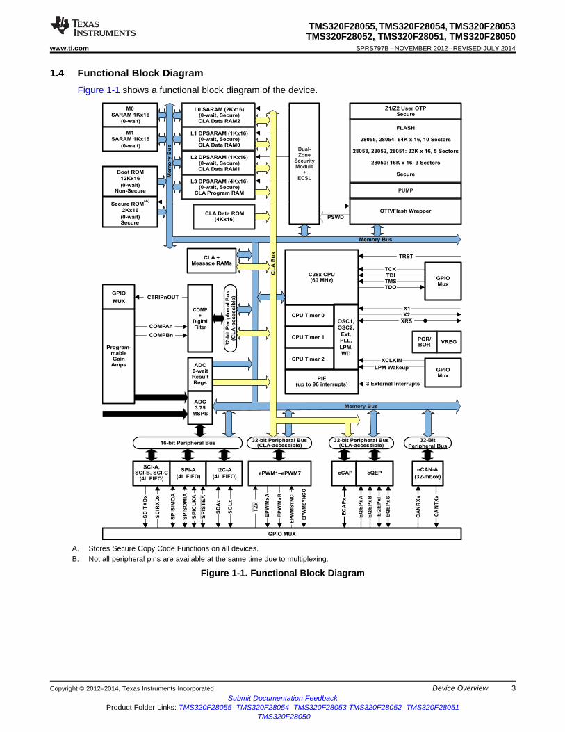
1.4 Functional Block DiagramFigure 1-1 shows a functional block diagram of the device.
A. Stores Secure Copy Code Functions on all devices.B. Not all peripheral pins are available at the same time due to multiplexing.
Figure 1-1. Functional Block Diagram
Copyright © 2012–2014, Texas Instruments Incorporated Device Overview 3Submit Documentation Feedback
Product Folder Links: TMS320F28055 TMS320F28054 TMS320F28053 TMS320F28052 TMS320F28051TMS320F28050

TMS320F28055, TMS320F28054, TMS320F28053TMS320F28052, TMS320F28051, TMS320F28050SPRS797B –NOVEMBER 2012–REVISED JULY 2014 www.ti.com
Table of Contents1 Device Overview ......................................... 1 5.12 Clock Specifications ................................. 31
1.1 Features .............................................. 1 5.13 Flash Timing ........................................ 341.2 Applications........................................... 2 6 Detailed Description ................................... 361.3 Description............................................ 2 6.1 Overview ............................................ 361.4 Functional Block Diagram ............................ 3 6.2 Memory Maps ...................................... 47
2 Revision History ......................................... 5 6.3 Register Map ........................................ 543 Device Comparison ..................................... 9 6.4 Device Emulation Registers......................... 564 Terminal Configuration and Functions ............ 11 6.5 VREG, BOR, POR .................................. 58
4.1 Signal Descriptions.................................. 12 6.6 System Control ...................................... 605 Specifications ........................................... 19 6.7 Low-power Modes Block ............................ 68
5.1 Absolute Maximum Ratings ........................ 19 6.8 Interrupts ............................................ 695.2 Handling Ratings ................................... 19 6.9 Peripherals .......................................... 745.3 Recommended Operating Conditions............... 20 7 Device and Documentation Support .............. 1405.4 Electrical Characteristics ............................ 20 7.1 Device Support..................................... 1405.5 Thermal Resistance Characteristics for PN 7.2 Documentation Support............................ 143
Package ............................................. 21 7.3 Related Links ...................................... 1445.6 Thermal Design Considerations .................... 21 7.4 Community Resources............................. 1445.7 Emulator Connection Without Signal Buffering for 7.5 Trademarks ........................................ 144
the MCU............................................. 227.6 Electrostatic Discharge Caution ................... 144
5.8 Current Consumption................................ 237.7 Glossary............................................ 144
5.9 Parameter Information .............................. 278 Mechanical Packaging and Orderable
5.10 Test Load Circuit ................................... 27 Information ............................................. 1455.11 Power Sequencing .................................. 28 8.1 Packaging Information ............................. 145
4 Table of Contents Copyright © 2012–2014, Texas Instruments IncorporatedSubmit Documentation Feedback
Product Folder Links: TMS320F28055 TMS320F28054 TMS320F28053 TMS320F28052 TMS320F28051TMS320F28050
TMS320F28055, TMS320F28054, TMS320F28053TMS320F28052, TMS320F28051, TMS320F28050
www.ti.com SPRS797B –NOVEMBER 2012–REVISED JULY 2014
2 Revision HistoryNOTE: Page numbers for previous revisions may differ from page numbers in the current version.
This data sheet revision history highlights the technical changes made to the SPRS797A device-specificdata sheet to make it an SPRS797B revision.
Scope: Added InstaSPIN-MOTION™ devices TMS320F28054M and TMS320F28052M. See Table 3-1.Added InstaSPIN-FOC™ devices TMS320F28054F and TMS320F28052F. See Table 3-1.TMS320F2805x devices are now available in the Q temperature range (–40°C to 125°C, Q100 qualification forautomotive applications). See Table 3-1.Added Section 7.3, Related Links, which provides quick access to available resources.Restructured document.See the following table.
LOCATION ADDITIONS, DELETIONS, AND MODIFICATIONSGlobal • Restructured document
• TMS320F2805x devices are now available in the Q temperature range (–40°C to 125°C, Q100qualification for automotive applications). See Table 3-1.
• Removed Reliability Data for TMS320LF24xx and TMS320F28xx Devices Application Report(SPRA963)
Section 1 Changed section title from "TMS320F2805x (Piccolo) Microcontrollers" to "Device Overview"Section 1.1 Features:
• Clocking:– Removed "Dynamic Phase-Locked Loop (PLL) Ratio Changes Supported"
Section 1.2 Added "Applications" sectionSection 1.3 Description:
• Added "Device Information" tableSection 3 Added "Device Comparison" sectionTable 3-1 Changed title from "TMS320F2805x Hardware Features" to "Device Comparison"Table 3-1 Device Comparison:
• Added InstaSPIN-MOTION devices TMS320F28054M and TMS320F28052M• Added InstaSPIN-FOC devices TMS320F28054F and TMS320F28052F• Added "Q: –40ºC to 125ºC" to Temperature options• Added footnote with reference to a list of InstaSPIN™ Technical Reference Manuals (Section 7.2)• Added footnote about Q100 qualification
Section 4 Changed section title from "Device Pins" to "Terminal Configuration and Functions"Section 4.1 Changed section title from "Terminal Functions" (Section 3.2 in SPRS797A) to "Signal Descriptions".Table 4-1 Changed table title from "Terminal Functions" to "Signal Descriptions"Table 4-1 Signal Descriptions:
• Pin 8 (XRS): Updated "I/O/Z" column and DESCRIPTION• Pins 6, 54, 73 (VDD): Updated DESCRIPTION• Pin 42 (GPIO28): Changed SDAA from "I/OD" to "I/OC"• Pin 41 (GPIO29): Changed SCLA from "I/OD" to "I/OC"• Pin 2 (GPIO32): Changed SDAA from "I/OD" to "I/OC"• Pin 3 (GPIO33): Changed SCLA from "I/OD" to "I/OC"• Added definition of "OC" to footnote
Section 5 Changed title from "Device Operating Conditions" (Section 4 in SPRS797A) to "Specifications"Section 5.1 Absolute Maximum Ratings:
• Moved Storage temperature range, Tstg, to the new "Handling Ratings" sectionSection 5.2 Added "Handling Ratings" sectionSection 5.3 Recommended Operating Conditions:
• Added Junction temperature, TJ, for Q versionSection 5.5 Changed title from "Thermal Model 80-Pin PN Results" (Table 9-1 in SPRS797A) to "Thermal Resistance
Characteristics for PN Package"
Copyright © 2012–2014, Texas Instruments Incorporated Revision History 5Submit Documentation Feedback
Product Folder Links: TMS320F28055 TMS320F28054 TMS320F28053 TMS320F28052 TMS320F28051TMS320F28050

TMS320F28055, TMS320F28054, TMS320F28053TMS320F28052, TMS320F28051, TMS320F28050SPRS797B –NOVEMBER 2012–REVISED JULY 2014 www.ti.com
LOCATION ADDITIONS, DELETIONS, AND MODIFICATIONSSection 5.5 Thermal Resistance Characteristics for PN Package:
• Reformatted table• Added footnotes
Table 5-7 Internal Zero-Pin Oscillator (INTOSC1, INTOSC2) Characteristics:• Accuracy using oscillator compensation:
– Removed "TBD" from MAX columnTable 5-13 Added "Flash/OTP Endurance for Q Temperature Material" tableTable 5-14 Flash Parameters at 60-MHz SYSCLKOUT:
• Updated "Typical parameters as seen at room temperature ..." footnoteTable 6-13 Device Emulation Registers:
• Added PARTID for 28054M, 28054F, 28052M, and 28052F devicesFigure 6-5 Updated "VREG + POR + BOR + Reset Signal Connectivity" figureFigure 6-11 Updated "CPU-watchdog Module" figureSection 6.9 Changed title from "Peripheral Information and Timings" (Section 6 in SPRS797A) to "Peripherals"Table 6-44 PGA Gain Stage: DC Accuracy Across Gain Settings:
• Changed "COMPENSATED GAIN-ERROR DRIFT ACROSS TEMPERATURE AND SUPPLYVARIATIONS" column heading to "COMPENSATED GAIN-ERROR ACROSS TEMPERATURE ANDSUPPLY VARIATIONS"
Table 6-45 Electrical Characteristics of the Comparator/DAC:• Removed "Input Offset"• Removed "Input Hysteresis"
6 Revision History Copyright © 2012–2014, Texas Instruments IncorporatedSubmit Documentation Feedback
Product Folder Links: TMS320F28055 TMS320F28054 TMS320F28053 TMS320F28052 TMS320F28051TMS320F28050

TMS320F28055, TMS320F28054, TMS320F28053TMS320F28052, TMS320F28051, TMS320F28050
www.ti.com SPRS797B –NOVEMBER 2012–REVISED JULY 2014
LOCATION ADDITIONS, DELETIONS, AND MODIFICATIONSTable 6-68 GPIOA MUX:
• Updated PERIPHERAL SELECTION 1 for the following GPAMUX1 REGISTER BITS:– 25-24: Changed "TZ1 (I)" to "TZ1 (I)/CTRIPM1OUT (O)"– 29-28: Changed "TZ3 (I)" to "TZ3 (I)/CTRIPPFCOUT (O)"– 31-30: Changed "TZ1 (I)" to "TZ1 (I)/CTRIPM1OUT (O)"
• Updated PERIPHERAL SELECTION 2 for the following GPAMUX1 REGISTER BITS:– 19-18: Changed "Reserved" to "SCITXDB (O)"– 23-22: Changed "Reserved" to "SCIRXDB (I)"– 29-28: Changed "Reserved" to "SCITXDB (O)"– 31-30: Changed "Reserved" to "SCIRXDB (I)"
• Updated PERIPHERAL SELECTION 3 for the following GPAMUX1 REGISTER BITS:– 3-2: Changed "COMP1OUT (O)" to "CTRIPM1OUT (O)"– 7-6: Changed "COMP2OUT (O)" to "Reserved"
• Updated PERIPHERAL SELECTION 2 for the following GPAMUX2 REGISTER BITS:– 1-0: Changed "Reserved" to "EQEP1S (I/O)"– 3-2: Changed "Reserved" to "EQEP1I (I/O)"– 5-4: Changed "Reserved" to "SCITXDB (O)"– 7-6: Changed "Reserved" to "SCIRXDB (I)"– 9-8: Changed "Reserved" to "EPWM7A (O)"– 11-10: Changed "Reserved" to "EPWM7B (O)"– 17-16: Changed "Reserved" to "EPWM7A (O)"– 21-20: Changed "Reserved" to "SCIRXDC (O)"– 23-22: Changed "Reserved" to "SCITXDC (O)"– 25-24: Changed "SDAA (I/OD)" to "SDAA (I/OC)"– 27-26: Changed "SCLA (I/OD)" to "SCLA (I/OC)"– 29-28: Changed "Reserved" to "SCIRXDB (I)"– 31-30: Changed "Reserved" to "SCITXDB (I)"
• Updated PERIPHERAL SELECTION 3 for the following GPAMUX2 REGISTER BITS:– 3-2: Changed "TZ3 (I)" to "TZ3 (I)/CTRIPPFCOUT (O)"– 9-8: Changed "COMP1OUT (O)" to "CTRIPM1OUT (O)"– 11-10: Changed "COMP2OUT (O)" to "Reserved"– 13-12: Changed "Reserved" to "SCITXDB (O)"– 15-14: Changed "Reserved" to "SCIRXDB (I)"– 27-26: Changed "TZ3 (I)" to "TZ3 (I)/CTRIPPFCOUT (O)"– 29-28: Changed "Reserved" to "EPWM7A (O)"– 31-30: Changed "Reserved" to "EPWM7B (O)"
• Added definition of "OC" to footnoteTable 6-69 GPIOB MUX:
• Updated PERIPHERAL SELECTION 1 for the following GPBMUX1 REGISTER BITS:– 1-0: Changed "SDAA (I/OD)" to "SDAA (I/OC)"– 3-2: Changed "SCLA (I/OD)" to "SCLA (I/OC)"– 5-4: Changed "COMP2OUT (O)" to "Reserved"– 17-16: Changed "Reserved" to "EPWM7A (O)"– 19-18: Changed "EPWM7B (O)" to "Reserved"
• Updated PERIPHERAL SELECTION 2 for the following GPBMUX1 REGISTER BITS:– 15-14: Changed "Reserved" to "SCIRXDC (I)"
• Updated PERIPHERAL SELECTION 3 for the following GPBMUX1 REGISTER BITS:– 1-0: Changed "ADCSOCAO (O)" to "EQEP1S (I/O)"– 3-2: Changed "ADCSOCBO (O)" to "EQEP1I (I/O)"– 5-4: Changed "COMP3OUT (O)" to "CTRIPPFCOUT (O)"– 15-14: Changed "Reserved" to "CTRIPPFCOUT (O)"– 21-20: Changed "COMP1OUT (O)" to "CTRIPM1OUT (O)"
• Added definition of "OC" to footnoteSection 7 Device and Documentation Support:
• Added Section 7.3, Related Links• Added "Trademarks" section• Added "Electrostatic Discharge Caution" section• Added "Glossary" section
Copyright © 2012–2014, Texas Instruments Incorporated Revision History 7Submit Documentation Feedback
Product Folder Links: TMS320F28055 TMS320F28054 TMS320F28053 TMS320F28052 TMS320F28051TMS320F28050

TMS320F28055, TMS320F28054, TMS320F28053TMS320F28052, TMS320F28051, TMS320F28050SPRS797B –NOVEMBER 2012–REVISED JULY 2014 www.ti.com
LOCATION ADDITIONS, DELETIONS, AND MODIFICATIONSFigure 7-1 Device Nomenclature:
• Added "Q = −40°C to 125°C (Q refers to Q100 qualification for automotive applications.)" underTEMPERATURE RANGE
Section 7.2 Documentation Support:• Added InstaSPIN Technical Reference Manuals section:
– Added InstaSPIN-FOC™ and InstaSPIN-MOTION™ User's Guide (SPRUHJ1)– Added TMS320F28054F, TMS320F28052F InstaSPIN-FOC™ Software Technical Reference
Manual (SPRUHW0)– Added TMS320F28054M, TMS320F28052M InstaSPIN-MOTION™ Software Technical Reference
Manual (SPRUHW1)• Added Application Reports section:
– Added Semiconductor Packing Methodology Application Report (SZZA021)
8 Revision History Copyright © 2012–2014, Texas Instruments IncorporatedSubmit Documentation Feedback
Product Folder Links: TMS320F28055 TMS320F28054 TMS320F28053 TMS320F28052 TMS320F28051TMS320F28050

TMS320F28055, TMS320F28054, TMS320F28053TMS320F28052, TMS320F28051, TMS320F28050
www.ti.com SPRS797B –NOVEMBER 2012–REVISED JULY 2014
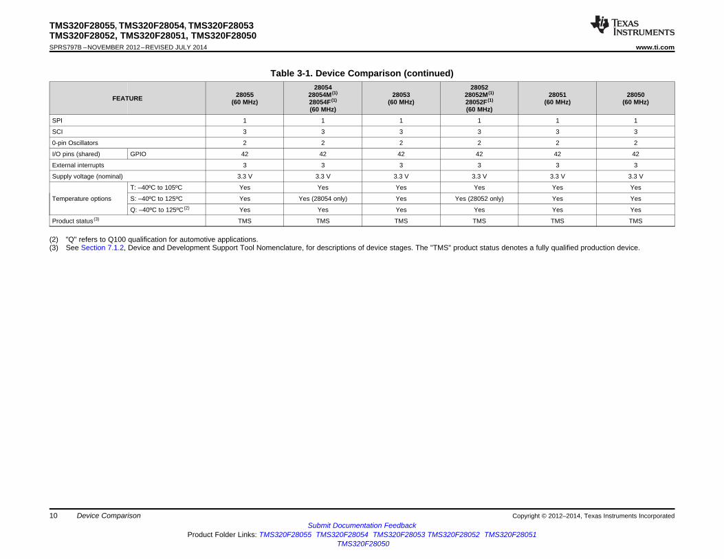
3 Device Comparison
Table 3-1 lists the features of the TMS320F2805x devices.
Table 3-1. Device Comparison28054 28052
28055 28054M (1) 28053 28052M (1) 28051 28050FEATURE (60 MHz) 28054F (1) (60 MHz) 28052F (1) (60 MHz) (60 MHz)(60 MHz) (60 MHz)
80-Pin PN 80-Pin PN 80-Pin PN 80-Pin PN 80-Pin PN 80-Pin PNPackage Type LQFP LQFP LQFP LQFP LQFP LQFP
Instruction cycle 16.67 ns 16.67 ns 16.67 ns 16.67 ns 16.67 ns 16.67 ns
CLA Yes No Yes No No No
On-chip flash (16-bit word) 64K 64K 32K 32K 32K 16K
10K (28054) 10K (28052)On-chip SARAM (16-bit word) 10K 8K (28054M) 10K 8K (28052M) 8K 6K
8K (28054F) 8K (28052F)
Dual-zone security for on-chip Flash, SARAM, OTP, Yes Yes Yes Yes Yes Yesand Secure ROM blocks
Boot ROM (12K x 16) Yes Yes Yes Yes Yes Yes
One-time programmable (OTP) ROM 1K 1K 1K 1K 1K 1K(16-bit word)
ePWM channels 14 14 14 14 14 14
eCAP inputs 1 1 1 1 1 1
eQEP modules 1 1 1 1 1 1
Watchdog timer Yes Yes Yes Yes Yes Yes
MSPS 3.75 3.75 3.75 3.75 2 2
Conversion Time 267 ns 267 ns 267 ns 267 ns 500 ns 500 ns
Channels 16 16 16 16 16 1612-Bit ADCTemperature Sensor Yes Yes Yes Yes Yes Yes
Dual Yes Yes Yes Yes Yes YesSample-and-Hold
PGA (Gains = ~3, ~6, ~11) 4 4 4 4 4 3
Fixed Gain Amplifier (Gain = ~3) 3 3 3 3 3 4
Comparators 7 7 7 7 7 6
Internal Comparator Reference DACs 3 3 3 3 3 2
Buffered Reference DAC 1 1 1 1 1 1
32-Bit CPU timers 3 3 3 3 3 3
1 1 1 1 1 1I2C
eCAN 1 1 1 1 1 1
(1) TMS320F2805xM devices are InstaSPIN-MOTION-enabled MCUs. TMS320F2805xF devices are InstaSPIN-FOC-enabled MCUs. For more information, see Section 7.2 for a list ofInstaSPIN Technical Reference Manuals.
Copyright © 2012–2014, Texas Instruments Incorporated Device Comparison 9Submit Documentation Feedback
Product Folder Links: TMS320F28055 TMS320F28054 TMS320F28053 TMS320F28052 TMS320F28051TMS320F28050
TMS320F28055, TMS320F28054, TMS320F28053TMS320F28052, TMS320F28051, TMS320F28050SPRS797B –NOVEMBER 2012–REVISED JULY 2014 www.ti.com
Table 3-1. Device Comparison (continued)28054 28052
28055 28054M (1) 28053 28052M (1) 28051 28050FEATURE (60 MHz) 28054F (1) (60 MHz) 28052F (1) (60 MHz) (60 MHz)(60 MHz) (60 MHz)
SPI 1 1 1 1 1 1
SCI 3 3 3 3 3 3
0-pin Oscillators 2 2 2 2 2 2
I/O pins (shared) GPIO 42 42 42 42 42 42
External interrupts 3 3 3 3 3 3
Supply voltage (nominal) 3.3 V 3.3 V 3.3 V 3.3 V 3.3 V 3.3 V
T: –40ºC to 105ºC Yes Yes Yes Yes Yes Yes
Temperature options S: –40ºC to 125ºC Yes Yes (28054 only) Yes Yes (28052 only) Yes Yes
Q: –40ºC to 125ºC (2) Yes Yes Yes Yes Yes Yes
Product status (3) TMS TMS TMS TMS TMS TMS
(2) "Q" refers to Q100 qualification for automotive applications.(3) See Section 7.1.2, Device and Development Support Tool Nomenclature, for descriptions of device stages. The "TMS" product status denotes a fully qualified production device.
10 Device Comparison Copyright © 2012–2014, Texas Instruments IncorporatedSubmit Documentation Feedback
Product Folder Links: TMS320F28055 TMS320F28054 TMS320F28053 TMS320F28052 TMS320F28051TMS320F28050
20
1 2 3 4 5 6 7 8 9 10
11
12
13
14
15
16
17
18
19
41
60
59
58
57
56
55
54
53
52 51
50
49
48
47
46
45
44
43
42
21
40
39
38
37
36
35
34
33
32
31
30
29
28
27
26
25
24
23
22
80
61
62
63
64
65
66
67
68
69
70
71
72
73
74
75
76
77
78
79
VSSA
VSS
VDDIO
GPIO26/SCIRXDC
TEST2
GPIO9/EPWM5B/SCITXDB
GPIO30/CANRXA/SCIRXDB/EPWM7A
GPIO31/CANTXA/SCITXDB/EPWM7B
GPIO27/SCITXDC
PFCGND
ADCINB7 (op-amp)
ADCINB0
ADCINB6 (op-amp)
ADCINB5
M2GND
ADCINB4 (op-amp)
ADCINB3
ADCINA7
ADCINA6 (op-amp)
VREFLO
GPIO23/EQEP1I/SCIRXDB
GPIO11/EPWM6B/SCIRXDB
GPIO5/EPWM3B/SPISIMOA/ECAP1
GPIO4/EPWM3A
GPIO40/EPWM7A
GPIO10/EPWM6A/ADCSOCBO
GPIO3/EPWM2B/SPISOMIA
GPIO2/EPWM2A
GPIO1/EPWM1B/CTRIPM1OUT
GPIO0/EPWM1A
VDDIO
VREGENZ
VSS
VDD
GPIO34/CTRIPPFCOUT
GPIO15/TZ1/CTRIPM1OUT/SCIRXDB
GPIO13/TZ2
GPIO14/TZ3/CTRIPPFCOUT/SCITXDB
GPIO20/EQEP1A/EPWM7A/CTRIPM1OUT
GPIO21/EQEP1B/EPWM7B
VD
DA
GP
IO22/E
QE
P1S
/SC
ITX
DB
XR
S
GP
IO32/S
DA
A/E
PW
MS
YN
CI/E
QE
P1S
GP
IO33/S
CLA
/EP
WM
SY
NC
O/E
QE
P1I
GP
IO24/E
CA
P1/E
PW
M7A
GP
IO42/E
PW
M7B
/SC
ITX
DC
/CT
RIP
M1O
UT
VD
D
VS
S
TR
ST
AD
CIN
A4
AD
CIN
A5
AD
CIN
A3 (
op-a
mp)
AD
CIN
A2
AD
CIN
A1 (
op-a
mp)
M1G
ND
AD
CIN
B2
AD
CIN
B1 (
op-a
mp)
AD
CIN
A0/V
RE
FO
UT
VR
EF
HI
GP
IO29/S
CIT
XD
A/S
CL
A/
/CT
RIP
PF
CO
UT
TZ
3
GP
IO36/T
MS
GP
IO35/T
DI
GP
IO37/T
DO
GP
IO38/T
CK
/XC
LK
IN
GP
IO39/S
CIR
XD
C/C
TR
IPP
FC
OU
T
GP
IO19/X
CLK
IN/
/SC
IRX
DB
/EC
AP
1S
PIS
TE
A
VD
D
VS
S
X1
X2
GP
IO6/E
PW
M4
A/E
PW
MS
YN
CI/E
PW
MS
YN
CO
GP
IO7/E
PW
M4B
/SC
IRX
DA
GP
IO16/S
PIS
IMO
A/E
QE
P1S
/TZ
2
GP
IO12/
/CT
RIP
M1O
UT
/SC
ITX
DA
TZ
1
GP
IO25
GP
IO8/E
PW
M5A
/AD
CS
OC
AO
GP
IO17/S
PIS
OM
IA/E
QE
P1
I//C
TR
IPP
FC
OU
TT
Z3
GP
IO18/S
PIC
LK
A/S
CIT
XD
B/X
CLK
OU
T
GP
IO28/S
CIR
XD
A/S
DA
A/T
Z2
TMS320F28055, TMS320F28054, TMS320F28053TMS320F28052, TMS320F28051, TMS320F28050
www.ti.com SPRS797B –NOVEMBER 2012–REVISED JULY 2014
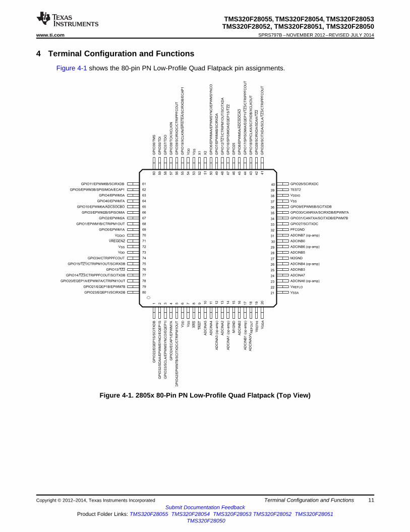
4 Terminal Configuration and Functions
Figure 4-1 shows the 80-pin PN Low-Profile Quad Flatpack pin assignments.
Figure 4-1. 2805x 80-Pin PN Low-Profile Quad Flatpack (Top View)
Copyright © 2012–2014, Texas Instruments Incorporated Terminal Configuration and Functions 11Submit Documentation Feedback
Product Folder Links: TMS320F28055 TMS320F28054 TMS320F28053 TMS320F28052 TMS320F28051TMS320F28050

TMS320F28055, TMS320F28054, TMS320F28053TMS320F28052, TMS320F28051, TMS320F28050SPRS797B –NOVEMBER 2012–REVISED JULY 2014 www.ti.com
4.1 Signal DescriptionsTable 4-1 describes the signals. With the exception of the JTAG pins, the GPIO function is the default atreset, unless otherwise mentioned. The peripheral signals that are listed under them are alternatefunctions. Some peripheral functions may not be available in all devices. See Table 3-1 for details. Inputsare not 5-V tolerant. All GPIO pins are I/O/Z and have an internal pullup (PU), which can be selectivelyenabled or disabled on a per-pin basis. This feature only applies to the GPIO pins. The pullups on thePWM pins are not enabled at reset. The pullups on other GPIO pins are enabled upon reset.
NOTE: When the on-chip VREG is used, the GPIO19, GPIO34, GPIO35, GPIO36, GPIO37, and GPIO38pins could glitch during power up. If this behavior is unacceptable in an application, 1.8 V could besupplied externally. There is no power-sequencing requirement when using an external 1.8-V supply.However, if the 3.3-V transistors in the level-shifting output buffers of the I/O pins are powered prior to the1.9-V transistors, it is possible for the output buffers to turn on, causing a glitch to occur on the pin duringpower up. To avoid this behavior, power the VDD pins prior to or simultaneously with the VDDIO pins,ensuring that the VDD pins have reached 0.7 V before the VDDIO pins reach 0.7 V.
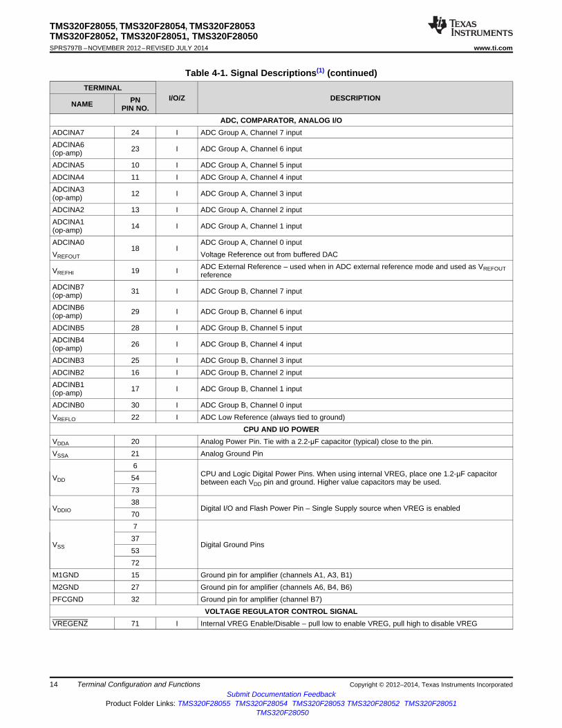
Table 4-1. Signal Descriptions(1)
TERMINALI/O/Z DESCRIPTIONPNNAME PIN NO.
JTAGJTAG test reset with internal pulldown (PD). TRST, when driven high, gives the scan systemcontrol of the operations of the device. If this signal is not connected or driven low, the deviceoperates in its functional mode, and the test reset signals are ignored. NOTE: TRST is anactive high test pin and must be maintained low at all times during normal device operation.
TRST 9 I An external pull-down resistor is required on this pin. The value of this resistor should bebased on drive strength of the debugger pods applicable to the design. A 2.2-kΩ resistorgenerally offers adequate protection. Since the value of the resistor is application-specific, TIrecommends that each target board be validated for proper operation of the debugger and theapplication. (↓)
SeeTCK I See GPIO38. JTAG test clock with internal pullup. (↑)GPIO38See See GPIO36. JTAG test-mode select (TMS) with internal pullup. This serial control input isTMS IGPIO36 clocked into the TAP controller on the rising edge of TCK.. (↑)See See GPIO35. JTAG test data input (TDI) with internal pullup. TDI is clocked into the selectedTDI IGPIO35 register (instruction or data) on a rising edge of TCK. (↑)See See GPIO37. JTAG scan out, test data output (TDO). The contents of the selected registerTDO O/ZGPIO37 (instruction or data) are shifted out of TDO on the falling edge of TCK. (8 mA drive)
FLASHTEST2 39 I/O Test Pin. Reserved for TI. Must be left unconnected.
12 Terminal Configuration and Functions Copyright © 2012–2014, Texas Instruments IncorporatedSubmit Documentation Feedback
Product Folder Links: TMS320F28055 TMS320F28054 TMS320F28053 TMS320F28052 TMS320F28051TMS320F28050

TMS320F28055, TMS320F28054, TMS320F28053TMS320F28052, TMS320F28051, TMS320F28050
www.ti.com SPRS797B –NOVEMBER 2012–REVISED JULY 2014
Table 4-1. Signal Descriptions(1) (continued)TERMINAL
I/O/Z DESCRIPTIONPNNAME PIN NO.CLOCK
See GPIO18. Output clock derived from SYSCLKOUT. XCLKOUT is either the samefrequency, one-half the frequency, or one-fourth the frequency of SYSCLKOUT. The value ofSeeXCLKOUT O/Z XCLKOUT is controlled by bits 1:0 (XCLKOUTDIV) in the XCLK register. At reset, XCLKOUTGPIO18 = SYSCLKOUT/4. The XCLKOUT signal can be turned off by setting XCLKOUTDIV to 3. Themux control for GPIO18 must also be set to XCLKOUT for this signal to propogate to the pin.See GPIO19 and GPIO38. External oscillator input. Pin source for the clock is controlled bythe XCLKINSEL bit in the XCLK register, GPIO38 is the default selection. This pin feeds aclock from an external 3.3-V oscillator. In this case, the X1 pin, if available, must be tied to
See GND and the on-chip crystal oscillator must be disabled via bit 14 in the CLKCTL register. If aGPIO19 crystal/resonator is used, the XCLKIN path must be disabled by bit 13 in the CLKCTL register.XCLKIN Iand NOTE: Designs that use the GPIO38/TCK/XCLKIN pin to supply an external clock for normalGPIO38 device operation may need to incorporate some hooks to disable this path during debug using
the JTAG connector. This action is to prevent contention with the TCK signal, which is activeduring JTAG debug sessions. The zero-pin internal oscillators may be used during this time toclock the device.On-chip crystal-oscillator input. To use this oscillator, a quartz crystal or a ceramic resonator
X1 52 I must be connected across X1 and X2. In this case, the XCLKIN path must be disabled by bit13 in the CLKCTL register. If this pin is not used, this pin must be tied to GND. (I)On-chip crystal-oscillator output. A quartz crystal or a ceramic resonator must be connectedX2 51 O across X1 and X2. If X2 is not used, X2 must be left unconnected. (O)
RESETDevice Reset (in) and Watchdog Reset (out). Piccolo devices have a built-in power-on reset(POR) and brown-out reset (BOR) circuitry. During a power-on or brown-out condition, this pinis driven low by the device. An external circuit may also drive this pin to assert a device reset.This pin is also driven low by the MCU when a watchdog reset occurs. During watchdog reset,the XRS pin is driven low for the watchdog reset duration of 512 OSCCLK cycles. A resistorbetween 2.2 kΩ and 10 kΩ should be placed between XRS and VDDIO. If a capacitor is placedXRS 8 I/OD between XRS and VSS for noise filtering, it should be 100 nF or smaller. These values willallow the watchdog to properly drive the XRS pin to VOL within 512 OSCCLK cycles when thewatchdog reset is asserted. Regardless of the source, a device reset causes the device toterminate execution. The program counter points to the address contained at the location0x3F FFC0. When reset is deactivated, execution begins at the location designated by theprogram counter. The output buffer of this pin is an open-drain with an internal pullup. (↑)
Copyright © 2012–2014, Texas Instruments Incorporated Terminal Configuration and Functions 13Submit Documentation Feedback
Product Folder Links: TMS320F28055 TMS320F28054 TMS320F28053 TMS320F28052 TMS320F28051TMS320F28050
TMS320F28055, TMS320F28054, TMS320F28053TMS320F28052, TMS320F28051, TMS320F28050SPRS797B –NOVEMBER 2012–REVISED JULY 2014 www.ti.com
Table 4-1. Signal Descriptions(1) (continued)TERMINAL
I/O/Z DESCRIPTIONPNNAME PIN NO.ADC, COMPARATOR, ANALOG I/O
ADCINA7 24 I ADC Group A, Channel 7 inputADCINA6 23 I ADC Group A, Channel 6 input(op-amp)ADCINA5 10 I ADC Group A, Channel 5 inputADCINA4 11 I ADC Group A, Channel 4 inputADCINA3 12 I ADC Group A, Channel 3 input(op-amp)ADCINA2 13 I ADC Group A, Channel 2 inputADCINA1 14 I ADC Group A, Channel 1 input(op-amp)ADCINA0 ADC Group A, Channel 0 input
18 IVREFOUT Voltage Reference out from buffered DAC
ADC External Reference – used when in ADC external reference mode and used as VREFOUTVREFHI 19 I referenceADCINB7 31 I ADC Group B, Channel 7 input(op-amp)ADCINB6 29 I ADC Group B, Channel 6 input(op-amp)ADCINB5 28 I ADC Group B, Channel 5 inputADCINB4 26 I ADC Group B, Channel 4 input(op-amp)ADCINB3 25 I ADC Group B, Channel 3 inputADCINB2 16 I ADC Group B, Channel 2 inputADCINB1 17 I ADC Group B, Channel 1 input(op-amp)ADCINB0 30 I ADC Group B, Channel 0 inputVREFLO 22 I ADC Low Reference (always tied to ground)
CPU AND I/O POWERVDDA 20 Analog Power Pin. Tie with a 2.2-μF capacitor (typical) close to the pin.VSSA 21 Analog Ground Pin
6CPU and Logic Digital Power Pins. When using internal VREG, place one 1.2-µF capacitorVDD 54 between each VDD pin and ground. Higher value capacitors may be used.
7338
VDDIO Digital I/O and Flash Power Pin – Single Supply source when VREG is enabled70737
VSS Digital Ground Pins5372
M1GND 15 Ground pin for amplifier (channels A1, A3, B1)M2GND 27 Ground pin for amplifier (channels A6, B4, B6)PFCGND 32 Ground pin for amplifier (channel B7)
VOLTAGE REGULATOR CONTROL SIGNALVREGENZ 71 I Internal VREG Enable/Disable – pull low to enable VREG, pull high to disable VREG
14 Terminal Configuration and Functions Copyright © 2012–2014, Texas Instruments IncorporatedSubmit Documentation Feedback
Product Folder Links: TMS320F28055 TMS320F28054 TMS320F28053 TMS320F28052 TMS320F28051TMS320F28050

TMS320F28055, TMS320F28054, TMS320F28053TMS320F28052, TMS320F28051, TMS320F28050
www.ti.com SPRS797B –NOVEMBER 2012–REVISED JULY 2014
Table 4-1. Signal Descriptions(1) (continued)TERMINAL
I/O/Z DESCRIPTIONPNNAME PIN NO.GPIO AND PERIPHERAL SIGNALS(2)
GPIO0 I/O/Z General-purpose input/output 069
EPWM1A O Enhanced PWM1 Output AGPIO1 I/O/Z General-purpose input/output 1EPWM1B 68 O Enhanced PWM1 Output BCTRIPM1OUT O CTRIPM1 CTRIPxx outputGPIO2 I/O/Z General-purpose input/output 2
67EPWM2A O Enhanced PWM2 Output AGPIO3 I/O/Z General-purpose input/output 3EPWM2B 66 O Enhanced PWM2 Output BSPISOMIA I/O SPI-A slave out, master inGPIO4 I/O/Z General-purpose input/output 4
63EPWM3A O Enhanced PWM3 output AGPIO5 I/O/Z General-purpose input/output 5EPWM3B O Enhanced PWM3 output B
62SPISIMOA I/O SPI-A slave in, master outECAP1 I/O Enhanced Capture input/output 1GPIO6 I/O/Z General-purpose input/output 6EPWM4A O Enhanced PWM4 output A
50EPWMSYNCI I External ePWM sync pulse inputEPWMSYNCO O External ePWM sync pulse outputGPIO7 I/O/Z General-purpose input/output 7EPWM4B 49 O Enhanced PWM4 output BSCIRXDA I SCI-A receive dataGPIO8 I/O/Z General-purpose input/output 8EPWM5A 45 O Enhanced PWM5 output AADCSOCAO O ADC start-of-conversion AGPIO9 I/O/Z General-purpose input/output 9EPWM5B 36 O Enhanced PWM5 output BSCITXDB O SCI-B transmit dataGPIO10 I/O/Z General-purpose input/output 10EPWM6A 65 O Enhanced PWM6 output AADCSOCBO O ADC start-of-conversion BGPIO11 I/O/Z General-purpose input/output 11EPWM6B 61 O Enhanced PWM6 output BSCIRXDB I SCI-B receive dataGPIO12 I/O/Z General-purpose input/output 12TZ1 I Trip Zone input 1
48CTRIPM1OUT O CTRIPM1 CTRIPxx outputSCITXDA O SCI-A transmit dataGPIO13 I/O/Z General-purpose input/output 13
76TZ2 I Trip zone input 2
Copyright © 2012–2014, Texas Instruments Incorporated Terminal Configuration and Functions 15Submit Documentation Feedback
Product Folder Links: TMS320F28055 TMS320F28054 TMS320F28053 TMS320F28052 TMS320F28051TMS320F28050

TMS320F28055, TMS320F28054, TMS320F28053TMS320F28052, TMS320F28051, TMS320F28050SPRS797B –NOVEMBER 2012–REVISED JULY 2014 www.ti.com
Table 4-1. Signal Descriptions(1) (continued)TERMINAL
I/O/Z DESCRIPTIONPNNAME PIN NO.GPIO14 I/O/Z General-purpose input/output 14TZ3 I Trip zone input 3
77CTRIPPFCOUT O CTRIPPFC outputSCITXDB O SCI-B transmit dataGPIO15 I/O/Z General-purpose input/output 15TZ1 I Trip zone input 1
75CTRIPM1OUT O CTRIPM1 CTRIPxx outputSCIRXDB I SCI-B receive dataGPIO16 I/O/Z General-purpose input/output 16SPISIMOA I/O SPI-A slave in, master out
47EQEP1S I/O Enhanced QEP1 strobeTZ2 I Trip Zone input 2GPIO17 I/O/Z General-purpose input/output 17SPISOMIA I/O SPI-A slave out, master inEQEP1I 44 I/O Enhanced QEP1 indexTZ3 I Trip zone input 3CTRIPPFCOUT O CTRIPPFC outputGPIO18 I/O/Z General-purpose input/output 18SPICLKA I/O SPI-A clock input/outputSCITXDB O SCI-B transmit data
43XCLKOUT O/Z Output clock derived from SYSCLKOUT. XCLKOUT is either the same frequency, one-half thefrequency, or one-fourth the frequency of SYSCLKOUT. The value of XCLKOUT is controlledby bits 1:0 (XCLKOUTDIV) in the XCLK register. At reset, XCLKOUT = SYSCLKOUT/4. TheXCLKOUT signal can be turned off by setting XCLKOUTDIV to 3. The mux control for GPIO18must also be set to XCLKOUT for this signal to propogate to the pin.
GPIO19 I/O/Z General-purpose input/output 19XCLKIN I External Oscillator Input. The path from this pin to the clock block is not gated by the mux
function of this pin. Care must be taken not to enable this path for clocking if this path is beingused for the other periperhal functions55
SPISTEA I/O SPI-A slave transmit enable input/outputSCIRXDB I SCI-B receive dataECAP1 I/O Enhanced Capture input/output 1GPIO20 I/O/Z General-purpose input/output 20EQEP1A I Enhanced QEP1 input A
78EPWM7A O Enhanced PWM7 output ACTRIPM1OUT O CTRIPM1 CTRIPxx outputGPIO21 I/O/Z General-purpose input/output 21EQEP1B 79 I Enhanced QEP1 input BEPWM7B O Enhanced PWM7 output BGPIO22 I/O/Z General-purpose input/output 22EQEP1S 1 I/O Enhanced QEP1 strobeSCITXDB O SCI-B transmit dataGPIO23 I/O/Z General-purpose input/output 23EQEP1I 80 I/O Enhanced QEP1 indexSCIRXDB I SCI-B receive data
16 Terminal Configuration and Functions Copyright © 2012–2014, Texas Instruments IncorporatedSubmit Documentation Feedback
Product Folder Links: TMS320F28055 TMS320F28054 TMS320F28053 TMS320F28052 TMS320F28051TMS320F28050

TMS320F28055, TMS320F28054, TMS320F28053TMS320F28052, TMS320F28051, TMS320F28050
www.ti.com SPRS797B –NOVEMBER 2012–REVISED JULY 2014
Table 4-1. Signal Descriptions(1) (continued)TERMINAL
I/O/Z DESCRIPTIONPNNAME PIN NO.GPIO24 I/O/Z General-purpose input/output 24ECAP1 4 I/O Enhanced Capture input/output 1EPWM7A O Enhanced PWM7 output AGPIO25 46 I/O/Z General-purpose input/output 25GPIO26 I/O/Z General-purpose input/output 26
40SCIRXDC I SCI-C receive dataGPIO27 I/O/Z General-purpose input/output 27
33SCITXDC O SCI-C transmit dataGPIO28 I/O/Z General-purpose input/output 28SCIRXDA I SCI-A receive data
42SDAA I/OC I2C data open-drain bidirectional portTZ2 I Trip zone input 2GPIO29 I/O/Z General-purpose input/output 29SCITXDA O SCI-A transmit dataSCLA 41 I/OC I2C clock open-drain bidirectional portTZ3 I Trip zone input 3CTRIPPFCOUT O CTRIPPFC outputGPIO30 I/O/Z General-purpose input/output 30CANRXA I CAN receive
35SCIRXDB I SCI-B receive dataEPWM7A O Enhanced PWM7 output AGPIO31 I/O/Z General-purpose input/output 31CANTXA O CAN transmit
34SCITXDB O SCI-B transmit dataEPWM7B O Enhanced PWM7 output BGPIO32 I/O/Z General-purpose input/output 32SDAA I/OC I2C data open-drain bidirectional port
2EPWMSYNCI I Enhanced PWM external sync pulse inputEQEP1S I/O Enhanced QEP1 strobeGPIO33 I/O/Z General-Purpose Input/Output 33SCLA I/OC I2C clock open-drain bidirectional port
3EPWMSYNCO O Enhanced PWM external synch pulse outputEQEP1I I/O Enhanced QEP1 indexGPIO34 I/O/Z General-Purpose Input/Output 34
74CTRIPPFCOUT O CTRIPPFC outputGPIO35 I/O/Z General-Purpose Input/Output 35
59TDI I JTAG test data input (TDI) with internal pullup. TDI is clocked into the selected register(instruction or data) on a rising edge of TCK
GPIO36 I/O/Z General-Purpose Input/Output 3660TMS I JTAG test-mode select (TMS) with internal pullup. This serial control input is clocked into the
TAP controller on the rising edge of TCK.GPIO37 I/O/Z General-Purpose Input/Output 37
58TDO O/Z JTAG scan out, test data output (TDO). The contents of the selected register (instruction ordata) are shifted out of TDO on the falling edge of TCK (8 mA drive)
Copyright © 2012–2014, Texas Instruments Incorporated Terminal Configuration and Functions 17Submit Documentation Feedback
Product Folder Links: TMS320F28055 TMS320F28054 TMS320F28053 TMS320F28052 TMS320F28051TMS320F28050

TMS320F28055, TMS320F28054, TMS320F28053TMS320F28052, TMS320F28051, TMS320F28050SPRS797B –NOVEMBER 2012–REVISED JULY 2014 www.ti.com
Table 4-1. Signal Descriptions(1) (continued)TERMINAL
I/O/Z DESCRIPTIONPNNAME PIN NO.GPIO38 I/O/Z General-Purpose Input/Output 38TCK I JTAG test clock with internal pullup
57XCLKIN I External Oscillator Input. The path from this pin to the clock block is not gated by the muxfunction of this pin. Care must be taken to not enable this path for clocking if this path is beingused for the other functions.
GPIO39 I/O/Z General-Purpose Input/Output 39SCIRXDC 56 I SCI-C receive dataCTRIPPFCOUT O CTRIPPFC outputGPIO40 I/O/Z General-Purpose Input/Output 40. Internal pullup enabled by default.
64EPWM7A O Enhanced PWM7 output AGPIO42 I/O/Z General-Purpose Input/Output 42EPWM7B O Enhanced PWM7 output B
5SCITXDC O SCI-C transmit dataCTRIPM1OUT O CTRIPM1 CTRIPxx output
(1) I = Input, O = Output, Z = High Impedance, OC = Open Collector, OD = Open Drain, ↑ = Pullup, ↓ = Pulldown(2) The GPIO function (shown in bold italics) is the default at reset. The peripheral signals that are listed under them are alternate functions.
For JTAG pins that have the GPIO functionality multiplexed, the input path to the GPIO block is always valid. The output path from theGPIO block and the path to the JTAG block from a pin is enabled or disabled based on the condition of the TRST signal. See theSystem Control and Interrupts chapter of the TMS320x2805x Piccolo Technical Reference Manual (SPRUHE5) for details.
18 Terminal Configuration and Functions Copyright © 2012–2014, Texas Instruments IncorporatedSubmit Documentation Feedback
Product Folder Links: TMS320F28055 TMS320F28054 TMS320F28053 TMS320F28052 TMS320F28051TMS320F28050

TMS320F28055, TMS320F28054, TMS320F28053TMS320F28052, TMS320F28051, TMS320F28050
www.ti.com SPRS797B –NOVEMBER 2012–REVISED JULY 2014
5 Specifications
5.1 Absolute Maximum Ratings (1) (2)
Supply voltage range, VDDIO (I/O and Flash) with respect to VSS –0.3 V to 4.6 VSupply voltage range, VDD with respect to VSS –0.3 V to 2.5 VAnalog voltage range, VDDA with respect to VSSA –0.3 V to 4.6 VInput voltage range, VIN (3.3 V) –0.3 V to 4.6 VOutput voltage range, VO –0.3 V to 4.6 VInput clamp current, IIK (VIN < 0 or VIN > VDDIO) (3) ±20 mAOutput clamp current, IOK (VO < 0 or VO > VDDIO) ±20 mAJunction temperature range, TJ
(4) –40°C to 150°C
(1) Stresses beyond those listed under Absolute Maximum Ratings may cause permanent damage to the device. These are stress ratingsonly, and functional operation of the device at these or any other conditions beyond those indicated under Section 5.3 is not implied.Exposure to absolute-maximum-rated conditions for extended periods may affect device reliability.
(2) All voltage values are with respect to VSS, unless otherwise noted.(3) Continuous clamp current per pin is ± 2 mA.(4) Long-term high-temperature storage or extended use at maximum temperature conditions may result in a reduction of overall device life.
For additional information, see IC Package Thermal Metrics Application Report (SPRA953).
5.2 Handling RatingsMIN MAX UNIT
Tstg Storage temperature range (1) –65 150 °CHuman Body Model (HBM), per AEC Q100-002 (3) –2 2 kV
Electrostatic All pins –500 500 VVESD discharge (ESD) (2) Charged Device Model (CDM),Corner pins on 80-pin PN:performance per AEC Q100-011 –750 750 V1, 20, 21, 40, 41, 60, 61, 80
(1) Long-term high-temperature storage or extended use at maximum temperature conditions may result in a reduction of overall device life.For additional information, see the IC Package Thermal Metrics Application Report (SPRA953).
(2) ESD measures device sensitivity/immunity to damage caused by assembly line electrostatic discharges into the device.(3) AEC Q100-002 indicates HBM stressing is done in accordance with the ANSI/ESDA/JEDEC JS-001 specification.
Copyright © 2012–2014, Texas Instruments Incorporated Specifications 19Submit Documentation Feedback
Product Folder Links: TMS320F28055 TMS320F28054 TMS320F28053 TMS320F28052 TMS320F28051TMS320F28050

TMS320F28055, TMS320F28054, TMS320F28053TMS320F28052, TMS320F28051, TMS320F28050SPRS797B –NOVEMBER 2012–REVISED JULY 2014 www.ti.com
5.3 Recommended Operating ConditionsMIN NOM MAX UNIT
Device supply voltage, I/O, VDDIO(1) 2.97 3.3 3.63 V
Device supply voltage CPU, VDD (When internal 1.71 1.8 1.995 VVREG is disabled and 1.8 V is supplied externally)Supply ground, VSS 0 VAnalog supply voltage, VDDA
(1) 2.97 3.3 3.63 VAnalog ground, VSSA 0 VDevice clock frequency (system clock) 2 60 MHzHigh-level input voltage, VIH (3.3 V) 2 VDDIO + 0.3 VLow-level input voltage, VIL (3.3 V) VSS – 0.3 0.8 VHigh-level output source current, VOH = VOH(MIN) , IOH All GPIO pins –4 mA
Group 2 (2) –8 mALow-level output sink current, VOL = VOL(MAX), IOL All GPIO pins 4 mA
Group 2 (2) 8 mAJunction temperature, TJ T version –40 105
S version –40 125 °CQ version (Q100 qualification) –40 125
(1) VDDIO and VDDA should be maintained within approximately 0.3 V of each other.(2) Group 2 pins are as follows: GPIO16, GPIO17, GPIO18, GPIO28, GPIO29, GPIO30, GPIO31, GPIO36, GPIO37
5.4 Electrical Characteristics (1)
Over Recommended Operating Conditions (Unless Otherwise Noted)PARAMETER TEST CONDITIONS MIN TYP MAX UNIT
IOH = IOH MAX 2.4VOH High-level output voltage V
IOH = 50 μA VDDIO – 0.2VOL Low-level output voltage IOL = IOL MAX 0.4 V
All GPIO pins –80 –140 –205Pin with pullup VDDIO = 3.3 V, VIN = 0 VenabledInput current XRS pin –230 –300 –375IIL μA(low level) Pin with pulldown VDDIO = 3.3 V, VIN = 0 V ±2enabledPin with pullup VDDIO = 3.3 V, VIN = VDDIO ±2enabledInput currentIIH μA(high level) Pin with pulldown VDDIO = 3.3 V, VIN = VDDIO 28 50 80enabled
Output current, pullup orIOZ VO = VDDIO or 0 V ±2 μApulldown disabledCI Input capacitance 2 pF
VDDIO BOR trip point Falling VDDIO 2.78 VVDDIO BOR hysteresis 35 mVSupervisor reset release delay Time after BOR/POR/OVR event is removed to XRS 400 800 μstime releaseVREG VDD output Internal VREG on 1.9 V
(1) When the on-chip VREG is used, its output is monitored by the POR/BOR circuit, which will reset the device should the core voltage(VDD) go out of range.
20 Specifications Copyright © 2012–2014, Texas Instruments IncorporatedSubmit Documentation Feedback
Product Folder Links: TMS320F28055 TMS320F28054 TMS320F28053 TMS320F28052 TMS320F28051TMS320F28050

TMS320F28055, TMS320F28054, TMS320F28053TMS320F28052, TMS320F28051, TMS320F28050
www.ti.com SPRS797B –NOVEMBER 2012–REVISED JULY 2014
5.5 Thermal Resistance Characteristics for PN Package°C/W (1) AIR FLOW (lfm) (2)
RΘJC Junction-to-case thermal resistance 14.2 0RΘJB Junction-to-board thermal resistance 21.9 0
49.9 038.3 150RΘJA Junction-to-free air thermal resistance(High k PCB) 36.7 25034.4 5000.8 01.18 150
PsiJT Junction-to-package top1.34 2501.62 50021.6 020.7 150
PsiJB Junction-to-board20.5 25020.1 500
(1) These values are based on a JEDEC defined 2S2P system (with the exception of the Theta JC [RΘJC] value, which is based on aJEDEC defined 1S0P system) and will change based on environment as well as application. For more information, see theseEIA/JEDEC standards:• JESD51-2, Integrated Circuits Thermal Test Method Environmental Conditions - Natural Convection (Still Air)• JESD51-3, Low Effective Thermal Conductivity Test Board for Leaded Surface Mount Packages• JESD51-7, High Effective Thermal Conductivity Test Board for Leaded Surface Mount Packages• JESD51-9, Test Boards for Area Array Surface Mount Package Thermal Measurements
(2) lfm = linear feet per minute
5.6 Thermal Design ConsiderationsBased on the end application design and operational profile, the IDD and IDDIO currents could vary.Systems that exceed the recommended maximum power dissipation in the end product may requireadditional thermal enhancements. Ambient temperature (TA) varies with the end application and productdesign. The critical factor that affects reliability and functionality is TJ, the junction temperature, not theambient temperature. Hence, care should be taken to keep TJ within the specified limits. Tcase should bemeasured to estimate the operating junction temperature TJ. Tcase is normally measured at the center ofthe package top-side surface. The thermal application report IC Package Thermal Metrics (SPRA953)helps to understand the thermal metrics and definitions.
Copyright © 2012–2014, Texas Instruments Incorporated Specifications 21Submit Documentation Feedback
Product Folder Links: TMS320F28055 TMS320F28054 TMS320F28053 TMS320F28052 TMS320F28051TMS320F28050
TRST
TMS
TDI
TDO
TCK
VDDIO
MCU
EMU0
EMU1
TRST
TMS
TDI
TDO
TCK
TCK_RET
13
14
2
1
3
7
11
9
6 inches or less
PD
GND
GND
GND
GND
GND
5
4
6
8
10
12
JTAG Header
VDDIO
TMS320F28055, TMS320F28054, TMS320F28053TMS320F28052, TMS320F28051, TMS320F28050SPRS797B –NOVEMBER 2012–REVISED JULY 2014 www.ti.com
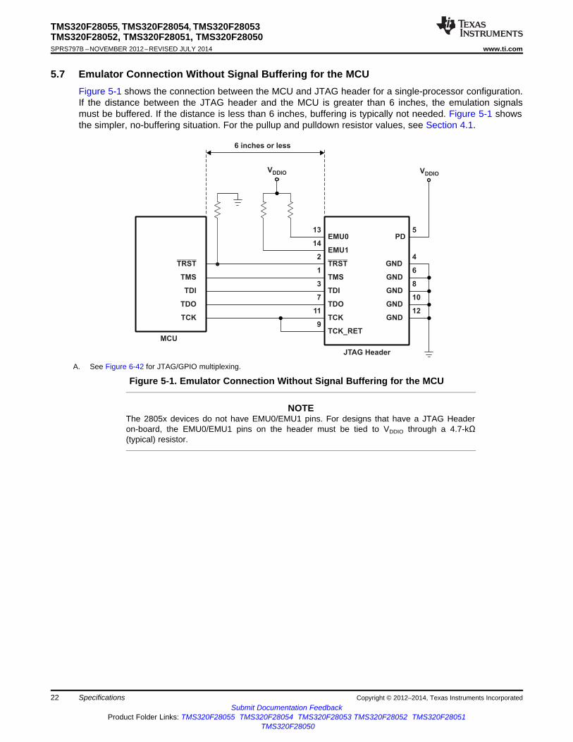
5.7 Emulator Connection Without Signal Buffering for the MCUFigure 5-1 shows the connection between the MCU and JTAG header for a single-processor configuration.If the distance between the JTAG header and the MCU is greater than 6 inches, the emulation signalsmust be buffered. If the distance is less than 6 inches, buffering is typically not needed. Figure 5-1 showsthe simpler, no-buffering situation. For the pullup and pulldown resistor values, see Section 4.1.
A. See Figure 6-42 for JTAG/GPIO multiplexing.
Figure 5-1. Emulator Connection Without Signal Buffering for the MCU
NOTEThe 2805x devices do not have EMU0/EMU1 pins. For designs that have a JTAG Headeron-board, the EMU0/EMU1 pins on the header must be tied to VDDIO through a 4.7-kΩ(typical) resistor.
22 Specifications Copyright © 2012–2014, Texas Instruments IncorporatedSubmit Documentation Feedback
Product Folder Links: TMS320F28055 TMS320F28054 TMS320F28053 TMS320F28052 TMS320F28051TMS320F28050

TMS320F28055, TMS320F28054, TMS320F28053TMS320F28052, TMS320F28051, TMS320F28050
www.ti.com SPRS797B –NOVEMBER 2012–REVISED JULY 2014
5.8 Current Consumption
Table 5-1. TMS320F2805x Current Consumption at 60-MHz SYSCLKOUT
VREG ENABLED VREG DISABLED
MODE TEST CONDITIONS IDDIO(1) IDDA
(2) IDD IDDIO(1) IDDA
(2)
TYP(3) MAX TYP(3) MAX TYP(3) MAX TYP(3) MAX TYP(3) MAX
The following peripheral clocks areenabled:• ePWM1, ePWM2, ePWM3,
ePWM4, ePWM5, ePWM6,ePWM7
• eCAP1• eQEP1• eCAN-A• CLA• SCI-A, SCI-B, SCI-C
Operational • SPI-A 95 mA(6) 132 mA 40 mA 60 mA 85 mA(6) 110 mA 14 mA 25 mA 40 mA 60 mA(Flash) • ADC• I2C-A• COMPA1, COMPA3,
COMPB1, COMPB7• CPU-TIMER0,
CPU-TIMER1,CPU-TIMER2
All PWM pins are toggled at 60 kHz.All I/O pins are left unconnected.(4)(5)
Code is running out of flash with2 wait-states.XCLKOUT is turned off.
Flash is powered down.IDLE XCLKOUT is turned off. 14 mA 27 mA 15 μA 25 μA 14 mA 27 mA 120 μA 450 μA 15 μA 25 μA
All peripheral clocks are turned off.
Flash is powered down.STANDBY 9 mA 15 mA 15 μA 25 μA 9 mA 15 mA 120 μA 450 μA 15 μA 25 μAPeripheral clocks are off.
Flash is powered down.HALT Peripheral clocks are off. 300 μA 15 μA 25 μA 50 μA 24 μA 15 μA 25 μA
Input clock is disabled. (7)
(1) IDDIO current is dependent on the electrical loading on the I/O pins.(2) In order to realize the IDDA currents shown for IDLE, STANDBY, and HALT, clock to the ADC module must be turned off explicitly by
writing to the PCLKCR0 register.(3) The TYP numbers are applicable over room temperature and nominal voltage.(4) The following is done in a loop:
• Data is continuously transmitted out of SPI-A, SCI-A, SCI-B, SCI-C, eCAN-A, and I2C-A ports.• The hardware multiplier is exercised.• Watchdog is reset.• ADC is performing continuous conversion.• GPIO17 is toggled.
(5) CLA is continuously performing polynomial calculations.(6) For F2805x devices that do not have CLA, subtract the IDD current number for CLA (see Table 5-2) from the IDD (VREG disabled)/IDDIO
(VREG enabled) current numbers shown in Table 5-1 for operational mode.(7) If a quartz crystal or ceramic resonator is used as the clock source, the HALT mode shuts down the on-chip crystal oscillator.
NOTEThe peripheral-I/O multiplexing implemented in the device prevents all available peripheralsfrom being used at the same time because more than one peripheral function may share anI/O pin. It is, however, possible to turn on the clocks to all the peripherals at the same time,although such a configuration is not useful. If the clocks to all the peripherals are turned onat the same time, the current drawn by the device will be more than the numbers specified inthe current consumption tables.
Copyright © 2012–2014, Texas Instruments Incorporated Specifications 23Submit Documentation Feedback
Product Folder Links: TMS320F28055 TMS320F28054 TMS320F28053 TMS320F28052 TMS320F28051TMS320F28050

TMS320F28055, TMS320F28054, TMS320F28053TMS320F28052, TMS320F28051, TMS320F28050SPRS797B –NOVEMBER 2012–REVISED JULY 2014 www.ti.com
5.8.1 Reducing Current ConsumptionThe 2805x devices incorporate a method to reduce the device current consumption. Since each peripheralunit has an individual clock-enable bit, significant reduction in current consumption can be achieved byturning off the clock to any peripheral module that is not used in a given application. Furthermore, any oneof the three low-power modes could be taken advantage of to reduce the current consumption evenfurther. Table 5-2 indicates the typical reduction in current consumption achieved by turning off the clocks.
Table 5-2. Typical Current Consumption by VariousPeripherals (at 60 MHz) (1)
PERIPHERAL IDD CURRENTMODULE (2) REDUCTION (mA)
ADC 2 (3)
I2C 3ePWM 2eCAP 2eQEP 2SCI 2SPI 2
COMP/DAC 1PGA 2
CPU-TIMER 1Internal zero-pin oscillator 0.5
CAN 2.5CLA 20
(1) All peripheral clocks (except CPU Timer clock) are disabled uponreset. Writing to or reading from peripheral registers is possible onlyafter the peripheral clocks are turned on.
(2) For peripherals with multiple instances, the current quoted is permodule. For example, the 2 mA value quoted for ePWM is for oneePWM module.
(3) This number represents the current drawn by the digital portion ofthe ADC module. Turning off the clock to the ADC module results inthe elimination of the current drawn by the analog portion of the ADC(IDDA) as well.
NOTEIDDIO current consumption is reduced by 15 mA (typical) when XCLKOUT is turned off.
NOTEThe baseline IDD current (current when the core is executing a dummy loop with noperipherals enabled) is 40 mA, typical. To arrive at the IDD current for a given application, thecurrent-drawn by the peripherals (enabled by that application) must be added to the baselineIDD current.
Following are other methods to reduce power consumption further:• The flash module may be powered down if code is run off SARAM. This method results in a current
reduction of 18 mA (typical) in the VDD rail and 13 mA (typical) in the VDDIO rail.• Savings in IDDIO may be realized by disabling the pullups on pins that assume an output function.
24 Specifications Copyright © 2012–2014, Texas Instruments IncorporatedSubmit Documentation Feedback
Product Folder Links: TMS320F28055 TMS320F28054 TMS320F28053 TMS320F28052 TMS320F28051TMS320F28050

Operational Power vs Frequency
200
250
300
350
400
450
500
0 10 20 30 40 50 60 70
SYSCLKOUT (MHz)
Op
era
tio
na
lP
ow
er
(mW
)
Operational Current vs Frequency
0
20
40
60
80
100
120
140
0 10 20 30 40 50 60 70
SYSCLKOUT (MHz)
Op
era
tio
nal
Cu
rren
t(m
A)
IDDIO IDDA
TMS320F28055, TMS320F28054, TMS320F28053TMS320F28052, TMS320F28051, TMS320F28050
www.ti.com SPRS797B –NOVEMBER 2012–REVISED JULY 2014
5.8.2 Current Consumption Graphs (VREG Enabled)
Figure 5-2. Typical Operational Current Versus Frequency (F2805x)
Figure 5-3. Typical Operational Power Versus Frequency (F2805x)
Copyright © 2012–2014, Texas Instruments Incorporated Specifications 25Submit Documentation Feedback
Product Folder Links: TMS320F28055 TMS320F28054 TMS320F28053 TMS320F28052 TMS320F28051TMS320F28050

Typical CLA operational current vs SYSCLKOUT
0
5
10
15
20
25
10 15 20 25 30 35 40 45 50 55 60
SYSCLKOUT (MHz)
CL
Ao
pe
rati
on
al
IDD
IOc
urr
en
t(m
A)
TMS320F28055, TMS320F28054, TMS320F28053TMS320F28052, TMS320F28051, TMS320F28050SPRS797B –NOVEMBER 2012–REVISED JULY 2014 www.ti.com
Figure 5-4. Typical CLA Operational Current Versus SYSCLKOUT
26 Specifications Copyright © 2012–2014, Texas Instruments IncorporatedSubmit Documentation Feedback
Product Folder Links: TMS320F28055 TMS320F28054 TMS320F28053 TMS320F28052 TMS320F28051TMS320F28050

Transmission Line
4.0 pF 1.85 pF
Z0 = 50 W(A)
Tester Pin Electronics Data Sheet Timing Reference Point
OutputUnderTest
42 W 3.5 nH
Device Pin(B)
TMS320F28055, TMS320F28054, TMS320F28053TMS320F28052, TMS320F28051, TMS320F28050
www.ti.com SPRS797B –NOVEMBER 2012–REVISED JULY 2014
5.9 Parameter Information
5.9.1 Timing Parameter SymbologyTiming parameter symbols used are created in accordance with JEDEC Standard 100. To shorten thesymbols, some of the pin names and other related terminology have been abbreviated as follows:
Lowercase subscripts and their Letters and symbols and theirmeanings: meanings:a access time H Highc cycle time (period) L Lowd delay time V Valid
Unknown, changing, or don't caref fall time X levelh hold time Z High impedancer rise timesu setup timet transition timev valid timew pulse duration (width)
5.9.2 General Notes on Timing ParametersAll output signals from the 28x devices (including XCLKOUT) are derived from an internal clock such thatall output transitions for a given half-cycle occur with a minimum of skewing relative to each other.
The signal combinations shown in the following timing diagrams may not necessarily represent actualcycles. For actual cycle examples, see the appropriate cycle description section of this document.
5.10 Test Load CircuitThis test load circuit is used to measure all switching characteristics provided in this document.
A. Input requirements in this data sheet are tested with an input slew rate of < 4 Volts per nanosecond (4 V/ns) at thedevice pin.
B. The data sheet provides timing at the device pin. For output timing analysis, the tester pin electronics and itstransmission line effects must be taken into account. A transmission line with a delay of 2 ns or longer can be used toproduce the desired transmission line effect. The transmission line is intended as a load only. It is not necessary toadd or subtract the transmission line delay (2 ns or longer) from the data sheet timing.
Figure 5-5. 3.3-V Test Load Circuit
Copyright © 2012–2014, Texas Instruments Incorporated Specifications 27Submit Documentation Feedback
Product Folder Links: TMS320F28055 TMS320F28054 TMS320F28053 TMS320F28052 TMS320F28051TMS320F28050

tw(RSL1)
th(boot-mode)(C)
V V
(3.3 V)DDIO DDA,
INTOSC1
X1/X2
XRS(D)
Boot-Mode
Pins
V (1.8 V)DD
XCLKOUT
I/O Pins
User-code dependent
User-code dependent
Boot-ROM execution startsPeripheral/GPIO function
Based on boot code
GPIO pins as input
GPIO pins as input (state depends on internal PU/PD)
(E)
tOSCST
User-code dependent
Address/Data/
Control
(Internal)
Address/data valid, internal boot-ROM code execution phase
User-code execution phasetd(EX)
tINTOSCST
(A)
(B)
TMS320F28055, TMS320F28054, TMS320F28053TMS320F28052, TMS320F28051, TMS320F28050SPRS797B –NOVEMBER 2012–REVISED JULY 2014 www.ti.com
5.11 Power SequencingThere is no power sequencing requirement needed to ensure the device is in the proper state after resetor to prevent the I/Os from glitching during power up or power down (GPIO19, GPIO34–38 do not haveglitch-free I/Os). No voltage larger than a diode drop (0.7 V) above VDDIO should be applied to any digitalpin (for analog pins, this value is 0.7 V above VDDA) prior to powering up the device. Voltages applied topins on an unpowered device can bias internal p-n junctions in unintended ways and produceunpredictable results.
A. Upon power up, SYSCLKOUT is OSCCLK/4. Since the XCLKOUTDIV bits in the XCLK register come up with a resetstate of 0, SYSCLKOUT is further divided by 4 before SYSCLKOUT appears at XCLKOUT. XCLKOUT = OSCCLK/16during this phase.
B. Boot ROM configures the DIVSEL bits for /1 operation. XCLKOUT = OSCCLK/4 during this phase. Note thatXCLKOUT will not be visible at the pin until explicitly configured by user code.
C. After reset, the boot ROM code samples Boot Mode pins. Based on the status of the Boot Mode pin, the boot codebranches to destination memory or boot code function. If boot ROM code executes after power-on conditions (indebugger environment), the boot code execution time is based on the current SYSCLKOUT speed. The SYSCLKOUTwill be based on user environment and could be with or without PLL enabled.
D. Using the XRS pin is optional due to the on-chip POR circuitry.E. The internal pullup or pulldown will take effect when BOR is driven high.
Figure 5-6. Power-on Reset
28 Specifications Copyright © 2012–2014, Texas Instruments IncorporatedSubmit Documentation Feedback
Product Folder Links: TMS320F28055 TMS320F28054 TMS320F28053 TMS320F28052 TMS320F28051TMS320F28050

th(boot-mode)(A)
tw(RSL2)
INTOSC1
X1/X2
XRS
Boot-Mode
Pins
XCLKOUT
I/O Pins
Address/Data/
Control
(Internal)
Boot-ROM Execution Starts
User-Code Execution Starts
User-Code Dependent
User-Code Execution Phase
User-Code Dependent
User-Code Execution
Peripheral/GPIO Function
User-Code Dependent
GPIO Pins as Input (State Depends on Internal PU/PD)
GPIO Pins as Input Peripheral/GPIO Function
td(EX)
TMS320F28055, TMS320F28054, TMS320F28053TMS320F28052, TMS320F28051, TMS320F28050
www.ti.com SPRS797B –NOVEMBER 2012–REVISED JULY 2014
Table 5-3. Reset (XRS) Timing RequirementsMIN MAX UNIT
th(boot-mode) Hold time for boot-mode pins 1000tc(SCO) cyclestw(RSL2) Pulse duration, XRS low on warm reset 32tc(OSCCLK) cycles
Table 5-4. Reset (XRS) Switching Characteristicsover recommended operating conditions (unless otherwise noted)
PARAMETER MIN TYP MAX UNITtw(RSL1) Pulse duration, XRS driven by device 600 μstw(WDRS) Pulse duration, reset pulse generated by watchdog 512tc(OSCCLK) cyclestd(EX) Delay time, address/data valid after XRS high 32tc(OSCCLK) cyclestINTOSCST Start up time, internal zero-pin oscillator 3 μstOSCST
(1) On-chip crystal-oscillator start-up time 1 10 ms
(1) Dependent on crystal/resonator and board design.
A. After reset, the Boot ROM code samples BOOT Mode pins. Based on the status of the Boot Mode pin, the boot codebranches to destination memory or boot code function. If Boot ROM code executes after power-on conditions (indebugger environment), the Boot code execution time is based on the current SYSCLKOUT speed. TheSYSCLKOUT will be based on user environment and could be with or without PLL enabled.
Figure 5-7. Warm Reset
Copyright © 2012–2014, Texas Instruments Incorporated Specifications 29Submit Documentation Feedback
Product Folder Links: TMS320F28055 TMS320F28054 TMS320F28053 TMS320F28052 TMS320F28051TMS320F28050

OSCCLK
SYSCLKOUT
Write to PLLCR
OSCCLK * 2
(Current CPU
Frequency)
OSCCLK/2
(CPU frequency while PLL is stabilizingwith the desired frequency. This period
(PLL lock-up time t ) is 1 ms long.)p
OSCCLK * 4
(Changed CPU frequency)
TMS320F28055, TMS320F28054, TMS320F28053TMS320F28052, TMS320F28051, TMS320F28050SPRS797B –NOVEMBER 2012–REVISED JULY 2014 www.ti.com
Figure 5-8 shows an example for the effect of writing into PLLCR register. In the first phase, PLLCR =0x0004 and SYSCLKOUT = OSCCLK x 2. The PLLCR is then written with 0x0008. Right after the PLLCRregister is written, the PLL lock-up phase begins. During this phase, SYSCLKOUT = OSCCLK/2. After thePLL lock-up is complete, SYSCLKOUT reflects the new operating frequency, OSCCLK x 4.
Figure 5-8. Example of Effect of Writing Into PLLCR Register
30 Specifications Copyright © 2012–2014, Texas Instruments IncorporatedSubmit Documentation Feedback
Product Folder Links: TMS320F28055 TMS320F28054 TMS320F28053 TMS320F28052 TMS320F28051TMS320F28050

TMS320F28055, TMS320F28054, TMS320F28053TMS320F28052, TMS320F28051, TMS320F28050
www.ti.com SPRS797B –NOVEMBER 2012–REVISED JULY 2014
5.12 Clock Specifications
5.12.1 Device Clock TableThis section provides the timing requirements and switching characteristics for the various clock optionsavailable on the 2805x MCUs. Table 5-5 lists the cycle times of various clocks.
Table 5-5. 2805x Clock Table and Nomenclature (60-MHz Devices)
MIN NOM MAX UNITtc(SCO), Cycle time 16.67 500 ns
SYSCLKOUTFrequency 2 60 MHztc(LCO), Cycle time 16.67 66.67 (2) ns
LSPCLK (1)Frequency 15 (2) 60 MHztc(ADCCLK), Cycle time 16.67 ns
ADC clockFrequency 60 MHz
(1) Lower LSPCLK will reduce device power consumption.(2) This value is the default reset value if SYSCLKOUT = 60 MHz.
Table 5-6. Device Clocking Requirements/Characteristics
MIN NOM MAX UNITtc(OSC), Cycle time 50 200 nsOn-chip oscillator (X1/X2 pins)
(Crystal/Resonator) Frequency 5 20 MHztc(CI), Cycle time (C8) 33.3 200 nsExternal oscillator/clock source
(XCLKIN pin) — PLL Enabled Frequency 5 30 MHztc(CI), Cycle time (C8) 33.33 250 nsExternal oscillator/clock source
(XCLKIN pin) — PLL Disabled Frequency 4 30 MHzLimp mode SYSCLKOUT Frequency range 1 to 5 MHz(with /2 enabled)
tc(XCO), Cycle time (C1) 66.67 2000 nsXCLKOUT
Frequency 0.5 15 MHzPLL lock time (1) tp 1 ms
(1) The PLLLOCKPRD register must be updated based on the number of OSCCLK cycles. If the zero-pin internal oscillators (10 MHz) areused as the clock source, then the PLLLOCKPRD register must be written with a value of 10,000 (minimum).
Copyright © 2012–2014, Texas Instruments Incorporated Specifications 31Submit Documentation Feedback
Product Folder Links: TMS320F28055 TMS320F28054 TMS320F28053 TMS320F28052 TMS320F28051TMS320F28050

Zero-Pin Oscillator Frequency Movement With Temperature
9.6
9.7
9.8
9.9
10
10.1
10.2
10.3
10.4
10.5
10.6
–40 –30 –20 –10 0 10 20 30 40 50 60 70 80 90 100 110 120
Temperature (°C)
Ou
tpu
t F
req
uen
cy (
MH
z)
Typical
Max
TMS320F28055, TMS320F28054, TMS320F28053TMS320F28052, TMS320F28051, TMS320F28050SPRS797B –NOVEMBER 2012–REVISED JULY 2014 www.ti.com
Table 5-7. Internal Zero-Pin Oscillator (INTOSC1, INTOSC2) Characteristics
PARAMETER MIN TYP MAX UNITInternal zero-pin oscillator 1 (INTOSC1) at 30°C (1) (2) Frequency 10.000 MHzInternal zero-pin oscillator 2 (INTOSC2) at 30°C (1) (2) Frequency 10.000 MHzAccuracy using oscillator compensation (1) (2) ±1 %Step size (coarse trim) 55 kHzStep size (fine trim) 14 kHzTemperature drift (3) 3.03 4.85 kHz/°CVoltage (VDD) drift (3) 175 Hz/mV
(1) In order to achieve better oscillator accuracy (10 MHz ± 1% or better) than shown, see the Oscillator Compensation Guide ApplicationReport (SPRAB84). Refer to Figure 5-9 for TYP and MAX values.
(2) Frequency range ensured only when VREG is enabled, VREGENZ = VSS.(3) Output frequency of the internal oscillators follows the direction of both the temperature gradient and voltage (VDD) gradient. For
example:• Increase in temperature will cause the output frequency to increase per the temperature coefficient.• Decrease in voltage (VDD) will cause the output frequency to decrease per the voltage coefficient.
Figure 5-9. Zero-Pin Oscillator Frequency Movement With Temperature
32 Specifications Copyright © 2012–2014, Texas Instruments IncorporatedSubmit Documentation Feedback
Product Folder Links: TMS320F28055 TMS320F28054 TMS320F28053 TMS320F28052 TMS320F28051TMS320F28050

C4
C3
XCLKOUT(B)
XCLKIN(A)
C5
C9C10
C1
C8
C6
TMS320F28055, TMS320F28054, TMS320F28053TMS320F28052, TMS320F28051, TMS320F28050
www.ti.com SPRS797B –NOVEMBER 2012–REVISED JULY 2014
5.12.2 Clock Requirements and Characteristics
Table 5-8. XCLKIN Timing Requirements - PLL EnabledNO. MIN MAX UNITC9 tf(CI) Fall time, XCLKIN 6 nsC10 tr(CI) Rise time, XCLKIN 6 nsC11 tw(CIL) Pulse duration, XCLKIN low as a percentage of tc(OSCCLK) 45 55 %C12 tw(CIH) Pulse duration, XCLKIN high as a percentage of tc(OSCCLK) 45 55 %
Table 5-9. XCLKIN Timing Requirements - PLL DisabledNO. MIN MAX UNITC9 tf(CI) Fall time, XCLKIN Up to 20 MHz 6
ns20 MHz to 30 MHz 2
C10 tr(CI) Rise time, XCLKIN Up to 20 MHz 6ns
20 MHz to 30 MHz 2C11 tw(CIL) Pulse duration, XCLKIN low as a percentage of tc(OSCCLK) 45 55 %C12 tw(CIH) Pulse duration, XCLKIN high as a percentage of tc(OSCCLK) 45 55 %
The possible configuration modes are shown in Table 6-21.
Table 5-10. XCLKOUT Switching Characteristics (PLL Bypassed or Enabled) (1) (2)
over recommended operating conditions (unless otherwise noted)NO. PARAMETER MIN MAX UNITC3 tf(XCO) Fall time, XCLKOUT 5 nsC4 tr(XCO) Rise time, XCLKOUT 5 nsC5 tw(XCOL) Pulse duration, XCLKOUT low H – 2 H + 2 nsC6 tw(XCOH) Pulse duration, XCLKOUT high H – 2 H + 2 ns
(1) A load of 40 pF is assumed for these parameters.(2) H = 0.5tc(XCO)
A. The relationship of XCLKIN to XCLKOUT depends on the divide factor chosen. The waveform relationship shown isintended to illustrate the timing parameters only and may differ based on actual configuration.
B. XCLKOUT configured to reflect SYSCLKOUT.
Figure 5-10. Clock Timing
Copyright © 2012–2014, Texas Instruments Incorporated Specifications 33Submit Documentation Feedback
Product Folder Links: TMS320F28055 TMS320F28054 TMS320F28053 TMS320F28052 TMS320F28051TMS320F28050

TMS320F28055, TMS320F28054, TMS320F28053TMS320F28052, TMS320F28051, TMS320F28050SPRS797B –NOVEMBER 2012–REVISED JULY 2014 www.ti.com
5.13 Flash Timing
Table 5-11. Flash/OTP Endurance for T Temperature Material (1)
ERASE/PROGRAM MIN TYP MAX UNITTEMPERATURENf Flash endurance for the array (write/erase cycles) 0°C to 105°C (ambient) 20000 50000 cyclesNOTP OTP endurance for the array (write cycles) 0°C to 30°C (ambient) 1 write
(1) Write/erase operations outside of the temperature ranges indicated are not specified and may affect the endurance numbers.
Table 5-12. Flash/OTP Endurance for S Temperature Material (1)
ERASE/PROGRAM MIN TYP MAX UNITTEMPERATURENf Flash endurance for the array (write/erase cycles) 0°C to 125°C (ambient) 20000 50000 cyclesNOTP OTP endurance for the array (write cycles) 0°C to 30°C (ambient) 1 write
(1) Write/erase operations outside of the temperature ranges indicated are not specified and may affect the endurance numbers.
Table 5-13. Flash/OTP Endurance for Q Temperature Material (1)
ERASE/PROGRAM MIN TYP MAX UNITTEMPERATURENf Flash endurance for the array (write/erase cycles) –40°C to 125°C (ambient) 20000 50000 cyclesNOTP OTP endurance for the array (write cycles) –40°C to 30°C (ambient) 1 write
(1) Write/erase operations outside of the temperature ranges indicated are not specified and may affect the endurance numbers.
Table 5-14. Flash Parameters at 60-MHz SYSCLKOUT
TESTPARAMETER MIN TYP MAX UNITCONDITIONS16-Bit Word 50 μs
Program Time 8K Sector 250 ms4K Sector 125 ms8K Sector 2 s
Erase Time (1)4K Sector 2 s
IDDP(2) VDD current consumption during Erase/Program cycle 80
VREG disabled mAIDDIOP
(2) VDDIO current consumption during Erase/Program cycle 60IDDIOP
(2) VDDIO current consumption during Erase/Program cycle VREG enabled 120 mA
(1) The on-chip flash memory is in an erased state when the device is shipped from TI. As such, erasing the flash memory is not requiredprior to programming, when programming the device for the first time. However, the erase operation is needed on all subsequentprogramming operations.
(2) Typical parameters as seen at room temperature including function call overhead, with all peripherals off. It is important to maintain astable power supply during the entire flash programming process. It is conceivable that device current consumption during flashprogramming could be higher than normal operating conditions. The power supply used should ensure VMIN on the supply rails at alltimes, as specified in the Recommended Operating Conditions of the data sheet. Any brown-out or interruption to power duringerasing/programming could potentially corrupt the password locations and lock the device permanently. Powering a target board (duringflash programming) through the USB port is not recommended, as the port may be unable to respond to the power demands placedduring the programming process.
Table 5-15. Flash/OTP Access Timing
PARAMETER MIN MAX UNITta(fp) Paged Flash access time 40 nsta(fr) Random Flash access time 40 nsta(OTP) OTP access time 60 ns
34 Specifications Copyright © 2012–2014, Texas Instruments IncorporatedSubmit Documentation Feedback
Product Folder Links: TMS320F28055 TMS320F28054 TMS320F28053 TMS320F28052 TMS320F28051TMS320F28050

largeriswhichever1,orinteger,highestnextthetoupround1StateWaitOTPúúû
ù
êêë
é-
÷÷
ø
ö
çç
è
æ=
t
t
c(SCO)
a(OTP)
largeriswhichever1,orinteger,highestnextthetoupround1StateWaitRandomFlashúúû
ù
êêë
é-
÷÷
ø
ö
çç
è
æ=
×
t
t
c(SCO)
r)a(f
integerhighestnextthetoupround1StateWaitPageFlash)(
)(
úúû
ù
êêë
é-
÷÷
ø
ö
çç
è
æ=
·
t
t
SCOc
pfa
TMS320F28055, TMS320F28054, TMS320F28053TMS320F28052, TMS320F28051, TMS320F28050
www.ti.com SPRS797B –NOVEMBER 2012–REVISED JULY 2014
Table 5-16. Flash Data Retention Duration
PARAMETER TEST CONDITIONS MIN MAX UNITtretention Data retention duration TJ = 55°C 15 years
Table 5-17. Minimum Required Flash/OTP Wait-States at Different Frequencies
SYSCLKOUT SYSCLKOUT PAGE RANDOM OTP(MHz) (ns) WAIT-STATE (1) WAIT-STATE (1) WAIT-STATE
60 16.67 2 2 355 18.18 2 2 350 20 1 1 245 22.22 1 1 240 25 1 1 235 28.57 1 1 230 33.33 1 1 1
(1) Page and random wait-state must be ≥ 1.
The equations to compute the Flash page wait-state and random wait-state in Table 5-17 are as follows:
The equation to compute the OTP wait-state in Table 5-17 is as follows:
Copyright © 2012–2014, Texas Instruments Incorporated Specifications 35Submit Documentation Feedback
Product Folder Links: TMS320F28055 TMS320F28054 TMS320F28053 TMS320F28052 TMS320F28051TMS320F28050

TMS320F28055, TMS320F28054, TMS320F28053TMS320F28052, TMS320F28051, TMS320F28050SPRS797B –NOVEMBER 2012–REVISED JULY 2014 www.ti.com
6 Detailed Description
6.1 Overview
6.1.1 CPUThe 2805x (C28x) family is a member of the TMS320C2000™ MCU platform. The C28x-based controllershave the same 32-bit fixed-point architecture as existing C28x MCUs. Each C28x-based controller,including the 2805x device, is a very efficient C/C++ engine, enabling users to develop not only theirsystem control software in a high-level language, but also enabling development of math algorithms usingC/C++. The device is as efficient at MCU math tasks as it is at system control tasks. This efficiencyremoves the need for a second processor in many systems. The 32 x 32-bit MAC 64-bit processingcapabilities enable the controller to handle higher numerical resolution problems efficiently. Add to thisfeature the fast interrupt response with automatic context save of critical registers, resulting in a devicethat is capable of servicing many asynchronous events with minimal latency. The device has an 8-level-deep protected pipeline with pipelined memory accesses. This pipelining enables the device to execute athigh speeds without resorting to expensive high-speed memories. Special branch-look-ahead hardwareminimizes the latency for conditional discontinuities. Special store conditional operations further improveperformance.
6.1.2 Control Law AcceleratorThe C28x CLA is a single-precision (32-bit) floating-point unit that extends the capabilities of the C28xCPU by adding parallel processing. The CLA is an independent processor with its own bus structure, fetchmechanism, and pipeline. Eight individual CLA tasks, or routines, can be specified. Each task is started bysoftware or a peripheral such as the ADC, ePWM, eCAP, eQEP, or CPU Timer 0. The CLA executes onetask at a time to completion. When a task completes the main CPU is notified by an interrupt to the PIEand the CLA automatically begins the next highest-priority pending task. The CLA can directly access theADC Result registers, ePWM, eCAP, eQEP, and the Comparator and DAC registers. Dedicated messageRAMs provide a method to pass additional data between the main CPU and the CLA.
6.1.3 Memory Bus (Harvard Bus Architecture)As with many MCU-type devices, multiple busses are used to move data between the memories andperipherals and the CPU. The memory bus architecture contains a program read bus, data read bus, anddata write bus. The program read bus consists of 22 address lines and 32 data lines. The data read andwrite busses consist of 32 address lines and 32 data lines each. The 32-bit-wide data busses enablesingle cycle 32-bit operations. The multiple bus architecture, commonly termed Harvard Bus, enables theC28x to fetch an instruction, read a data value and write a data value in a single cycle. All peripherals andmemories attached to the memory bus prioritize memory accesses. Generally, the priority of memory busaccesses can be summarized as follows:
Highest: Data Writes (Simultaneous data and program writes cannot occur on thememory bus.)
Program Writes (Simultaneous data and program writes cannot occur on thememory bus.)
Data ReadsProgram Reads (Simultaneous program reads and fetches cannot occur on the
memory bus.)Lowest: Fetches (Simultaneous program reads and fetches cannot occur on the
memory bus.)
36 Detailed Description Copyright © 2012–2014, Texas Instruments IncorporatedSubmit Documentation Feedback
Product Folder Links: TMS320F28055 TMS320F28054 TMS320F28053 TMS320F28052 TMS320F28051TMS320F28050

TMS320F28055, TMS320F28054, TMS320F28053TMS320F28052, TMS320F28051, TMS320F28050
www.ti.com SPRS797B –NOVEMBER 2012–REVISED JULY 2014
6.1.4 Peripheral BusTo enable migration of peripherals between various Texas Instruments (TI) MCU family of devices, thedevices adopt a peripheral bus standard for peripheral interconnect. The peripheral bus bridge multiplexesthe various busses that make up the processor Memory Bus into a single bus consisting of 16 addresslines and 16 or 32 data lines and associated control signals. Three versions of the peripheral bus aresupported. One version supports only 16-bit accesses (called peripheral frame 2). Another versionsupports both 16- and 32-bit accesses (called peripheral frame 1). The third version supports CLA accessand both 16- and 32-bit accesses (called peripheral frame 3).
6.1.5 Real-Time JTAG and AnalysisThe devices implement the standard IEEE 1149.1 JTAG (1) interface for in-circuit based debug.Additionally, the devices support real-time mode of operation allowing modification of the contents ofmemory, peripheral, and register locations while the processor is running and executing code andservicing interrupts. The user can also single step through non-time-critical code while enabling time-critical interrupts to be serviced without interference. The device implements the real-time mode inhardware within the CPU. This feature is unique to the 28x family of devices, and requires no softwaremonitor. Additionally, special analysis hardware is provided that allows setting of hardware breakpoint ordata/address watch-points and generating various user-selectable break events when a match occurs.
6.1.6 FlashThe F28055 and F28054 devices contain 64K x 16 of embedded flash memory, segregated into six8K x 16 sectors and four 4K x 16 sectors. The F28053, F28052, and F28051 devices contain 32K x 16 ofembedded flash memory, segregated into three 8K x 16 sectors and two 4K x 16 sectors. The F28050device contains 16K x 16 of embedded flash memory, segregated into one 8K x 16 sector and two 4K x16 sectors. The devices also contain a single 1K x 16 of OTP memory at address range 0x3D 7800 –0x3D 7BFF. The user can individually erase, program, and validate a flash sector while leaving othersectors untouched. However, it is not possible to use one sector of the flash or the OTP to execute flashalgorithms that erase or program other sectors. Special memory pipelining is provided to enable the flashmodule to achieve higher performance. The flash/OTP is mapped to both program and data space;therefore, the flash/OTP can be used to execute code or store data information.
NOTEThe Flash and OTP wait-states can be configured by the application. This feature allowsapplications running at slower frequencies to configure the flash to use fewer wait-states.
Flash effective performance can be improved by enabling the flash pipeline mode in theFlash options register. With this mode enabled, effective performance of linear codeexecution will be much faster than the raw performance indicated by the wait-stateconfiguration alone. The exact performance gain when using the Flash pipeline mode isapplication-dependent.
For more information on the Flash options, Flash wait-state, and OTP wait-state registers,see the System Control and Interrupts chapter of the TMS320x2805x Piccolo TechnicalReference Manual (SPRUHE5).
(1) IEEE Standard 1149.1-1990 Standard Test Access Port and Boundary Scan Architecture
Copyright © 2012–2014, Texas Instruments Incorporated Detailed Description 37Submit Documentation Feedback
Product Folder Links: TMS320F28055 TMS320F28054 TMS320F28053 TMS320F28052 TMS320F28051TMS320F28050

TMS320F28055, TMS320F28054, TMS320F28053TMS320F28052, TMS320F28051, TMS320F28050SPRS797B –NOVEMBER 2012–REVISED JULY 2014 www.ti.com
6.1.7 M0, M1 SARAMsAll devices contain these two blocks of single access memory, each 1K x 16 in size. The stack pointerpoints to the beginning of block M1 on reset. The M0 and M1 blocks, like all other memory blocks on C28xdevices, are mapped to both program and data space. Hence, the user can use M0 and M1 to executecode or for data variables. The partitioning is performed within the linker. The C28x device presents aunified memory map to the programmer, which makes for easier programming in high-level languages.
6.1.8 L0 SARAM, and L1, L2, and L3 DPSARAMsThe device contains up to 8K x 16 of single-access RAM. To ascertain the exact size for a given device,see the device-specific memory map figures in Section 6.2. This block is mapped to both program anddata space. Block L0 is 2K in size and is dual mapped to both program and data space. Blocks L1 and L2are both 1K in size, and together with L0, are shared with the CLA which can ultilize these blocks for itsdata space. Block L3 is 4K in size and is shared with the CLA which can ultilize this block for its programspace. DPSARAM refers to the dual-port configuration of these blocks.
6.1.9 Boot ROMThe Boot ROM is factory-programmed with boot-loading software. Boot-mode signals are provided to tellthe bootloader software what boot mode to use on power up. The user can select to boot normally or todownload new software from an external connection or to select boot software that is programmed in theinternal Flash/ROM. The Boot ROM also contains standard tables, such as SIN/COS waveforms, for usein math-related algorithms.
Table 6-1. Boot Mode Selection
GPIO34/COMP2OUT/MODE GPIO37/TDO TRST MODECOMP3OUT3 1 1 0 GetMode2 1 0 0 Wait (see Section 6.1.10 for description)1 0 1 0 SCI0 0 0 0 Parallel IO
EMU x x 1 Emulation Boot
6.1.9.1 Emulation Boot
When the emulator is connected, the GPIO37/TDO pin cannot be used for boot mode selection. In thiscase, the boot ROM detects that an emulator is connected and uses the contents of two reserved SARAMlocations in the PIE vector table to determine the boot mode. If the content of either location is invalid,then the Wait boot option is used. All boot mode options can be accessed in emulation boot.
6.1.9.2 GetMode
The default behavior of the GetMode option is to boot to flash. This behavior can be changed to anotherboot option by programming two locations in the OTP. If the content of either OTP location is invalid, thenboot to flash is used. One of the following loaders can be specified: SCI, SPI, I2C, CAN, or OTP.
38 Detailed Description Copyright © 2012–2014, Texas Instruments IncorporatedSubmit Documentation Feedback
Product Folder Links: TMS320F28055 TMS320F28054 TMS320F28053 TMS320F28052 TMS320F28051TMS320F28050
TMS320F28055, TMS320F28054, TMS320F28053TMS320F28052, TMS320F28051, TMS320F28050
www.ti.com SPRS797B –NOVEMBER 2012–REVISED JULY 2014
6.1.9.3 Peripheral Pins Used by the Bootloader
Table 6-2 shows which GPIO pins are used by each peripheral bootloader. Refer to the GPIO mux tableto see if these conflict with any of the peripherals you would like to use in your application.
Table 6-2. Peripheral Bootload Pins
BOOTLOADER PERIPHERAL LOADER PINSSCI SCIRXDA (GPIO28)
SCITXDA (GPIO29)Parallel Boot Data (GPIO31,30,5:0)
28x Control (GPIO26)Host Control (GPIO27)
SPI SPISIMOA (GPIO16)SPISOMIA (GPIO17)SPICLKA (GPIO18)SPISTEA (GPIO19)
I2C SDAA (GPIO28)SCLA (GPIO29)
CAN CANRXA (GPIO30)CANTXA (GPIO31)
6.1.10 SecurityThe TMS320F2805x device supports high levels of security with a dual-zone (Z1/Z2) feature to protectuser's firmware from being reverse-engineered. The dual-zone feature enables the user to co-developapplication software with a third-party or sub-contractor by preventing visibility into each other's softwareIP. The security features a 128-bit password (hardcoded for 16 wait states) for each zone, which the userprograms into the USER-OTP. Each zone has its own dedicated USER-OTP, which needs to beprogrammed by the user with the required security settings, including the 128-bit password. Since OTPcannot be erased, in order to provide the user with the flexibility of changing security-related settings andpasswords multiple times, a 32-bit link pointer is stored at the beginning of each USER-OTP. Consideringthe fact that user can only flip a ‘1’ in USER-OTP to ‘0’, the most significant bit position in the link pointer,programmed as 0, defines the USER-OTP region (zone-select) for each zone in which security-relatedsettings and passwords are stored.
Table 6-3. Location of Zone-Select Block Based on Link Pointer
Zx LINK POINTER VALUE ADDRESS OFFSET FOR ZONE-SELECT32’bxx111111111111111111111111111111 0x1032’bxx111111111111111111111111111110 0x2032’bxx11111111111111111111111111110x 0x3032’bxx1111111111111111111111111110xx 0x4032’bxx111111111111111111111111110xxx 0x5032’bxx11111111111111111111111110xxxx 0x6032’bxx1111111111111111111111110xxxxx 0x7032’bxx111111111111111111111110xxxxxx 0x8032’bxx11111111111111111111110xxxxxxx 0x9032’bxx1111111111111111111110xxxxxxxx 0xa032’bxx111111111111111111110xxxxxxxxx 0xb032’bxx11111111111111111110xxxxxxxxxx 0xc032’bxx1111111111111111110xxxxxxxxxxx 0xd032’bxx111111111111111110xxxxxxxxxxxx 0xe032’bxx11111111111111110xxxxxxxxxxxxx 0xf0
Copyright © 2012–2014, Texas Instruments Incorporated Detailed Description 39Submit Documentation Feedback
Product Folder Links: TMS320F28055 TMS320F28054 TMS320F28053 TMS320F28052 TMS320F28051TMS320F28050

TMS320F28055, TMS320F28054, TMS320F28053TMS320F28052, TMS320F28051, TMS320F28050SPRS797B –NOVEMBER 2012–REVISED JULY 2014 www.ti.com
Table 6-3. Location of Zone-Select Block Based on Link Pointer (continued)Zx LINK POINTER VALUE ADDRESS OFFSET FOR ZONE-SELECT
32’bxx1111111111111110xxxxxxxxxxxxxx 0x10032’bxx111111111111110xxxxxxxxxxxxxxx 0x11032’bxx11111111111110xxxxxxxxxxxxxxxx 0x12032’bxx1111111111110xxxxxxxxxxxxxxxxx 0x13032’bxx111111111110xxxxxxxxxxxxxxxxxx 0x14032’bxx11111111110xxxxxxxxxxxxxxxxxxx 0x15032’bxx1111111110xxxxxxxxxxxxxxxxxxxx 0x16032’bxx111111110xxxxxxxxxxxxxxxxxxxxx 0x17032’bxx11111110xxxxxxxxxxxxxxxxxxxxxx 0x18032’bxx1111110xxxxxxxxxxxxxxxxxxxxxxx 0x19032’bxx111110xxxxxxxxxxxxxxxxxxxxxxxx 0x1a032’bxx11110xxxxxxxxxxxxxxxxxxxxxxxxx 0x1b032’bxx1110xxxxxxxxxxxxxxxxxxxxxxxxxx 0x1c032’bxx110xxxxxxxxxxxxxxxxxxxxxxxxxxx 0x1d032’bxx10xxxxxxxxxxxxxxxxxxxxxxxxxxxx 0x1e032’bxx0xxxxxxxxxxxxxxxxxxxxxxxxxxxxx 0x1f0
Table 6-4. Zone-Select Block Organization in USER-OTP
16-BIT ADDRESS OFFSET CONTENT(WITH RESPECT TO OFFSET OF ZONE-SELECT)0x0
Zx-EXEONLYRAM0x10x2
Zx-EXEONLYSECT0x30x4
Zx-GRABRAM0x50x6
Zx-GRABSECT0x70x8
Zx-CSMPSWD00x90xa
Zx-CSMPSWD10xb0xc
Zx-CSMPSWD20xd0xe
Zx-CSMPSWD30xf
The Dual Code Security Module (DCSM) is used to protect the Flash/OTP/Lx SARAM blocks/CLA/SecureROM content. Individual flash sectors and SARAM blocks can be attached to any of the secure zone atstart-up time. Secure ROM and the CLA are always attached to Z1. Resources attached to (owned by)one zone do not have any access to code running in the other zone when it is secured. Individual flashsectors, as well as SARAM blocks, can be further protected by enabling the EXEONLY protection.EXEONLY flash sectors or SARAM blocks do not have READ/WRITE access. Only code execution isallowed from such memory blocks.
40 Detailed Description Copyright © 2012–2014, Texas Instruments IncorporatedSubmit Documentation Feedback
Product Folder Links: TMS320F28055 TMS320F28054 TMS320F28053 TMS320F28052 TMS320F28051TMS320F28050

TMS320F28055, TMS320F28054, TMS320F28053TMS320F28052, TMS320F28051, TMS320F28050
www.ti.com SPRS797B –NOVEMBER 2012–REVISED JULY 2014
The security feature prevents unauthorized users from examining memory contents via the JTAG port,executing code from external memory, or trying to boot load an undesirable software that would export thesecure memory contents. To enable access to the secure blocks of a particular zone, the user must writea 128-bit value in the zone’s CSMKEY registers that matches the values stored in the password locationsin USER-OTP. If the 128 bits of the password locations in USER-OTP of a particular zone are all ones(un-programmed), then the security for that zone gets UNLOCKED as soon as a dummy read is done tothe password locations in USER-OTP (the value in the CSMKEY register becomes "Don’t care" in thiscase).
In addition to the DCSM, the Emulation Code Security Logic (ECSL) has been implemented for each zoneto prevent unauthorized users from stepping through secure code. A halt inside secure code will trip theECSL and break the emulation connection. To allow emulation of secure code while maintaining DCSMprotection against secure memory reads, the user must write the lower 64 bits of the USER-OTPpassword into the zone's CSMKEY register to disable the ECSL. Note that dummy reads of all 128 bits ofthe password for that particular zone in USER-OTP must still be performed. If the lower 64 bits of thepassword locations of a particular zone are all zeros, then the ECSL for that zone gets disabled as soonas a dummy read is done to the password locations in USER-OTP (the value in the CSMKEY registerbecomes "Don’t care" in this case).
When initially debugging a device with the password locations in OTP (that is, secured), the CPU will startrunning and may execute an instruction that performs an access to ECSL-protected area. If the CPUexecution is halted when the program counter belongs to the secure code region, the ECSL will trip andcause the emulator connection to be cut. The solution is to use the Wait boot option. The Wait boot optionwill sit in a loop around a software breakpoint to allow an emulator to be connected without trippingsecurity. The user can then exit this mode once the emulator is connected by using one of the emulationboot options as described in the Boot ROM chapter of the TMS320x2805x Piccolo Technical ReferenceManual (SPRUHE5). 2805x devices do not support hardware wait-in-reset mode.
To prevent reverse-engineering of the code in secure zone, unauthorized users are prevented fromlooking at the CPU registers in the CCS Expressions Window. The values in the Expressions Window forall of these registers, except for PC and some status bits, display false values when code is running froma secure zone. This feature gets disabled if the zone is unlocked.
NOTE• The USER-OTP contains security-related settings for their respective zone. Execution is
not allowed from the USER-OTP; therefore, the user should not keep any code/data inthis region.
• The 128-bit password must not be programmed to zeros. Doing so would permanentlylock the device.
• The user must try not to write into the CPU registers through the debugger watch windowwhen code is running/halted from/inside secure zone. This may corrupt the execution ofthe actual program.
Copyright © 2012–2014, Texas Instruments Incorporated Detailed Description 41Submit Documentation Feedback
Product Folder Links: TMS320F28055 TMS320F28054 TMS320F28053 TMS320F28052 TMS320F28051TMS320F28050

TMS320F28055, TMS320F28054, TMS320F28053TMS320F28052, TMS320F28051, TMS320F28050SPRS797B –NOVEMBER 2012–REVISED JULY 2014 www.ti.com
DisclaimerDual Code Security Module Disclaimer
THE DUAL CODE SECURITY MODULE (DCSM) INCLUDED ON THIS DEVICE WASDESIGNED TO PASSWORD PROTECT THE DATA STORED IN THE ASSOCIATEDMEMORY (EITHER ROM OR FLASH) AND IS WARRANTED BY TEXAS INSTRUMENTS(TI), IN ACCORDANCE WITH ITS STANDARD TERMS AND CONDITIONS, TO CONFORMTO TI'S PUBLISHED SPECIFICATIONS FOR THE WARRANTY PERIOD APPLICABLEFOR THIS DEVICE.
TI DOES NOT, HOWEVER, WARRANT OR REPRESENT THAT THE DCSM CANNOT BECOMPROMISED OR BREACHED OR THAT THE DATA STORED IN THE ASSOCIATEDMEMORY CANNOT BE ACCESSED THROUGH OTHER MEANS. MOREOVER, EXCEPTAS SET FORTH ABOVE, TI MAKES NO WARRANTIES OR REPRESENTATIONSCONCERNING THE DCSM OR OPERATION OF THIS DEVICE, INCLUDING ANY IMPLIEDWARRANTIES OF MERCHANTABILITY OR FITNESS FOR A PARTICULAR PURPOSE.
IN NO EVENT SHALL TI BE LIABLE FOR ANY CONSEQUENTIAL, SPECIAL, INDIRECT,INCIDENTAL, OR PUNITIVE DAMAGES, HOWEVER CAUSED, ARISING IN ANY WAYOUT OF YOUR USE OF THE DCSM OR THIS DEVICE, WHETHER OR NOT TI HAS BEENADVISED OF THE POSSIBILITY OF SUCH DAMAGES. EXCLUDED DAMAGES INCLUDE,BUT ARE NOT LIMITED TO LOSS OF DATA, LOSS OF GOODWILL, LOSS OF USE ORINTERRUPTION OF BUSINESS OR OTHER ECONOMIC LOSS.
6.1.11 Peripheral Interrupt Expansion BlockThe PIE block serves to multiplex numerous interrupt sources into a smaller set of interrupt inputs. ThePIE block can support up to 96 peripheral interrupts. On the F2805x devices, 54 of the possible96 interrupts are used by peripherals. The 96 interrupts are grouped into blocks of 8 and each group is fedinto 1 of 12 CPU interrupt lines (INT1 to INT12). Each of the 96 interrupts is supported by its own vectorstored in a dedicated RAM block that can be overwritten by the user. The vector is automatically fetchedby the CPU on servicing the interrupt. Eight CPU clock cycles are needed to fetch the vector and savecritical CPU registers. Hence the CPU can quickly respond to interrupt events. Prioritization of interrupts iscontrolled in hardware and software. Each individual interrupt can be enabled or disabled within the PIEblock.
42 Detailed Description Copyright © 2012–2014, Texas Instruments IncorporatedSubmit Documentation Feedback
Product Folder Links: TMS320F28055 TMS320F28054 TMS320F28053 TMS320F28052 TMS320F28051TMS320F28050

TMS320F28055, TMS320F28054, TMS320F28053TMS320F28052, TMS320F28051, TMS320F28050
www.ti.com SPRS797B –NOVEMBER 2012–REVISED JULY 2014
6.1.12 External Interrupts (XINT1–XINT3)The devices support three masked external interrupts (XINT1–XINT3). Each of the interrupts can beselected for negative, positive, or both negative and positive edge triggering and can also be enabled ordisabled. These interrupts also contain a 16-bit free running up counter, which is reset to zero when avalid interrupt edge is detected. This counter can be used to accurately time stamp the interrupt. There areno dedicated pins for the external interrupts. XINT1, XINT2, and XINT3 interrupts can accept inputs fromGPIO0–GPIO31 pins.
6.1.13 Internal Zero-Pin Oscillators, Oscillator, and PLLThe device can be clocked by either of the two internal zero-pin oscillators, an external oscillator, or by acrystal attached to the on-chip oscillator circuit. A PLL is provided supporting up to 12 input-clock-scalingratios. The PLL ratios can be changed on-the-fly in software, enabling the user to scale back on operatingfrequency if lower power operation is desired. Refer to Section 5.12 for timing details. The PLL block canbe set in bypass mode.
6.1.14 WatchdogEach device contains two watchdogs: CPU-Watchdog that monitors the core and NMI-Watchdog that is amissing clock-detect circuit. The user software must regularly reset the CPU-watchdog counter within acertain time frame; otherwise, the CPU-watchdog generates a reset to the processor. The CPU-watchdogcan be disabled if necessary. The NMI-Watchdog engages only in case of a clock failure and can eithergenerate an interrupt or a device reset.
6.1.15 Peripheral ClockingThe clocks to each individual peripheral can be enabled or disabled to reduce power consumption when aperipheral is not in use. Additionally, the system clock to the serial ports (except I2C) can be scaledrelative to the CPU clock.
6.1.16 Low-power ModesThe devices are full-static CMOS devices. Three low-power modes are provided:
IDLE: Place CPU in low-power mode. Peripheral clocks may be turned off selectively andonly those peripherals that need to function during IDLE are left operating. Anenabled interrupt from an active peripheral or the watchdog timer will wake theprocessor from IDLE mode.
STANDBY: Turns off clock to CPU and peripherals. This mode leaves the oscillator and PLLfunctional. An external interrupt event will wake the processor and the peripherals.Execution begins on the next valid cycle after detection of the interrupt event
HALT: This mode basically shuts down the device and places the device in the lowestpossible power consumption mode. If the internal zero-pin oscillators are used as theclock source, the HALT mode turns them off, by default. To keep these oscillatorsfrom shutting down, the INTOSCnHALTI bits in CLKCTL register may be used. Thezero-pin oscillators may thus be used to clock the CPU-watchdog in this mode. If theon-chip crystal oscillator is used as the clock source, the crystal oscillator is shutdown in this mode. A reset or an external signal (through a GPIO pin) or the CPU-watchdog can wake the device from this mode.
The CPU clock (OSCCLK) and WDCLK should be from the same clock source before attempting to putthe device into HALT or STANDBY.
Copyright © 2012–2014, Texas Instruments Incorporated Detailed Description 43Submit Documentation Feedback
Product Folder Links: TMS320F28055 TMS320F28054 TMS320F28053 TMS320F28052 TMS320F28051TMS320F28050

TMS320F28055, TMS320F28054, TMS320F28053TMS320F28052, TMS320F28051, TMS320F28050SPRS797B –NOVEMBER 2012–REVISED JULY 2014 www.ti.com
6.1.17 Peripheral Frames 0, 1, 2, 3 (PFn)The device segregates peripherals into four sections. The mapping of peripherals is as follows:
PF0: PIE: PIE Interrupt Enable and Control Registers Plus PIE Vector TableFlash: Flash Waitstate RegistersTimers: CPU-Timers 0, 1, 2 RegistersDCSM: Dual Zone Security Module RegistersADC: ADC Result RegistersCLA CLA Registers and Message RAMs
PF1: GPIO: GPIO MUX Configuration and Control RegisterseCAN: eCAN Configuration and Control RegisterseCAP: eCAP Module and RegisterseQEP: eQEP Module and Registers
PF2: SYS: System Control RegistersSCI: SCI Control and RX/TX RegistersSPI: SPI Control and RX/TX RegistersADC: ADC Status, Control, and Configuration RegistersI2C: I2C Module and RegistersXINT: External Interrupt Registers
PF3: ePWM: ePWM Module and RegistersAFE: Comparator Modules, Digital Filters, and PGA Control RegisterseCAP: eCAP Module and RegisterseQEP: eQEP Module and RegistersADC: ADC Status, Control, and Configuration RegistersADC: ADC Result RegistersDAC: DAC Control Registers
6.1.18 General-Purpose Input/Output MultiplexerMost of the peripheral signals are multiplexed with GPIO signals. This muxing enables the user to use apin as GPIO if the peripheral signal or function is not used. On reset, GPIO pins are configured as inputs.The user can individually program each pin for GPIO mode or peripheral signal mode. For specific inputs,the user can also select the number of input qualification cycles. This selection is to filter unwanted noiseglitches. The GPIO signals can also be used to bring the device out of specific low-power modes.
44 Detailed Description Copyright © 2012–2014, Texas Instruments IncorporatedSubmit Documentation Feedback
Product Folder Links: TMS320F28055 TMS320F28054 TMS320F28053 TMS320F28052 TMS320F28051TMS320F28050
TMS320F28055, TMS320F28054, TMS320F28053TMS320F28052, TMS320F28051, TMS320F28050
www.ti.com SPRS797B –NOVEMBER 2012–REVISED JULY 2014
6.1.19 32-Bit CPU-Timers (0, 1, 2)CPU-Timers 0, 1, and 2 are identical 32-bit timers with presettable periods and with 16-bit clockprescaling. The timers have a 32-bit count-down register, which generates an interrupt when the counterreaches zero. The counter is decremented at the CPU clock speed divided by the prescale value setting.When the counter reaches zero, the counter is automatically reloaded with a 32-bit period value.
CPU-Timer 0 is for general use and is connected to the PIE block. CPU-Timer 1 is also for general useand can be connected to INT13 of the CPU. CPU-Timer 2 is reserved for DSP/BIOS™. CPU-Timer 2 isconnected to INT14 of the CPU. If DSP/BIOS is not being used, CPU-Timer 2 is available for general use.
CPU-Timer 2 can be clocked by any one of the following:• SYSCLKOUT (default)• Internal zero-pin oscillator 1 (INTOSC1)• Internal zero-pin oscillator 2 (INTSOC2)• External clock source
6.1.20 Control PeripheralsThe devices support the following peripherals that are used for embedded control and communication:
ePWM: The ePWM peripheral supports independent/complementary PWMgeneration, adjustable dead-band generation for leading/trailing edges,latched/cycle-by-cycle trip mechanism. The type 1 module found on 2805xdevices also supports increased dead-band resolution, enhanced SOCand interrupt generation, and advanced triggering including trip functionsbased on comparator outputs.
eCAP: The eCAP peripheral uses a 32-bit time base and registers up to fourprogrammable events in continuous/one-shot capture modes.This peripheral can also be configured to generate an auxiliary PWMsignal.
eQEP: The eQEP peripheral uses a 32-bit position counter, supports low-speedmeasurement using capture unit and high-speed measurement using a 32-bit unit timer. This peripheral has a watchdog timer to detect motor stalland input error detection logic to identify simultaneous edge transition inQEP signals.
ADC: The ADC block is a 12-bit converter. The ADC has up to 16 single-endedchannels pinned out, depending on the device. The ADC also contains twosample-and-hold units for simultaneous sampling. Some ADC channelsalso have PGAs, which can amplify the input signal by 3, 6, or 11.
Comparator and Each comparator block consists of one analog comparator along with anDigital Filter internal 6-bit reference for supplying one input of the comparator. TheSubsystems: comparator output signal filtering is achieved using the Digital Filter
present on each input line and qualifies the output of the COMP/DACsubsystem. The filtered or unfiltered output of the COMP/DAC subsystemcan be configured to be an input to the Digital Compare submodule of theePWM peripheral. There is also a configurable option to bring the output ofthe COMP/DAC subsystem onto the GPIO’s.
Copyright © 2012–2014, Texas Instruments Incorporated Detailed Description 45Submit Documentation Feedback
Product Folder Links: TMS320F28055 TMS320F28054 TMS320F28053 TMS320F28052 TMS320F28051TMS320F28050
TMS320F28055, TMS320F28054, TMS320F28053TMS320F28052, TMS320F28051, TMS320F28050SPRS797B –NOVEMBER 2012–REVISED JULY 2014 www.ti.com
6.1.21 Serial Port Peripherals
The devices support the following serial communication peripherals:
SPI: The SPI is a high-speed, synchronous serial I/O port that allows a serial bit streamof programmed length (one to sixteen bits) to be shifted into and out of the deviceat a programmable bit-transfer rate. Normally, the SPI is used for communicationsbetween the MCU and external peripherals or another processor. Typicalapplications include external I/O or peripheral expansion through devices such asshift registers, display drivers, and ADCs. Multi-device communications aresupported by the master/slave operation of the SPI. The SPI contains a 4-levelreceive and transmit FIFO for reducing interrupt servicing overhead.
SCI: The SCI is a two-wire asynchronous serial port, commonly known as UART. TheSCI contains a 4-level receive and transmit FIFO for reducing interrupt servicingoverhead.
I2C: The I2C module provides an interface between an MCU and other devicescompliant with Philips Semiconductors Inter-IC bus (I2C-bus) specificationversion 2.1 and connected by way of an I2C-bus. External components attached tothis 2-wire serial bus can transmit and receive up to 8-bit data to and from theMCU through the I2C module. The I2C contains a 4-level receive and transmitFIFO for reducing interrupt servicing overhead.
eCAN: The eCAN is the enhanced version of the CAN peripheral. The eCAN supports 32mailboxes, time stamping of messages, and is CAN 2.0B-compliant.
46 Detailed Description Copyright © 2012–2014, Texas Instruments IncorporatedSubmit Documentation Feedback
Product Folder Links: TMS320F28055 TMS320F28054 TMS320F28053 TMS320F28052 TMS320F28051TMS320F28050

TMS320F28055, TMS320F28054, TMS320F28053TMS320F28052, TMS320F28051, TMS320F28050
www.ti.com SPRS797B –NOVEMBER 2012–REVISED JULY 2014
6.2 Memory MapsIn Figure 6-1, Figure 6-2, Figure 6-3, and Figure 6-4, the following apply:• Memory blocks are not to scale.• Peripheral Frame 0, Peripheral Frame 1, Peripheral Frame 2, and Peripheral Frame 3 memory maps
are restricted to data memory only. A user program cannot access these memory maps in programspace.
• Protected means the order of Write-followed-by-Read operations is preserved rather than the pipelineorder.
• Certain memory ranges are EALLOW protected against spurious writes after configuration.
Copyright © 2012–2014, Texas Instruments Incorporated Detailed Description 47Submit Documentation Feedback
Product Folder Links: TMS320F28055 TMS320F28054 TMS320F28053 TMS320F28052 TMS320F28051TMS320F28050

M0 Vector RAM (Enabled if VMAP = 0)
M0 SARAM (1K x 16, 0-Wait)
0x00 0000
0x00 0040
M1 SARAM (1K x 16, 0-Wait)0x00 0400
Data Space Prog Space
Reserved
0x00 2000 Reserved
Peripheral Frame 1(1K x 16, Protected)
0x00 6000
Peripheral Frame 3(1.5K x 16, Protected)
0x00 6400
Peripheral Frame 1(1.5K x 16, Protected)
0x00 6A00
Peripheral Frame 2(4K x 16, Protected)
0x00 7000
Reserved
Peripheral Frame 00x00 0800
Peripheral Frame 00x00 1580
0x00 0D00PIE Vector - RAM
(256 x 16)(Enabled ifVMAP = 1,ENPIE = 1)
0x00 1400
0x00 0E00
0x00 1500
0x00 1480
CPU-to-CLA Message RAM
CLA-to-CPU Message RAM
CLA Registers
Peripheral Frame 0
0x00 8000L0 DPSARAM (2K x 16)
(0-Wait, Z1 or Z2 Secure Zone + ECSL, CLA Data RAM 2)
0x00 8800L1 DPSARAM (1K x 16)
(0-Wait, Z1 or Z2 Secure Zone + ECSL, CLA Data RAM 0)
0x00 8C00L2 DPSARAM (1K x 16)
(0-Wait, Z1 or Z2 Secure Zone + ECSL, CLA Data RAM 1)
0x00 9000L3 DPSARAM (4K x 16)
(0-Wait, Z1 or Z2 Secure Zone + ECSL, CLA Prog RAM)
0x3D 7800 User OTP, Zone 2 Passwords (512 x 16)
0x3D 7A00 User OTP, Zone 1 Passwords (512 x 16)
0x00 F000 CLA Data ROM (4K x 16)
0x00 A000 Reserved
0x01 0000
Reserved
0x3D 7C00
Reserved
0x3D 7E00Calibration Data
FLASH(64K x 16, 10 Sectors, Dual Secure Zone + ECSL)(Z1/Z2 User-Selectable Security Zone Per Sector)
0x3E 8000
0x3F 7FFF
Zone 1 Secure Copy Code ROM(1K x 16)
0x3F 8000
Zone 2 Secure Copy Code ROM(1K x 16)
0x3F 8400
0x3D 7FCBConfiguration Data
0x3F FFC0
0x3F D000
Vector (32 Vectors, Enabled if VMAP = 1)
Boot ROM (12K x 16, 0-Wait)
0x3D 7FF0Reserved
0x3F 8800Reserved
TMS320F28055, TMS320F28054, TMS320F28053TMS320F28052, TMS320F28051, TMS320F28050SPRS797B –NOVEMBER 2012–REVISED JULY 2014 www.ti.com
A. CLA-specific registers and RAM apply to the 28055 device only.
Figure 6-1. 28055 and 28054 Memory Map
48 Detailed Description Copyright © 2012–2014, Texas Instruments IncorporatedSubmit Documentation Feedback
Product Folder Links: TMS320F28055 TMS320F28054 TMS320F28053 TMS320F28052 TMS320F28051TMS320F28050

M0 Vector RAM (Enabled if VMAP = 0)
M0 SARAM (1K x 16, 0-Wait)
0x00 0000
0x00 0040
M1 SARAM (1K x 16, 0-Wait)0x00 0400
Data Space Prog Space
Reserved
0x00 2000 Reserved
Peripheral Frame 1(1K x 16, Protected)
0x00 6000
Peripheral Frame 3(1.5K x 16, Protected)
0x00 6400
Peripheral Frame 1(1.5K x 16, Protected)
0x00 6A00
Peripheral Frame 2(4K x 16, Protected)
0x00 7000
Reserved
Peripheral Frame 00x00 0800
Peripheral Frame 00x00 1580
0x00 0D00PIE Vector - RAM
(256 x 16)(Enabled ifVMAP = 1,ENPIE = 1)
0x00 1400
0x00 0E00
0x00 1500
0x00 1480
CPU-to-CLA Message RAM
CLA-to-CPU Message RAM
CLA Registers
Peripheral Frame 0
0x00 8000L0 DPSARAM (2K x 16)
(0-Wait, Z1 or Z2 Secure Zone + ECSL, CLA Data RAM 2)
0x00 8800L1 DPSARAM (1K x 16)
(0-Wait, Z1 or Z2 Secure Zone + ECSL, CLA Data RAM 0)
0x00 8C00L2 DPSARAM (1K x 16)
(0-Wait, Z1 or Z2 Secure Zone + ECSL, CLA Data RAM 1)
0x00 9000L3 DPSARAM (4K x 16)
(0-Wait, Z1 or Z2 Secure Zone + ECSL, CLA Prog RAM)
0x3D 7800 User OTP, Zone 2 Passwords (512 x 16)
0x3D 7A00 User OTP, Zone 1 Passwords (512 x 16)
0x00 F000 CLA Data ROM (4K x 16)
0x00 A000 Reserved
0x01 0000
Reserved
0x3D 7C00
Reserved
0x3D 7E00Calibration Data
FLASH(32K x 16, 5 Sectors, Dual Secure Zone + ECSL)
(Z1/Z2 User-Selectable Security Zone Per Sector)
0x3F 0000
0x3F 7FFF
Zone 1 Secure Copy Code ROM(1K x 16)
0x3F 8000
Zone 2 Secure Copy Code ROM(1K x 16)
0x3F 8400
0x3D 7FCBConfiguration Data
0x3F FFC0
0x3F D000
Vector (32 Vectors, Enabled if VMAP = 1)
Boot ROM (12K x 16, 0-Wait)
0x3D 7FF0Reserved
0x3F 8800Reserved
TMS320F28055, TMS320F28054, TMS320F28053TMS320F28052, TMS320F28051, TMS320F28050
www.ti.com SPRS797B –NOVEMBER 2012–REVISED JULY 2014
A. CLA-specific registers and RAM apply to the 28053 device only.
Figure 6-2. 28053 and 28052 Memory Map
Copyright © 2012–2014, Texas Instruments Incorporated Detailed Description 49Submit Documentation Feedback
Product Folder Links: TMS320F28055 TMS320F28054 TMS320F28053 TMS320F28052 TMS320F28051TMS320F28050

M0 Vector RAM (Enabled if VMAP = 0)
M0 SARAM (1K x 16, 0-Wait)
0x00 0000
0x00 0040
M1 SARAM (1K x 16, 0-Wait)0x00 0400
Data Space Prog Space
Reserved
0x00 2000 Reserved
Peripheral Frame 1(1K x 16, Protected)
0x00 6000
Peripheral Frame 3(1.5K x 16, Protected)
0x00 6400
Peripheral Frame 1(1.5K x 16, Protected)
0x00 6A00
Peripheral Frame 2(4K x 16, Protected)
0x00 7000
Reserved
Peripheral Frame 00x00 0800
Peripheral Frame 00x00 1580
0x00 0D00PIE Vector - RAM
(256 x 16)(Enabled ifVMAP = 1,ENPIE = 1)
0x00 1400
0x00 0E00
0x00 1500
0x00 1480
CPU-to-CLA Message RAM
CLA-to-CPU Message RAM
CLA Registers
Peripheral Frame 0
0x00 8000
0x00 8800L1 DPSARAM (1K x 16)
(0-Wait, Z1 or Z2 Secure Zone + ECSL, CLA Data RAM 0)
0x00 8C00L2 DPSARAM (1K x 16)
(0-Wait, Z1 or Z2 Secure Zone + ECSL, CLA Data RAM 1)
0x00 9000L3 DPSARAM (4K x 16)
(0-Wait, Z1 or Z2 Secure Zone + ECSL, CLA Prog RAM)
0x3D 7800 User OTP, Zone 2 Passwords (512 x 16)
0x3D 7A00 User OTP, Zone 1 Passwords (512 x 16)
0x00 F000 CLA Data ROM (4K x 16)
0x00 A000 Reserved
0x01 0000
Reserved
0x3D 7C00
Reserved
0x3D 7E00Calibration Data
FLASH(32K x 16, 5 Sectors, Dual Secure Zone + ECSL)
(Z1/Z2 User-Selectable Security Zone Per Sector)
0x3F 0000
0x3F 7FFF
Zone 1 Secure Copy Code ROM(1K x 16)
0x3F 8000
Zone 2 Secure Copy Code ROM(1K x 16)
0x3F 8400
0x3D 7FCBConfiguration Data
0x3F FFC0
0x3F D000
Vector (32 Vectors, Enabled if VMAP = 1)
Boot ROM (12K x 16, 0-Wait)
0x3D 7FF0Reserved
0x3F 8800Reserved
Reserved
TMS320F28055, TMS320F28054, TMS320F28053TMS320F28052, TMS320F28051, TMS320F28050SPRS797B –NOVEMBER 2012–REVISED JULY 2014 www.ti.com
Figure 6-3. 28051 Memory Map
50 Detailed Description Copyright © 2012–2014, Texas Instruments IncorporatedSubmit Documentation Feedback
Product Folder Links: TMS320F28055 TMS320F28054 TMS320F28053 TMS320F28052 TMS320F28051TMS320F28050

M0 Vector RAM (Enabled if VMAP = 0)
M0 SARAM (1K x 16, 0-Wait)
0x00 0000
0x00 0040
M1 SARAM (1K x 16, 0-Wait)0x00 0400
Data Space Prog Space
Reserved
0x00 2000 Reserved
Peripheral Frame 1(1K x 16, Protected)
0x00 6000
Peripheral Frame 3(1.5K x 16, Protected)
0x00 6400
Peripheral Frame 1(1.5K x 16, Protected)
0x00 6A00
Peripheral Frame 2(4K x 16, Protected)
0x00 7000
Reserved
Peripheral Frame 00x00 0800
Peripheral Frame 00x00 1580
0x00 0D00PIE Vector - RAM
(256 x 16)(Enabled ifVMAP = 1,ENPIE = 1)
0x00 1400
0x00 0E00 Peripheral Frame 0
0x00 8000L0 DPSARAM (2K x 16)
(0-Wait, Z1 or Z2 Secure Zone + ECSL)
0x00 8800L1 DPSARAM (1K x 16)
(0-Wait, Z1 or Z2 Secure Zone + ECSL)
0x00 8C00L2 DPSARAM (1K x 16)
(0-Wait, Z1 or Z2 Secure Zone + ECSL)
0x00 9000
0x3D 7800 User OTP, Zone 2 Passwords (512 x 16)
0x3D 7A00 User OTP, Zone 1 Passwords (512 x 16)
0x00 F000
0x00 A000 Reserved
0x01 0000
Reserved
0x3D 7C00
Reserved
0x3D 7E00Calibration Data
FLASH(16K x 16, 3 Sectors, Dual Secure Zone + ECSL)
(Z1/Z2 User-Selectable Security Zone Per Sector)
0x3F 4000
0x3F 7FFF
Zone 1 Secure Copy Code ROM(1K x 16)
0x3F 8000
Zone 2 Secure Copy Code ROM(1K x 16)
0x3F 8400
0x3D 7FCBConfiguration Data
0x3F FFC0
0x3F D000
Vector (32 Vectors, Enabled if VMAP = 1)
Boot ROM (12K x 16, 0-Wait)
0x3D 7FF0Reserved
0x3F 8800Reserved
Reserved
Reserved
Reserved
TMS320F28055, TMS320F28054, TMS320F28053TMS320F28052, TMS320F28051, TMS320F28050
www.ti.com SPRS797B –NOVEMBER 2012–REVISED JULY 2014
Figure 6-4. 28050 Memory Map
Copyright © 2012–2014, Texas Instruments Incorporated Detailed Description 51Submit Documentation Feedback
Product Folder Links: TMS320F28055 TMS320F28054 TMS320F28053 TMS320F28052 TMS320F28051TMS320F28050

TMS320F28055, TMS320F28054, TMS320F28053TMS320F28052, TMS320F28051, TMS320F28050SPRS797B –NOVEMBER 2012–REVISED JULY 2014 www.ti.com
Table 6-5. Addresses of Flash Sectors in F28055 and F28054
ADDRESS RANGE PROGRAM AND DATA SPACE0x3E 8000 – 0x3E 8FFF Sector J (4K x 16)0x3E 9000 – 0x3E 9FFF Sector I (4K x 16)0x3E A000 – 0x3E BFFF Sector H (8K x 16)0x3E C000 – 0x3E DFFF Sector G (8K x 16)0x3E E000 – 0x3E FFFF Sector F (8K x 16)0x3F 0000 – 0x3F 1FFF Sector E (8K x 16)0x3F 2000 – 0x3F 3FFF Sector D (8K x 16)0x3F 4000 – 0x3F 5FFF Sector C (8K x 16)0x3F 6000 – 0x3F 6FFF Sector B (4K x 16)0x3F 7000 – 0x3F 7FFF Sector A (4K x 16)
Table 6-6. Addresses of Flash Sectors in F28053, F28052, and F28051
ADDRESS RANGE PROGRAM AND DATA SPACE0x3F 0000 – 0x3F 1FFF Sector E (8K x 16)0x3F 2000 – 0x3F 3FFF Sector D (8K x 16)0x3F 4000 – 0x3F 5FFF Sector C (8K x 16)0x3F 6000 – 0x3F 6FFF Sector B (4K x 16)0x3F 7000 – 0x3F 7FFF Sector A (4K x 16)
Table 6-7. Addresses of Flash Sectors in F28050
ADDRESS RANGE PROGRAM AND DATA SPACE0x3F 4000 – 0x3F 5FFF Sector C (8K x 16)0x3F 6000 – 0x3F 6FFF Sector B (4K x 16)0x3F 7000 – 0x3F 7FFF Sector A (4K x 16)
52 Detailed Description Copyright © 2012–2014, Texas Instruments IncorporatedSubmit Documentation Feedback
Product Folder Links: TMS320F28055 TMS320F28054 TMS320F28053 TMS320F28052 TMS320F28051TMS320F28050

TMS320F28055, TMS320F28054, TMS320F28053TMS320F28052, TMS320F28051, TMS320F28050
www.ti.com SPRS797B –NOVEMBER 2012–REVISED JULY 2014
Peripheral Frame 1, Peripheral Frame 2, and Peripheral Frame 3 are grouped together to enable theseblocks to be write/read peripheral block protected. The protected mode makes sure that all accesses tothese blocks happen as written. Because of the pipeline, a write immediately followed by a read todifferent memory locations will appear in reverse order on the memory bus of the CPU. This action cancause problems in certain peripheral applications where the user expected the write to occur first (aswritten). The CPU supports a block protection mode where a region of memory can be protected so thatoperations occur as written (the penalty is extra cycles are added to align the operations). This mode isprogrammable, and by default, it protects the selected zones.
The wait-states for the various spaces in the memory map area are listed in Table 6-8.
Table 6-8. Wait-States
AREA WAIT-STATES (CPU) COMMENTSM0 and M1 SARAMs 0-wait FixedPeripheral Frame 0 0-waitPeripheral Frame 1 0-wait (writes) Cycles can be extended by peripheral generated ready.
2-wait (reads) Back-to-back write operations to Peripheral Frame 1 registers will incura 1-cycle stall (1-cycle delay).
Peripheral Frame 2 0-wait (writes) Fixed. Cycles cannot be extended by the peripheral.2-wait (reads)
Peripheral Frame 3 0-wait (writes) Assumes no conflict between CPU and CLA.2-wait (reads) Cycles can be extended by peripheral-generated ready.
L0 SARAM 0-wait data and program Assumes no CPU conflictsL1 SARAM 0-wait data and program Assumes no CPU conflictsL2 SARAM 0-wait data and program Assumes no CPU conflictsL3 SARAM 0-wait data and program Assumes no CPU conflicts
OTP Programmable Programmed via the Flash registers.1-wait minimum 1-wait is minimum number of wait states allowed.
FLASH Programmable Programmed via the Flash registers.0-wait Paged min
1-wait Random minRandom ≥ Paged
FLASH Password 16-wait fixed Wait states of password locations are fixed.Boot-ROM 0-wait
Secure ROM 0-wait
Copyright © 2012–2014, Texas Instruments Incorporated Detailed Description 53Submit Documentation Feedback
Product Folder Links: TMS320F28055 TMS320F28054 TMS320F28053 TMS320F28052 TMS320F28051TMS320F28050

TMS320F28055, TMS320F28054, TMS320F28053TMS320F28052, TMS320F28051, TMS320F28050SPRS797B –NOVEMBER 2012–REVISED JULY 2014 www.ti.com
6.3 Register MapThe devices contain four peripheral register spaces. The spaces are categorized as follows:
Peripheral Frame 0: These are peripherals that are mapped directly to the CPU memory bus.See Table 6-9.
Peripheral Frame 1: These are peripherals that are mapped to the 32-bit peripheral bus. SeeTable 6-10.
Peripheral Frame 2: These are peripherals that are mapped to the 16-bit peripheral bus. SeeTable 6-11.
Peripheral Frame 3: These are peripherals that are mapped to CLA in addition to their respectivePeripheral Frame. See Table 6-12.
Table 6-9. Peripheral Frame 0 Registers (1)
NAME ADDRESS RANGE SIZE (×16) EALLOW PROTECTED (2)
Device Emulation Registers 0x00 0880 – 0x00 0984 261 YesSystem Power Control Registers 0x00 0985 – 0x00 0987 3 YesFLASH Registers (3) 0x00 0A80 – 0x00 0ADF 96 YesADC registers (0 wait read only) 0x00 0B00 – 0x00 0B0F 16 NoDCSM Zone 1 Registers 0x00 0B80 – 0x00 0BBF 64 YesDCSM Zone 2 Registers 0x00 0BC0 – 0x00 0BEF 48 YesCPU-TIMER0, CPU-TIMER1, CPU-TIMER2 0x00 0C00 – 0x00 0C3F 64 NoRegistersPIE Registers 0x00 0CE0 – 0x00 0CFF 32 NoPIE Vector Table 0x00 0D00 – 0x00 0DFF 256 NoCLA Registers 0x00 1400 – 0x00 147F 128 YesCLA to CPU Message RAM (CPU writes ignored) 0x00 1480 – 0x00 14FF 128 NACPU to CLA Message RAM (CLA writes ignored) 0x00 1500 – 0x00 157F 128 NA
(1) Registers in Frame 0 support 16-bit and 32-bit accesses.(2) If registers are EALLOW protected, then writes cannot be performed until the EALLOW instruction is executed. The EDIS instruction
disables writes to prevent stray code or pointers from corrupting register contents.(3) The Flash Registers are also protected by the Dual Code Security Module.
Table 6-10. Peripheral Frame 1 Registers
NAME ADDRESS RANGE SIZE (×16) EALLOW PROTECTEDeCAN-A Registers 0x00 6000 – 0x00 61FF 512 (1)
eCAP1 Registers 0x00 6A00 – 0x00 6A1F 32 NoeQEP1 Registers 0x00 6B00 – 0x00 6B3F 64 (1)
GPIO Registers 0x00 6F80 – 0x00 6FFF 128 (1)
(1) Some registers are EALLOW protected. See the module reference guide for more information.
54 Detailed Description Copyright © 2012–2014, Texas Instruments IncorporatedSubmit Documentation Feedback
Product Folder Links: TMS320F28055 TMS320F28054 TMS320F28053 TMS320F28052 TMS320F28051TMS320F28050
TMS320F28055, TMS320F28054, TMS320F28053TMS320F28052, TMS320F28051, TMS320F28050
www.ti.com SPRS797B –NOVEMBER 2012–REVISED JULY 2014
Table 6-11. Peripheral Frame 2 Registers
NAME ADDRESS RANGE SIZE (×16) EALLOW PROTECTEDSystem Control Registers 0x00 7010 – 0x00 702F 32 YesSPI-A Registers 0x00 7040 – 0x00 704F 16 NoSCI-A Registers 0x00 7050 – 0x00 705F 16 NoNMI Watchdog Interrupt Registers 0x00 7060 – 0x00 706F 16 YesExternal Interrupt Registers 0x00 7070 – 0x00 707F 16 YesADC Registers 0x00 7100 – 0x00 717F 128 (1)
I2C-A Registers 0x00 7900 – 0x00 793F 64 (1)
(1) Some registers are EALLOW protected. See the module reference guide for more information.
Table 6-12. Peripheral Frame 3 Registers
NAME ADDRESS RANGE SIZE (×16) EALLOW PROTECTEDADC registers (0 wait read only) 0x00 0B00 – 0x00 0B0F 16 NoDAC Control Registers 0x00 6400 – 0x00 640F 16 YesDAC, PGA, Comparator, and Filter Enable 0x00 6410 – 0x00 641F 16 YesRegistersSWITCH Registers 0x00 6420 – 0x00 642F 16 YesDigital Filter and Comparator Control Registers 0x00 6430 – 0x00 647F 80 YesLOCK Registers 0x00 64F0 – 0x00 64FF 16 YesePWM1 registers 0x00 6800 – 0x00 683F 64 (1)
ePWM2 registers 0x00 6840 – 0x00 687F 64 (1)
ePWM3 registers 0x00 6880 – 0x00 68BF 64 (1)
ePWM4 registers 0x00 68C0 – 0x00 68FF 64 (1)
ePWM5 registers 0x00 6900 – 0x00 693F 64 (1)
ePWM6 registers 0x00 6940 – 0x00 697F 64 (1)
ePWM7 registers 0x00 6980 – 0x00 69BF 64 (1)
eCAP1 Registers 0x00 6A00 – 0x00 6A1F 32 NoeQEP1 Registers 0x00 6B00 – 0x00 6B3F 64 (1)
(1) Some registers are EALLOW protected. See the module reference guide for more information.
Copyright © 2012–2014, Texas Instruments Incorporated Detailed Description 55Submit Documentation Feedback
Product Folder Links: TMS320F28055 TMS320F28054 TMS320F28053 TMS320F28052 TMS320F28051TMS320F28050

TMS320F28055, TMS320F28054, TMS320F28053TMS320F28052, TMS320F28051, TMS320F28050SPRS797B –NOVEMBER 2012–REVISED JULY 2014 www.ti.com
6.4 Device Emulation RegistersThese registers are used to control the protection mode of the C28x CPU and to monitor some criticaldevice signals. The registers are defined in Table 6-13.
Table 6-13. Device Emulation Registers
ADDRESS EALLOWNAME SIZE (x16) DESCRIPTIONRANGE PROTECTEDDEVICECNF 0x0880 – 2 Device Configuration Register Yes
0x0881PARTID 0x0882 1 PARTID Register TMS320F28055 0x0105 No
TMS320F28054 0x0104TMS320F28054M 0x0184TMS320F28054F 0x0144TMS320F28053 0x0103TMS320F28052 0x0102TMS320F28052M 0x0182TMS320F28052F 0x0142TMS320F28051 0x0101TMS320F28050 0x0100
REVID (1) 0x0883 1 Revision ID 0x0000 - Silicon Rev. 0 - TMX NoRegister
0x0000 - Silicon Rev. A - TMSDC1 0x0886 – 2 Device Capability Register 1. Yes
0x0887 The Device Capability Register is predefined by the part andcan be used to verify features. If any bit is “zero” in thisregister, the module is not present. See Table 6-14.
DC2 0x0888 – 2 Device Capability Register 2. Yes0x0889 The Device Capability Register is predefined by the part and
can be used to verify features. If any bit is “zero” in thisregister, the module is not present. See Table 6-15.
DC3 0x088A – 2 Device Capability Register 3. Yes0x088B The Device Capability Register is predefined by the part and
can be used to verify features. If any bit is “zero” in thisregister, the module is not present. See Table 6-16.
(1) Boot-ROM contents changed between Rev. 0 silicon and Rev. A silicon. For more details, see the TMS320x2805x Piccolo TechnicalReference Manual (SPRUHE5).
Table 6-14. Device Capability Register 1 (DC1) Field Descriptions (1)
BIT FIELD TYPE DESCRIPTION31–30 RSVD R = 0 Reserved
These 8 bits set the PARTNO field value in the PARTID register for the device. They29–22 PARTNO R are readable in the PARTID[7:0] register bits.21–14 RSVD R = 0 Reserved
13 CLA R CLA is present when this bit is set.12–7 RSVD R = 0 Reserved
6 L3 R L3 is present when this bit is set.5 L2 R L2 is present when this bit is set.4 L1 R L1 is present when this bit is set.3 L0 R L0 is present when this bit is set.2 RSVD R = 0 Reserved
1–0 RSVD R = 0 Reserved
(1) All reserved bits should not be written to but if any use case demands that they must be written to, then software must write the samevalue that is read back from the reserved bits. These bits are reserved for future enhancements.
56 Detailed Description Copyright © 2012–2014, Texas Instruments IncorporatedSubmit Documentation Feedback
Product Folder Links: TMS320F28055 TMS320F28054 TMS320F28053 TMS320F28052 TMS320F28051TMS320F28050

TMS320F28055, TMS320F28054, TMS320F28053TMS320F28052, TMS320F28051, TMS320F28050
www.ti.com SPRS797B –NOVEMBER 2012–REVISED JULY 2014
Table 6-15. Device Capability Register 2 (DC2) Field Descriptions (1)
BIT FIELD TYPE DESCRIPTION31–28 RSVD R = 0 Reserved
27 eCAN-A R eCAN-A is present when this bit is set.26–17 RSVD R = 0 Reserved
16 EQEP-1 R eQEP-1 is present when this bit is set.15–13 RSVD R = 0 Reserved
12 ECAP-1 R eCAP-1 is present when this bit is set.11–9 RSVD R = 0 Reserved
8 I2C-A R I2C-A is present when this bit is set.7–5 RSVD R = 0 Reserved4 SPI-A R SPI-A is present when this bit is set.3 RSVD R = 0 Reserved2 SCI-C R SCI-C is present when this bit is set.1 SCI-B R SCI-B is present when this bit is set.0 SCI-A R SCI-A is present when this bit is set.
(1) All reserved bits should not be written to but if any use case demands that they must be written to, then software must write the samevalue that is read back from the reserved bits. These bits are reserved for future enhancements.
Table 6-16. Device Capability Register 3 (DC3) Field Descriptions (1)
BIT FIELD TYPE DESCRIPTION31–20 RSVD R = 0 Reserved
19 CTRIPFIL7 R CTRIPFIL7(B7) is present when this bit is set.18 CTRIPFIL6 R CTRIPFIL6(B6) is present when this bit is set.17 CTRIPFIL5 R CTRIPFIL5(B4) is present when this bit is set.16 CTRIPFIL4 R CTRIPFIL4(A6) is present when this bit is set.15 CTRIPFIL3 R CTRIPFIL3(B1) is present when this bit is set.14 CTRIPFIL2 R CTRIPFIL2(A3) is present when this bit is set.13 CTRIPFIL1 R CTRIPFIL1(A1) is present when this bit is set.
12–8 RSVD R = 0 Reserved7 RSVD R = 0 Reserved6 ePWM7 R ePWM7 is present when this bit is set.5 ePWM6 R ePWM6 is present when this bit is set.4 ePWM5 R ePWM5 is present when this bit is set.3 ePWM4 R ePWM4 is present when this bit is set.2 ePWM3 R ePWM3 is present when this bit is set.1 ePWM2 R ePWM2 is present when this bit is set.0 ePWM1 R ePWM1 is present when this bit is set.
(1) All reserved bits should not be written to but if any use case demands that they must be written to, then software must write the samevalue that is read back from the reserved bits. These bits are reserved for future enhancements.
Copyright © 2012–2014, Texas Instruments Incorporated Detailed Description 57Submit Documentation Feedback
Product Folder Links: TMS320F28055 TMS320F28054 TMS320F28053 TMS320F28052 TMS320F28051TMS320F28050

TMS320F28055, TMS320F28054, TMS320F28053TMS320F28052, TMS320F28051, TMS320F28050SPRS797B –NOVEMBER 2012–REVISED JULY 2014 www.ti.com
6.5 VREG, BOR, PORAlthough the core and I/O circuitry operate on two different voltages, these devices have an on-chipvoltage regulator (VREG) to generate the VDD voltage from the VDDIO supply. This feature eliminates thecost and space of a second external regulator on an application board. Additionally, internal power-onreset (POR) and brown-out reset (BOR) circuits monitor both the VDD and VDDIO rails during power-up andrun mode.
6.5.1 On-chip VREGA linear regulator generates the core voltage (VDD) from the VDDIO supply. Therefore, although capacitorsare required on each VDD pin to stabilize the generated voltage, power need not be supplied to these pinsto operate the device. Conversely, the VREG can be disabled, should power or redundancy be theprimary concern of the application.
6.5.1.1 Using the On-chip VREG
To utilize the on-chip VREG, the VREGENZ pin should be tied low and the appropriate recommendedoperating voltage should be supplied to the VDDIO and VDDA pins. In this case, the VDD voltage needed bythe core logic will be generated by the VREG. Each VDD pin requires on the order of 1.2 μF (minimum)capacitance for proper regulation of the VREG. These capacitors should be located as close as possibleto the VDD pins.
6.5.1.2 Disabling the On-chip VREG
To conserve power, it is also possible to disable the on-chip VREG and supply the core logic voltage tothe VDD pins with a more efficient external regulator. To enable this option, the VREGENZ pin must be tiedhigh.
58 Detailed Description Copyright © 2012–2014, Texas Instruments IncorporatedSubmit Documentation Feedback
Product Folder Links: TMS320F28055 TMS320F28054 TMS320F28053 TMS320F28052 TMS320F28051TMS320F28050
I/O PinIn
Out
DIR (0 = Input, 1 = Output)
(Force Hi-Z When High)
SYSRS
C28xCore
Sync RS
PLL+
ClockingLogic
MCLKRS
VREGHALT
On-ChipVoltage
Regulator(VREG)
VREGENZ
POR/BORGenerating
Module
XRSPin
SYSCLKOUT
WDRST(A)
JTAGTCK
DetectLogic
PBRS(B)
InternalWeak Pullup
DeglitchFilter
WDRST
TMS320F28055, TMS320F28054, TMS320F28053TMS320F28052, TMS320F28051, TMS320F28050
www.ti.com SPRS797B –NOVEMBER 2012–REVISED JULY 2014
6.5.2 On-chip Power-On Reset and Brown-Out Reset CircuitThe purpose of the POR is to create a clean reset throughout the device during the entire power-upprocedure. The trip point is a looser, lower trip point than the BOR, which watches for dips in the VDD orVDDIO rail during device operation. The POR function is present on both VDD and VDDIO rails at all times.After initial device power-up, the BOR function is present on VDDIO at all times, and on VDD when theinternal VREG is enabled (VREGENZ pin is tied low). Both functions tie the XRS pin low when one of thevoltages is below their respective trip point. Additionally, when the internal voltage regulator is enabled, anover-voltage protection circuit will tie XRS low if the VDD rail rises above its trip point. See Section 5.4 forthe various trip points as well as the delay time for the device to release the XRS pin after the under-voltage or over-voltage condition is removed. Figure 6-5 shows the VREG, POR, and BOR. To disableboth the VDD and VDDIO BOR functions, a bit is provided in the BORCFG register. See the System Controland Interrupts chapter of the TMS320x2805x Piccolo Technical Reference Manual (SPRUHE5) for details.
A. WDRST is the reset signal from the CPU-watchdog.B. PBRS is the reset signal from the POR/BOR module.
Figure 6-5. VREG + POR + BOR + Reset Signal Connectivity
Copyright © 2012–2014, Texas Instruments Incorporated Detailed Description 59Submit Documentation Feedback
Product Folder Links: TMS320F28055 TMS320F28054 TMS320F28053 TMS320F28052 TMS320F28051TMS320F28050

TMS320F28055, TMS320F28054, TMS320F28053TMS320F28052, TMS320F28051, TMS320F28050SPRS797B –NOVEMBER 2012–REVISED JULY 2014 www.ti.com
6.6 System ControlThis section describes the oscillator and clocking mechanisms, the watchdog function and the low powermodes.
Table 6-17. PLL, Clocking, Watchdog, and Low-Power Mode Registers
NAME ADDRESS SIZE (x16) DESCRIPTION (1)
BORCFG 0x00 0985 1 BOR Configuration RegisterXCLK 0x00 7010 1 XCLKOUT ControlPLLSTS 0x00 7011 1 PLL Status RegisterCLKCTL 0x00 7012 1 Clock Control RegisterPLLLOCKPRD 0x00 7013 1 PLL Lock PeriodINTOSC1TRIM 0x00 7014 1 Internal Oscillator 1 Trim RegisterINTOSC2TRIM 0x00 7016 1 Internal Oscillator 2 Trim RegisterLOSPCP 0x00 701B 1 Low-Speed Peripheral Clock Prescaler RegisterPCLKCR0 0x00 701C 1 Peripheral Clock Control Register 0PCLKCR1 0x00 701D 1 Peripheral Clock Control Register 1LPMCR0 0x00 701E 1 Low Power Mode Control Register 0PCLKCR3 0x00 7020 1 Peripheral Clock Control Register 3PLLCR 0x00 7021 1 PLL Control RegisterSCSR 0x00 7022 1 System Control and Status RegisterWDCNTR 0x00 7023 1 Watchdog Counter RegisterPCLKCR4 0x00 7024 1 Peripheral Clock Control Register 4WDKEY 0x00 7025 1 Watchdog Reset Key RegisterWDCR 0x00 7029 1 Watchdog Control Register
(1) All registers in this table are EALLOW protected.
60 Detailed Description Copyright © 2012–2014, Texas Instruments IncorporatedSubmit Documentation Feedback
Product Folder Links: TMS320F28055 TMS320F28054 TMS320F28053 TMS320F28052 TMS320F28051TMS320F28050

PCLKCR0/1/3/4(System Ctrl Regs)
LOSPCP(System Ctrl Regs)
I/O
Clock Enables LSPCLK
PeripheralRegisters
SPI-A, SCI-A, SCI-B, SCI-C
SYSCLKOUT
Clock Enables
PeripheralRegisters
eCAP1, eQEP1I/O
Clock Enables
Clock Enables
PeripheralRegisters
ePWM1, ePWM2,ePWM3, ePWM4,
ePWM5, ePWM6, ePWM7I/O
Clock Enables
Clock Enables
PeripheralRegisters
I2C-AI/O
Clock Enables
Clock Enables
ADCRegisters12-Bit ADC9 Ch
Clock Enables
Clock Enables
AFERegistersAFE
Clock Enables
7 Ch
GPIOMux
Analog
C28x Core CLKIN
PeripheralRegisterseCAN-AI/O
/2
TMS320F28055, TMS320F28054, TMS320F28053TMS320F28052, TMS320F28051, TMS320F28050
www.ti.com SPRS797B –NOVEMBER 2012–REVISED JULY 2014
Figure 6-6 shows the various clock domains that are discussed. Figure 6-7 shows the various clocksources (both internal and external) that can provide a clock for device operation.
A. CLKIN is the clock into the CPU. CLKIN is passed out of the CPU as SYSCLKOUT (that is, CLKIN is the samefrequency as SYSCLKOUT).
Figure 6-6. Clock and Reset Domains
Copyright © 2012–2014, Texas Instruments Incorporated Detailed Description 61Submit Documentation Feedback
Product Folder Links: TMS320F28055 TMS320F28054 TMS320F28053 TMS320F28052 TMS320F28051TMS320F28050
INTOSC1TRIM Reg(A)
InternalOSC 1
(10 MHz)
OSCE
CLKCTL[INTOSC1OFF]
WAKEOSCCLKCTL[INTOSC1HALT]
INTOSC2TRIM Reg(A)
InternalOSC 2
(10 MHz)
OSCE
CLKCTL[INTOSC2OFF]
CLKCTL[INTOSC2HALT]
1 = Turn OSC Off
1 = Ignore HALT
1 = Turn OSC Off
1 = Ignore HALT
XCLK[XCLKINSEL]0 = GPIO381 = GPIO19
GPIO19or
GPIO38
CLKCTL[XCLKINOFF]
0
0
1
(Crystal)OSC
XCLKIN
X1
X2
CLKCTL[XTALOSCOFF]0 = OSC on (default on reset)1 = Turn OSC off
0
1
0
1
OSC1CLK
OSCCLKSRC1 WDCLK
OSC2CLK0
1
CLKCTL[WDCLKSRCSEL]
(OSC1CLK on reset)XRS
CLKCTL[OSCCLKSRCSEL]
CLKCTL[TRM2CLKPRESCALE]
CLKCTL[TMR2CLKSRCSEL]
OSCCLKSRC2
11Prescale/1, /2, /4,/8, /16
00
01, 10, 11
CPUTMR2CLK
SYNCEdge
Detect
10
01
CLKCTL[OSCCLKSRC2SEL]
SYSCLKOUT
WAKEOSC(Oscillators enabled when this signal is high)
EXTCLK
XTAL
XCLKIN
(OSC1CLK on reset)XRS
OSCCLK PLL
Missing-Clock-Detect Circuit(B)
CPU-Watchdog
TMS320F28055, TMS320F28054, TMS320F28053TMS320F28052, TMS320F28051, TMS320F28050SPRS797B –NOVEMBER 2012–REVISED JULY 2014 www.ti.com
A. Register loaded from TI OTP-based calibration function.B. See Section 6.6.4 for details on missing clock detection.
Figure 6-7. Clock Tree
62 Detailed Description Copyright © 2012–2014, Texas Instruments IncorporatedSubmit Documentation Feedback
Product Folder Links: TMS320F28055 TMS320F28054 TMS320F28053 TMS320F28052 TMS320F28051TMS320F28050

External Clock Signal
(Toggling 0−VDDIO)
XCLKIN/GPIO19/38 X2
NC
X1
X2X1
Crystal
XCLKIN/GPIO19/38
Turn off
XCLKIN path
in CLKCTL
register
Rd
CL1 CL2
TMS320F28055, TMS320F28054, TMS320F28053TMS320F28052, TMS320F28051, TMS320F28050
www.ti.com SPRS797B –NOVEMBER 2012–REVISED JULY 2014
6.6.1 Internal Zero-Pin OscillatorsThe F2805x devices contain two independent internal zero-pin oscillators. By default both oscillators areturned on at power up, and internal oscillator 1 is the default clock source at this time. For power savings,unused oscillators may be powered down by the user. The center frequency of these oscillators isdetermined by their respective oscillator trim registers, written to in the calibration routine as part of theboot ROM execution. See Section 5.12.1 for more information on these oscillators.
6.6.2 Crystal Oscillator OptionThe typical specifications for the external quartz crystal (fundamental mode, parallel resonant) are listed inTable 6-18. Furthermore, ESR range = 30 to 150 Ω.
Table 6-18. Typical Specifications for External Quartz Crystal (1)
FREQUENCY (MHz) Rd (Ω) CL1 (pF) CL2 (pF)5 2200 18 1810 470 15 1515 0 15 1520 0 12 12
(1) Cshunt should be less than or equal to 5 pF.
Figure 6-8. Using the On-chip Crystal Oscillator
NOTE1. CL1 and CL2 are the total capacitance of the circuit board and components excluding the
IC and crystal. The value is usually approximately twice the value of the crystal's loadcapacitance.
2. The load capacitance of the crystal is described in the crystal specifications of themanufacturers.
3. TI recommends that customers have the resonator/crystal vendor characterize theoperation of their device with the MCU chip. The resonator/crystal vendor has theequipment and expertise to tune the tank circuit. The vendor can also advise thecustomer regarding the proper tank component values that will produce proper start upand stability over the entire operating range.
Figure 6-9. Using a 3.3-V External Oscillator
Copyright © 2012–2014, Texas Instruments Incorporated Detailed Description 63Submit Documentation Feedback
Product Folder Links: TMS320F28055 TMS320F28054 TMS320F28053 TMS320F28052 TMS320F28051TMS320F28050
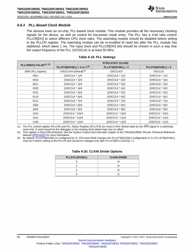
TMS320F28055, TMS320F28054, TMS320F28053TMS320F28052, TMS320F28051, TMS320F28050SPRS797B –NOVEMBER 2012–REVISED JULY 2014 www.ti.com
6.6.3 PLL-Based Clock ModuleThe devices have an on-chip, PLL-based clock module. This module provides all the necessary clockingsignals for the device, as well as control for low-power mode entry. The PLL has a 4-bit ratio controlPLLCR[DIV] to select different CPU clock rates. The watchdog module should be disabled before writingto the PLLCR register. The watchdog module can be re-enabled (if need be) after the PLL module hasstabilized, which takes 1 ms. The input clock and PLLCR[DIV] bits should be chosen in such a way thatthe output frequency of the PLL (VCOCLK) is at least 50 MHz.
Table 6-19. PLL Settings
SYSCLKOUT (CLKIN)PLLCR[DIV] VALUE (1) (2)
PLLSTS[DIVSEL] = 0 or 1 (3) PLLSTS[DIVSEL] = 2 PLLSTS[DIVSEL] = 30000 (PLL bypass) OSCCLK/4 (Default) (1) OSCCLK/2 OSCCLK
0001 (OSCCLK * 1)/4 (OSCCLK * 1)/2 (OSCCLK * 1)/10010 (OSCCLK * 2)/4 (OSCCLK * 2)/2 (OSCCLK * 2)/10011 (OSCCLK * 3)/4 (OSCCLK * 3)/2 (OSCCLK * 3)/10100 (OSCCLK * 4)/4 (OSCCLK * 4)/2 (OSCCLK * 4)/10101 (OSCCLK * 5)/4 (OSCCLK * 5)/2 (OSCCLK * 5)/10110 (OSCCLK * 6)/4 (OSCCLK * 6)/2 (OSCCLK * 6)/10111 (OSCCLK * 7)/4 (OSCCLK * 7)/2 (OSCCLK * 7)/11000 (OSCCLK * 8)/4 (OSCCLK * 8)/2 (OSCCLK * 8)/11001 (OSCCLK * 9)/4 (OSCCLK * 9)/2 (OSCCLK * 9)/11010 (OSCCLK * 10)/4 (OSCCLK * 10)/2 (OSCCLK * 10)/11011 (OSCCLK * 11)/4 (OSCCLK * 11)/2 (OSCCLK * 11)/11100 (OSCCLK * 12)/4 (OSCCLK * 12)/2 (OSCCLK * 12)/1
(1) The PLL control register (PLLCR) and PLL Status Register (PLLSTS) are reset to their default state by the XRS signal or a watchdogreset only. A reset issued by the debugger or the missing clock detect logic has no effect.
(2) This register is EALLOW protected. See the System Control and Interrupts chapter of the TMS320x2805x Piccolo Technical ReferenceManual (SPRUHE5) for more information.
(3) By default, PLLSTS[DIVSEL] is configured for /4. (The boot ROM changes the PLLSTS[DIVSEL] configuration to /1.) PLLSTS[DIVSEL]must be 0 before writing to the PLLCR and should be changed only after PLLSTS[PLLLOCKS] = 1.
Table 6-20. CLKIN Divide Options
PLLSTS [DIVSEL] CLKIN DIVIDE0 /41 /42 /23 /1
64 Detailed Description Copyright © 2012–2014, Texas Instruments IncorporatedSubmit Documentation Feedback
Product Folder Links: TMS320F28055 TMS320F28054 TMS320F28053 TMS320F28052 TMS320F28051TMS320F28050
TMS320F28055, TMS320F28054, TMS320F28053TMS320F28052, TMS320F28051, TMS320F28050
www.ti.com SPRS797B –NOVEMBER 2012–REVISED JULY 2014
The PLL-based clock module provides four modes of operation:• INTOSC1 (Internal Zero-pin Oscillator 1): INTOSC1 is the on-chip internal oscillator 1. INTOSC1 can
provide the clock for the Watchdog block, core and CPU-Timer 2.• INTOSC2 (Internal Zero-pin Oscillator 2): INTOSC2 is the on-chip internal oscillator 2. INTOSC2 can
provide the clock for the Watchdog block, core and CPU-Timer 2. Both INTOSC1 and INTOSC2 canbe independently chosen for the Watchdog block, core and CPU-Timer 2.
• Crystal/Resonator Operation: The on-chip (crystal) oscillator enables the use of an externalcrystal/resonator attached to the device to provide the time base. The crystal/resonator is connected tothe X1/X2 pins. Some devices may not have the X1/X2 pins. See Table 4-1 for details.
• External Clock Source Operation: If the on-chip (crystal) oscillator is not used, this mode allows theon-chip (crystal) oscillator to be bypassed. The device clocks are generated from an external clocksource input on the XCLKIN pin. Note that the XCLKIN is multiplexed with GPIO19 or GPIO38 pin. TheXCLKIN input can be selected as GPIO19 or GPIO38 via the XCLKINSEL bit in XCLK register. TheCLKCTL[XCLKINOFF] bit disables this clock input (forced low). If the clock source is not used or therespective pins are used as GPIOs, the user should disable at boot time.
Before changing clock sources, ensure that the target clock is present. If a clock is not present, then thatclock source must be disabled (using the CLKCTL register) before switching clocks.
Table 6-21. Possible PLL Configuration Modes
CLKIN ANDPLL MODE REMARKS PLLSTS[DIVSEL] SYSCLKOUTInvoked by the user setting the PLLOFF bit in the PLLSTS register. The PLL 0, 1 OSCCLK/4block is disabled in this mode. The PLL block being disabled can be useful in 2 OSCCLK/2PLL Off reducing system noise and for low-power operation. The PLLCR register mustfirst be set to 0x0000 (PLL Bypass) before entering this mode. The CPU clock 3 OSCCLK/1(CLKIN) is derived directly from the input clock on either X1/X2, X1 or XCLKIN.PLL Bypass is the default PLL configuration upon power-up or after an external 0, 1 OSCCLK/4reset (XRS). This mode is selected when the PLLCR register is set to 0x0000 or 2 OSCCLK/2PLL Bypass while the PLL locks to a new frequency after the PLLCR register has been
3 OSCCLK/1modified. In this mode, the PLL itself is bypassed but the PLL is not turned off.0, 1 OSCCLK * n/4
Achieved by writing a non-zero value n into the PLLCR register. Upon writing toPLL Enable 2 OSCCLK * n/2the PLLCR the device will switch to PLL Bypass mode until the PLL locks.3 OSCCLK * n/1
6.6.4 Loss of Input Clock (NMI Watchdog Function)The 2805x devices may be clocked from either one of the internal zero-pin oscillators (INTOSC1 orINTOSC2), the on-chip crystal oscillator, or from an external clock input. Regardless of the clock source,in PLL-enabled and PLL-bypass mode, if the input clock to the PLL vanishes, the PLL will issue a limp-mode clock at its output. This limp-mode clock continues to clock the CPU and peripherals at a typicalfrequency of 1–5 MHz.
When the limp mode is activated, a CLOCKFAIL signal is generated that is latched as an NMI interrupt.Depending on how the NMIRESETSEL bit has been configured, a reset to the device can be firedimmediately or the NMI watchdog counter can issue a reset when the counter overflows. In addition to thisaction, the Missing Clock Status (MCLKSTS) bit is set. The NMI interrupt could be used by the applicationto detect the input clock failure and initiate necessary corrective action such as switching over to analternative clock source (if available) or initiate a shut-down procedure for the system.
If the software does not respond to the clock-fail condition, the NMI watchdog triggers a reset after apreprogrammed time interval. Figure 6-10 shows the interrupt mechanisms involved.
Copyright © 2012–2014, Texas Instruments Incorporated Detailed Description 65Submit Documentation Feedback
Product Folder Links: TMS320F28055 TMS320F28054 TMS320F28053 TMS320F28052 TMS320F28051TMS320F28050

NMIFLG[NMINT]
1
0
GenerateInterrupt
PulseWhen
Input = 1
NMINT
Latch
Clear
Set Clear
NMIFLGCLR[NMINT]
XRS
0
NMICFG[CLOCKFAIL]
Latch
Clear
SetClear
XRS
NMIFLG[CLOCKFAIL]
NMI Watchdog
SYSCLKOUT
SYSRS
NMIRSNMIWDPRD[15:0]
NMIWDCNT[15:0]
NMIFLGCLR[CLOCKFAIL]
SYNC?
NMIFLGFRC[CLOCKFAIL]
SYSCLKOUT
See SystemControl Section
CLOCKFAIL
TMS320F28055, TMS320F28054, TMS320F28053TMS320F28052, TMS320F28051, TMS320F28050SPRS797B –NOVEMBER 2012–REVISED JULY 2014 www.ti.com
Figure 6-10. NMI-watchdog
6.6.5 CPU-Watchdog ModuleThe CPU-watchdog module on the 2805x device is similar to the one used on the 281x, 280x, and 283xxdevices. This module generates an output pulse, 512 oscillator clocks wide (OSCCLK), whenever the 8-bitwatchdog up counter has reached its maximum value. To prevent this occurrence, the user must disablethe counter or the software must periodically write a 0x55 + 0xAA sequence into the watchdog key registerthat resets the watchdog counter. Figure 6-11 shows the various functional blocks within the watchdogmodule.
Normally, when the input clocks are present, the CPU-watchdog counter decrements to initiate a CPU-watchdog reset or WDINT interrupt. However, when the external input clock fails, the CPU-watchdogcounter stops decrementing (that is, the watchdog counter does not change with the limp-mode clock).
NOTEThe CPU-watchdog is different from the NMI watchdog. The CPU-watchdog is the legacywatchdog that is present in all 28x devices.
NOTEApplications in which the correct CPU operating frequency is absolutely critical shouldimplement a mechanism by which the MCU will be held in reset, should the input clocks everfail. For example, an R-C circuit may be used to trigger the XRS pin of the MCU, should thecapacitor ever get fully charged. An I/O pin may be used to discharge the capacitor on aperiodic basis to prevent the capacitor from getting fully charged. Such a circuit would alsohelp in detecting failure of the flash memory.
66 Detailed Description Copyright © 2012–2014, Texas Instruments IncorporatedSubmit Documentation Feedback
Product Folder Links: TMS320F28055 TMS320F28054 TMS320F28053 TMS320F28052 TMS320F28051TMS320F28050

/512WDCLK
WDCR (WDPS[2:0])
WDCLK
WDCNTR(7:0)
WDKEY(7:0)
Good K ey
1 0 1
WDCR (WDCHK[2:0])
Bad
WDCHK
Key
WDCR (WDDIS)
Clear Counter
SCSR (WDENINT)
Watchdog
Prescaler
Generate
Output Pulse
(512 OSCCLKs)
8-Bit
Watchdog
Counter
CLR
WDRST
WDINTWatchdog
55 + AA
Key Detector
Core-reset
XRS
WDRST(A)
Internal
Pullup
TMS320F28055, TMS320F28054, TMS320F28053TMS320F28052, TMS320F28051, TMS320F28050
www.ti.com SPRS797B –NOVEMBER 2012–REVISED JULY 2014
A. The WDRST signal is driven low for 512 OSCCLK cycles.
Figure 6-11. CPU-watchdog Module
The WDINT signal enables the watchdog to be used as a wakeup from IDLE/STANDBY mode.
In STANDBY mode, all peripherals are turned off on the device. The only peripheral that remainsfunctional is the CPU-watchdog. This module will run off OSCCLK. The WDINT signal is fed to the LPMblock so that the signal can wake the device from STANDBY (if enabled). See Section 6.7, Low-powerModes Block, for more details.
In IDLE mode, the WDINT signal can generate an interrupt to the CPU, via the PIE, to take the CPU out ofIDLE mode.
In HALT mode, the CPU-watchdog can be used to wake up the device through a device reset.
Copyright © 2012–2014, Texas Instruments Incorporated Detailed Description 67Submit Documentation Feedback
Product Folder Links: TMS320F28055 TMS320F28054 TMS320F28053 TMS320F28052 TMS320F28051TMS320F28050

TMS320F28055, TMS320F28054, TMS320F28053TMS320F28052, TMS320F28051, TMS320F28050SPRS797B –NOVEMBER 2012–REVISED JULY 2014 www.ti.com
6.7 Low-power Modes BlockTable 6-22 summarizes the various modes.
Table 6-22. Low-power Modes
MODE LPMCR0(1:0) OSCCLK CLKIN SYSCLKOUT EXIT (1)
XRS, CPU-watchdog interrupt, anyIDLE 00 On On On enabled interruptOn XRS, CPU-watchdog interrupt, GPIOSTANDBY 01 Off Off(CPU-watchdog still running) Port A signal, debugger (2)
Off(on-chip crystal oscillator and XRS, GPIO Port A signal, debugger (2),HALT (3) 1X PLL turned off, zero-pin oscillator Off Off CPU-watchdogand CPU-watchdog state
dependent on user code.)
(1) The Exit column lists which signals or under what conditions the low power mode is exited. A low signal, on any of the signals, exits thelow power condition. This signal must be kept low long enough for an interrupt to be recognized by the device. Otherwise, the low-powermode will not be exited and the device will go back into the indicated low power mode.
(2) The JTAG port can still function even if the CPU clock (CLKIN) is turned off.(3) The WDCLK must be active for the device to go into HALT mode.
The various low-power modes operate as follows:
IDLE Mode: This mode is exited by any enabled interrupt that is recognized by theprocessor. The LPM block performs no tasks during this mode as long asthe LPMCR0(LPM) bits are set to 0,0.
STANDBY Mode: Any GPIO port A signal (GPIO[31:0]) can wake the device from STANDBYmode. The user must select which signals will wake the device in theGPIOLPMSEL register. The selected signals are also qualified by theOSCCLK before waking the device. The number of OSCCLKs is specified inthe LPMCR0 register.
HALT Mode: CPU-watchdog, XRS, and any GPIO port A signal (GPIO[31:0]) can wakethe device from HALT mode. The user selects the signal in theGPIOLPMSEL register.
NOTEThe low-power modes do not affect the state of the output pins (PWM pins included). Theywill be in whatever state the code left them in when the IDLE instruction was executed. Seethe System Control and Interrupts chapter of the TMS320x2805x Piccolo TechnicalReference Manual (SPRUHE5) for more details.
68 Detailed Description Copyright © 2012–2014, Texas Instruments IncorporatedSubmit Documentation Feedback
Product Folder Links: TMS320F28055 TMS320F28054 TMS320F28053 TMS320F28052 TMS320F28051TMS320F28050

CPU TIMER 2
CPU TIMER 0
Watchdog
Peripherals
(SPI, SCI, ePWM, I C, eCAP, ADC, eQEP, CLA, eCAN)2
TINT0
XINT1Interrupt Control
XINT1
XINT1CR(15:0)
Interrupt ControlXINT2
XINT2CR(15:0)
GPIOMUX
WDINT
INT1to
INT12
NMI
XINT2CTR(15:0)
XINT3CTR(15:0)
CPU TIMER 1TINT2
Low Power ModesLPMINT
WAKEINTSync
SYSCLKOUT
MU
X
XINT2
XINT3
ADCXINT2SOC
GPIOXINT1SEL(4:0)
GPIOXINT2SEL(4:0)
GPIOXINT3SEL(4:0)
Interrupt ControlXINT3
XINT3CR(15:0)
XINT3CTR(15:0)
NMI interrupt with watchdog function(See the NMI Watchdog section.) NMIRS
System Control(See the SystemControl section.)
INT14
INT13
GPIO0.int
GPIO31.int
CLOCKFAIL
CPUTMR2CLK
C28Core
MU
XM
UX
TINT1
PIE
Up
to
96 In
terr
up
ts
TMS320F28055, TMS320F28054, TMS320F28053TMS320F28052, TMS320F28051, TMS320F28050
www.ti.com SPRS797B –NOVEMBER 2012–REVISED JULY 2014
6.8 InterruptsFigure 6-12 shows how the various interrupt sources are multiplexed.
Figure 6-12. External and PIE Interrupt Sources
Copyright © 2012–2014, Texas Instruments Incorporated Detailed Description 69Submit Documentation Feedback
Product Folder Links: TMS320F28055 TMS320F28054 TMS320F28053 TMS320F28052 TMS320F28051TMS320F28050

INT12
MUX
INT11
INT2
INT1
CPU
(Enable)(Flag)
INTx
INTx.8
PIEIERx[8:1] PIEIFRx[8:1]
MUX
INTx.7
INTx.6
INTx.5
INTx.4
INTx.3
INTx.2
INTx.1
FromPeripherals
orExternal
Interrupts
(Enable) (Flag)
IER[12:1]IFR[12:1]
GlobalEnable
INTM
1
0
PIEACKx
(Enable/Flag)
TMS320F28055, TMS320F28054, TMS320F28053TMS320F28052, TMS320F28051, TMS320F28050SPRS797B –NOVEMBER 2012–REVISED JULY 2014 www.ti.com
Eight PIE block interrupts are grouped into one CPU interrupt. In total, 12 CPU interrupt groups, with8 interrupts per group equals 96 possible interrupts. Table 6-23 shows the interrupts used by 2805xdevices.
The TRAP #VectorNumber instruction transfers program control to the interrupt service routinecorresponding to the vector specified. TRAP #0 attempts to transfer program control to the addresspointed to by the reset vector. The PIE vector table does not, however, include a reset vector. Therefore,TRAP #0 should not be used when the PIE is enabled. Doing so will result in undefined behavior.
When the PIE is enabled, TRAP #1 through TRAP #12 will transfer program control to the interrupt serviceroutine corresponding to the first vector within the PIE group. For example: TRAP #1 fetches the vectorfrom INT1.1, TRAP #2 fetches the vector from INT2.1, and so forth.
Figure 6-13. Multiplexing of Interrupts Using the PIE Block
70 Detailed Description Copyright © 2012–2014, Texas Instruments IncorporatedSubmit Documentation Feedback
Product Folder Links: TMS320F28055 TMS320F28054 TMS320F28053 TMS320F28052 TMS320F28051TMS320F28050

TMS320F28055, TMS320F28054, TMS320F28053TMS320F28052, TMS320F28051, TMS320F28050
www.ti.com SPRS797B –NOVEMBER 2012–REVISED JULY 2014
Table 6-23. PIE MUXed Peripheral Interrupt Vector Table (1)
INTx.8 INTx.7 INTx.6 INTx.5 INTx.4 INTx.3 INTx.2 INTx.1
INT1.y WAKEINT TINT0 ADCINT9 XINT2 XINT1 Reserved ADCINT2 ADCINT1
(LPM/WD) (TIMER 0) (ADC) Ext. int. 2 Ext. int. 1 – (ADC) (ADC)
0xD4E 0xD4C 0xD4A 0xD48 0xD46 0xD44 0xD42 0xD40
INT2.y Reserved EPWM7_TZINT EPWM6_TZINT EPWM5_TZINT EPWM4_TZINT EPWM3_TZINT EPWM2_TZINT EPWM1_TZINT
– (ePWM7) (ePWM6) (ePWM5) (ePWM4) (ePWM3) (ePWM2) (ePWM1)
0xD5E 0xD5C 0xD5A 0xD58 0xD56 0xD54 0xD52 0xD50
INT3.y Reserved EPWM7_INT EPWM6_INT EPWM5_INT EPWM4_INT EPWM3_INT EPWM2_INT EPWM1_INT
– (ePWM7) (ePWM6) (ePWM5) (ePWM4) (ePWM3) (ePWM2) (ePWM1)
0xD6E 0xD6C 0xD6A 0xD68 0xD66 0xD64 0xD62 0xD60
INT4.y Reserved Reserved Reserved Reserved Reserved Reserved Reserved ECAP1_INT
– – – – – – – (eCAP1)
0xD7E 0xD7C 0xD7A 0xD78 0xD76 0xD74 0xD72 0xD70
INT5.y Reserved Reserved Reserved Reserved Reserved Reserved Reserved EQEP1_INT
– – – – – – – (eQEP1)
0xD8E 0xD8C 0xD8A 0xD88 0xD86 0xD84 0xD82 0xD80
INT6.y Reserved Reserved Reserved Reserved Reserved Reserved SPITXINTA SPIRXINTA
– – – – – – (SPI-A) (SPI-A)
0xD9E 0xD9C 0xD9A 0xD98 0xD96 0xD94 0xD92 0xD90
INT7.y Reserved Reserved Reserved Reserved Reserved Reserved Reserved Reserved
– – – – – – – –
0xDAE 0xDAC 0xDAA 0xDA8 0xDA6 0xDA4 0xDA2 0xDA0
INT8.y Reserved Reserved SCITXINTC SCIRXINTC Reserved Reserved I2CINT2A I2CINT1A
– – (SCI-C) (SCI-C) – – (I2C-A) (I2C-A)
0xDBE 0xDBC 0xDBA 0xDB8 0xDB6 0xDB4 0xDB2 0xDB0
INT9.y Reserved Reserved ECAN1_INTA ECAN0_INTA SCITXINTB SCIRXINTB SCITXINTA SCIRXINTA
– – (CAN-A) (CAN-A) (SCI-B) (SCI-B) (SCI-A) (SCI-A)
0xDCE 0xDCC 0xDCA 0xDC8 0xDC6 0xDC4 0xDC2 0xDC0
INT10.y ADCINT8 ADCINT7 ADCINT6 ADCINT5 ADCINT4 ADCINT3 ADCINT2 ADCINT1
(ADC) (ADC) (ADC) (ADC) (ADC) (ADC) (ADC) (ADC)
(ePWM16) (ePWM15) (ePWM14) (ePWM13) (ePWM12) (ePWM11) (ePWM10) (ePWM9)
0xDDE 0xDDC 0xDDA 0xDD8 0xDD6 0xDD4 0xDD2 0xDD0
INT11.y CLA1_INT8 CLA1_INT7 CLA1_INT6 CLA1_INT5 CLA1_INT4 CLA1_INT3 CLA1_INT2 CLA1_INT1
(CLA) (CLA) (CLA) (CLA) (CLA) (CLA) (CLA) (CLA)
(ePWM16) (ePWM15) (ePWM14) (ePWM13) (ePWM12) (ePWM11) (ePWM10) (ePWM9)
0xDEE 0xDEC 0xDEA 0xDE8 0xDE6 0xDE4 0xDE2 0xDE0
INT12.y LUF LVF Reserved Reserved Reserved Reserved Reserved XINT3
(CLA) (CLA) – – – – – Ext. Int. 3
0xDFE 0xDFC 0xDFA 0xDF8 0xDF6 0xDF4 0xDF2 0xDF0
(1) Out of 96 possible interrupts, some interrupts are not used. These interrupts are reserved for future devices. These interrupts can beused as software interrupts if they are enabled at the PIEIFRx level, provided none of the interrupts within the group is being used by aperipheral. Otherwise, interrupts coming in from peripherals may be lost by accidentally clearing their flag while modifying the PIEIFR.To summarize, there are two safe cases when the reserved interrupts could be used as software interrupts:• No peripheral within the group is asserting interrupts.• No peripheral interrupts are assigned to the group (for example, PIE group 7).
Copyright © 2012–2014, Texas Instruments Incorporated Detailed Description 71Submit Documentation Feedback
Product Folder Links: TMS320F28055 TMS320F28054 TMS320F28053 TMS320F28052 TMS320F28051TMS320F28050

TMS320F28055, TMS320F28054, TMS320F28053TMS320F28052, TMS320F28051, TMS320F28050SPRS797B –NOVEMBER 2012–REVISED JULY 2014 www.ti.com
Table 6-24. PIE Configuration and Control Registers
NAME ADDRESS SIZE (x16) DESCRIPTION (1)
PIECTRL 0x0CE0 1 PIE, Control RegisterPIEACK 0x0CE1 1 PIE, Acknowledge RegisterPIEIER1 0x0CE2 1 PIE, INT1 Group Enable RegisterPIEIFR1 0x0CE3 1 PIE, INT1 Group Flag RegisterPIEIER2 0x0CE4 1 PIE, INT2 Group Enable RegisterPIEIFR2 0x0CE5 1 PIE, INT2 Group Flag RegisterPIEIER3 0x0CE6 1 PIE, INT3 Group Enable RegisterPIEIFR3 0x0CE7 1 PIE, INT3 Group Flag RegisterPIEIER4 0x0CE8 1 PIE, INT4 Group Enable RegisterPIEIFR4 0x0CE9 1 PIE, INT4 Group Flag RegisterPIEIER5 0x0CEA 1 PIE, INT5 Group Enable RegisterPIEIFR5 0x0CEB 1 PIE, INT5 Group Flag RegisterPIEIER6 0x0CEC 1 PIE, INT6 Group Enable RegisterPIEIFR6 0x0CED 1 PIE, INT6 Group Flag RegisterPIEIER7 0x0CEE 1 PIE, INT7 Group Enable RegisterPIEIFR7 0x0CEF 1 PIE, INT7 Group Flag RegisterPIEIER8 0x0CF0 1 PIE, INT8 Group Enable RegisterPIEIFR8 0x0CF1 1 PIE, INT8 Group Flag RegisterPIEIER9 0x0CF2 1 PIE, INT9 Group Enable RegisterPIEIFR9 0x0CF3 1 PIE, INT9 Group Flag RegisterPIEIER10 0x0CF4 1 PIE, INT10 Group Enable RegisterPIEIFR10 0x0CF5 1 PIE, INT10 Group Flag RegisterPIEIER11 0x0CF6 1 PIE, INT11 Group Enable RegisterPIEIFR11 0x0CF7 1 PIE, INT11 Group Flag RegisterPIEIER12 0x0CF8 1 PIE, INT12 Group Enable RegisterPIEIFR12 0x0CF9 1 PIE, INT12 Group Flag RegisterReserved 0x0CFA – 6 Reserved
0x0CFF
(1) The PIE configuration and control registers are not protected by EALLOW mode. The PIE vector tableis protected.
72 Detailed Description Copyright © 2012–2014, Texas Instruments IncorporatedSubmit Documentation Feedback
Product Folder Links: TMS320F28055 TMS320F28054 TMS320F28053 TMS320F28052 TMS320F28051TMS320F28050

XINT1, XINT2, XINT3
tw(INT)
Interrupt Vector
td(INT)
Address bus(internal)
TMS320F28055, TMS320F28054, TMS320F28053TMS320F28052, TMS320F28051, TMS320F28050
www.ti.com SPRS797B –NOVEMBER 2012–REVISED JULY 2014
6.8.1 External Interrupts
Table 6-25. External Interrupt Registers
NAME ADDRESS SIZE (x16) DESCRIPTIONXINT1CR 0x00 7070 1 XINT1 configuration registerXINT2CR 0x00 7071 1 XINT2 configuration registerXINT3CR 0x00 7072 1 XINT3 configuration registerXINT1CTR 0x00 7078 1 XINT1 counter registerXINT2CTR 0x00 7079 1 XINT2 counter registerXINT3CTR 0x00 707A 1 XINT3 counter register
Each external interrupt can be enabled, disabled, or qualified using positive, negative, or both positive andnegative edge. For more information, see the System Control and Interrupts chapter of theTMS320x2805x Piccolo Technical Reference Manual (SPRUHE5).
6.8.1.1 External Interrupt Electrical Data/Timing
Table 6-26. External Interrupt Timing Requirements (1)
TEST CONDITIONS MIN MAX UNITSynchronous 1tc(SCO) cycles
tw(INT)(2) Pulse duration, INT input low/high
With qualifier 1tc(SCO) + tw(IQSW) cycles
(1) For an explanation of the input qualifier parameters, see Table 6-72.(2) This timing is applicable to any GPIO pin configured for ADCSOC functionality.
Table 6-27. External Interrupt Switching Characteristics (1)
over recommended operating conditions (unless otherwise noted)PARAMETER MIN MAX UNIT
td(INT) Delay time, INT low/high to interrupt-vector fetch tw(IQSW) + 12tc(SCO) cycles
(1) For an explanation of the input qualifier parameters, see Table 6-72.
Figure 6-14. External Interrupt Timing
Copyright © 2012–2014, Texas Instruments Incorporated Detailed Description 73Submit Documentation Feedback
Product Folder Links: TMS320F28055 TMS320F28054 TMS320F28053 TMS320F28052 TMS320F28051TMS320F28050

TMS320F28055, TMS320F28054, TMS320F28053TMS320F28052, TMS320F28051, TMS320F28050SPRS797B –NOVEMBER 2012–REVISED JULY 2014 www.ti.com
6.9 Peripherals
6.9.1 Control Law Accelerator
6.9.1.1 CLA Device-Specific Information
The CLA extends the capabilities of the C28x CPU by adding parallel processing. Time-critical controlloops serviced by the CLA can achieve low ADC sample to output delay. Thus, the CLA enables fastersystem response and higher frequency control loops. Utilizing the CLA for time-critical tasks frees up themain CPU to perform other system and communication functions concurently. The following is a list ofmajor features of the CLA.• Clocked at the same rate as the main CPU (SYSCLKOUT).• An independent architecture allowing CLA algorithm execution independent of the main C28x CPU.
– Complete bus architecture:• Program address bus and program data bus• Data address bus, data read bus, and data write bus
– Independent eight-stage pipeline.– 12-bit program counter (MPC)– Four 32-bit result registers (MR0–MR3)– Two 16-bit auxillary registers (MAR0, MAR1)– Status register (MSTF)
• Instruction set includes:– IEEE single-precision (32-bit) floating-point math operations– Floating-point math with parallel load or store– Floating-point multiply with parallel add or subtract– 1/X and 1/sqrt(X) estimations– Data type conversions.– Conditional branch and call– Data load and store operations
• The CLA program code can consist of up to eight tasks or interrupt service routines.– The start address of each task is specified by the MVECT registers.– No limit on task size as long as the tasks fit within the CLA program memory space.– One task is serviced at a time through to completion. There is no nesting of tasks.– Upon task completion, a task-specific interrupt is flagged within the PIE.– When a task finishes, the next highest-priority pending task is automatically started.
• Task trigger mechanisms:– C28x CPU via the IACK instruction– Task1 to Task7: the corresponding ADC, ePWM, eQEP, or eCAP module interrupt. For example:
• Task1: ADCINT1 or EPWM1_INT• Task2: ADCINT2 or EPWM2_INT• Task4: ADCINT4 or EPWM4_INT or EQEPx_INT or ECAPx_INT• Task7: ADCINT7 or EPWM7_INT or EQEPx_INT or ECAPx_INT
– Task8: ADCINT8 or by CPU Timer 0 or EQEPx_INT or ECAPx_INT• Memory and Shared Peripherals:
– Two dedicated message RAMs for communication between the CLA and the main CPU.– The C28x CPU can map CLA program and data memory to the main CPU space or CLA space.– The CLA has direct access to the CLA Data ROM that stores the math tables required by the
routines in the CLA Math Library.– The CLA has direct access to the ADC Result registers, comparator and DAC registers, eCAP,
eQEP, and ePWM registers.74 Detailed Description Copyright © 2012–2014, Texas Instruments Incorporated
Submit Documentation FeedbackProduct Folder Links: TMS320F28055 TMS320F28054 TMS320F28053 TMS320F28052 TMS320F28051
TMS320F28050

CLA_INT1 to CLA_INT8
MVECT1
MIFR
MIERMIFRC
MVECT2
MIRUN
MPERINT1
to
MPERINT8
PIEMain28xCPU
CLA
Program
Memory
MMEMCFG
MIOVFMICLR
MCTL
MICLROVF
MPISRCSEL1
MVECT3MVECT4MVECT5MVECT6MVECT7MVECT8
PU
BU
S
INT11
INT12
Peripheral Interrupts
ADCINT1 to ADCINT8
EPWM1_INT to EPWM7_INT
ECAP1_INT
EQEP1_INT
CPU Timer 0
Map to CLA orCPU Space
Main CPU Read/Write Data Bus
CLA Program Address Bus
CLA Program Data Bus
Map to CLA orCPU Space
CLAData
Memory
CLADataROM
Comparator+ DAC
Registers
ePWMRegisters
eCAPRegisters
eQEPRegisters
ADCResult
Registers
CLAShared
MessageRAMs
Main
CP
U B
us
MR0(32)
MPC(12)
MR1(32)
MR3(32)MAR0(32)
MSTF(32)
MR2(32)
MAR1(32)
CLA Data Read Address Bus
CLA Data Write Data Bus
CLA Data Write Address Bus
CLA Data Read Data Bus
MEALLOW
Main CPU Read Data Bus
CLA ExecutionRegisters
CLA ControlRegisters
SYSCLKOUTCLAENCLK
SYSRS
LVFLUF
IACK
CL
AD
ata
Bu
s
TMS320F28055, TMS320F28054, TMS320F28053TMS320F28052, TMS320F28051, TMS320F28050
www.ti.com SPRS797B –NOVEMBER 2012–REVISED JULY 2014
Figure 6-15. CLA Block Diagram
Copyright © 2012–2014, Texas Instruments Incorporated Detailed Description 75Submit Documentation Feedback
Product Folder Links: TMS320F28055 TMS320F28054 TMS320F28053 TMS320F28052 TMS320F28051TMS320F28050
TMS320F28055, TMS320F28054, TMS320F28053TMS320F28052, TMS320F28051, TMS320F28050SPRS797B –NOVEMBER 2012–REVISED JULY 2014 www.ti.com
6.9.1.2 CLA Register Descriptions
Table 6-28. CLA Control Registers
CLA1 EALLOWREGISTER NAME SIZE (x16) DESCRIPTION (1)ADDRESS PROTECTED
MVECT1 0x1400 1 Yes CLA Interrupt/Task 1 Start AddressMVECT2 0x1401 1 Yes CLA Interrupt/Task 2 Start AddressMVECT3 0x1402 1 Yes CLA Interrupt/Task 3 Start AddressMVECT4 0x1403 1 Yes CLA Interrupt/Task 4 Start AddressMVECT5 0x1404 1 Yes CLA Interrupt/Task 5 Start AddressMVECT6 0x1405 1 Yes CLA Interrupt/Task 6 Start AddressMVECT7 0x1406 1 Yes CLA Interrupt/Task 7 Start AddressMVECT8 0x1407 1 Yes CLA Interrupt/Task 8 Start Address
MCTL 0x1410 1 Yes CLA Control RegisterMMEMCFG 0x1411 1 Yes CLA Memory Configure Register
MPISRCSEL1 0x1414 2 Yes Peripheral Interrupt Source Select Register 1MIFR 0x1420 1 Yes Interrupt Flag Register
MIOVF 0x1421 1 Yes Interrupt Overflow RegisterMIFRC 0x1422 1 Yes Interrupt Force RegisterMICLR 0x1423 1 Yes Interrupt Clear Register
MICLROVF 0x1424 1 Yes Interrupt Overflow Clear RegisterMIER 0x1425 1 Yes Interrupt Enable Register
MIRUN 0x1426 1 Yes Interrupt RUN RegisterMPC (2) 0x1428 1 – CLA Program CounterMAR0 (2) 0x142A 1 – CLA Aux Register 0MAR1 (2) 0x142B 1 – CLA Aux Register 1MSTF (2) 0x142E 2 – CLA STF RegisterMR0 (2) 0x1430 2 – CLA R0H RegisterMR1 (2) 0x1434 2 – CLA R1H RegisterMR2 (2) 0x1438 2 – CLA R2H RegisterMR3 (2) 0x143C 2 – CLA R3H Register
(1) All registers in this table are DCSM protected(2) The main C28x CPU has read only access to this register for debug purposes. The main CPU cannot perform CPU or debugger writes
to this register.
Table 6-29. CLA Message RAM
ADDRESS RANGE SIZE (x16) DESCRIPTION0x1480 – 0x14FF 128 CLA to CPU Message RAM0x1500 – 0x157F 128 CPU to CLA Message RAM
76 Detailed Description Copyright © 2012–2014, Texas Instruments IncorporatedSubmit Documentation Feedback
Product Folder Links: TMS320F28055 TMS320F28054 TMS320F28053 TMS320F28052 TMS320F28051TMS320F28050

0,ValueDigital = V0inputwhen £
VV
VVoltageAnalogInput4096ValueDigital
REFLOREFHI
REFLO
-
-´= VinputV0when REFHI<<
4095,ValueDigital = Vinputwhen REFHI³
0,ValueDigital = V0inputwhen £
3.3
VVoltageAnalogInput4096ValueDigital REFLO-
´= V3.3inputV0when <<
4095,ValueDigital = V3.3inputwhen ³
TMS320F28055, TMS320F28054, TMS320F28053TMS320F28052, TMS320F28051, TMS320F28050
www.ti.com SPRS797B –NOVEMBER 2012–REVISED JULY 2014
6.9.2 Analog Block
6.9.2.1 Analog-to-Digital Converter
6.9.2.1.1 ADC Device-Specific Information
The core of the ADC contains a single 12-bit converter fed by two sample-and-hold circuits. The sample-and-hold circuits can be sampled simultaneously or sequentially. These, in turn, are fed by a total of up to16 analog input channels. The converter can be configured to run with an internal bandgap reference tocreate true-voltage based conversions or with a pair of external voltage references (VREFHI/VREFLO) tocreate ratiometric-based conversions.
Contrary to previous ADC types, this ADC is not sequencer-based. The user can easily create a series ofconversions from a single trigger. However, the basic principle of operation is centered around theconfigurations of individual conversions, called SOCs, or Start-Of-Conversions.
Functions of the ADC module include:• 12-bit ADC core with built-in dual sample-and-hold (S/H)• Simultaneous sampling or sequential sampling modes• Full range analog input: 0 V to 3.3 V fixed, or VREFHI/VREFLO ratiometric. The digital value of the input
analog voltage is derived by:– Internal Reference (VREFLO = VSSA. VREFHI must not exceed VDDA when using either internal or
external reference modes.)
– External Reference (VREFHI/VREFLO connected to external references. VREFHI must not exceed VDDAwhen using either internal or external reference modes.)
• Up to 16-channel, multiplexed inputs• 16 SOCs, configurable for trigger, sample window, and channel• 16 result registers (individually addressable) to store conversion values• Multiple trigger sources
– S/W – software immediate start– ePWM 1–7– GPIO XINT2– CPU Timer 0, CPU Timer 1, CPU Timer 2– ADCINT1, ADCINT2
• 9 flexible PIE interrupts, can configure interrupt request after any conversion
Copyright © 2012–2014, Texas Instruments Incorporated Detailed Description 77Submit Documentation Feedback
Product Folder Links: TMS320F28055 TMS320F28054 TMS320F28053 TMS320F28052 TMS320F28051TMS320F28050
TMS320F28055, TMS320F28054, TMS320F28053TMS320F28052, TMS320F28051, TMS320F28050SPRS797B –NOVEMBER 2012–REVISED JULY 2014 www.ti.com
Table 6-30. ADC Configuration and Control Registers
SIZE EALLOWREGISTER NAME ADDRESS DESCRIPTION(x16) PROTECTEDADCCTL1 0x7100 1 Yes Control 1 RegisterADCCTL2 0x7101 1 Yes Control 2 RegisterADCINTFLG 0x7104 1 No Interrupt Flag RegisterADCINTFLGCLR 0x7105 1 No Interrupt Flag Clear RegisterADCINTOVF 0x7106 1 No Interrupt Overflow RegisterADCINTOVFCLR 0x7107 1 No Interrupt Overflow Clear RegisterINTSEL1N2 0x7108 1 Yes Interrupt 1 and 2 Selection RegisterINTSEL3N4 0x7109 1 Yes Interrupt 3 and 4 Selection RegisterINTSEL5N6 0x710A 1 Yes Interrupt 5 and 6 Selection RegisterINTSEL7N8 0x710B 1 Yes Interrupt 7 and 8 Selection RegisterINTSEL9N10 0x710C 1 Yes Interrupt 9 Selection Register (reserved Interrupt 10 Selection)SOCPRICTL 0x7110 1 Yes SOC Priority Control RegisterADCSAMPLEMODE 0x7112 1 Yes Sampling Mode RegisterADCINTSOCSEL1 0x7114 1 Yes Interrupt SOC Selection 1 Register (for 8 channels)ADCINTSOCSEL2 0x7115 1 Yes Interrupt SOC Selection 2 Register (for 8 channels)ADCSOCFLG1 0x7118 1 No SOC Flag 1 Register (for 16 channels)ADCSOCFRC1 0x711A 1 No SOC Force 1 Register (for 16 channels)ADCSOCOVF1 0x711C 1 No SOC Overflow 1 Register (for 16 channels)ADCSOCOVFCLR1 0x711E 1 No SOC Overflow Clear 1 Register (for 16 channels)ADCSOC0CTL to 0x7120 – 1 Yes SOC0 Control Register to SOC15 Control RegisterADCSOC15CTL 0x712FADCREFTRIM 0x7140 1 Yes Reference Trim RegisterADCOFFTRIM 0x7141 1 Yes Offset Trim RegisterADCREV 0x714F 1 No Revision Register
Table 6-31. ADC Result Registers (Mapped to PF0)
SIZE EALLOWREGISTER NAME ADDRESS DESCRIPTION(x16) PROTECTEDADCRESULT0 to 0xB00 – 1 No ADC Result 0 Register to ADC Result 15 RegisterADCRESULT15 0xB0F
78 Detailed Description Copyright © 2012–2014, Texas Instruments IncorporatedSubmit Documentation Feedback
Product Folder Links: TMS320F28055 TMS320F28054 TMS320F28053 TMS320F28052 TMS320F28051TMS320F28050
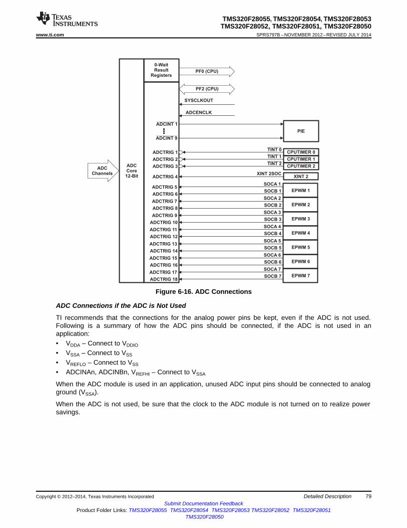
PF0 (CPU)
PF2 (CPU)
SYSCLKOUT
ADCENCLK
ADCChannels
ADCCore12-Bit
0-WaitResult
Registers
ADCINT 1
ADCINT 9
ADCTRIG 1TINT 0
PIE
CPUTIMER 0
ADCTRIG 2TINT 1
CPUTIMER 1
ADCTRIG 3TINT 2
CPUTIMER 2
ADCTRIG 4XINT 2SOC
XINT 2
ADCTRIG 5SOCA 1
EPWM 1ADCTRIG 6
SOCB 1
ADCTRIG 7SOCA 2
EPWM 2ADCTRIG 8
SOCB 2
ADCTRIG 9SOCA 3
EPWM 3ADCTRIG 10
SOCB 3
ADCTRIG 11SOCA 4
EPWM 4ADCTRIG 12
SOCB 4
ADCTRIG 13SOCA 5
EPWM 5ADCTRIG 14
SOCB 5
ADCTRIG 15SOCA 6
EPWM 6ADCTRIG 16
SOCB 6
ADCTRIG 17SOCA 7
EPWM 7ADCTRIG 18
SOCB 7
TMS320F28055, TMS320F28054, TMS320F28053TMS320F28052, TMS320F28051, TMS320F28050
www.ti.com SPRS797B –NOVEMBER 2012–REVISED JULY 2014
Figure 6-16. ADC Connections
ADC Connections if the ADC is Not Used
TI recommends that the connections for the analog power pins be kept, even if the ADC is not used.Following is a summary of how the ADC pins should be connected, if the ADC is not used in anapplication:• VDDA – Connect to VDDIO
• VSSA – Connect to VSS
• VREFLO – Connect to VSS
• ADCINAn, ADCINBn, VREFHI – Connect to VSSA
When the ADC module is used in an application, unused ADC input pins should be connected to analogground (VSSA).
When the ADC is not used, be sure that the clock to the ADC module is not turned on to realize powersavings.
Copyright © 2012–2014, Texas Instruments Incorporated Detailed Description 79Submit Documentation Feedback
Product Folder Links: TMS320F28055 TMS320F28054 TMS320F28053 TMS320F28052 TMS320F28051TMS320F28050

TMS320F28055, TMS320F28054, TMS320F28053TMS320F28052, TMS320F28051, TMS320F28050SPRS797B –NOVEMBER 2012–REVISED JULY 2014 www.ti.com
6.9.2.1.2 ADC Electrical Data/Timing
Table 6-32. ADC Electrical Characteristics
PARAMETER MIN TYP MAX UNITDC SPECIFICATIONSResolution 12 BitsADC clock 0.5 60 MHz
28055, 28054, 28053, 10 63 ADC28052Sample Window (see Table 6-33) Clocks28051, 28050 24 63
ACCURACYINL (Integral nonlinearity) (1) –4 4.5 LSBDNL (Differential nonlinearity), no missing codes –1 1.5 LSB
Executing a single self- –20 0 20recalibration (3)Offset error (2) LSB
Executing periodic self- –4 0 4recalibration (4)
Overall gain error with internal reference –60 60 LSBOverall gain error with external reference –40 40 LSBChannel-to-channel offset variation –4 4 LSBChannel-to-channel gain variation –4 4 LSBADC temperature coefficient with internal reference –50 ppm/°CADC temperature coefficient with external reference –20 ppm/°CVREFLO –100 µAVREFHI 100 µAANALOG INPUTAnalog input voltage with internal reference 0 3.3 VAnalog input voltage with external reference VREFLO VREFHI VVREFLO input voltage VSSA 0.66 V
2.64 VDDAVREFHI input voltage (5) Vwith VREFLO = VSSA 1.98 VDDA
Input capacitance 5 pFInput leakage current ±2 μA
(1) INL will degrade when the ADC input voltage goes above VDDA.(2) 1 LSB has the weighted value of full-scale range (FSR)/4096. FSR is 3.3 V with internal reference and VREFHI - VREFLO for external
reference.(3) For more details, see the TMS320F28055, TMS320F28054, TMS320F28053, TMS320F28052, TMS320F28051, TMS320F28050
Piccolo MCU Silicon Errata (SPRZ362).(4) Periodic self-recalibration will remove system-level and temperature dependencies on the ADC zero offset error. This can be performed
as needed in the application without sacrificing an ADC channel by using the procedure listed in the "ADC Zero Offset Calibration"section in the Analog-to-Digital Converter and Comparator chapter of the TMS320x2805x Piccolo Technical Reference Manual(SPRUHE5).
(5) VREFHI must not exceed VDDA when using either internal or external reference modes.
Table 6-33. ACQPS Values (1)
OVERLAP MODE NONOVERLAP MODENon-PGA 9, 10, 23, 36, 49, 62 15, 16, 28, 29, 41, 42, 54, 55PGA 23, 36, 49, 62 15, 16, 28, 29, 41, 42, 54, 55
(1) ACQPS = 6 can be used for the first sample if it is thrown away.
80 Detailed Description Copyright © 2012–2014, Texas Instruments IncorporatedSubmit Documentation Feedback
Product Folder Links: TMS320F28055 TMS320F28054 TMS320F28053 TMS320F28052 TMS320F28051TMS320F28050

ADCSOCAO
ADCSOCBOor
tw(ADCSOCL)
TMS320F28055, TMS320F28054, TMS320F28053TMS320F28052, TMS320F28051, TMS320F28050
www.ti.com SPRS797B –NOVEMBER 2012–REVISED JULY 2014
Table 6-34. ADC Power Modes
ADC OPERATING MODE CONDITIONS IDDA UNITSMode A – Operating Mode ADC Clock Enabled 13 mA
Bandgap On (ADCBGPWD = 1)Reference On (ADCREFPWD = 1)ADC Powered Up (ADCPWDN = 1)
Mode B – Quick Wake Mode ADC Clock Enabled 4 mABandgap On (ADCBGPWD = 1)Reference On (ADCREFPWD = 1)ADC Powered Up (ADCPWDN = 0)
Mode C – Comparator-Only Mode ADC Clock Enabled 1.5 mABandgap On (ADCBGPWD = 1)Reference On (ADCREFPWD = 0)ADC Powered Up (ADCPWDN = 0)
Mode D – Off Mode ADC Clock Enabled 0.075 mABandgap On (ADCBGPWD = 0)Reference On (ADCREFPWD = 0)ADC Powered Up (ADCPWDN = 0)
6.9.2.1.2.1 External ADC Start-of-Conversion Electrical Data/Timing
Table 6-35. External ADC Start-of-Conversion Switching Characteristicsover recommended operating conditions (unless otherwise noted)
PARAMETER MIN MAX UNITtw(ADCSOCL) Pulse duration, ADCSOCxO low 32tc(HCO) cycles
Figure 6-17. ADCSOCAO or ADCSOCBO Timing
6.9.2.1.2.2 Internal Temperature Sensor
Table 6-36. Temperature Sensor Coefficient (1)
PARAMETER (2) MIN TYP MAX UNITDegrees C of temperature movement per measured ADC LSB changeTSLOPE 0.18 (3) (4) °C/LSBof the temperature sensor
TOFFSET ADC output at 0°C of the temperature sensor 1750 LSB
(1) The accuracy of the temperature sensor for sensing absolute temperature (temperature in degrees) is not specified. The primary use ofthe temperature sensor should be to compensate the internal oscillator for temperature drift (this operation is assured as per Table 5-7).
(2) The temperature sensor slope and offset are given in terms of ADC LSBs using the internal reference of the ADC. Values must beadjusted accordingly in external reference mode to the external reference voltage.
(3) ADC temperature coeffieicient is accounted for in this specification(4) Output of the temperature sensor (in terms of LSBs) is sign-consistent with the direction of the temperature movement. Increasing
temperatures will give increasing ADC values relative to an initial value; decreasing temperatures will give decreasing ADC valuesrelative to an initial value.
Copyright © 2012–2014, Texas Instruments Incorporated Detailed Description 81Submit Documentation Feedback
Product Folder Links: TMS320F28055 TMS320F28054 TMS320F28053 TMS320F28052 TMS320F28051TMS320F28050

ac
Rs ADCIN
C
5 pFp C
1.6 pFh
Switch
Typical Values of the Input Circuit Components:
Switch Resistance (R ): 3.4 kon W
Sampling Capacitor (C ): 1.6 pFh
Parasitic Capacitance (C ): 5 pFp
Source Resistance (R ): 50s W
28x DSP
SourceSignal
3.4 kW
Ron
ADCPWDN/ADCBGPWD/
ADCREFPWD/ADCENABLE
Request for ADCConversion
td(PWD)
TMS320F28055, TMS320F28054, TMS320F28053TMS320F28052, TMS320F28051, TMS320F28050SPRS797B –NOVEMBER 2012–REVISED JULY 2014 www.ti.com
6.9.2.1.2.3 ADC Power-Up Control Bit Timing
Table 6-37. ADC Power-Up Delays
PARAMETER (1) MIN MAX UNITtd(PWD) Delay time for the ADC to be stable after power up 1 ms
(1) Timings maintain compatibility to the ADC module. The 2805x ADC supports driving all 3 bits at the same time td(PWD) ms before firstconversion.
Figure 6-18. ADC Conversion Timing
Figure 6-19. ADC Input Impedance Model
82 Detailed Description Copyright © 2012–2014, Texas Instruments IncorporatedSubmit Documentation Feedback
Product Folder Links: TMS320F28055 TMS320F28054 TMS320F28053 TMS320F28052 TMS320F28051TMS320F28050

0 2 12
Analog Input
ADCCLK
ADCCTL1.INTPULSEPOS
ADCSOCFLG1.SOC0
ADCSOCFLG1.SOC1
ADCSOCFLG1.SOC2
S/H Window Pulse to Core
ADCRESULT0
ADCRESULT1
EOC0 Pulse
ADCINTFLG.ADCINTx
EOC0 Pulse
SOC0 SampleWindow
SOC1 SampleWindow
SOC2 SampleWindow
SOC0 SOC1 SOC2
2 ADCCLKs Result 0 Latched
Minimum
10 ADCCLKs
Conversion 0
13 ADC Clocks
6
ADCCLKs
Minimum
10 ADCCLKs
Conversion 1
13 ADC Clocks
1 ADCCLK
18 27 28 43
TMS320F28055, TMS320F28054, TMS320F28053TMS320F28052, TMS320F28051, TMS320F28050
www.ti.com SPRS797B –NOVEMBER 2012–REVISED JULY 2014
6.9.2.1.2.4 ADC Sequential and Simultaneous Timings
Figure 6-20. Timing Example for Sequential Mode / Late Interrupt Pulse
Copyright © 2012–2014, Texas Instruments Incorporated Detailed Description 83Submit Documentation Feedback
Product Folder Links: TMS320F28055 TMS320F28054 TMS320F28053 TMS320F28052 TMS320F28051TMS320F28050
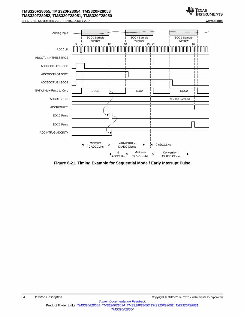
0 2 12
Analog Input
ADCCLK
ADCCTL1.INTPULSEPOS
ADCSOCFLG1.SOC0
ADCSOCFLG1.SOC1
ADCSOCFLG1.SOC2
S/H Window Pulse to Core
ADCRESULT0
ADCRESULT1
EOC0 Pulse
ADCINTFLG.ADCINTx
EOC0 Pulse
SOC0 SampleWindow
SOC1 SampleWindow
SOC2 SampleWindow
SOC0 SOC1 SOC2
Result 0 Latched
Minimum
10 ADCCLKs
Conversion 0
13 ADC Clocks
6
ADCCLKs
Minimum
10 ADCCLKs
Conversion 1
13 ADC Clocks
18 27 28 43
2 ADCCLKs
TMS320F28055, TMS320F28054, TMS320F28053TMS320F28052, TMS320F28051, TMS320F28050SPRS797B –NOVEMBER 2012–REVISED JULY 2014 www.ti.com
Figure 6-21. Timing Example for Sequential Mode / Early Interrupt Pulse
84 Detailed Description Copyright © 2012–2014, Texas Instruments IncorporatedSubmit Documentation Feedback
Product Folder Links: TMS320F28055 TMS320F28054 TMS320F28053 TMS320F28052 TMS320F28051TMS320F28050

0 2 12
Analog Input A
ADCCLK
ADCCTL1.INTPULSEPOS
ADCSOCFLG1.SOC0
ADCSOCFLG1.SOC1
ADCSOCFLG1.SOC2
S/H Window Pulse to Core
ADCRESULT0
ADCRESULT1
EOC0 Pulse
ADCINTFLG.ADCINTx
EOC1 Pulse
SOC0 SampleA Window
SOC0 (A/B)
Result 0 (B) Latched
2 ADCCLKs
25 27 4331 40 56
SOC0 SampleB Window
Analog Input B
ADCRESULT2
EOC2 Pulse
SOC2 (A/B)
Result 0 (A) Latched
1 ADCCLK
SOC2 SampleB Window
SOC2 SampleA Window
Minimum
10 ADCCLKs
Conversion 0 (A)
13 ADC Clocks
19
ADCCLKs
Minimum
10 ADCCLKs
Conversion 1 (A)
13 ADC Clocks
2 ADCCLKsConversion 0 (B)
13 ADC Clocks
TMS320F28055, TMS320F28054, TMS320F28053TMS320F28052, TMS320F28051, TMS320F28050
www.ti.com SPRS797B –NOVEMBER 2012–REVISED JULY 2014
Figure 6-22. Timing Example for Simultaneous Mode / Late Interrupt Pulse
Copyright © 2012–2014, Texas Instruments Incorporated Detailed Description 85Submit Documentation Feedback
Product Folder Links: TMS320F28055 TMS320F28054 TMS320F28053 TMS320F28052 TMS320F28051TMS320F28050

0 2 12
Analog Input A
ADCCLK
ADCCTL1.INTPULSEPOS
ADCSOCFLG1.SOC0
ADCSOCFLG1.SOC1
ADCSOCFLG1.SOC2
S/H Window Pulse to Core
ADCRESULT0
ADCRESULT1
EOC0 Pulse
ADCINTFLG.ADCINTx
EOC1 Pulse
SOC0 SampleA Window
SOC0 (A/B)
Result 0 (B) Latched
2 ADCCLKs
25 27 40 56
SOC0 SampleB Window
Analog Input B
ADCRESULT2
EOC2 Pulse
SOC2 (A/B)
Result 0 (A) Latched
SOC2 SampleB Window
SOC2 SampleA Window
Minimum
10 ADCCLKs
Conversion 0 (A)
13 ADC Clocks
19
ADCCLKs
Minimum
10 ADCCLKs
Conversion 1 (A)
13 ADC Clocks
2 ADCCLKsConversion 0 (B)
13 ADC Clocks
TMS320F28055, TMS320F28054, TMS320F28053TMS320F28052, TMS320F28051, TMS320F28050SPRS797B –NOVEMBER 2012–REVISED JULY 2014 www.ti.com
Figure 6-23. Timing Example for Simultaneous Mode / Early Interrupt Pulse
86 Detailed Description Copyright © 2012–2014, Texas Instruments IncorporatedSubmit Documentation Feedback
Product Folder Links: TMS320F28055 TMS320F28054 TMS320F28053 TMS320F28052 TMS320F28051TMS320F28050

TMS320F28055, TMS320F28054, TMS320F28053TMS320F28052, TMS320F28051, TMS320F28050
www.ti.com SPRS797B –NOVEMBER 2012–REVISED JULY 2014
6.9.2.2 Analog Front End
6.9.2.2.1 AFE Device-Specific Information
The AFE contains up to seven comparators with up to three integrated DACs, one VREFOUT-bufferedDAC, up to four PGAs, and up to four digital filters. Figure 6-24 and Figure 6-25 show the AFE.
The comparator output signal filtering is achieved using the Digital Filter present on selective input lineand qualifies the output of the COMP/DAC subsystem (see Figure 6-27). The filtered or unfiltered outputof the COMP/DAC subsystem can be configured to be an input to the Digital Compare submodule of theePWM peripheral. Note: The Analog inputs are brought in through the AFE subsystem rather than throughan AIO Mux, which is not present.
The ADCINSWITCH register is used to control ADC inputs dynamically and the setting of this register isseparate from the AFE and Digital Filter initialization.
Copyright © 2012–2014, Texas Instruments Incorporated Detailed Description 87Submit Documentation Feedback
Product Folder Links: TMS320F28055 TMS320F28054 TMS320F28053 TMS320F28052 TMS320F28051TMS320F28050

VREFHI
V /A0REFOUT
B7PGA
G~ = 3, 6, 11
_
+Cmp1
_
+Cmp1V
BufferedDAC Output
REFOUTCOMPB7
DFSS
DAC5 6-bit
DAC6 6-bit
B7
VREFHI
A0
PFCGND
B0A2A4B2
A1PGA
G~ = 3, 6, 11
M1GND
A3PGA
G~ = 3, 6, 11
M1GND
B1PGA
G~ = 3, 6, 11
M1GND
A5
ADCCTL1.REFLOCONV
B5
A7
B3
B5
VREFLO
B0A2A4B2
ADC
_
+Cmp2
DAC1 6-bit
COMPA1H
DFSS
_
+Cmp3COMPA1L
DFSSADCIN-SWITCH
A1
Cmp4COMPA3H
DFSS
_
+Cmp5COMPA3L
DFSSA3
_
+Cmp6
COMPB1H
DFSS
_
+Cmp7COMPB1L
DFSSB1
DAC2 6-bit
Temp Sensor
ADCCTL1.TEMPCONV
A5
_
+
ADCIN-SWITCH
ADCIN-SWITCH
A6
B4
B6
ADCIN-SWITCH
VREFLO
A7
B3
A6GAIN AMP
G~ = 3
M2GND
B4GAIN AMP
G~ = 3
M2GND
B6GAIN AMP
G~ = 3
M2GNDLegend
Cmp - Comparator
DFSS - Comparator Trip/Digital Filter Subsystem Block
GAIN AMP - Fixed Gain Amplifier
PGA - Programmable Gain Amplifier
VSSA
RPD
TMS320F28055, TMS320F28054, TMS320F28053TMS320F28052, TMS320F28051, TMS320F28050SPRS797B –NOVEMBER 2012–REVISED JULY 2014 www.ti.com
Figure 6-24. 28055, 28054, 28053, 28052, and 28051 Analog Front End
88 Detailed Description Copyright © 2012–2014, Texas Instruments IncorporatedSubmit Documentation Feedback
Product Folder Links: TMS320F28055 TMS320F28054 TMS320F28053 TMS320F28052 TMS320F28051TMS320F28050

ADC
VREFHI
V /A0REFOUT
_
+Cmp1V
BufferedDAC Output
REFOUT
DAC6 6-bit
VREFHI
A0
B0A2A4B2
A1PGA
G~ = 3, 6, 11
M1GND
_
+Cmp2
DAC1 6-bit
COMPA1H
DFSS
_
+Cmp3COMPA1L
DFSSADCIN-SWITCH
A1
A3PGA
G~ = 3, 6, 11
M1GND
Cmp4COMPA3H
DFSS
_
+Cmp5COMPA3L
DFSSA3
B1PGA
G~ = 3, 6, 11
M1GND
_
+Cmp6
COMPB1H
DFSS
_
+Cmp7COMPB1L
DFSSB1
DAC2 6-bit
Temp Sensor
ADCCTL1.TEMPCONVA5
A5
ADCCTL1.REFLOCONV
B5
A7
B3
B5
VREFLO
B0A2A4B2
_
+
ADCIN-SWITCH
VREFLO
A7
B3
A6GAIN AMP
G~ = 3
M2GND
B4GAIN AMP
G~ = 3
M2GND
B6GAIN AMP
G~ = 3
M2GND
B7GAIN AMP
G~ = 3
PFCGND
B7
Legend
Cmp - Comparator
DFSS - Comparator Trip/Digital Filter Subsystem Block
GAIN AMP - Fixed Gain Amplifier
PGA - Programmable Gain Amplifier
ADCIN-SWITCH
A6
B4
B6
ADCIN-SWITCH
VSSA
RPD
TMS320F28055, TMS320F28054, TMS320F28053TMS320F28052, TMS320F28051, TMS320F28050
www.ti.com SPRS797B –NOVEMBER 2012–REVISED JULY 2014
Figure 6-25. 28050 Analog Front End
Copyright © 2012–2014, Texas Instruments Incorporated Detailed Description 89Submit Documentation Feedback
Product Folder Links: TMS320F28055 TMS320F28054 TMS320F28053 TMS320F28052 TMS320F28051TMS320F28050

ePWM 1-7
DCAH
DCAL
DCBH
DCBL
DCTRIPSEL
GPIOMUX
CTRIPOUTPOL
SYSCLK
Digital Filter
CTRIPOUTBYP 01 CTRIPxxOUTEN
CTRIPOUTxxSTS
CTRIPOUTxxFLG
CTRIPOUTLATEN
0
1
CTRIPFILCTRLREGISTER
CTRIPBYP
0
1
COMPxxPOL
COMPxxH
0
1
COMPxxPOL
COMPxxL
COMPxINPEN
ENABLES
CTRIPEN
(to all ePWM modules)
CTRIPxx0CTLREGISTER
0
1
VREFHI
VSSA
6-bitDAC
+
_
Op Amp
VSSA
RPD
TMS320F28055, TMS320F28054, TMS320F28053TMS320F28052, TMS320F28051, TMS320F28050SPRS797B –NOVEMBER 2012–REVISED JULY 2014 www.ti.com
Figure 6-26. VREFOUT
Figure 6-27. Comparator Trip/Digital Filter Subsystem
90 Detailed Description Copyright © 2012–2014, Texas Instruments IncorporatedSubmit Documentation Feedback
Product Folder Links: TMS320F28055 TMS320F28054 TMS320F28053 TMS320F28052 TMS320F28051TMS320F28050

TMS320F28055, TMS320F28054, TMS320F28053TMS320F28052, TMS320F28051, TMS320F28050
www.ti.com SPRS797B –NOVEMBER 2012–REVISED JULY 2014
6.9.2.2.2 AFE Register Descriptions
Table 6-38. DAC Control Registers
SIZE EALLOWREGISTER NAME ADDRESS DESCRIPTION(x16) PROTECTEDDAC1CTL 0x6400 1 Yes DAC1 Control RegisterDAC2CTL 0x6401 1 Yes DAC2 Control RegisterDAC5CTL 0x6404 1 Yes DAC5 Control RegisterVREFOUTCTL 0x6405 1 Yes VREFOUT DAC Control Register
Table 6-39. DAC, PGA, Comparator, and Filter Enable Registers
SIZE EALLOWREGISTER NAME ADDRESS DESCRIPTION(x16) PROTECTEDDACEN 0x6410 1 Yes DAC Enables RegisterVREFOUTEN 0x6411 1 Yes VREFOUT Enable RegisterPGAEN 0x6412 1 Yes Programmable Gain Amplifier Enable RegisterCOMPEN 0x6413 1 Yes Comparator Enable RegisterAMPM1_GAIN 0x6414 1 Yes Motor Unit 1 PGA Gain Controls RegisterAMP_PFC_GAIN 0x6416 1 Yes PFC PGA Gain Controls Register
Table 6-40. SWITCH Registers
SIZE EALLOWREGISTER NAME ADDRESS DESCRIPTION(x16) PROTECTEDADCINSWITCH 0x6421 1 Yes ADC Input-Select Switch Control Register
0x6422 –Reserved 7 Yes Reserved0x6428COMPHYSTCTL 0x6429 1 Yes Comparator Hysteresis Control Register
Table 6-41. Digital Filter and Comparator Control Registers
SIZE EALLOWREGISTER NAME ADDRESS DESCRIPTION(x16) PROTECTEDCTRIPA1ICTL 0x6430 1 Yes CTRIPA1 Filter Input and Function Control RegisterCTRIPA1FILCTL 0x6431 1 Yes CTRIPA1 Filter Parameters RegisterCTRIPA1FILCLKCTL 0x6432 1 Yes CTRIPA1 Filter Sample Clock Control RegisterReserved 0x6433 1 Yes ReservedCTRIPA3ICTL 0x6434 1 Yes CTRIPA3 Filter Input and Function Control RegisterCTRIPA3FILCTL 0x6435 1 Yes CTRIPA3 Filter Parameters RegisterCTRIPA3FILCLKCTL 0x6436 1 Yes CTRIPA3 Filter Sample Clock Control RegisterReserved 0x6437 1 Yes ReservedCTRIPB1ICTL 0x6438 1 Yes CTRIPB1 Filter Input and Function Control RegisterCTRIPB1FILCTL 0x6439 1 Yes CTRIPB1 Filter Parameters RegisterCTRIPB1FILCLKCTL 0x643A 1 Yes CTRIPB1 Filter Sample Clock Control RegisterReserved 0x643B 1 Yes ReservedReserved 0x643C 1 Yes ReservedCTRIPM1OCTL 0x643D 1 Yes CTRIPM1 CTRIP Filter Output Control RegisterCTRIPM1STS 0x643E 1 Yes CTRIPM1 CTRIPxx Outputs Status RegisterCTRIPM1FLGCLR 0x643F 1 Yes CTRIPM1 CTRIPxx Flag Clear Register
0x6440 –Reserved 16 Yes Reserved0x645F0x6460 –Reserved 16 Yes Reserved0x646F
Copyright © 2012–2014, Texas Instruments Incorporated Detailed Description 91Submit Documentation Feedback
Product Folder Links: TMS320F28055 TMS320F28054 TMS320F28053 TMS320F28052 TMS320F28051TMS320F28050

TMS320F28055, TMS320F28054, TMS320F28053TMS320F28052, TMS320F28051, TMS320F28050SPRS797B –NOVEMBER 2012–REVISED JULY 2014 www.ti.com
Table 6-41. Digital Filter and Comparator Control Registers (continued)SIZE EALLOWREGISTER NAME ADDRESS DESCRIPTION(x16) PROTECTED
CTRIPB7ICTL 0x6470 1 Yes CTRIPB7 Filter Input and Function Control RegisterCTRIPB7FILCTL 0x6471 1 Yes CTRIPB7 Filter Parameters RegisterCTRIPB7FILCLKCTL 0x6472 1 Yes CTRIPB7 Filter Sample Clock Control Register
0x6473 –Reserved 9 Yes Reserved0x647BReserved 0x647C 1 Yes ReservedCTRIPPFCOCTL 0x647D 1 Yes CTRIPPFC CTRIPxx Outputs Status RegisterCTRIPPFCSTS 0x647E 1 Yes CTRIPPFC CTRIPxx Flag Clear RegisterCTRIPPFCFLGCLR 0x647F 1 Yes CTRIPPFC COMP Test Control Register
Table 6-42. LOCK Registers
SIZE EALLOWREGISTER NAME ADDRESS DESCRIPTION(x16) PROTECTEDLOCKCTRIP 0x64F0 1 Yes Lock Register for CTRIP Filters RegisterReserved 0x64F1 1 Yes ReservedLOCKDAC 0x64F2 1 Yes Lock Register for DACs RegisterReserved 0x64F3 1 Yes ReservedLOCKAMPCOMP 0x64F4 1 Yes Lock Register for Amplifiers and Comparators RegisterReserved 0x64F5 1 Yes ReservedLOCKSWITCH 0x64F6 1 Yes Lock Register for Switches Register
92 Detailed Description Copyright © 2012–2014, Texas Instruments IncorporatedSubmit Documentation Feedback
Product Folder Links: TMS320F28055 TMS320F28054 TMS320F28053 TMS320F28052 TMS320F28051TMS320F28050

TMS320F28055, TMS320F28054, TMS320F28053TMS320F28052, TMS320F28051, TMS320F28050
www.ti.com SPRS797B –NOVEMBER 2012–REVISED JULY 2014
6.9.2.2.3 PGA Electrical Data/Timing
Table 6-43. Op-Amp Linear Output and ADC Sampling Time Across Gain Settings
MINIMUMEQUIVALENT GAIN FROM LINEAR OUTPUT RANGE ADC SAMPLING TIMEINTERNAL RESISTOR RATIO INPUT TO OUTPUT OF OP-AMP TO ACHIEVE SETTLING
ACCURACY10 11 0.6 V to VDDA – 0.6 V 384 ns (ACQPS = 23)5 6 0.6 V to VDDA – 0.6 V 384 ns (ACQPS = 23)2 3 0.6 V to VDDA – 0.6 V 384 ns (ACQPS = 23)
Table 6-44. PGA Gain Stage: DC Accuracy Across Gain Settings
COMPENSATED COMPENSATED INPUTEQUIVALENT GAIN FROM GAIN-ERROR ACROSS OFFSET-ERROR ACROSSINTERNAL RESISTOR RATIO INPUT TO OUTPUT TEMPERATURE AND SUPPLY TEMPERATURE AND SUPPLY
VARIATIONS VARIATIONS IN mV10 11 < ±2.5% < ±8 mV5 6 < ±1.5% < ±8 mV2 3 < ±1.0% < ±8 mV
6.9.2.2.4 Comparator Block Electrical Data/Timing
Table 6-45. Electrical Characteristics of the Comparator/DAC
PARAMETER MIN TYP MAX UNITSComparator
Comparator Input Range VSSA – VDDA VComparator response time to PWM Trip Zone (Async) 65 nsComparator large step response time to PWM Trip Zone (Async) 95 ns
DACDAC Output Range VDDA / 26 – VDDA VDAC resolution 6 bitsDAC Gain –1.5 %DAC Offset 10 mVMonotonic YesINL 0.2 LSB
Copyright © 2012–2014, Texas Instruments Incorporated Detailed Description 93Submit Documentation Feedback
Product Folder Links: TMS320F28055 TMS320F28054 TMS320F28053 TMS320F28052 TMS320F28051TMS320F28050

TMS320F28055, TMS320F28054, TMS320F28053TMS320F28052, TMS320F28051, TMS320F28050SPRS797B –NOVEMBER 2012–REVISED JULY 2014 www.ti.com
6.9.2.2.5 VREFOUT Buffered DAC Electrical Data
Table 6-46. Electrical Characteristics of VREFOUT Buffered DAC
PARAMETER MIN TYP MAX UNITSVREFOUT Programmable Range 6 56 LSBVREFOUT resolution 6 bitsVREFOUT Gain –1.5 %VREFOUT Offset 10 mVMonotonic YesINL ±0.2 LSB
3 kΩLoad
100 pFRPD 20 kΩ
94 Detailed Description Copyright © 2012–2014, Texas Instruments IncorporatedSubmit Documentation Feedback
Product Folder Links: TMS320F28055 TMS320F28054 TMS320F28053 TMS320F28052 TMS320F28051TMS320F28050
6.02
1.76)(SINADN
-
=
TMS320F28055, TMS320F28054, TMS320F28053TMS320F28052, TMS320F28051, TMS320F28050
www.ti.com SPRS797B –NOVEMBER 2012–REVISED JULY 2014
6.9.3 Detailed DescriptionsIntegral Nonlinearity
Integral nonlinearity refers to the deviation of each individual code from a line drawn from zero through fullscale. The point used as zero occurs one-half LSB before the first code transition. The full-scale point isdefined as level one-half LSB beyond the last code transition. The deviation is measured from the centerof each particular code to the true straight line between these two points.
Differential Nonlinearity
An ideal ADC exhibits code transitions that are exactly 1 LSB apart. DNL is the deviation from this idealvalue. A differential nonlinearity error of less than ±1 LSB ensures no missing codes.
Zero Offset
Zero error is the difference between the ideal input voltage and the actual input voltage that just causes atransition from an output code of zero to an output code of one.
Gain Error
The first code transition should occur at an analog value one-half LSB above negative full scale. The lasttransition should occur at an analog value one and one-half LSB below the nominal full scale. Gain error isthe deviation of the actual difference between first and last code transitions and the ideal differencebetween first and last code transitions.
Signal-to-Noise Ratio + Distortion
Signal-to-noise ratio + distortion (SINAD) is the ratio of the rms value of the measured input signal to therms sum of all other spectral components below the Nyquist frequency, including harmonics but excludingdc. The value for SINAD is expressed in decibels.
Effective Number of Bits
For a sine wave, SINAD can be expressed in terms of the number of bits. Using the following formula,
it is possible to get a measure of performance expressed as N, the effective number ofbits (ENOB). Thus, the ENOB for a device for sine wave inputs at a given input frequency can becalculated directly from its measured SINAD.
Total Harmonic Distortion
Total harmonic distortion (THD) is the ratio of the rms sum of the first nine harmonic components to therms value of the measured input signal and is expressed as a percentage or in decibels.
Spurious Free Dynamic Range
Spurious free dynamic range (SFDR) is the difference in dB between the rms amplitude of the input signaland the peak spurious signal.
Copyright © 2012–2014, Texas Instruments Incorporated Detailed Description 95Submit Documentation Feedback
Product Folder Links: TMS320F28055 TMS320F28054 TMS320F28053 TMS320F28052 TMS320F28051TMS320F28050

1)(SPIBRR
LSPCLKrateBaud
+
= 127to3SPIBRRwhen =
4
LSPCLKrateBaud = 21,0,SPIBRRwhen =
TMS320F28055, TMS320F28054, TMS320F28053TMS320F28052, TMS320F28051, TMS320F28050SPRS797B –NOVEMBER 2012–REVISED JULY 2014 www.ti.com
6.9.4 Serial Peripheral Interface
6.9.4.1 SPI Device-Specific Information
The device includes the four-pin SPI module. The SPI is a high-speed, synchronous serial I/O port thatallows a serial bit stream of programmed length (one to sixteen bits) to be shifted into and out of thedevice at a programmable bit-transfer rate. Normally, the SPI is used for communications between theMCU and external peripherals or another processor. Typical applications include external I/O or peripheralexpansion through devices such as shift registers, display drivers, and ADCs. Multidevice communicationsare supported by the master/slave operation of the SPI.
The SPI module features include:• Four external pins:
– SPISOMI: SPI slave-output/master-input pin– SPISIMO: SPI slave-input/master-output pin– SPISTE: SPI slave transmit-enable pin– SPICLK: SPI serial-clock pin
NOTE: All four pins can be used as GPIO if the SPI module is not used.• Two operational modes: master and slave
Baud rate: 125 different programmable rates.
• Data word length: one to sixteen data bits• Four clocking schemes (controlled by clock polarity and clock phase bits) include:
– Falling edge without phase delay: SPICLK active-high. SPI transmits data on the falling edge of theSPICLK signal and receives data on the rising edge of the SPICLK signal.
– Falling edge with phase delay: SPICLK active-high. SPI transmits data one half-cycle ahead of thefalling edge of the SPICLK signal and receives data on the falling edge of the SPICLK signal.
– Rising edge without phase delay: SPICLK inactive-low. SPI transmits data on the rising edge of theSPICLK signal and receives data on the falling edge of the SPICLK signal.
– Rising edge with phase delay: SPICLK inactive-low. SPI transmits data one half-cycle ahead of thefalling edge of the SPICLK signal and receives data on the rising edge of the SPICLK signal.
• Simultaneous receive and transmit operation (transmit function can be disabled in software)• Transmitter and receiver operations are accomplished through either interrupt-driven or polled
algorithms.• Nine SPI module control registers: Located in control register frame beginning at address 7040h.
NOTEAll registers in this module are 16-bit registers that are connected to Peripheral Frame 2.When a register is accessed, the register data is in the lower byte (7–0), and the upper byte(15–8) is read as zeros. Writing to the upper byte has no effect.
Enhanced feature:• 4-level transmit/receive FIFO• Delayed transmit control• Bi-directional 3-wire SPI mode support• Audio data receive support via SPISTE inversion
96 Detailed Description Copyright © 2012–2014, Texas Instruments IncorporatedSubmit Documentation Feedback
Product Folder Links: TMS320F28055 TMS320F28054 TMS320F28053 TMS320F28052 TMS320F28051TMS320F28050

S
SPICTL.0
SPI INT FLAG
SPI INTENA
SPISTS.6
S
ClockPolarity
Talk
LSPCLK
SPI Bit Rate
State Control
ClockPhase
ReceiverOverrun Flag
SPICTL.4
OverrunINT ENA
SPICCR.3 - 0
SPIBRR.6 - 0 SPICCR.6 SPICTL.3
SPIDAT.15 - 0
SPICTL.1
M
S
M
Master/Slave
SPISTS.7
SPIDATData Register
M
S
SPICTL.2SPI Char
SPISIMO
SPISOMI
SPICLK
SW2
S
M
M
S
SW3
To CPU
M
SW1
RX FIFO _0
RX FIFO _1
-----
RX FIFO _3
TX FIFO Registers
TX FIFO _0
TX FIFO _1-----
TX FIFO _3
RX FIFO Registers
16
16
16
TX InterruptLogic
RX InterruptLogic
SPIINT
SPITX
SPIFFOVFFLAG
SPIFFRX.15
TX FIFO Interrupt
RX FIFO Interrupt
SPIRXBUF
SPITXBUF
SPIFFTX.14
SPIFFENA
SPISTE
16
0123
0123456
TW
TWTW
SPIPRI.0
TRIWIRE
SPIPRI.1
STEINV
STEINV
SPIRXBUFBuffer Register
SPITXBUFBuffer Register
TMS320F28055, TMS320F28054, TMS320F28053TMS320F28052, TMS320F28051, TMS320F28050
www.ti.com SPRS797B –NOVEMBER 2012–REVISED JULY 2014
Figure 6-28 is a block diagram of the SPI in slave mode.
A. SPISTE is driven low by the master for a slave device.
Figure 6-28. SPI Module Block Diagram (Slave Mode)
Copyright © 2012–2014, Texas Instruments Incorporated Detailed Description 97Submit Documentation Feedback
Product Folder Links: TMS320F28055 TMS320F28054 TMS320F28053 TMS320F28052 TMS320F28051TMS320F28050

TMS320F28055, TMS320F28054, TMS320F28053TMS320F28052, TMS320F28051, TMS320F28050SPRS797B –NOVEMBER 2012–REVISED JULY 2014 www.ti.com
6.9.4.2 SPI Register Descriptions
The SPI port operation is configured and controlled by the registers listed in Table 6-47.
Table 6-47. SPI-A Registers
NAME ADDRESS SIZE (x16) EALLOW PROTECTED DESCRIPTION (1)
SPICCR 0x7040 1 No SPI-A Configuration Control RegisterSPICTL 0x7041 1 No SPI-A Operation Control RegisterSPISTS 0x7042 1 No SPI-A Status RegisterSPIBRR 0x7044 1 No SPI-A Baud Rate Register
SPIRXEMU 0x7046 1 No SPI-A Receive Emulation Buffer RegisterSPIRXBUF 0x7047 1 No SPI-A Serial Input Buffer RegisterSPITXBUF 0x7048 1 No SPI-A Serial Output Buffer Register
SPIDAT 0x7049 1 No SPI-A Serial Data RegisterSPIFFTX 0x704A 1 No SPI-A FIFO Transmit RegisterSPIFFRX 0x704B 1 No SPI-A FIFO Receive RegisterSPIFFCT 0x704C 1 No SPI-A FIFO Control RegisterSPIPRI 0x704F 1 No SPI-A Priority Control Register
(1) Registers in this table are mapped to Peripheral Frame 2. This space only allows 16-bit accesses. 32-bit accesses produce undefinedresults.
6.9.4.3 SPI Master Mode Electrical Data/Timing
Table 6-48 lists the master mode timing (clock phase = 0) and Table 6-49 lists the timing (clockphase = 1). Figure 6-29 and Figure 6-30 show the timing waveforms.
98 Detailed Description Copyright © 2012–2014, Texas Instruments IncorporatedSubmit Documentation Feedback
Product Folder Links: TMS320F28055 TMS320F28054 TMS320F28053 TMS320F28052 TMS320F28051TMS320F28050

TMS320F28055, TMS320F28054, TMS320F28053TMS320F28052, TMS320F28051, TMS320F28050
www.ti.com SPRS797B –NOVEMBER 2012–REVISED JULY 2014
Table 6-48. SPI Master Mode External Timing (Clock Phase = 0) (1) (2) (3) (4) (5)
SPI WHEN (SPIBRR + 1) IS EVEN OR SPI WHEN (SPIBRR + 1) IS ODDSPIBRR = 0 OR 2 AND SPIBRR > 3NO. UNIT
MIN MAX MIN MAX1 tc(SPC)M Cycle time, SPICLK 4tc(LCO) 128tc(LCO) 5tc(LCO) 127tc(LCO) ns2 tw(SPCH)M Pulse duration, SPICLK high 0.5tc(SPC)M – 10 0.5tc(SPC)M 0.5tc(SPC)M – 0.5tc(LCO) – 10 0.5tc(SPC)M – 0.5tc(LCO) ns
(clock polarity = 0)tw(SPCL)M Pulse duration, SPICLK low 0.5tc(SPC)M – 10 0.5tc(SPC)M 0.5tc(SPC)M – 0.5tc(LCO) – 10 0.5tc(SPC)M – 0.5tc(LCO)
(clock polarity = 1)3 tw(SPCL)M Pulse duration, SPICLK low 0.5tc(SPC)M – 10 0.5tc(SPC)M 0.5tc(SPC)M + 0.5tc(LCO) – 10 0.5tc(SPC)M + 0.5tc(LCO) ns
(clock polarity = 0)tw(SPCH)M Pulse duration, SPICLK high 0.5tc(SPC)M – 10 0.5tc(SPC)M 0.5tc(SPC)M + 0.5tc(LCO) – 10 0.5tc(SPC)M + 0.5tc(LCO)
(clock polarity = 1)4 td(SPCH-SIMO)M Delay time, SPICLK high to SPISIMO 10 10 ns
valid (clock polarity = 0)td(SPCL-SIMO)M Delay time, SPICLK low to SPISIMO 10 10
valid (clock polarity = 1)5 tv(SPCL-SIMO)M Valid time, SPISIMO data valid after 0.5tc(SPC)M – 10 0.5tc(SPC)M + 0.5tc(LCO) – 10 ns
SPICLK low (clock polarity = 0)tv(SPCH-SIMO)M Valid time, SPISIMO data valid after 0.5tc(SPC)M – 10 0.5tc(SPC)M + 0.5tc(LCO) – 10
SPICLK high (clock polarity = 1)8 tsu(SOMI-SPCL)M Setup time, SPISOMI before SPICLK 26 26 ns
low (clock polarity = 0)tsu(SOMI-SPCH)M Setup time, SPISOMI before SPICLK 26 26
high (clock polarity = 1)9 tv(SPCL-SOMI)M Valid time, SPISOMI data valid after 0.25tc(SPC)M – 10 0.5tc(SPC)M – 0.5tc(LCO) – 10 ns
SPICLK low (clock polarity = 0)tv(SPCH-SOMI)M Valid time, SPISOMI data valid after 0.25tc(SPC)M – 10 0.5tc(SPC)M – 0.5tc(LCO) – 10
SPICLK high (clock polarity = 1)
(1) The MASTER / SLAVE bit (SPICTL.2) is set and the CLOCK PHASE bit (SPICTL.3) is cleared.(2) tc(SPC) = SPI clock cycle time = LSPCLK/4 or LSPCLK/(SPIBRR +1)(3) tc(LCO) = LSPCLK cycle time(4) Internal clock prescalers must be adjusted such that the SPI clock speed is limited to the following SPI clock rate:
Master mode transmit 15-MHz MAX, master mode receive 10-MHz MAXSlave mode transmit 10-MHz MAX, slave mode receive 10-MHz MAX.
(5) The active edge of the SPICLK signal referenced is controlled by the clock polarity bit (SPICCR.6).
Copyright © 2012–2014, Texas Instruments Incorporated Detailed Description 99Submit Documentation Feedback
Product Folder Links: TMS320F28055 TMS320F28054 TMS320F28053 TMS320F28052 TMS320F28051TMS320F28050

9
4
SPISOMI
SPISIMO
SPICLK(clock polarity = 1)
SPICLK(clock polarity = 0)
Master In DataMust Be Valid
Master Out Data Is Valid
SPISTE(A)
1
2
3
5
8
TMS320F28055, TMS320F28054, TMS320F28053TMS320F28052, TMS320F28051, TMS320F28050SPRS797B –NOVEMBER 2012–REVISED JULY 2014 www.ti.com
A. In the master mode, SPISTE goes active 0.5tc(SPC) (minimum) before valid SPI clock edge. On the trailing end of the word, the SPISTE will go inactive 0.5tc(SPC) afterthe receiving edge (SPICLK) of the last data bit, except that SPISTE stays active between back-to-back transmit words in both FIFO and non-FIFO modes.
Figure 6-29. SPI Master Mode External Timing (Clock Phase = 0)
100 Detailed Description Copyright © 2012–2014, Texas Instruments IncorporatedSubmit Documentation Feedback
Product Folder Links: TMS320F28055 TMS320F28054 TMS320F28053 TMS320F28052 TMS320F28051TMS320F28050

TMS320F28055, TMS320F28054, TMS320F28053TMS320F28052, TMS320F28051, TMS320F28050
www.ti.com SPRS797B –NOVEMBER 2012–REVISED JULY 2014
Table 6-49. SPI Master Mode External Timing (Clock Phase = 1) (1) (2) (3) (4) (5)
SPI WHEN (SPIBRR + 1) IS EVEN SPI WHEN (SPIBRR + 1) IS ODDOR SPIBRR = 0 OR 2 AND SPIBRR > 3NO. UNIT
MIN MAX MIN MAX1 tc(SPC)M Cycle time, SPICLK 4tc(LCO) 128tc(LCO) 5tc(LCO) 127tc(LCO) ns2 tw(SPCH)M Pulse duration, SPICLK high 0.5tc(SPC)M – 10 0.5tc(SPC)M 0.5tc(SPC)M – 0.5tc (LCO) – 10 0.5tc(SPC)M – 0.5tc(LCO) ns
(clock polarity = 0)tw(SPCL))M Pulse duration, SPICLK low 0.5tc(SPC)M – 10 0.5tc(SPC)M 0.5tc(SPC)M – 0.5tc (LCO) – 10 0.5tc(SPC)M – 0.5tc(LCO
(clock polarity = 1)3 tw(SPCL)M Pulse duration, SPICLK low 0.5tc(SPC)M – 10 0.5tc(SPC)M 0.5tc(SPC)M + 0.5tc(LCO) – 10 0.5tc(SPC)M + 0.5tc(LCO) ns
(clock polarity = 0)tw(SPCH)M Pulse duration, SPICLK high 0.5tc(SPC)M – 10 0.5tc(SPC)M 0.5tc(SPC)M + 0.5tc(LCO) – 10 0.5tc(SPC)M + 0.5tc(LCO)
(clock polarity = 1)6 tsu(SIMO-SPCH)M Setup time, SPISIMO data valid 0.5tc(SPC)M – 10 0.5tc(SPC)M – 10 ns
before SPICLK high(clock polarity = 0)
tsu(SIMO-SPCL)M Setup time, SPISIMO data valid 0.5tc(SPC)M – 10 0.5tc(SPC)M – 10before SPICLK low(clock polarity = 1)
7 tv(SPCH-SIMO)M Valid time, SPISIMO data valid after 0.5tc(SPC)M – 10 0.5tc(SPC)M – 10 nsSPICLK high (clock polarity = 0)
tv(SPCL-SIMO)M Valid time, SPISIMO data valid after 0.5tc(SPC)M – 10 0.5tc(SPC)M – 10SPICLK low (clock polarity = 1)
10 tsu(SOMI-SPCH)M Setup time, SPISOMI before 26 26 nsSPICLK high (clock polarity = 0)
tsu(SOMI-SPCL)M Setup time, SPISOMI before 26 26SPICLK low (clock polarity = 1)
11 tv(SPCH-SOMI)M Valid time, SPISOMI data valid after 0.25tc(SPC)M – 10 0.5tc(SPC)M – 10 nsSPICLK high (clock polarity = 0)
tv(SPCL-SOMI)M Valid time, SPISOMI data valid after 0.25tc(SPC)M – 10 0.5tc(SPC)M – 10SPICLK low (clock polarity = 1)
(1) The MASTER/SLAVE bit (SPICTL.2) is set and the CLOCK PHASE bit (SPICTL.3) is set.(2) tc(SPC) = SPI clock cycle time = LSPCLK/4 or LSPCLK/(SPIBRR + 1)(3) Internal clock prescalers must be adjusted such that the SPI clock speed is limited to the following SPI clock rate:
Master mode transmit 15-MHz MAX, master mode receive 10-MHz MAXSlave mode transmit 10-MHz MAX, slave mode receive 10-MHz MAX.
(4) tc(LCO) = LSPCLK cycle time(5) The active edge of the SPICLK signal referenced is controlled by the CLOCK POLARITY bit (SPICCR.6).
Copyright © 2012–2014, Texas Instruments Incorporated Detailed Description 101Submit Documentation Feedback
Product Folder Links: TMS320F28055 TMS320F28054 TMS320F28053 TMS320F28052 TMS320F28051TMS320F28050

Data Valid
11
SPISOMI
SPISIMO
SPICLK
(clock polarity = 1)
SPICLK
(clock polarity = 0)
Master in data
must be valid
Master out data Is valid
1
7
6
10
3
2
SPISTE(A)
TMS320F28055, TMS320F28054, TMS320F28053TMS320F28052, TMS320F28051, TMS320F28050SPRS797B –NOVEMBER 2012–REVISED JULY 2014 www.ti.com
A. In the master mode, SPISTE goes active 0.5tc(SPC) (minimum) before valid SPI clock edge. On the trailing end of the word, the SPISTE will go inactive 0.5tc(SPC) afterthe receiving edge (SPICLK) of the last data bit, except that SPISTE stays active between back-to-back transmit words in both FIFO and non-FIFO modes.
Figure 6-30. SPI Master Mode External Timing (Clock Phase = 1)
102 Detailed Description Copyright © 2012–2014, Texas Instruments IncorporatedSubmit Documentation Feedback
Product Folder Links: TMS320F28055 TMS320F28054 TMS320F28053 TMS320F28052 TMS320F28051TMS320F28050

20
15
SPISIMO
SPISOMI
SPICLK
(clock polarity = 1)
SPICLK
(clock polarity = 0)
SPISIMO datamust be valid
SPISOMI data Is valid
19
16
14
13
12
SPISTE(A)
TMS320F28055, TMS320F28054, TMS320F28053TMS320F28052, TMS320F28051, TMS320F28050
www.ti.com SPRS797B –NOVEMBER 2012–REVISED JULY 2014
6.9.4.4 SPI Slave Mode Electrical Data/Timing
Table 6-50 lists the slave mode external timing (clock phase = 0) and Table 6-51 (clock phase = 1).Figure 6-31 and Figure 6-32 show the timing waveforms.
Table 6-50. SPI Slave Mode External Timing (Clock Phase = 0) (1) (2) (3) (4) (5)
NO. MIN MAX UNIT12 tc(SPC)S Cycle time, SPICLK 4tc(LCO) ns13 tw(SPCH)S Pulse duration, SPICLK high (clock polarity = 0) 0.5tc(SPC)S – 10 0.5tc(SPC)S ns
tw(SPCL)S Pulse duration, SPICLK low (clock polarity = 1) 0.5tc(SPC)S – 10 0.5tc(SPC)S
14 tw(SPCL)S Pulse duration, SPICLK low (clock polarity = 0) 0.5tc(SPC)S – 10 0.5tc(SPC)S nstw(SPCH)S Pulse duration, SPICLK high (clock polarity = 1) 0.5tc(SPC)S – 10 0.5tc(SPC)S
15 td(SPCH-SOMI)S Delay time, SPICLK high to SPISOMI valid (clock polarity = 0) 21 nstd(SPCL-SOMI)S Delay time, SPICLK low to SPISOMI valid (clock polarity = 1) 21
16 tv(SPCL-SOMI)S Valid time, SPISOMI data valid after SPICLK low (clock polarity = 0) 0.75tc(SPC)S nstv(SPCH-SOMI)S Valid time, SPISOMI data valid after SPICLK high (clock polarity = 1) 0.75tc(SPC)S
19 tsu(SIMO-SPCL)S Setup time, SPISIMO before SPICLK low (clock polarity = 0) 26 nstsu(SIMO-SPCH)S Setup time, SPISIMO before SPICLK high (clock polarity = 1) 26
20 tv(SPCL-SIMO)S Valid time, SPISIMO data valid after SPICLK low (clock polarity = 0) 0.5tc(SPC)S – 10 nstv(SPCH-SIMO)S Valid time, SPISIMO data valid after SPICLK high (clock polarity = 1) 0.5tc(SPC)S – 10
(1) The MASTER / SLAVE bit (SPICTL.2) is cleared and the CLOCK PHASE bit (SPICTL.3) is cleared.(2) tc(SPC) = SPI clock cycle time = LSPCLK/4 or LSPCLK/(SPIBRR + 1)(3) Internal clock prescalers must be adjusted such that the SPI clock speed is limited to the following SPI clock rate:
Master mode transmit 15-MHz MAX, master mode receive 10-MHz MAXSlave mode transmit 10-MHz MAX, slave mode receive 10-MHz MAX.
(4) tc(LCO) = LSPCLK cycle time(5) The active edge of the SPICLK signal referenced is controlled by the CLOCK POLARITY bit (SPICCR.6).
A. In the slave mode, the SPISTE signal should be asserted low at least 0.5tc(SPC) (minimum) before the valid SPI clockedge and remain low for at least 0.5tc(SPC) after the receiving edge (SPICLK) of the last data bit.
Figure 6-31. SPI Slave Mode External Timing (Clock Phase = 0)
Copyright © 2012–2014, Texas Instruments Incorporated Detailed Description 103Submit Documentation Feedback
Product Folder Links: TMS320F28055 TMS320F28054 TMS320F28053 TMS320F28052 TMS320F28051TMS320F28050

Data Valid
22
SPISIMO
SPISOMI
SPICLK
(clock polarity = 1)
SPICLK
(clock polarity = 0)
SPISIMO data
must be valid
SPISOMI data is valid
21
12
18
17
14
13
SPISTE(A)
TMS320F28055, TMS320F28054, TMS320F28053TMS320F28052, TMS320F28051, TMS320F28050SPRS797B –NOVEMBER 2012–REVISED JULY 2014 www.ti.com
Table 6-51. SPI Slave Mode External Timing (Clock Phase = 1) (1) (2) (3) (4)
NO. MIN MAX UNIT12 tc(SPC)S Cycle time, SPICLK 8tc(LCO) ns13 tw(SPCH)S Pulse duration, SPICLK high (clock polarity = 0) 0.5tc(SPC)S – 10 0.5tc(SPC)S ns
tw(SPCL)S Pulse duration, SPICLK low (clock polarity = 1) 0.5tc(SPC)S – 10 0.5tc(SPC) S
14 tw(SPCL)S Pulse duration, SPICLK low (clock polarity = 0) 0.5tc(SPC)S – 10 0.5tc(SPC) S nstw(SPCH)S Pulse duration, SPICLK high (clock polarity = 1) 0.5tc(SPC)S – 10 0.5tc(SPC)S
17 tsu(SOMI-SPCH)S Setup time, SPISOMI before SPICLK high (clock polarity = 0) 0.125tc(SPC)S nstsu(SOMI-SPCL)S Setup time, SPISOMI before SPICLK low (clock polarity = 1) 0.125tc(SPC)S
18 tv(SPCL-SOMI)S Valid time, SPISOMI data valid after SPICLK low 0.75tc(SPC)S ns(clock polarity = 1)
tv(SPCH-SOMI)S Valid time, SPISOMI data valid after SPICLK high 0.75tc(SPC) S(clock polarity = 0)
21 tsu(SIMO-SPCH)S Setup time, SPISIMO before SPICLK high (clock polarity = 0) 26 nstsu(SIMO-SPCL)S Setup time, SPISIMO before SPICLK low (clock polarity = 1) 26
22 tv(SPCH-SIMO)S Valid time, SPISIMO data valid after SPICLK high 0.5tc(SPC)S – 10 ns(clock polarity = 0)
tv(SPCL-SIMO)S Valid time, SPISIMO data valid after SPICLK low 0.5tc(SPC)S – 10(clock polarity = 1)
(1) The MASTER / SLAVE bit (SPICTL.2) is cleared and the CLOCK PHASE bit (SPICTL.3) is cleared.(2) tc(SPC) = SPI clock cycle time = LSPCLK/4 or LSPCLK/(SPIBRR + 1)(3) Internal clock prescalers must be adjusted such that the SPI clock speed is limited to the following SPI clock rate:
Master mode transmit 15-MHz MAX, master mode receive 10-MHz MAXSlave mode transmit 10-MHz MAX, slave mode receive 10-MHz MAX.
(4) The active edge of the SPICLK signal referenced is controlled by the CLOCK POLARITY bit (SPICCR.6).
A. In the slave mode, the SPISTE signal should be asserted low at least 0.5tc(SPC) before the valid SPI clock edge andremain low for at least 0.5tc(SPC) after the receiving edge (SPICLK) of the last data bit.
Figure 6-32. SPI Slave Mode External Timing (Clock Phase = 1)
104 Detailed Description Copyright © 2012–2014, Texas Instruments IncorporatedSubmit Documentation Feedback
Product Folder Links: TMS320F28055 TMS320F28054 TMS320F28053 TMS320F28052 TMS320F28051TMS320F28050
8*1)(BRR
LSPCLKrateBaud
+
= 0BRRwhen ¹
16
LSPCLKrateBaud = 0BRRwhen =
TMS320F28055, TMS320F28054, TMS320F28053TMS320F28052, TMS320F28051, TMS320F28050
www.ti.com SPRS797B –NOVEMBER 2012–REVISED JULY 2014
6.9.5 Serial Communications Interface
6.9.5.1 SCI Device-Specific Information
The 2805x devices include three SCI modules (SCI-A, SCI-B, SCI-C). Each SCI module supports digitalcommunications between the CPU and other asynchronous peripherals that use the standard non-return-to-zero (NRZ) format. The SCI receiver and transmitter are double-buffered, and each has its ownseparate enable and interrupt bits. Both can be operated independently or simultaneously in the full-duplex mode. To ensure data integrity, the SCI checks received data for break detection, parity, overrun,and framing errors. The bit rate is programmable to over 65000 different speeds through a 16-bit baud-select register.
Features of each SCI module include:• Two external pins:
– SCITXD: SCI transmit-output pin– SCIRXD: SCI receive-input pin
NOTE: Both pins can be used as GPIO if not used for SCI.– Baud rate programmable to 64K different rates:
• Data-word format– One start bit– Data-word length programmable from one to eight bits– Optional even/odd/no parity bit– One or two stop bits
• Four error-detection flags: parity, overrun, framing, and break detection• Two wake-up multiprocessor modes: idle-line and address bit• Half- or full-duplex operation• Double-buffered receive and transmit functions• Transmitter and receiver operations can be accomplished through interrupt-driven or polled algorithms
with status flags.– Transmitter: TXRDY flag (transmitter-buffer register is ready to receive another character) and TX
EMPTY flag (transmitter-shift register is empty)– Receiver: RXRDY flag (receiver-buffer register is ready to receive another character), BRKDT flag
(break condition occurred), and RX ERROR flag (monitoring four interrupt conditions)• Separate enable bits for transmitter and receiver interrupts (except BRKDT)• NRZ format
NOTEAll registers in this module are 8-bit registers that are connected to Peripheral Frame 2.When a register is accessed, the register data is in the lower byte (7–0), and the upper byte(15–8) is read as zeros. Writing to the upper byte has no effect.
Enhanced features:• Auto baud-detect hardware logic• 4-level transmit/receive FIFO
Copyright © 2012–2014, Texas Instruments Incorporated Detailed Description 105Submit Documentation Feedback
Product Folder Links: TMS320F28055 TMS320F28054 TMS320F28053 TMS320F28052 TMS320F28051TMS320F28050

TX FIFO _0
LSPCLK
WUT
Frame Format and Mode
Even/Odd EnableParity
SCI RX Interrupt select logic
BRKDT
RXRDY
SCIRXST.6
SCICTL1.3
8SCICTL2.1
RX/BK INT ENA
SCIRXD
SCIRXST.1
TXENA
SCI TX Interrupt select logic
TX EMPTY
TXRDY
SCICTL2.0
TX INT ENA
SCITXD
RXENA
SCIRXD
RXWAKE
SCICTL1.6
RX ERR INT ENA
TXWAKE
SCITXD
SCICCR.6 SCICCR.5
SCITXBUF.7-0
SCIHBAUD. 15 - 8
Baud RateMSbyteRegister
SCILBAUD. 7 - 0
Transmitter-DataBuffer Register
8 SCICTL2.6
SCICTL2.7
Baud RateLSbyte
Register
RXSHFRegister
TXSHFRegister
SCIRXST.5
1 TX FIFO _1
-----
TX FIFO _3
8
TX FIFO registers
TX FIFO
TX InterruptLogic
TXINT
SCIFFTX.14
RX FIFO _3
SCIRXBUF.7-0
Receive Data
Buffer registerSCIRXBUF.7-0
-----RX FIFO_1
RX FIFO _0
8
RX FIFO registers
SCICTL1.0
RX Interrupt
Logic
RXINT
RX FIFO
SCIFFRX.15
RXFFOVF
RX Error
SCIRXST.7
PEFE OERX Error
SCIRXST.4 - 2
To CPU
To CPU
AutoBaud Detect logic
SCICTL1.1
SCIFFENA
Interrupts
Interrupts
TMS320F28055, TMS320F28054, TMS320F28053TMS320F28052, TMS320F28051, TMS320F28050SPRS797B –NOVEMBER 2012–REVISED JULY 2014 www.ti.com
Figure 6-33 shows the SCI module block diagram.
Figure 6-33. SCI Module Block Diagram
106 Detailed Description Copyright © 2012–2014, Texas Instruments IncorporatedSubmit Documentation Feedback
Product Folder Links: TMS320F28055 TMS320F28054 TMS320F28053 TMS320F28052 TMS320F28051TMS320F28050

TMS320F28055, TMS320F28054, TMS320F28053TMS320F28052, TMS320F28051, TMS320F28050
www.ti.com SPRS797B –NOVEMBER 2012–REVISED JULY 2014
6.9.5.2 SCI Register Descriptions
The SCI port operation is configured and controlled by the registers listed in Table 6-52.
Table 6-52. SCI-A Registers (1)
EALLOWNAME ADDRESS SIZE (x16) DESCRIPTIONPROTECTEDSCICCRA 0x7050 1 No SCI-A Communications Control RegisterSCICTL1A 0x7051 1 No SCI-A Control Register 1
SCIHBAUDA 0x7052 1 No SCI-A Baud Register, High BitsSCILBAUDA 0x7053 1 No SCI-A Baud Register, Low BitsSCICTL2A 0x7054 1 No SCI-A Control Register 2SCIRXSTA 0x7055 1 No SCI-A Receive Status Register
SCIRXEMUA 0x7056 1 No SCI-A Receive Emulation Data Buffer RegisterSCIRXBUFA 0x7057 1 No SCI-A Receive Data Buffer RegisterSCITXBUFA 0x7059 1 No SCI-A Transmit Data Buffer RegisterSCIFFTXA (2) 0x705A 1 No SCI-A FIFO Transmit RegisterSCIFFRXA (2) 0x705B 1 No SCI-A FIFO Receive RegisterSCIFFCTA (2) 0x705C 1 No SCI-A FIFO Control Register
SCIPRIA 0x705F 1 No SCI-A Priority Control Register
(1) Registers in this table are mapped to Peripheral Frame 2 space. This space only allows 16-bit accesses. 32-bit accesses produceundefined results.
(2) These registers are new registers for the FIFO mode.
Copyright © 2012–2014, Texas Instruments Incorporated Detailed Description 107Submit Documentation Feedback
Product Folder Links: TMS320F28055 TMS320F28054 TMS320F28053 TMS320F28052 TMS320F28051TMS320F28050

TMS320F28055, TMS320F28054, TMS320F28053TMS320F28052, TMS320F28051, TMS320F28050SPRS797B –NOVEMBER 2012–REVISED JULY 2014 www.ti.com
6.9.6 Enhanced Controller Area Network
6.9.6.1 eCAN Device-Specific Information
The CAN module (eCAN-A) has the following features:• Fully compliant with CAN protocol, version 2.0B• Supports data rates up to 1 Mbps• Thirty-two mailboxes, each with the following properties:
– Configurable as receive or transmit– Configurable with standard or extended identifier– Has a programmable receive mask– Supports data and remote frame– Composed of 0 to 8 bytes of data– Uses a 32-bit time stamp on receive and transmit message– Protects against reception of new message– Holds the dynamically programmable priority of transmit message– Employs a programmable interrupt scheme with two interrupt levels– Employs a programmable alarm on transmission or reception time-out
• Low-power mode• Programmable wake-up on bus activity• Automatic reply to a remote request message• Automatic retransmission of a frame in case of loss of arbitration or error• 32-bit local network time counter synchronized by a specific message (communication in conjunction
with mailbox 16)• Self-test mode
– Operates in a loopback mode receiving its own message. A "dummy" acknowledge is provided,thereby eliminating the need for another node to provide the acknowledge bit.
NOTEFor a SYSCLKOUT of 60 MHz, the smallest bit rate possible is 4.6875 kbps.
The F2805x CAN has passed the conformance test per ISO/DIS 16845. Contact TI for test report andexceptions.
108 Detailed Description Copyright © 2012–2014, Texas Instruments IncorporatedSubmit Documentation Feedback
Product Folder Links: TMS320F28055 TMS320F28054 TMS320F28053 TMS320F28052 TMS320F28051TMS320F28050
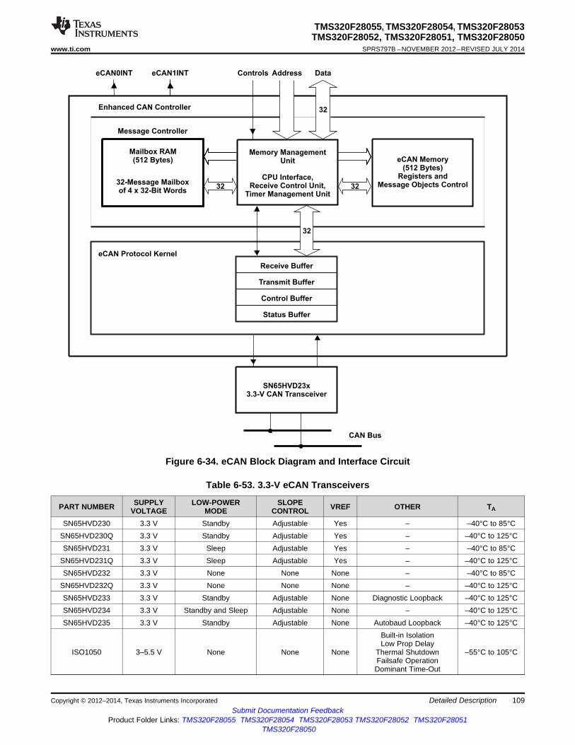
Mailbox RAM(512 Bytes)
32-Message Mailboxof 4 x 32-Bit Words
Memory ManagementUnit
CPU Interface,Receive Control Unit,
Timer Management Unit
eCAN Memory(512 Bytes)
Registers andMessage Objects Control
Message Controller
32 32
eCAN Protocol Kernel
Receive Buffer
Transmit Buffer
Control Buffer
Status Buffer
Enhanced CAN Controller 32
Controls Address DataeCAN1INTeCAN0INT
32
SN65HVD23x3.3-V CAN Transceiver
CAN Bus
TMS320F28055, TMS320F28054, TMS320F28053TMS320F28052, TMS320F28051, TMS320F28050
www.ti.com SPRS797B –NOVEMBER 2012–REVISED JULY 2014
Figure 6-34. eCAN Block Diagram and Interface Circuit
Table 6-53. 3.3-V eCAN Transceivers
SUPPLY LOW-POWER SLOPEPART NUMBER VREF OTHER TAVOLTAGE MODE CONTROLSN65HVD230 3.3 V Standby Adjustable Yes – –40°C to 85°C
SN65HVD230Q 3.3 V Standby Adjustable Yes – –40°C to 125°CSN65HVD231 3.3 V Sleep Adjustable Yes – –40°C to 85°C
SN65HVD231Q 3.3 V Sleep Adjustable Yes – –40°C to 125°CSN65HVD232 3.3 V None None None – –40°C to 85°C
SN65HVD232Q 3.3 V None None None – –40°C to 125°CSN65HVD233 3.3 V Standby Adjustable None Diagnostic Loopback –40°C to 125°CSN65HVD234 3.3 V Standby and Sleep Adjustable None – –40°C to 125°CSN65HVD235 3.3 V Standby Adjustable None Autobaud Loopback –40°C to 125°C
Built-in IsolationLow Prop Delay
ISO1050 3–5.5 V None None None Thermal Shutdown –55°C to 105°CFailsafe OperationDominant Time-Out
Copyright © 2012–2014, Texas Instruments Incorporated Detailed Description 109Submit Documentation Feedback
Product Folder Links: TMS320F28055 TMS320F28054 TMS320F28053 TMS320F28052 TMS320F28051TMS320F28050

Mailbox Enable - CANME
Mailbox Direction - CANMD
Transmission Request Set - CANTRS
Transmission Request Reset - CANTRR
Transmission Acknowledge - CANTA
Abort Acknowledge - CANAA
Received Message Pending - CANRMP
Received Message Lost - CANRML
Remote Frame Pending - CANRFP
Global Acceptance Mask - CANGAM
Master Control - CANMC
Bit-Timing Configuration - CANBTC
Error and Status - CANES
Transmit Error Counter - CANTEC
Receive Error Counter - CANREC
Global Interrupt Flag 0 - CANGIF0
Global Interrupt Mask - CANGIM
Mailbox Interrupt Mask - CANMIM
Mailbox Interrupt Level - CANMIL
Overwrite Protection Control - CANOPC
TX I/O Control - CANTIOC
RX I/O Control - CANRIOC
Time Stamp Counter - CANTSC
Global Interrupt Flag 1 - CANGIF1
Time-Out Control - CANTOC
Time-Out Status - CANTOS
Reserved
eCAN-A Control and Status Registers
Message Identifier - MSGID61E8h-61E9h
Message Control - MSGCTRL
Message Data Low - MDL
Message Data High - MDH
Message Mailbox (16 Bytes)
Control and Status Registers
6000h
603Fh
Local Acceptance Masks (LAM)(32 x 32-Bit RAM)
6040h
607Fh6080h
60BFh60C0h
60FFh
eCAN-A Memory (512 Bytes)
Message Object Time Stamps (MOTS)(32 x 32-Bit RAM)
Message Object Time-Out (MOTO)(32 x 32-Bit RAM)
Mailbox 06100h-6107h
Mailbox 16108h-610Fh
Mailbox 26110h-6117h
Mailbox 36118h-611Fh
eCAN-A Memory RAM (512 Bytes)
Mailbox 46120h-6127h
Mailbox 2861E0h-61E7h
Mailbox 2961E8h-61EFh
Mailbox 3061F0h-61F7h
Mailbox 3161F8h-61FFh
61EAh-61EBh
61ECh-61EDh
61EEh-61EFh
TMS320F28055, TMS320F28054, TMS320F28053TMS320F28052, TMS320F28051, TMS320F28050SPRS797B –NOVEMBER 2012–REVISED JULY 2014 www.ti.com
Figure 6-35. eCAN-A Memory Map
NOTEIf the eCAN module is not used in an application, the RAM available (LAM, MOTS, MOTO,and mailbox RAM) can be used as general-purpose RAM. The CAN module clock should beenabled if the eCAN RAM (LAM, MOTS, MOTO, and mailbox RAM) is used as general-purpose RAM.
110 Detailed Description Copyright © 2012–2014, Texas Instruments IncorporatedSubmit Documentation Feedback
Product Folder Links: TMS320F28055 TMS320F28054 TMS320F28053 TMS320F28052 TMS320F28051TMS320F28050
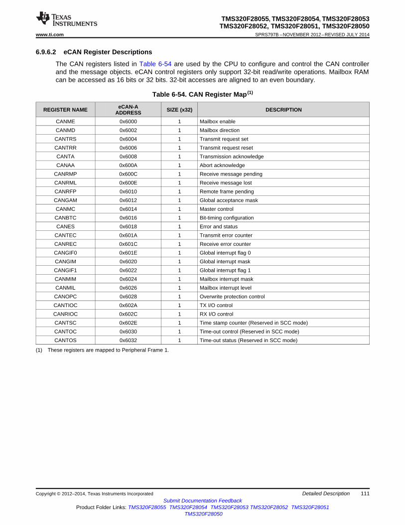
TMS320F28055, TMS320F28054, TMS320F28053TMS320F28052, TMS320F28051, TMS320F28050
www.ti.com SPRS797B –NOVEMBER 2012–REVISED JULY 2014
6.9.6.2 eCAN Register Descriptions
The CAN registers listed in Table 6-54 are used by the CPU to configure and control the CAN controllerand the message objects. eCAN control registers only support 32-bit read/write operations. Mailbox RAMcan be accessed as 16 bits or 32 bits. 32-bit accesses are aligned to an even boundary.
Table 6-54. CAN Register Map (1)
eCAN-AREGISTER NAME SIZE (x32) DESCRIPTIONADDRESSCANME 0x6000 1 Mailbox enableCANMD 0x6002 1 Mailbox directionCANTRS 0x6004 1 Transmit request setCANTRR 0x6006 1 Transmit request resetCANTA 0x6008 1 Transmission acknowledgeCANAA 0x600A 1 Abort acknowledge
CANRMP 0x600C 1 Receive message pendingCANRML 0x600E 1 Receive message lostCANRFP 0x6010 1 Remote frame pendingCANGAM 0x6012 1 Global acceptance maskCANMC 0x6014 1 Master controlCANBTC 0x6016 1 Bit-timing configurationCANES 0x6018 1 Error and status
CANTEC 0x601A 1 Transmit error counterCANREC 0x601C 1 Receive error counterCANGIF0 0x601E 1 Global interrupt flag 0CANGIM 0x6020 1 Global interrupt maskCANGIF1 0x6022 1 Global interrupt flag 1CANMIM 0x6024 1 Mailbox interrupt maskCANMIL 0x6026 1 Mailbox interrupt levelCANOPC 0x6028 1 Overwrite protection controlCANTIOC 0x602A 1 TX I/O controlCANRIOC 0x602C 1 RX I/O controlCANTSC 0x602E 1 Time stamp counter (Reserved in SCC mode)CANTOC 0x6030 1 Time-out control (Reserved in SCC mode)CANTOS 0x6032 1 Time-out status (Reserved in SCC mode)
(1) These registers are mapped to Peripheral Frame 1.
Copyright © 2012–2014, Texas Instruments Incorporated Detailed Description 111Submit Documentation Feedback
Product Folder Links: TMS320F28055 TMS320F28054 TMS320F28053 TMS320F28052 TMS320F28051TMS320F28050

TMS320F28055, TMS320F28054, TMS320F28053TMS320F28052, TMS320F28051, TMS320F28050SPRS797B –NOVEMBER 2012–REVISED JULY 2014 www.ti.com
6.9.7 Inter-Integrated Circuit
6.9.7.1 I2C Device-Specific Information
The device contains one I2C serial port. Figure 6-36 shows how the I2C peripheral module interfaceswithin the device.
The I2C module has the following features:• Compliance with the Philips Semiconductors I2C-bus specification (version 2.1):
– Support for 1-bit to 8-bit format transfers– 7-bit and 10-bit addressing modes– General call– START byte mode– Support for multiple master-transmitters and slave-receivers– Support for multiple slave-transmitters and master-receivers– Combined master transmit/receive and receive/transmit mode– Data transfer rate of from 10 kbps up to 400 kbps (I2C Fast-mode rate)
• One 4-word receive FIFO and one 4-word transmit FIFO• One interrupt that can be used by the CPU. This interrupt can be generated as a result of one of the
following conditions:– Transmit-data ready– Receive-data ready– Register-access ready– No-acknowledgment received– Arbitration lost– Stop condition detected– Addressed as slave
• An additional interrupt that can be used by the CPU when in FIFO mode• Module enable/disable capability• Free data format mode
112 Detailed Description Copyright © 2012–2014, Texas Instruments IncorporatedSubmit Documentation Feedback
Product Folder Links: TMS320F28055 TMS320F28054 TMS320F28053 TMS320F28052 TMS320F28051TMS320F28050

I2CXSR I2CDXR
I2CRSR I2CDRR
ClockSynchronizer
Prescaler
Noise Filters
Arbitrator
I2C INT
Peripheral Bus
Interrupt toCPU/PIE
SDA
SCL
Control/StatusRegisters CPU
I C Module2
TX FIFO
RX FIFO
FIFO Interrupt toCPU/PIE
TMS320F28055, TMS320F28054, TMS320F28053TMS320F28052, TMS320F28051, TMS320F28050
www.ti.com SPRS797B –NOVEMBER 2012–REVISED JULY 2014
A. The I2C registers are accessed at the SYSCLKOUT rate. The internal timing and signal waveforms of the I2C port arealso at the SYSCLKOUT rate.
B. The clock enable bit (I2CAENCLK) in the PCLKCRO register turns off the clock to the I2C port for low poweroperation. Upon reset, I2CAENCLK is clear, which indicates the peripheral internal clocks are off.
Figure 6-36. I2C Peripheral Module Interfaces
6.9.7.2 I2C Register Descriptions
The registers in Table 6-55 configure and control the I2C port operation.
Table 6-55. I2C-A Registers
EALLOWNAME ADDRESS DESCRIPTIONPROTECTEDI2COAR 0x7900 No I2C own address registerI2CIER 0x7901 No I2C interrupt enable registerI2CSTR 0x7902 No I2C status registerI2CCLKL 0x7903 No I2C clock low-time divider registerI2CCLKH 0x7904 No I2C clock high-time divider registerI2CCNT 0x7905 No I2C data count registerI2CDRR 0x7906 No I2C data receive registerI2CSAR 0x7907 No I2C slave address registerI2CDXR 0x7908 No I2C data transmit registerI2CMDR 0x7909 No I2C mode registerI2CISRC 0x790A No I2C interrupt source registerI2CPSC 0x790C No I2C prescaler registerI2CFFTX 0x7920 No I2C FIFO transmit registerI2CFFRX 0x7921 No I2C FIFO receive registerI2CRSR – No I2C receive shift register (not accessible to the CPU)I2CXSR – No I2C transmit shift register (not accessible to the CPU)
Copyright © 2012–2014, Texas Instruments Incorporated Detailed Description 113Submit Documentation Feedback
Product Folder Links: TMS320F28055 TMS320F28054 TMS320F28053 TMS320F28052 TMS320F28051TMS320F28050

TMS320F28055, TMS320F28054, TMS320F28053TMS320F28052, TMS320F28051, TMS320F28050SPRS797B –NOVEMBER 2012–REVISED JULY 2014 www.ti.com
6.9.7.3 I2C Electrical Data/Timing
Table 6-56. I2C Timing
TEST CONDITIONS MIN MAX UNITfSCL SCL clock frequency I2C clock module frequency is between 400 kHz
7 MHz and 12 MHz and I2C prescaler andclock divider registers are configuredappropriately
vil Low level input voltage 0.3 VDDIO VVih High level input voltage 0.7 VDDIO VVhys Input hysteresis 0.05 VDDIO VVol Low level output voltage 3 mA sink current 0 0.4 VtLOW Low period of SCL clock I2C clock module frequency is between 1.3 μs
7 MHz and 12 MHz and I2C prescaler andclock divider registers are configuredappropriately
tHIGH High period of SCL clock I2C clock module frequency is between 0.6 μs7 MHz and 12 MHz and I2C prescaler andclock divider registers are configuredappropriately
lI Input current with an input voltage –10 10 μAbetween 0.1 VDDIO and 0.9 VDDIO MAX
114 Detailed Description Copyright © 2012–2014, Texas Instruments IncorporatedSubmit Documentation Feedback
Product Folder Links: TMS320F28055 TMS320F28054 TMS320F28053 TMS320F28052 TMS320F28051TMS320F28050

EPWM1TZINT
PIE
EPWM1INT
EPWM2TZINT
EPWM2INT
EPWMxTZINT
EPWMxINT
CTRIPOutput
Subsystem
SOCA1
ADC SOCB1
SOCA2
SOCB2
SOCAx
SOCBx
EPWM1SYNCI
EPWM2SYNCI
EPWM1SYNCO
EPWM2SYNCO
EPWM1Module
EPWM2Module
EPWMxSYNCI
EPWMxModule
CTRIPxx
TZ6
TZ6
TZ1 TZ3to
TZ5CLOCKFAIL
TZ4EQEP1ERR
EMUSTOP
TZ5CLOCKFAIL
TZ4EQEP1ERR
EMUSTOP
EPWM1ENCLK
TBCLKSYNC
EPWM2ENCLK
TBCLKSYNC
TZ5
TZ6EPWMxENCLK
TBCLKSYNC
CLOCKFAILTZ4
EQEP1ERR
EMUSTOP
EPWM1B
C28x CPU
System Control
eQEP1
TZ1 TZ3to
TZ1 TZ3to
EPWM1SYNCO
EPWM2B
eCAPI
EPWMxB
EQEP1ERR
EPWMxA
EPWM2A
EPWM1A
GPIO
MUX
ADCSOCBO
ADCSOCAO
Pe
rip
he
ral
Bu
s
Pulse Stretch(32 SYSCLKOUT Cycles, Active-Low Output)
SOCA1SOCA2SPCAx
Pulse Stretch(32 SYSCLKOUT Cycles, Active-Low Output)
SOCB1SOCB2SPCBx
EPWMSYNCI
TMS320F28055, TMS320F28054, TMS320F28053TMS320F28052, TMS320F28051, TMS320F28050
www.ti.com SPRS797B –NOVEMBER 2012–REVISED JULY 2014
6.9.8 Enhanced Pulse Width Modulator
6.9.8.1 ePWM Device-Specific Information
The devices contain up to seven enhanced PWM modules (ePWM1–ePWM7). Figure 6-37 shows a blockdiagram of multiple ePWM modules. Figure 6-38 shows the signal interconnections with the ePWM. Seethe Enhanced Pulse Width Modulator (ePWM) Module chapter of the TMS320x2805x Piccolo TechnicalReference Manual (SPRUHE5) for more details.
Figure 6-37. ePWM
Copyright © 2012–2014, Texas Instruments Incorporated Detailed Description 115Submit Documentation Feedback
Product Folder Links: TMS320F28055 TMS320F28054 TMS320F28053 TMS320F28052 TMS320F28051TMS320F28050

TBPRD Shadow (24)
TBPRD Active (24)
CounterUp/Down(16 Bit)
TCBNTActive (16)
TBCTL[PHSEN]
CTR=PRD
16
PhaseControl
CTR=ZERO
CTR_Dir
CTR=ZERO
CTR=CMPB
Disabled
TBCTL[SYNCOSEL]
EPWMxSYNCO
Time-Base (TB)
TBPHS Active (24)
SyncIn/OutSelectMux
CTR=PRD
CTR=ZERO
CTR=CMPA
CTR=CMPB
CTR_Dir
DCAEVT1.soc(A)
DCBEVT1.soc(A)
EventTrigger
andInterrupt
(ET)
EPWMxINT
EPWMxSOCA
EPWMxSOCB
EPWMxSOCA
EPWMxSOCBADC
ActionQualifier
(AQ)
EPWMA
DeadBand(DB)
EPWMB
PWMChopper
(PC)
TripZone(TZ)
EPWMxA
EPWMxB
CTR=ZERO
EPWMxTZINT
TZ1 TZ3to
EMUSTOP
CLOCKFAIL
EQEP1ERR
DCAEVT1.force(A)
DCAEVT2.force(A)
DCBEVT1.force(A)
DCBEVT2.force(A)
CTR=CMPA
16
CTR=CMPB
16
CMPB Active (16)
CMPB Shadow (16)
CTR=PRD or ZERO
DCAEVT1.interDCBEVT1.inter
DCAEVT2.inter
DCBEVT2.inter
EPWMxSYNCI
TBCTL[SWFSYNC](Software ForcedSync)
DCAEVT1.syncDCBEVT1.sync
CMPA Active (24)
CMPA Shadow (24)
TMS320F28055, TMS320F28054, TMS320F28053TMS320F28052, TMS320F28051, TMS320F28050SPRS797B –NOVEMBER 2012–REVISED JULY 2014 www.ti.com
A. These events are generated by the Type 1 ePWM digital compare (DC) submodule based on the levels of theCOMPxOUT and TZ signals.
Figure 6-38. ePWM Sub-Modules Showing Critical Internal Signal Interconnections
116 Detailed Description Copyright © 2012–2014, Texas Instruments IncorporatedSubmit Documentation Feedback
Product Folder Links: TMS320F28055 TMS320F28054 TMS320F28053 TMS320F28052 TMS320F28051TMS320F28050

TMS320F28055, TMS320F28054, TMS320F28053TMS320F28052, TMS320F28051, TMS320F28050
www.ti.com SPRS797B –NOVEMBER 2012–REVISED JULY 2014
6.9.8.2 ePWM Register Descriptions
Table 6-57 and Table 6-58 show the complete ePWM register set per module.
Table 6-57. ePWM1–ePWM4 Control and Status Registers
SIZE (x16) /NAME ePWM1 ePWM2 ePWM3 ePWM4 DESCRIPTION#SHADOWTBCTL 0x6800 0x6840 0x6880 0x68C0 1 / 0 Time Base Control RegisterTBSTS 0x6801 0x6841 0x6881 0x68C1 1 / 0 Time Base Status RegisterReserved 0x6802 0x6842 0x6882 0x68C2 1 / 0 ReservedTBPHS 0x6803 0x6843 0x6883 0x68C3 1 / 0 Time Base Phase RegisterTBCTR 0x6804 0x6844 0x6884 0x68C4 1 / 0 Time Base Counter RegisterTBPRD 0x6805 0x6845 0x6885 0x68C5 1 / 1 Time Base Period Register SetReserved 0x6806 0x6846 0x6886 0x68C6 1 / 1 ReservedCMPCTL 0x6807 0x6847 0x6887 0x68C7 1 / 0 Counter Compare Control RegisterReserved 0x6808 0x6848 0x6888 0x68C8 1 / 1 ReservedCMPA 0x6809 0x6849 0x6889 0x68C9 1 / 1 Counter Compare A Register SetCMPB 0x680A 0x684A 0x688A 0x68CA 1 / 1 Counter Compare B Register SetAQCTLA 0x680B 0x684B 0x688B 0x68CB 1 / 0 Action Qualifier Control Register For Output AAQCTLB 0x680C 0x684C 0x688C 0x68CC 1 / 0 Action Qualifier Control Register For Output BAQSFRC 0x680D 0x684D 0x688D 0x68CD 1 / 0 Action Qualifier Software Force RegisterAQCSFRC 0x680E 0x684E 0x688E 0x68CE 1 / 1 Action Qualifier Continuous S/W Force Register SetDBCTL 0x680F 0x684F 0x688F 0x68CF 1 / 1 Dead-Band Generator Control RegisterDBRED 0x6810 0x6850 0x6890 0x68D0 1 / 0 Dead-Band Generator Rising Edge Delay Count RegisterDBFED 0x6811 0x6851 0x6891 0x68D1 1 / 0 Dead-Band Generator Falling Edge Delay Count RegisterTZSEL 0x6812 0x6852 0x6892 0x68D2 1 / 0 Trip Zone Select Register (1)
TZDCSEL 0x6813 0x6853 0x6893 0x98D3 1 / 0 Trip Zone Digital Compare RegisterTZCTL 0x6814 0x6854 0x6894 0x68D4 1 / 0 Trip Zone Control Register (1)
TZEINT 0x6815 0x6855 0x6895 0x68D5 1 / 0 Trip Zone Enable Interrupt Register (1)
TZFLG 0x6816 0x6856 0x6896 0x68D6 1 / 0 Trip Zone Flag Register (1)
TZCLR 0x6817 0x6857 0x6897 0x68D7 1 / 0 Trip Zone Clear Register (1)
TZFRC 0x6818 0x6858 0x6898 0x68D8 1 / 0 Trip Zone Force Register (1)
ETSEL 0x6819 0x6859 0x6899 0x68D9 1 / 0 Event Trigger Selection RegisterETPS 0x681A 0x685A 0x689A 0x68DA 1 / 0 Event Trigger Prescale RegisterETFLG 0x681B 0x685B 0x689B 0x68DB 1 / 0 Event Trigger Flag RegisterETCLR 0x681C 0x685C 0x689C 0x68DC 1 / 0 Event Trigger Clear Register
(1) Registers that are EALLOW protected.
Copyright © 2012–2014, Texas Instruments Incorporated Detailed Description 117Submit Documentation Feedback
Product Folder Links: TMS320F28055 TMS320F28054 TMS320F28053 TMS320F28052 TMS320F28051TMS320F28050

TMS320F28055, TMS320F28054, TMS320F28053TMS320F28052, TMS320F28051, TMS320F28050SPRS797B –NOVEMBER 2012–REVISED JULY 2014 www.ti.com
Table 6-57. ePWM1–ePWM4 Control and Status Registers (continued)SIZE (x16) /NAME ePWM1 ePWM2 ePWM3 ePWM4 DESCRIPTION#SHADOW
ETFRC 0x681D 0x685D 0x689D 0x68DD 1 / 0 Event Trigger Force RegisterPCCTL 0x681E 0x685E 0x689E 0x68DE 1 / 0 PWM Chopper Control RegisterReserved 0x6820 0x6860 0x68A0 0x68E0 1 / 0 ReservedReserved 0x6821 - - - 1 / 0 ReservedReserved 0x6826 - - - 1 / 0 ReservedReserved 0x6828 0x6868 0x68A8 0x68E8 1 / 0 ReservedReserved 0x682A 0x686A 0x68AA 0x68EA 1 / W (2) ReservedTBPRDM 0x682B 0x686B 0x68AB 0x68EB 1 / W (2) Time Base Period Register MirrorReserved 0x682C 0x686C 0x68AC 0x68EC 1 / W (2) ReservedCMPAM 0x682D 0x686D 0x68AD 0x68ED 1 / W (2) Compare A Register MirrorDCTRIPSEL 0x6830 0x6870 0x68B0 0x68F0 1 / 0 Digital Compare Trip Select Register (1)
DCACTL 0x6831 0x6871 0x68B1 0x68F1 1 / 0 Digital Compare A Control Register (1)
DCBCTL 0x6832 0x6872 0x68B2 0x68F2 1 / 0 Digital Compare B Control Register (1)
DCFCTL 0x6833 0x6873 0x68B3 0x68F3 1 / 0 Digital Compare Filter Control Register (1)
DCCAPCT 0x6834 0x6874 0x68B4 0x68F4 1 / 0 Digital Compare Capture Control Register (3)
DCFOFFSET 0x6835 0x6875 0x68B5 0x68F5 1 / 1 Digital Compare Filter Offset RegisterDCFOFFSETCNT 0x6836 0x6876 0x68B6 0x68F6 1 / 0 Digital Compare Filter Offset Counter RegisterDCFWINDOW 0x6837 0x6877 0x68B7 0x68F7 1 / 0 Digital Compare Filter Window RegisterDCFWINDOWCNT 0x6838 0x6878 0x68B8 0x68F8 1 / 0 Digital Compare Filter Window Counter RegisterDCCAP 0x6839 0x6879 0x68B9 0x68F9 1 / 1 Digital Compare Counter Capture Register
(2) W = Write to shadow register(3) Registers that are EALLOW protected.
118 Detailed Description Copyright © 2012–2014, Texas Instruments IncorporatedSubmit Documentation Feedback
Product Folder Links: TMS320F28055 TMS320F28054 TMS320F28053 TMS320F28052 TMS320F28051TMS320F28050

TMS320F28055, TMS320F28054, TMS320F28053TMS320F28052, TMS320F28051, TMS320F28050
www.ti.com SPRS797B –NOVEMBER 2012–REVISED JULY 2014
Table 6-58. ePWM5–ePWM7 Control and Status Registers
SIZE (x16) /NAME ePWM5 ePWM6 ePWM7 DESCRIPTION#SHADOWTBCTL 0x6900 0x6940 0x6980 1 / 0 Time Base Control RegisterTBSTS 0x6901 0x6941 0x6981 1 / 0 Time Base Status RegisterReserved 0x6902 0x6942 0x6982 1 / 0 ReservedTBPHS 0x6903 0x6943 0x6983 1 / 0 Time Base Phase RegisterTBCTR 0x6904 0x6944 0x6984 1 / 0 Time Base Counter RegisterTBPRD 0x6905 0x6945 0x6985 1 / 1 Time Base Period Register SetReserved 0x6906 0x6946 0x6986 1 / 1 ReservedCMPCTL 0x6907 0x6947 0x6987 1 / 0 Counter Compare Control RegisterReserved 0x6908 0x6948 0x6988 1 / 1 ReservedCMPA 0x6909 0x6949 0x6989 1 / 1 Counter Compare A Register SetCMPB 0x690A 0x694A 0x698A 1 / 1 Counter Compare B Register SetAQCTLA 0x690B 0x694B 0x698B 1 / 0 Action Qualifier Control Register For Output AAQCTLB 0x690C 0x694C 0x698C 1 / 0 Action Qualifier Control Register For Output BAQSFRC 0x690D 0x694D 0x698D 1 / 0 Action Qualifier Software Force RegisterAQCSFRC 0x690E 0x694E 0x698E 1 / 1 Action Qualifier Continuous S/W Force Register SetDBCTL 0x690F 0x694F 0x698F 1 / 1 Dead-Band Generator Control Register
Dead-Band Generator Rising Edge Delay CountDBRED 0x6910 0x6950 0x6990 1 / 0 RegisterDead-Band Generator Falling Edge Delay CountDBFED 0x6911 0x6951 0x6991 1 / 0 Register
TZSEL 0x6912 0x6952 0x6992 1 / 0 Trip Zone Select Register (1)
TZDCSEL 0x6913 0x6953 0x6993 1 / 0 Trip Zone Digital Compare RegisterTZCTL 0x6914 0x6954 0x6994 1 / 0 Trip Zone Control Register (1)
TZEINT 0x6915 0x6955 0x6995 1 / 0 Trip Zone Enable Interrupt Register (1)
TZFLG 0x6916 0x6956 0x6996 1 / 0 Trip Zone Flag Register (1)
TZCLR 0x6917 0x6957 0x6997 1 / 0 Trip Zone Clear Register (1)
TZFRC 0x6918 0x6958 0x6998 1 / 0 Trip Zone Force Register (1)
ETSEL 0x6919 0x6959 0x6999 1 / 0 Event Trigger Selection RegisterETPS 0x691A 0x695A 0x699A 1 / 0 Event Trigger Prescale RegisterETFLG 0x691B 0x695B 0x699B 1 / 0 Event Trigger Flag RegisterETCLR 0x691C 0x695C 0x699C 1 / 0 Event Trigger Clear RegisterETFRC 0x691D 0x695D 0x699D 1 / 0 Event Trigger Force RegisterPCCTL 0x691E 0x695E 0x699E 1 / 0 PWM Chopper Control RegisterReserved 0x6920 0x6960 0x69A0 1 / 0 ReservedReserved - - - 1 / 0 ReservedReserved - - - 1 / 0 ReservedReserved 0x6928 0x6968 0x69A8 1 / 0 ReservedReserved 0x692A 0x696A 0x69AA 1 / W (2) ReservedTBPRDM 0x692B 0x696B 0x69AB 1 / W (2) Time Base Period Register MirrorReserved 0x692C 0x696C 0x69AC 1 / W (2) ReservedCMPAM 0x692D 0x696D 0x69AD 1 / W (2) Compare A Register MirrorDCTRIPSEL 0x6930 0x6970 0x69B0 1 / 0 Digital Compare Trip Select Register (1)
DCACTL 0x6931 0x6971 0x69B1 1 / 0 Digital Compare A Control Register (1)
DCBCTL 0x6932 0x6972 0x69B2 1 / 0 Digital Compare B Control Register (1)
DCFCTL 0x6933 0x6973 0x69B3 1 / 0 Digital Compare Filter Control Register (1)
DCCAPCT 0x6934 0x6974 0x69B4 1 / 0 Digital Compare Capture Control Register (1)
(1) Registers that are EALLOW protected.(2) W = Write to shadow register
Copyright © 2012–2014, Texas Instruments Incorporated Detailed Description 119Submit Documentation Feedback
Product Folder Links: TMS320F28055 TMS320F28054 TMS320F28053 TMS320F28052 TMS320F28051TMS320F28050

TMS320F28055, TMS320F28054, TMS320F28053TMS320F28052, TMS320F28051, TMS320F28050SPRS797B –NOVEMBER 2012–REVISED JULY 2014 www.ti.com
Table 6-58. ePWM5–ePWM7 Control and Status Registers (continued)SIZE (x16) /NAME ePWM5 ePWM6 ePWM7 DESCRIPTION#SHADOW
DCFOFFSET 0x6935 0x6975 0x69B5 1 / 1 Digital Compare Filter Offset RegisterDCFOFFSETCNT 0x6936 0x6976 0x69B6 1 / 0 Digital Compare Filter Offset Counter RegisterDCFWINDOW 0x6937 0x6977 0x69B7 1 / 0 Digital Compare Filter Window RegisterDCFWINDOWCNT 0x6938 0x6978 0x69B8 1 / 0 Digital Compare Filter Window Counter RegisterDCCAP 0x6939 0x6979 0x69B9 1 / 1 Digital Compare Counter Capture Register
6.9.8.3 ePWM Electrical Data/Timing
PWM refers to PWM outputs on ePWM1–ePWM7. Table 6-59 shows the PWM timing requirements andTable 6-60, switching characteristics.
Table 6-59. ePWM Timing Requirements (1)
MIN MAX UNITAsynchronous 2tc(SCO) cycles
tw(SYCIN) Sync input pulse width Synchronous 2tc(SCO) cyclesWith input qualifier 1tc(SCO) + tw(IQSW) cycles
(1) For an explanation of the input qualifier parameters, see Table 6-72.
Table 6-60. ePWM Switching Characteristicsover recommended operating conditions (unless otherwise noted)
PARAMETER TEST CONDITIONS MIN MAX UNITtw(PWM) Pulse duration, PWMx output high/low 33.33 nstw(SYNCOUT) Sync output pulse width 8tc(SCO) cycles
Delay time, trip input active to PWM forced hightd(PWM)tza no pin load 25 nsDelay time, trip input active to PWM forced lowtd(TZ-PWM)HZ Delay time, trip input active to PWM Hi-Z 20 ns
120 Detailed Description Copyright © 2012–2014, Texas Instruments IncorporatedSubmit Documentation Feedback
Product Folder Links: TMS320F28055 TMS320F28054 TMS320F28053 TMS320F28052 TMS320F28051TMS320F28050

PWM(B)
TZ(A)
SYSCLK
tw(TZ)
td(TZ-PWM)HZ
TMS320F28055, TMS320F28054, TMS320F28053TMS320F28052, TMS320F28051, TMS320F28050
www.ti.com SPRS797B –NOVEMBER 2012–REVISED JULY 2014
6.9.8.3.1 Trip-Zone Input Timing
Table 6-61. Trip-Zone Input Timing Requirements (1)
MIN MAX UNITAsynchronous 2tc(TBCLK) cycles
tw(TZ) Pulse duration, TZx input low Synchronous 2tc(TBCLK) cyclesWith input qualifier 2tc(TBCLK) + tw(IQSW) cycles
(1) For an explanation of the input qualifier parameters, see Table 6-72.
A. TZ - TZ1, TZ2, TZ3, TZ4, TZ5, TZ6B. PWM refers to all the PWM pins in the device. The state of the PWM pins after TZ is taken high depends on the PWM
recovery software.
Figure 6-39. PWM Hi-Z Characteristics
Copyright © 2012–2014, Texas Instruments Incorporated Detailed Description 121Submit Documentation Feedback
Product Folder Links: TMS320F28055 TMS320F28054 TMS320F28053 TMS320F28052 TMS320F28051TMS320F28050

TSCTR(counter−32 bit)
RST
CAP1(APRD active)
LD
CAP2(ACMP active)
LD
CAP3(APRD shadow)
LD
CAP4(ACMP shadow)
LD
Continuous /Oneshot
Capture Control
LD1
LD2
LD3
LD4
32
32
PRD [0−31]
CMP [0−31]
CTR [0−31]
eCAPx
InterruptTrigger
andFlag
control
to PIE
CTR=CMP
32
32
32
32
32
ACMPshadow
Event
Pre-scale
CTRPHS(phase register−32 bit)
SYNCOut
SYNCIn
Eventqualifier
Polarityselect
Polarityselect
Polarityselect
Polarityselect
CTR=PRD
CTR_OVF
4
PWMcompare
logic
CTR [0−31]
PRD [0−31]
CMP [0−31]
CTR=CMP
CTR=PRD
CTR_OVFOVF
APWM mode
Delta−mode
SY
NC
4Capture events
CEVT[1:4]
APRDshadow
32
32 MO
DE
SE
LE
CT
TMS320F28055, TMS320F28054, TMS320F28053TMS320F28052, TMS320F28051, TMS320F28050SPRS797B –NOVEMBER 2012–REVISED JULY 2014 www.ti.com
6.9.9 Enhanced Capture Module
6.9.9.1 eCAP Module Device-Specific Information
The device contains an enhanced capture module (eCAP1). Figure 6-40 shows a functional block diagramof a module.
Figure 6-40. eCAP Functional Block Diagram
The eCAP module is clocked at the SYSCLKOUT rate.
The clock enable bits (ECAP1 ENCLK) in the PCLKCR1 register turn off the eCAP module individually (forlow power operation). Upon reset, ECAP1ENCLK is set to low, indicating that the peripheral clock is off.
122 Detailed Description Copyright © 2012–2014, Texas Instruments IncorporatedSubmit Documentation Feedback
Product Folder Links: TMS320F28055 TMS320F28054 TMS320F28053 TMS320F28052 TMS320F28051TMS320F28050

TMS320F28055, TMS320F28054, TMS320F28053TMS320F28052, TMS320F28051, TMS320F28050
www.ti.com SPRS797B –NOVEMBER 2012–REVISED JULY 2014
6.9.9.2 eCAP Module Register Descriptions
Table 6-62 shows the eCAP Control and Status Registers.
Table 6-62. eCAP Control and Status Registers
NAME eCAP1 SIZE (x16) EALLOW PROTECTED DESCRIPTIONTSCTR 0x6A00 2 Time-Stamp Counter
CTRPHS 0x6A02 2 Counter Phase Offset Value RegisterCAP1 0x6A04 2 Capture 1 RegisterCAP2 0x6A06 2 Capture 2 RegisterCAP3 0x6A08 2 Capture 3 RegisterCAP4 0x6A0A 2 Capture 4 Register
Reserved 0x6A0C – 0x6A12 8 ReservedECCTL1 0x6A14 1 Capture Control Register 1ECCTL2 0x6A15 1 Capture Control Register 2ECEINT 0x6A16 1 Capture Interrupt Enable RegisterECFLG 0x6A17 1 Capture Interrupt Flag RegisterECCLR 0x6A18 1 Capture Interrupt Clear RegisterECFRC 0x6A19 1 Capture Interrupt Force Register
Reserved 0x6A1A – 0x6A1F 6 Reserved
6.9.9.3 eCAP Module Electrical Data/Timing
Table 6-63 shows the eCAP timing requirement and Table 6-64 shows the eCAP switching characteristics.
Table 6-63. eCAP Timing Requirement (1)
MIN MAX UNITAsynchronous 2tc(SCO) cycles
tw(CAP) Capture input pulse width Synchronous 2tc(SCO) cyclesWith input qualifier 1tc(SCO) + tw(IQSW) cycles
(1) For an explanation of the input qualifier parameters, see Table 6-72.
Table 6-64. eCAP Switching Characteristicsover recommended operating conditions (unless otherwise noted)
PARAMETER MIN MAX UNITtw(APWM) Pulse duration, APWMx output high/low 20 ns
Copyright © 2012–2014, Texas Instruments Incorporated Detailed Description 123Submit Documentation Feedback
Product Folder Links: TMS320F28055 TMS320F28054 TMS320F28053 TMS320F28052 TMS320F28051TMS320F28050

QWDTMR
QWDPRD
16
QWDOGUTIME
QUPRD
QUTMR
32
UTOUT
WDTOUT
QuadratureCapture
Unit(QCAP)
QCPRDLAT
QCTMRLAT
16
QFLG
QEPSTS
QEPCTL
RegistersUsed by
Multiple Units
QCLK
QDIR
QI
QS
PHE
PCSOUT
QuadratureDecoder
(QDU)
QDECCTL
16
Position Counter/Control Unit
(PCCU)QPOSLAT
QPOSSLAT
16
QPOSILAT
EQEPxAIN
EQEPxBIN
EQEPxIIN
EQEPxIOUT
EQEPxIOE
EQEPxSIN
EQEPxSOUT
EQEPxSOE
GPIOMUX
EQEPxA/XCLK
EQEPxB/XDIR
EQEPxS
EQEPxI
QPOSCMP QEINT
QFRC
32
QCLR
QPOSCTL
1632
QPOSCNT
QPOSMAX
QPOSINIT
PIEEQEPxINT
eQEP Peripheral
System ControlRegisters
QCTMR
QCPRD
1616
QCAPCTL
EQEPxENCLK
SYSCLKOUT
To CPU
Da
ta B
us
TMS320F28055, TMS320F28054, TMS320F28053TMS320F28052, TMS320F28051, TMS320F28050SPRS797B –NOVEMBER 2012–REVISED JULY 2014 www.ti.com
6.9.10 Enhanced Quadrature Encoder Pulse
6.9.10.1 eQEP Device-Specific Information
The device contains one eQEP module. Figure 6-41 shows the eQEP functional block diagram.
Figure 6-41. eQEP Functional Block Diagram
124 Detailed Description Copyright © 2012–2014, Texas Instruments IncorporatedSubmit Documentation Feedback
Product Folder Links: TMS320F28055 TMS320F28054 TMS320F28053 TMS320F28052 TMS320F28051TMS320F28050

TMS320F28055, TMS320F28054, TMS320F28053TMS320F28052, TMS320F28051, TMS320F28050
www.ti.com SPRS797B –NOVEMBER 2012–REVISED JULY 2014
6.9.10.2 eQEP Register Descriptions
Table 6-65 shows the eQEP Control and Status Registers.
Table 6-65. eQEP Control and Status Registers
eQEP1eQEP1NAME SIZE(x16)/ REGISTER DESCRIPTIONADDRESS #SHADOWQPOSCNT 0x6B00 2/0 eQEP Position CounterQPOSINIT 0x6B02 2/0 eQEP Initialization Position CountQPOSMAX 0x6B04 2/0 eQEP Maximum Position CountQPOSCMP 0x6B06 2/1 eQEP Position-compareQPOSILAT 0x6B08 2/0 eQEP Index Position LatchQPOSSLAT 0x6B0A 2/0 eQEP Strobe Position LatchQPOSLAT 0x6B0C 2/0 eQEP Position LatchQUTMR 0x6B0E 2/0 eQEP Unit TimerQUPRD 0x6B10 2/0 eQEP Unit Period RegisterQWDTMR 0x6B12 1/0 eQEP Watchdog TimerQWDPRD 0x6B13 1/0 eQEP Watchdog Period RegisterQDECCTL 0x6B14 1/0 eQEP Decoder Control RegisterQEPCTL 0x6B15 1/0 eQEP Control RegisterQCAPCTL 0x6B16 1/0 eQEP Capture Control RegisterQPOSCTL 0x6B17 1/0 eQEP Position-compare Control RegisterQEINT 0x6B18 1/0 eQEP Interrupt Enable RegisterQFLG 0x6B19 1/0 eQEP Interrupt Flag RegisterQCLR 0x6B1A 1/0 eQEP Interrupt Clear RegisterQFRC 0x6B1B 1/0 eQEP Interrupt Force RegisterQEPSTS 0x6B1C 1/0 eQEP Status RegisterQCTMR 0x6B1D 1/0 eQEP Capture TimerQCPRD 0x6B1E 1/0 eQEP Capture Period RegisterQCTMRLAT 0x6B1F 1/0 eQEP Capture Timer LatchQCPRDLAT 0x6B20 1/0 eQEP Capture Period Latch
0x6B21 –Reserved 31/00x6B3F
Copyright © 2012–2014, Texas Instruments Incorporated Detailed Description 125Submit Documentation Feedback
Product Folder Links: TMS320F28055 TMS320F28054 TMS320F28053 TMS320F28052 TMS320F28051TMS320F28050

TMS320F28055, TMS320F28054, TMS320F28053TMS320F28052, TMS320F28051, TMS320F28050SPRS797B –NOVEMBER 2012–REVISED JULY 2014 www.ti.com
6.9.10.3 eQEP Electrical Data/Timing
Table 6-66 shows the eQEP timing requirement and Table 6-67 shows the eQEP switchingcharacteristics.
Table 6-66. eQEP Timing Requirements (1)
TEST CONDITIONS MIN MAX UNITtw(QEPP) QEP input period Synchronous 2tc(SCO) cycles
With input qualifier 2[1tc(SCO) + tw(IQSW)] cyclestw(INDEXH) QEP Index Input High time Synchronous 2tc(SCO) cycles
With input qualifier 2tc(SCO) +tw(IQSW) cyclestw(INDEXL) QEP Index Input Low time Synchronous 2tc(SCO) cycles
With input qualifier 2tc(SCO) + tw(IQSW) cyclestw(STROBH) QEP Strobe High time Synchronous 2tc(SCO) cycles
With input qualifier 2tc(SCO) + tw(IQSW) cyclestw(STROBL) QEP Strobe Input Low time Synchronous 2tc(SCO) cycles
With input qualifier 2tc(SCO) +tw(IQSW) cycles
(1) For an explanation of the input qualifier parameters, see Table 6-72.
Table 6-67. eQEP Switching Characteristicsover recommended operating conditions (unless otherwise noted)
PARAMETER MIN MAX UNITtd(CNTR)xin Delay time, external clock to counter increment 4tc(SCO) cyclestd(PCS-OUT)QEP Delay time, QEP input edge to position compare sync output 6tc(SCO) cycles
126 Detailed Description Copyright © 2012–2014, Texas Instruments IncorporatedSubmit Documentation Feedback
Product Folder Links: TMS320F28055 TMS320F28054 TMS320F28053 TMS320F28052 TMS320F28051TMS320F28050

TRST
1
0
C28xCore
TCK/GPIO38
TCK
XCLKIN
GPIO38_in
GPIO38_out
TDO
GPIO37_out
TDO/GPIO37
GPIO37_in
1
0
TMSTMS/GPIO36
GPIO36_out
GPIO36_in
1
1
0
TDITDI/GPIO35
GPIO35_out
GPIO35_in
1
TRSTTRST
= 0: JTAG Disabled (GPIO Mode)= 1: JTAG Mode
TRST
TMS320F28055, TMS320F28054, TMS320F28053TMS320F28052, TMS320F28051, TMS320F28050
www.ti.com SPRS797B –NOVEMBER 2012–REVISED JULY 2014
6.9.11 JTAG Port
6.9.11.1 JTAG Port Device-Specific Information
On the 2805x device, the JTAG port is reduced to 5 pins (TRST, TCK, TDI, TMS, TDO). TCK, TDI, TMSand TDO pins are also GPIO pins. The TRST signal selects either JTAG or GPIO operating mode for thepins in Figure 6-42. During emulation/debug, the GPIO function of these pins are not available. If theGPIO38/TCK/XCLKIN pin is used to provide an external clock, an alternate clock source should be usedto clock the device during emulation/debug since this pin will be needed for the TCK function.
NOTEIn 2805x devices, the JTAG pins may also be used as GPIO pins. Care should be taken inthe board design to ensure that the circuitry connected to these pins do not affect theemulation capabilities of the JTAG pin function. Any circuitry connected to these pins shouldnot prevent the emulator from driving (or being driven by) the JTAG pins for successfuldebug.
Figure 6-42. JTAG/GPIO Multiplexing
Copyright © 2012–2014, Texas Instruments Incorporated Detailed Description 127Submit Documentation Feedback
Product Folder Links: TMS320F28055 TMS320F28054 TMS320F28053 TMS320F28052 TMS320F28051TMS320F28050

TMS320F28055, TMS320F28054, TMS320F28053TMS320F28052, TMS320F28051, TMS320F28050SPRS797B –NOVEMBER 2012–REVISED JULY 2014 www.ti.com
6.9.12 General-Purpose Input/Output
6.9.12.1 GPIO Device-Specific Information
The GPIO MUX can multiplex up to three independent peripheral signals on a single GPIO pin in additionto providing individual pin bit-banging I/O capability.
Table 6-68. GPIOA MUX (1) (2)
DEFAULT AT RESET PERIPHERAL PERIPHERAL PERIPHERALPRIMARY I/O SELECTION 1 SELECTION 2 SELECTION 3FUNCTIONGPAMUX1 REGISTER (GPAMUX1 BITS = 00) (GPAMUX1 BITS = 01) (GPAMUX1 BITS = 10) (GPAMUX1 BITS = 11)BITS
1-0 GPIO0 EPWM1A (O) Reserved Reserved3-2 GPIO1 EPWM1B (O) Reserved CTRIPM1OUT (O)5-4 GPIO2 EPWM2A (O) Reserved Reserved7-6 GPIO3 EPWM2B (O) SPISOMIA (I/O) Reserved9-8 GPIO4 EPWM3A (O) Reserved Reserved
11-10 GPIO5 EPWM3B (O) SPISIMOA (I/O) ECAP1 (I/O)13-12 GPIO6 EPWM4A (O) EPWMSYNCI (I) EPWMSYNCO (O)15-14 GPIO7 EPWM4B (O) SCIRXDA (I) Reserved17-16 GPIO8 EPWM5A (O) Reserved ADCSOCAO (O)19-18 GPIO9 EPWM5B (O) SCITXDB (O) Reserved21-20 GPIO10 EPWM6A (O) Reserved ADCSOCBO (O)23-22 GPIO11 EPWM6B (O) SCIRXDB (I) Reserved
TZ1 (I)/25-24 GPIO12 SCITXDA (O) ReservedCTRIPM1OUT (O)27-26 GPIO13 TZ2 (I) Reserved Reserved
TZ3 (I)/29-28 GPIO14 SCITXDB (O) ReservedCTRIPPFCOUT (O)TZ1 (I)/31-30 GPIO15 SCIRXDB (I) ReservedCTRIPM1OUT (O)
(1) The word reserved means that there is no peripheral assigned to this GPxMUX1/2 register setting. Should the Reserved GPxMUX1/2register setting be selected, the state of the pin will be undefined and the pin may be driven. This selection is a reserved configurationfor future expansion.
(2) I = Input, O = Output, OC = Open Collector, OD = Open Drain
128 Detailed Description Copyright © 2012–2014, Texas Instruments IncorporatedSubmit Documentation Feedback
Product Folder Links: TMS320F28055 TMS320F28054 TMS320F28053 TMS320F28052 TMS320F28051TMS320F28050

TMS320F28055, TMS320F28054, TMS320F28053TMS320F28052, TMS320F28051, TMS320F28050
www.ti.com SPRS797B –NOVEMBER 2012–REVISED JULY 2014
Table 6-68. GPIOA MUX(1) (2) (continued)DEFAULT AT RESET PERIPHERAL PERIPHERAL PERIPHERALPRIMARY I/O SELECTION 1 SELECTION 2 SELECTION 3FUNCTION
GPAMUX2 REGISTER (GPAMUX2 BITS = 00) (GPAMUX2 BITS = 01) (GPAMUX2 BITS = 10) (GPAMUX2 BITS = 11)BITS1-0 GPIO16 SPISIMOA (I/O) EQEP1S (I/O) TZ2 (I)
TZ3 (I)/3-2 GPIO17 SPISOMIA (I/O) EQEP1I (I/O) CTRIPPFCOUT (O)5-4 GPIO18 SPICLKA (I/O) SCITXDB (O) XCLKOUT (O)7-6 GPIO19/XCLKIN SPISTEA (I/O) SCIRXDB (I) ECAP1 (I/O)9-8 GPIO20 EQEP1A (I) EPWM7A (O) CTRIPM1OUT (O)
11-10 GPIO21 EQEP1B (I) EPWM7B (O) Reserved13-12 GPIO22 EQEP1S (I/O) Reserved SCITXDB (O)15-14 GPIO23 EQEP1I (I/O) Reserved SCIRXDB (I)17-16 GPIO24 ECAP1 (I/O) EPWM7A (O) Reserved19-18 GPIO25 Reserved Reserved Reserved21-20 GPIO26 Reserved SCIRXDC (O) Reserved23-22 GPIO27 Reserved SCITXDC (O) Reserved25-24 GPIO28 SCIRXDA (I) SDAA (I/OC) TZ2 (I)
TZ3 (I)/27-26 GPIO29 SCITXDA (O) SCLA (I/OC) CTRIPPFCOUT (O)29-28 GPIO30 CANRXA (I) SCIRXDB (I) EPWM7A (O)31-30 GPIO31 CANTXA (O) SCITXDB (I) EPWM7B (O)
Table 6-69. GPIOB MUX (1)
DEFAULT AT RESET PERIPHERAL PERIPHERAL PERIPHERALPRIMARY I/O FUNCTION SELECTION 1 SELECTION 2 SELECTION 3
GPBMUX1 REGISTER (GPBMUX1 BITS = 00) (GPBMUX1 BITS = 01) (GPBMUX1 BITS = 10) (GPBMUX1 BITS = 11)BITS1-0 GPIO32 SDAA (I/OC) EPWMSYNCI (I) EQEP1S (I/O)3-2 GPIO33 SCLA (I/OC) EPWMSYNCO (O) EQEP1I (I/O)5-4 GPIO34 Reserved Reserved CTRIPPFCOUT (O)7-6 GPIO35 (TDI) Reserved Reserved Reserved9-8 GPIO36 (TMS) Reserved Reserved Reserved
11-10 GPIO37 (TDO) Reserved Reserved Reserved13-12 GPIO38/XCLKIN (TCK) Reserved Reserved Reserved15-14 GPIO39 Reserved SCIRXDC (I) CTRIPPFCOUT (O)17-16 GPIO40 EPWM7A (O) Reserved Reserved19-18 Reserved Reserved Reserved Reserved21-20 GPIO42 Reserved Reserved CTRIPM1OUT (O)23-22 Reserved Reserved Reserved Reserved25-24 Reserved Reserved Reserved Reserved27-26 Reserved Reserved Reserved Reserved29-28 Reserved Reserved Reserved Reserved31-30 Reserved Reserved Reserved Reserved
(1) I = Input, O = Output, OC = Open Collector, OD = Open Drain
Copyright © 2012–2014, Texas Instruments Incorporated Detailed Description 129Submit Documentation Feedback
Product Folder Links: TMS320F28055 TMS320F28054 TMS320F28053 TMS320F28052 TMS320F28051TMS320F28050

TMS320F28055, TMS320F28054, TMS320F28053TMS320F28052, TMS320F28051, TMS320F28050SPRS797B –NOVEMBER 2012–REVISED JULY 2014 www.ti.com
The user can select the type of input qualification for each GPIO pin via the GPxQSEL1/2 registers fromfour choices:• Synchronization to SYSCLKOUT Only (GPxQSEL1/2 = 0, 0): This mode is the default mode of all
GPIO pins at reset and this mode simply synchronizes the input signal to the system clock(SYSCLKOUT).
• Qualification Using Sampling Window (GPxQSEL1/2 = 0, 1 and 1, 0): In this mode the input signal,after synchronization to the system clock (SYSCLKOUT), is qualified by a specified number of cyclesbefore the input is allowed to change.
• The sampling period is specified by the QUALPRD bits in the GPxCTRL register and is configurable ingroups of 8 signals. The sampling period specifies a multiple of SYSCLKOUT cycles for sampling theinput signal. The sampling window is either 3-samples or 6-samples wide and the output is onlychanged when ALL samples are the same (all 0s or all 1s) as shown in Figure 6-45 (for 6 samplemode).
• No Synchronization (GPxQSEL1/2 = 1,1): This mode is used for peripherals where synchronization isnot required (synchronization is performed within the peripheral).
Due to the multi-level multiplexing that is required on the device, there may be cases where a peripheralinput signal can be mapped to more then one GPIO pin. Also, when an input signal is not selected, theinput signal will default to either a 0 or 1 state, depending on the peripheral.
130 Detailed Description Copyright © 2012–2014, Texas Instruments IncorporatedSubmit Documentation Feedback
Product Folder Links: TMS320F28055 TMS320F28054 TMS320F28053 TMS320F28052 TMS320F28051TMS320F28050

GPxDAT (read)
Input
Qualification
GPxMUX1/2
High Impedance
Output Control
GPIOx pin
XRS
0 = Input, 1 = Output
Low P owerModes Block
GPxDIR (latch)
Peripheral 2 Input
Peripheral 3 Input
Peripheral 1 Output
Peripheral 2 Output
Peripheral 3 Output
Peripheral 1 Output Enable
Peripheral 2 Output Enable
Peripheral 3 Output Enable
00
01
10
11
00
01
10
11
00
01
10
11
GPxCTRL
Peripheral 1 Input
N/CGPxPUD
LPMCR0
Internal
Pullup
GPIOLMPSEL
GPxQSEL1/2
GPxSET
GPxDAT (latch)
GPxCLEAR
GPxTOGGLE
= Default at Reset
PIEExternal Interrupt
MUX
Asynchronous
path
Asynchronous path
GPIOXINT1SEL
GPIOXINT2SEL
GPIOXINT3SEL
TMS320F28055, TMS320F28054, TMS320F28053TMS320F28052, TMS320F28051, TMS320F28050
www.ti.com SPRS797B –NOVEMBER 2012–REVISED JULY 2014
A. x stands for the port, either A or B. For example, GPxDIR refers to either the GPADIR and GPBDIR registerdepending on the particular GPIO pin selected.
B. GPxDAT latch/read are accessed at the same memory location.C. This diagram is a generic GPIO MUX block diagram. Not all options may be applicable for all GPIO pins. See the
Systems Control and Interrupts chapter of the TMS320x2805x Piccolo Technical Reference Manual (SPRUHE5) forpin-specific variations.
Figure 6-43. GPIO Multiplexing
Copyright © 2012–2014, Texas Instruments Incorporated Detailed Description 131Submit Documentation Feedback
Product Folder Links: TMS320F28055 TMS320F28054 TMS320F28053 TMS320F28052 TMS320F28051TMS320F28050

TMS320F28055, TMS320F28054, TMS320F28053TMS320F28052, TMS320F28051, TMS320F28050SPRS797B –NOVEMBER 2012–REVISED JULY 2014 www.ti.com
6.9.12.2 GPIO Register Descriptions
The device supports 42 GPIO pins. The GPIO control and data registers are mapped to PeripheralFrame 1 to enable 32-bit operations on the registers (along with 16-bit operations). Table 6-70 shows theGPIO register mapping.
Table 6-70. GPIO Registers
NAME ADDRESS SIZE (x16) DESCRIPTIONGPIO CONTROL REGISTERS (EALLOW PROTECTED)
GPACTRL 0x6F80 2 GPIO A Control Register (GPIO0 to 31)GPAQSEL1 0x6F82 2 GPIO A Qualifier Select 1 Register (GPIO0 to 15)GPAQSEL2 0x6F84 2 GPIO A Qualifier Select 2 Register (GPIO16 to 31)GPAMUX1 0x6F86 2 GPIO A MUX 1 Register (GPIO0 to 15)GPAMUX2 0x6F88 2 GPIO A MUX 2 Register (GPIO16 to 31)GPADIR 0x6F8A 2 GPIO A Direction Register (GPIO0 to 31)GPAPUD 0x6F8C 2 GPIO A Pull Up Disable Register (GPIO0 to 31)GPBCTRL 0x6F90 2 GPIO B Control Register (GPIO32 to 44)
GPBQSEL1 0x6F92 2 GPIO B Qualifier Select 1 Register (GPIO32 to 44)GPBMUX1 0x6F96 2 GPIO B MUX 1 Register (GPIO32 to 44)GPBDIR 0x6F9A 2 GPIO B Direction Register (GPIO32 to 44)GPBPUD 0x6F9C 2 GPIO B Pull Up Disable Register (GPIO32 to 44)Reserved 0x6FB6 2 ReservedReserved 0x6FBA 2 Reserved
GPIO DATA REGISTERS (NOT EALLOW PROTECTED)GPADAT 0x6FC0 2 GPIO A Data Register (GPIO0 to 31)GPASET 0x6FC2 2 GPIO A Data Set Register (GPIO0 to 31)
GPACLEAR 0x6FC4 2 GPIO A Data Clear Register (GPIO0 to 31)GPATOGGLE 0x6FC6 2 GPIO A Data Toggle Register (GPIO0 to 31)
GPBDAT 0x6FC8 2 GPIO B Data Register (GPIO32 to 44)GPBSET 0x6FCA 2 GPIO B Data Set Register (GPIO32 to 44)
GPBCLEAR 0x6FCC 2 GPIO B Data Clear Register (GPIO32 to 44)GPBTOGGLE 0x6FCE 2 GPIO B Data Toggle Register (GPIO32 to 44)
Reserved 0x6FD8 2 ReservedReserved 0x6FDA 2 ReservedReserved 0x6FDC 2 ReservedReserved 0x6FDE 2 Reserved
GPIO INTERRUPT AND LOW POWER MODES SELECT REGISTERS (EALLOW PROTECTED)GPIOXINT1SEL 0x6FE0 1 XINT1 GPIO Input Select Register (GPIO0 to 31)GPIOXINT2SEL 0x6FE1 1 XINT2 GPIO Input Select Register (GPIO0 to 31)GPIOXINT3SEL 0x6FE2 1 XINT3 GPIO Input Select Register (GPIO0 to 31)GPIOLPMSEL 0x6FE8 2 LPM GPIO Select Register (GPIO0 to 31)
NOTEThere is a two-SYSCLKOUT cycle delay from when the write to the GPxMUXn andGPxQSELn registers occurs to when the action is valid.
132 Detailed Description Copyright © 2012–2014, Texas Instruments IncorporatedSubmit Documentation Feedback
Product Folder Links: TMS320F28055 TMS320F28054 TMS320F28053 TMS320F28052 TMS320F28051TMS320F28050

GPIO
tr(GPO)tf(GPO)
TMS320F28055, TMS320F28054, TMS320F28053TMS320F28052, TMS320F28051, TMS320F28050
www.ti.com SPRS797B –NOVEMBER 2012–REVISED JULY 2014
6.9.12.3 GPIO Electrical Data/Timing
6.9.12.3.1 GPIO - Output Timing
Table 6-71. General-Purpose Output Switching Characteristicsover recommended operating conditions (unless otherwise noted)
PARAMETER MIN MAX UNITtr(GPO) Rise time, GPIO switching low to high All GPIOs 13 (1) nstf(GPO) Fall time, GPIO switching high to low All GPIOs 13 (1) nstfGPO Toggling frequency 15 MHz
(1) Rise time and fall time vary with electrical loading on I/O pins. Values given in Table 6-71 are applicable for a 40-pF load on I/O pins.
Figure 6-44. General-Purpose Output Timing
Copyright © 2012–2014, Texas Instruments Incorporated Detailed Description 133Submit Documentation Feedback
Product Folder Links: TMS320F28055 TMS320F28054 TMS320F28053 TMS320F28052 TMS320F28051TMS320F28050

GPIO Signal
1
Sampling Window
Output FromQualifier
1 1 1 1 1 1 1 1 1 1 10 0 0 0 0 0 0 0 0 0
SYSCLKOUT
QUALPRD = 1(SYSCLKOUT/2)
(A)
GPxQSELn = 1,0 (6 samples)
[(SYSCLKOUT cycle * 2 * QUALPRD) * 5 ](C)
Sampling Period determined
by GPxCTRL[QUALPRD](B)
(D)
tw(SP)
tw(IQSW)
TMS320F28055, TMS320F28054, TMS320F28053TMS320F28052, TMS320F28051, TMS320F28050SPRS797B –NOVEMBER 2012–REVISED JULY 2014 www.ti.com
6.9.12.3.2 GPIO - Input Timing
Table 6-72. General-Purpose Input Timing Requirements
MIN MAX UNITQUALPRD = 0 1tc(SCO) cycles
tw(SP) Sampling periodQUALPRD ≠ 0 2tc(SCO) * QUALPRD cycles
tw(IQSW) Input qualifier sampling window tw(SP) * (n (1) – 1) cyclesSynchronous mode 2tc(SCO) cycles
tw(GPI)(2) Pulse duration, GPIO low/high
With input qualifier tw(IQSW) + tw(SP) + 1tc(SCO) cycles
(1) "n" represents the number of qualification samples as defined by GPxQSELn register.(2) For tw(GPI), pulse width is measured from VIL to VIL for an active low signal and VIH to VIH for an active high signal.
A. This glitch will be ignored by the input qualifier. The QUALPRD bit field specifies the qualification sampling period.The QUALPRD bit field value can vary from 00 to 0xFF. If QUALPRD = 00, then the sampling period is 1SYSCLKOUT cycle. For any other value "n", the qualification sampling period in 2n SYSCLKOUT cycles (that is, atevery 2n SYSCLKOUT cycles, the GPIO pin will be sampled).
B. The qualification period selected via the GPxCTRL register applies to groups of 8 GPIO pins.C. The qualification block can take either three or six samples. The GPxQSELn Register selects which sample mode is
used.D. In the example shown, for the qualifier to detect the change, the input should be stable for 10 SYSCLKOUT cycles or
greater. In other words, the inputs should be stable for (5 x QUALPRD x 2) SYSCLKOUT cycles. This condition wouldensure 5 sampling periods for detection to occur. Since external signals are driven asynchronously, an 13-SYSCLKOUT-wide pulse ensures reliable recognition.
Figure 6-45. Sampling Mode
134 Detailed Description Copyright © 2012–2014, Texas Instruments IncorporatedSubmit Documentation Feedback
Product Folder Links: TMS320F28055 TMS320F28054 TMS320F28053 TMS320F28052 TMS320F28051TMS320F28050
VDDIO
VSS VSS
2 pF
> 1 MS
GPIOxn
SYSCLK
tw(GPI)
TMS320F28055, TMS320F28054, TMS320F28053TMS320F28052, TMS320F28051, TMS320F28050
www.ti.com SPRS797B –NOVEMBER 2012–REVISED JULY 2014
6.9.12.3.3 Sampling Window Width for Input Signals
The following section summarizes the sampling window width for input signals for various input qualifierconfigurations.
Sampling frequency denotes how often a signal is sampled with respect to SYSCLKOUT.Sampling frequency = SYSCLKOUT/(2 * QUALPRD), if QUALPRD ≠ 0Sampling frequency = SYSCLKOUT, if QUALPRD = 0Sampling period = SYSCLKOUT cycle x 2 x QUALPRD, if QUALPRD ≠ 0
In the above equations, SYSCLKOUT cycle indicates the time period of SYSCLKOUT.
Sampling period = SYSCLKOUT cycle, if QUALPRD = 0
In a given sampling window, either 3 or 6 samples of the input signal are taken to determine the validity ofthe signal. The number of samples is determined by the value written to GPxQSELn register.
Case 1:
Qualification using 3 samplesSampling window width = (SYSCLKOUT cycle x 2 x QUALPRD) x 2, if QUALPRD ≠ 0Sampling window width = (SYSCLKOUT cycle) x 2, if QUALPRD = 0
Case 2:
Qualification using 6 samplesSampling window width = (SYSCLKOUT cycle x 2 x QUALPRD) x 5, if QUALPRD ≠ 0Sampling window width = (SYSCLKOUT cycle) x 5, if QUALPRD = 0
Figure 6-46. General-Purpose Input Timing
Figure 6-47. Input Resistance Model for a GPIO Pin With an Internal Pull-up
Copyright © 2012–2014, Texas Instruments Incorporated Detailed Description 135Submit Documentation Feedback
Product Folder Links: TMS320F28055 TMS320F28054 TMS320F28053 TMS320F28052 TMS320F28051TMS320F28050

WAKE INT(A)(B)
XCLKOUT
Address/Data
(internal)
td(WAKE−IDLE)
tw(WAKE−INT)
TMS320F28055, TMS320F28054, TMS320F28053TMS320F28052, TMS320F28051, TMS320F28050SPRS797B –NOVEMBER 2012–REVISED JULY 2014 www.ti.com
6.9.12.3.4 Low-Power Mode Wakeup Timing
Table 6-73 shows the timing requirements, Table 6-74 shows the switching characteristics, and Figure 6-48 shows the timing diagram for IDLE mode.
Table 6-73. IDLE Mode Timing Requirements (1)
MIN MAX UNITWithout input qualifier 2tc(SCO)tw(WAKE-INT) Pulse duration, external wake-up signal cyclesWith input qualifier 5tc(SCO) + tw(IQSW)
(1) For an explanation of the input qualifier parameters, see Table 6-72.
Table 6-74. IDLE Mode Switching Characteristics (1)
over recommended operating conditions (unless otherwise noted)PARAMETER TEST CONDITIONS MIN MAX UNIT
Delay time, external wake signal to program execution resume (2) cyclesWithout input qualifier 20tc(SCO)• Wake-up from Flash cycles
– Flash module in active state With input qualifier 20tc(SCO) + tw(IQSW)
td(WAKE-IDLE) Without input qualifier 1050tc(SCO)• Wake-up from Flash cycles– Flash module in sleep state With input qualifier 1050tc(SCO) + tw(IQSW)
Without input qualifier 20tc(SCO) cycles• Wake-up from SARAMWith input qualifier 20tc(SCO) + tw(IQSW)
(1) For an explanation of the input qualifier parameters, see Table 6-72.(2) This delay time is the time taken to begin execution of the instruction that immediately follows the IDLE instruction. execution of an ISR
(triggered by the wake-up) signal involves additional latency.
A. WAKE INT can be any enabled interrupt, WDINT or XRS. After the IDLE instruction is executed, a delay of 5OSCCLK cycles (minimum) is needed before the wake-up signal could be asserted.
B. From the time the IDLE instruction is executed to place the device into low-power mode (LPM), wakeup should not beinitiated until at least 4 OSCCLK cycles have elapsed.
Figure 6-48. IDLE Entry and Exit Timing
136 Detailed Description Copyright © 2012–2014, Texas Instruments IncorporatedSubmit Documentation Feedback
Product Folder Links: TMS320F28055 TMS320F28054 TMS320F28053 TMS320F28052 TMS320F28051TMS320F28050

TMS320F28055, TMS320F28054, TMS320F28053TMS320F28052, TMS320F28051, TMS320F28050
www.ti.com SPRS797B –NOVEMBER 2012–REVISED JULY 2014
Table 6-75. STANDBY Mode Timing RequirementsMIN MAX UNIT
Without input qualification 3tc(OSCCLK)Pulse duration, externaltw(WAKE-INT) cycleswake-up signal With input qualification (1) (2 + QUALSTDBY) * tc(OSCCLK)
(1) QUALSTDBY is a 6-bit field in the LPMCR0 register.
Table 6-76. STANDBY Mode Switching Characteristicsover recommended operating conditions (unless otherwise noted)
PARAMETER TEST CONDITIONS MIN MAX UNITDelay time, IDLE instructiontd(IDLE-XCOL) 32tc(SCO) 45tc(SCO) cyclesexecuted to XCLKOUT lowDelay time, external wake signal to program execution cyclesresume (1)
Without input qualifier 100tc(SCO)• Wake up from flash cycles– Flash module in active state With input qualifier 100tc(SCO) + tw(WAKE-INT)
td(WAKE-STBY) Without input qualifier 1125tc(SCO)• Wake up from flash cycles– Flash module in sleep state With input qualifier 1125tc(SCO) + tw(WAKE-INT)
Without input qualifier 100tc(SCO) cycles• Wake up from SARAMWith input qualifier 100tc(SCO) + tw(WAKE-INT)
(1) This delay time is the time taken to begin execution of the instruction that immediately follows the IDLE instruction. execution of an ISR(triggered by the wake up signal) involves additional latency.
Copyright © 2012–2014, Texas Instruments Incorporated Detailed Description 137Submit Documentation Feedback
Product Folder Links: TMS320F28055 TMS320F28054 TMS320F28053 TMS320F28052 TMS320F28051TMS320F28050

td(IDLE−XCOL)
Wake-up
Signal(H)
X1/X2 orXCLKIN
XCLKOUT
Flushing Pipeline
(A)
DeviceStatus
STANDBY Normal ExecutionSTANDBY
(G)(B)
(C)
(D)(E)
(F)
tw(WAKE-INT)
td(WAKE-STBY)
TMS320F28055, TMS320F28054, TMS320F28053TMS320F28052, TMS320F28051, TMS320F28050SPRS797B –NOVEMBER 2012–REVISED JULY 2014 www.ti.com
A. IDLE instruction is executed to put the device into STANDBY mode.B. The PLL block responds to the STANDBY signal. SYSCLKOUT is held for the number of cycles indicated below
before being turned off:• 16 cycles, when DIVSEL = 00 or 01• 32 cycles, when DIVSEL = 10• 64 cycles, when DIVSEL = 11This delay enables the CPU pipeline and any other pending operations to flush properly.
C. Clock to the peripherals are turned off. However, the PLL and watchdog are not shut down. The device is now inSTANDBY mode. After the IDLE instruction is executed, a delay of 5 OSCCLK cycles (minimum) is needed before thewake-up signal could be asserted.
D. The external wake-up signal is driven active.E. The wake-up signal fed to a GPIO pin to wake up the device must meet the minimum pulse width requirement.
Furthermore, this signal must be free of glitches. If a noisy signal is fed to a GPIO pin, the wake-up behavior of thedevice will not be deterministic and the device may not exit low-power mode for subsequent wake-up pulses.
F. After a latency period, the STANDBY mode is exited.G. Normal execution resumes. The device will respond to the interrupt (if enabled).H. From the time the IDLE instruction is executed to place the device into low-power mode, wakeup should not be
initiated until at least 4 OSCCLK cycles have elapsed.
Figure 6-49. STANDBY Entry and Exit Timing Diagram
Table 6-77. HALT Mode Timing RequirementsMIN MAX UNIT
tw(WAKE-GPIO) Pulse duration, GPIO wake-up signal toscst + 2tc(OSCCLK) cyclestw(WAKE-XRS) Pulse duration, XRS wakeup signal toscst + 8tc(OSCCLK) cycles
Table 6-78. HALT Mode Switching Characteristicsover recommended operating conditions (unless otherwise noted)
PARAMETER MIN MAX UNITtd(IDLE-XCOL) Delay time, IDLE instruction executed to XCLKOUT low 32tc(SCO) 45tc(SCO) cyclestp PLL lock-up time 1 ms
Delay time, PLL lock to program execution resume1125tc(SCO) cycles• Wake up from flash
td(WAKE-HALT) – Flash module in sleep state
35tc(SCO) cycles• Wake up from SARAM
138 Detailed Description Copyright © 2012–2014, Texas Instruments IncorporatedSubmit Documentation Feedback
Product Folder Links: TMS320F28055 TMS320F28054 TMS320F28053 TMS320F28052 TMS320F28051TMS320F28050
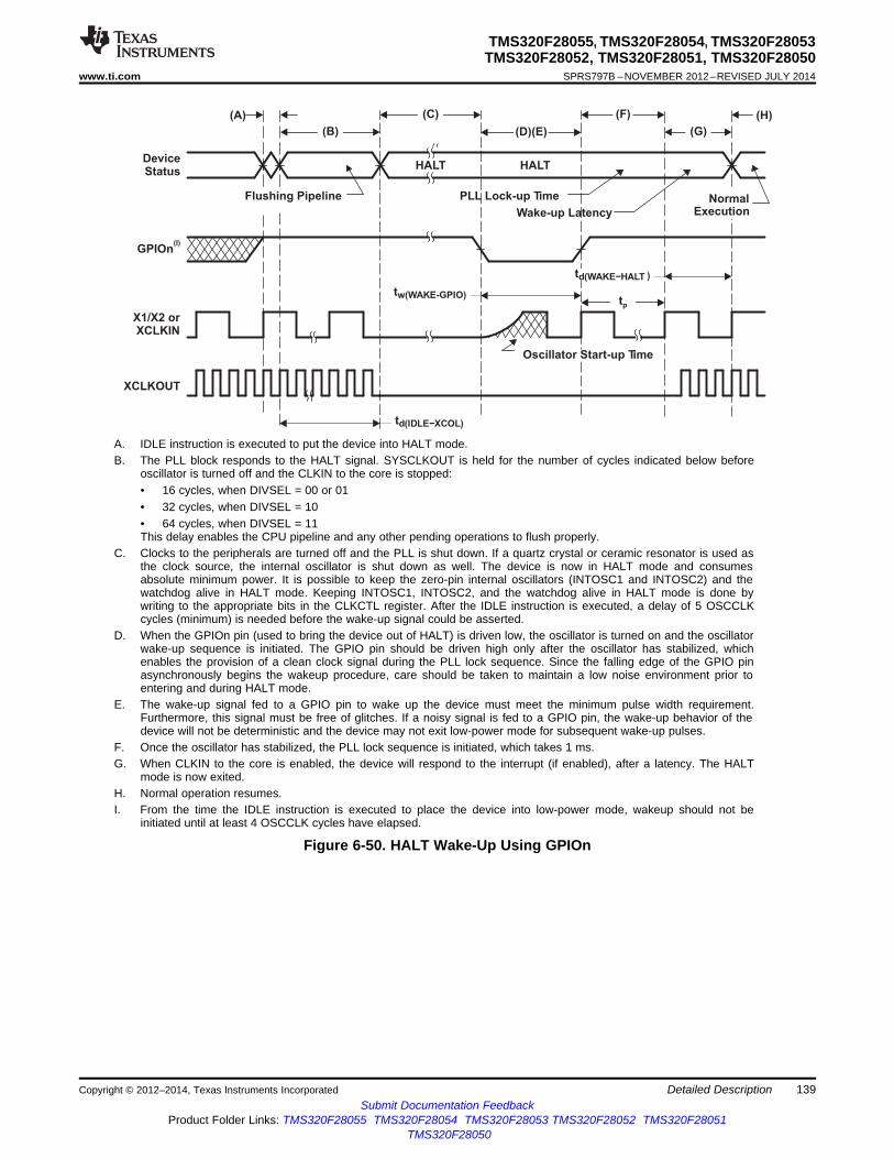
td(IDLE−XCOL)
X1/X2 orXCLKIN
XCLKOUT
HALT HALT
Wake-up Latency
Flushing Pipeline
td(WAKE−HALT
DeviceStatus
PLL Lock-up Time NormalExecution
tw(WAKE-GPIO)
GPIOn(I)
Oscillator Start-up Time
(A)
(G)
(C)
(D)(E)
(F)
(B)
(H)
)
tp
TMS320F28055, TMS320F28054, TMS320F28053TMS320F28052, TMS320F28051, TMS320F28050
www.ti.com SPRS797B –NOVEMBER 2012–REVISED JULY 2014
A. IDLE instruction is executed to put the device into HALT mode.B. The PLL block responds to the HALT signal. SYSCLKOUT is held for the number of cycles indicated below before
oscillator is turned off and the CLKIN to the core is stopped:• 16 cycles, when DIVSEL = 00 or 01• 32 cycles, when DIVSEL = 10• 64 cycles, when DIVSEL = 11This delay enables the CPU pipeline and any other pending operations to flush properly.
C. Clocks to the peripherals are turned off and the PLL is shut down. If a quartz crystal or ceramic resonator is used asthe clock source, the internal oscillator is shut down as well. The device is now in HALT mode and consumesabsolute minimum power. It is possible to keep the zero-pin internal oscillators (INTOSC1 and INTOSC2) and thewatchdog alive in HALT mode. Keeping INTOSC1, INTOSC2, and the watchdog alive in HALT mode is done bywriting to the appropriate bits in the CLKCTL register. After the IDLE instruction is executed, a delay of 5 OSCCLKcycles (minimum) is needed before the wake-up signal could be asserted.
D. When the GPIOn pin (used to bring the device out of HALT) is driven low, the oscillator is turned on and the oscillatorwake-up sequence is initiated. The GPIO pin should be driven high only after the oscillator has stabilized, whichenables the provision of a clean clock signal during the PLL lock sequence. Since the falling edge of the GPIO pinasynchronously begins the wakeup procedure, care should be taken to maintain a low noise environment prior toentering and during HALT mode.
E. The wake-up signal fed to a GPIO pin to wake up the device must meet the minimum pulse width requirement.Furthermore, this signal must be free of glitches. If a noisy signal is fed to a GPIO pin, the wake-up behavior of thedevice will not be deterministic and the device may not exit low-power mode for subsequent wake-up pulses.
F. Once the oscillator has stabilized, the PLL lock sequence is initiated, which takes 1 ms.G. When CLKIN to the core is enabled, the device will respond to the interrupt (if enabled), after a latency. The HALT
mode is now exited.H. Normal operation resumes.I. From the time the IDLE instruction is executed to place the device into low-power mode, wakeup should not be
initiated until at least 4 OSCCLK cycles have elapsed.
Figure 6-50. HALT Wake-Up Using GPIOn
Copyright © 2012–2014, Texas Instruments Incorporated Detailed Description 139Submit Documentation Feedback
Product Folder Links: TMS320F28055 TMS320F28054 TMS320F28053 TMS320F28052 TMS320F28051TMS320F28050

TMS320F28055, TMS320F28054, TMS320F28053TMS320F28052, TMS320F28051, TMS320F28050SPRS797B –NOVEMBER 2012–REVISED JULY 2014 www.ti.com
7 Device and Documentation Support
7.1 Device Support
7.1.1 Development SupportTexas Instruments (TI) offers an extensive line of development tools for the C28x generation of MCUs,including tools to evaluate the performance of the processors, generate code, develop algorithmimplementations, and fully integrate and debug software and hardware modules.
The following products support development of 2805x-based applications:
Software Development Tools• Code Composer Studio™ Integrated Development Environment (IDE)
– C/C++ Compiler– Code generation tools– Assembler/Linker– Cycle Accurate Simulator
• Application algorithms• Sample applications code
Hardware Development Tools• Development and evaluation boards• JTAG-based emulators – XDS510™ class, XDS560™ emulator, XDS100• Flash programming tools• Power supply• Documentation and cables
For a complete listing of development-support tools for the processor platform, visit the Texas Instrumentswebsite at www.ti.com. For information on pricing and availability, contact the nearest TI field sales officeor authorized distributor.
7.1.1.1 Getting Started
This section gives a brief overview of the steps to take when first developing for a C28x device. For moredetail on each of these steps, see the following:• Getting Started With TMS320C28x Digital Signal Controllers (SPRAAM0).• C2000 Getting Started Website (http://www.ti.com/c2000getstarted)• TMS320F28x MCU Development and Experimenter's Kits (http://www.ti.com/f28xkits)
140 Device and Documentation Support Copyright © 2012–2014, Texas Instruments IncorporatedSubmit Documentation Feedback
Product Folder Links: TMS320F28055 TMS320F28054 TMS320F28053 TMS320F28052 TMS320F28051TMS320F28050

TMS320F28055, TMS320F28054, TMS320F28053TMS320F28052, TMS320F28051, TMS320F28050
www.ti.com SPRS797B –NOVEMBER 2012–REVISED JULY 2014
7.1.2 Device and Development Support Tool NomenclatureTo designate the stages in the product development cycle, TI assigns prefixes to the part numbers of allTMS320™ MCU devices and support tools. Each TMS320 MCU commercial family member has one ofthree prefixes: TMX, TMP, or TMS (for example, TMS320F28055). Texas Instruments recommends two ofthree possible prefix designators for its support tools: TMDX and TMDS. These prefixes representevolutionary stages of product development from engineering prototypes (with TMX for devices and TMDXfor tools) through fully qualified production devices and tools (with TMS for devices and TMDS for tools).
Device development evolutionary flow:
TMX Experimental device that is not necessarily representative of the final device's electricalspecifications
TMP Final silicon die that conforms to the device's electrical specifications but has notcompleted quality and reliability verification
TMS Fully qualified production device
Support tool development evolutionary flow:
TMDX Development-support product that has not yet completed Texas Instruments internalqualification testing
TMDS Fully qualified development-support product
TMX and TMP devices and TMDX development-support tools are shipped against the followingdisclaimer:"Developmental product is intended for internal evaluation purposes."
TMS devices and TMDS development-support tools have been characterized fully, and the quality andreliability of the device have been demonstrated fully. TI's standard warranty applies.
Predictions show that prototype devices (TMX or TMP) have a greater failure rate than the standardproduction devices. Texas Instruments recommends that these devices not be used in any productionsystem because their expected end-use failure rate still is undefined. Only qualified production devices areto be used.
TI device nomenclature also includes a suffix with the device family name. This suffix indicates thepackage type (for example, PN) and temperature range (for example, T). Figure 7-1 provides a legend forreading the complete device name for any family member.
For device part numbers and further ordering information, see the TI website (www.ti.com) or contact yourTI sales representative.
For additional description of the device nomenclature markings on the die, see the TMS320F28055,TMS320F28054, TMS320F28053, TMS320F28052, TMS320F28051, TMS320F28050 Piccolo MCUSilicon Errata (SPRZ362).
Copyright © 2012–2014, Texas Instruments Incorporated Device and Documentation Support 141Submit Documentation Feedback
Product Folder Links: TMS320F28055 TMS320F28054 TMS320F28053 TMS320F28052 TMS320F28051TMS320F28050

PREFIX
TMS
TMX = experimental deviceTMP = prototype deviceTMS = qualified device
320
DEVICE FAMILY
320 = TMS320 MCU Family
F
TECHNOLOGY
F = Flash
28055
DEVICE
280552805428053280522805128050
PN
PACKAGE TYPE
80-Pin PN Low-Profile Quad Flatpack (LQFP)
TEMPERATURE RANGE
T
−40°C to 105°C−40°C to 125°C−40°C to 125°C(Q refers to Q100 qualificationfor automotive applications.)
TSQ
===
TMS320F28055, TMS320F28054, TMS320F28053TMS320F28052, TMS320F28051, TMS320F28050SPRS797B –NOVEMBER 2012–REVISED JULY 2014 www.ti.com
Figure 7-1. Device Nomenclature
142 Device and Documentation Support Copyright © 2012–2014, Texas Instruments IncorporatedSubmit Documentation Feedback
Product Folder Links: TMS320F28055 TMS320F28054 TMS320F28053 TMS320F28052 TMS320F28051TMS320F28050

TMS320F28055, TMS320F28054, TMS320F28053TMS320F28052, TMS320F28051, TMS320F28050
www.ti.com SPRS797B –NOVEMBER 2012–REVISED JULY 2014
7.2 Documentation SupportExtensive documentation supports all of the TMS320 MCU family generations of devices from productannouncement through applications development. The types of documentation available include: datasheets and data manuals, with design specifications; and hardware and software applications.
The following documents can be downloaded from the TI website (www.ti.com):
Data Manual and ErrataSPRS797 TMS320F28055, TMS320F28054, TMS320F28053, TMS320F28052, TMS320F28051,
TMS320F28050 Piccolo Microcontrollers Data Manual contains the pinout, signaldescriptions, as well as electrical and timing specifications for the 2805x devices.
SPRZ362 TMS320F28055, TMS320F28054, TMS320F28053, TMS320F28052, TMS320F28051,TMS320F28050 Piccolo MCU Silicon Errata describes known advisories on silicon andprovides workarounds.
InstaSPIN Technical Reference ManualsSPRUHJ1 InstaSPIN-FOC™ and InstaSPIN-MOTION™ User's Guide describes the InstaSPIN-FOC
and InstaSPIN-MOTION devices.
SPRUHW0 TMS320F28054F, TMS320F28052F InstaSPIN-FOC™ Software Technical ReferenceManual describes TMS320F28054F and TMS320F28052F InstaSPIN-FOC software.
SPRUHW1 TMS320F28054M, TMS320F28052M InstaSPIN-MOTION™ Software TechnicalReference Manual describes TMS320F28054M and TMS320F28052M InstaSPIN-MOTIONsoftware.
Technical Reference ManualSPRUHE5 TMS320x2805x Piccolo Technical Reference Manual details the integration, the
environment, the functional description, and the programming models for each peripheraland subsystem in the 2805x microcontrollers.
CPU User's GuidesSPRU430 TMS320C28x CPU and Instruction Set Reference Guide describes the central processing
unit (CPU) and the assembly language instructions of the TMS320C28x fixed-point digitalsignal processors (DSPs). This Reference Guide also describes emulation features availableon these DSPs.
Peripheral GuidesSPRU566 TMS320x28xx, 28xxx DSP Peripheral Reference Guide describes the peripheral reference
guides of the 28x digital signal processors (DSPs).
Tools GuidesSPRU513 TMS320C28x Assembly Language Tools v6.2.4 User's Guide describes the assembly
language tools (assembler and other tools used to develop assembly language code),assembler directives, macros, common object file format, and symbolic debugging directivesfor the TMS320C28x device.
SPRU514 TMS320C28x Optimizing C/C++ Compiler v6.2.4 User's Guide describes theTMS320C28x C/C++ compiler. This compiler accepts ANSI standard C/C++ source codeand produces TMS320 digital signal processor (DSP) assembly language source code forthe TMS320C28x device.
SPRU608 TMS320C28x Instruction Set Simulator Technical Overview describes the simulator,available within the Code Composer Studio for TMS320C2000 IDE, that simulates theinstruction set of the C28x core.
Copyright © 2012–2014, Texas Instruments Incorporated Device and Documentation Support 143Submit Documentation Feedback
Product Folder Links: TMS320F28055 TMS320F28054 TMS320F28053 TMS320F28052 TMS320F28051TMS320F28050

TMS320F28055, TMS320F28054, TMS320F28053TMS320F28052, TMS320F28051, TMS320F28050SPRS797B –NOVEMBER 2012–REVISED JULY 2014 www.ti.com
Application ReportsSZZA021 Semiconductor Packing Methodology describes the packing methodologies employed to
prepare semiconductor devices for shipment to end users.
7.3 Related LinksThe table below lists quick access links. Categories include technical documents, support and communityresources, tools and software, and quick access to sample or buy.
Table 7-1. Related Links
TECHNICAL TOOLS & SUPPORT &PARTS PRODUCT FOLDER SAMPLE & BUY DOCUMENTS SOFTWARE COMMUNITYTMS320F28055 Click here Click here Click here Click here Click hereTMS320F28054 Click here Click here Click here Click here Click hereTMS320F28053 Click here Click here Click here Click here Click hereTMS320F28052 Click here Click here Click here Click here Click hereTMS320F28051 Click here Click here Click here Click here Click hereTMS320F28050 Click here Click here Click here Click here Click here
7.4 Community ResourcesThe following links connect to TI community resources. Linked contents are provided "AS IS" by therespective contributors. They do not constitute TI specifications and do not necessarily reflect TI's views;see TI's Terms of Use.
TI E2E™ Online Community TI's Engineer-to-Engineer (E2E) Community. Created to fostercollaboration among engineers. At e2e.ti.com, you can ask questions, share knowledge,explore ideas and help solve problems with fellow engineers.
TI Embedded Processors Wiki Texas Instruments Embedded Processors Wiki. Established to helpdevelopers get started with Embedded Processors from Texas Instruments and to fosterinnovation and growth of general knowledge about the hardware and software surroundingthese devices.
7.5 TrademarksPiccolo, InstaSPIN-MOTION, InstaSPIN-FOC, InstaSPIN, TMS320C2000, DSP/BIOS, Code ComposerStudio, XDS510, XDS560, TMS320, E2E are trademarks of Texas Instruments.All other trademarks are the property of their respective owners.
7.6 Electrostatic Discharge CautionThis integrated circuit can be damaged by ESD. Texas Instruments recommends that all integrated circuits be handled withappropriate precautions. Failure to observe proper handling and installation procedures can cause damage.
ESD damage can range from subtle performance degradation to complete device failure. Precision integrated circuits may be moresusceptible to damage because very small parametric changes could cause the device not to meet its published specifications.
7.7 GlossarySLYZ022 — TI Glossary.
This glossary lists and explains terms, acronyms, and definitions.
144 Device and Documentation Support Copyright © 2012–2014, Texas Instruments IncorporatedSubmit Documentation Feedback
Product Folder Links: TMS320F28055 TMS320F28054 TMS320F28053 TMS320F28052 TMS320F28051TMS320F28050

TMS320F28055, TMS320F28054, TMS320F28053TMS320F28052, TMS320F28051, TMS320F28050
www.ti.com SPRS797B –NOVEMBER 2012–REVISED JULY 2014
8 Mechanical Packaging and Orderable Information
8.1 Packaging InformationThe following pages include mechanical packaging and orderable information. This information is the mostcurrent data available for the designated devices. This data is subject to change without notice andrevision of this document. For browser-based versions of this data sheet, refer to the left-hand navigation.
Copyright © 2012–2014, Texas Instruments Incorporated Mechanical Packaging and Orderable Information 145Submit Documentation Feedback
Product Folder Links: TMS320F28055 TMS320F28054 TMS320F28053 TMS320F28052 TMS320F28051TMS320F28050

PACKAGE OPTION ADDENDUM
www.ti.com 6-Dec-2016
Addendum-Page 1
PACKAGING INFORMATION
Orderable Device Status(1)
Package Type PackageDrawing
Pins PackageQty
Eco Plan(2)
Lead/Ball Finish(6)
MSL Peak Temp(3)
Op Temp (°C) Device Marking(4/5)
Samples
TMS320F28050PNQ ACTIVE LQFP PN 80 119 Green (RoHS& no Sb/Br)
CU NIPDAU Level-3-260C-168 HR -40 to 125 F28050PNQTMS320
TMS320F28050PNS ACTIVE LQFP PN 80 119 Green (RoHS& no Sb/Br)
CU NIPDAU Level-3-260C-168 HR -40 to 125 F28050PNSTMS320
TMS320F28050PNT ACTIVE LQFP PN 80 119 Green (RoHS& no Sb/Br)
CU NIPDAU Level-3-260C-168 HR -40 to 105 F28050PNTTMS320
TMS320F28051PNQ ACTIVE LQFP PN 80 119 Green (RoHS& no Sb/Br)
CU NIPDAU Level-3-260C-168 HR -40 to 125 F28051PNQTMS320
TMS320F28051PNS ACTIVE LQFP PN 80 119 Green (RoHS& no Sb/Br)
CU NIPDAU Level-3-260C-168 HR -40 to 125 F28051PNSTMS320
TMS320F28051PNT ACTIVE LQFP PN 80 119 Green (RoHS& no Sb/Br)
CU NIPDAU Level-3-260C-168 HR -40 to 105 F28051PNTTMS320
TMS320F28052FPNQ ACTIVE LQFP PN 80 119 Green (RoHS& no Sb/Br)
CU NIPDAU Level-3-260C-168 HR -40 to 125 F28052FPNQTMS320
TMS320F28052FPNT ACTIVE LQFP PN 80 119 Green (RoHS& no Sb/Br)
CU NIPDAU Level-3-260C-168 HR -40 to 105 F28052FPNTTMS320
TMS320F28052MPNQ ACTIVE LQFP PN 80 119 Green (RoHS& no Sb/Br)
CU NIPDAU Level-3-260C-168 HR -40 to 125 F28052MPNQTMS320
TMS320F28052MPNT ACTIVE LQFP PN 80 119 Green (RoHS& no Sb/Br)
CU NIPDAU Level-3-260C-168 HR -40 to 105 F28052MPNTTMS320
TMS320F28052PNQ ACTIVE LQFP PN 80 119 Green (RoHS& no Sb/Br)
CU NIPDAU Level-3-260C-168 HR -40 to 125 F28052PNQTMS320
TMS320F28052PNS ACTIVE LQFP PN 80 119 Green (RoHS& no Sb/Br)
CU NIPDAU Level-3-260C-168 HR -40 to 125 F28052PNSTMS320
TMS320F28052PNT ACTIVE LQFP PN 80 119 Green (RoHS& no Sb/Br)
CU NIPDAU Level-3-260C-168 HR -40 to 105 F28052PNTTMS320
TMS320F28053PNQ ACTIVE LQFP PN 80 119 Green (RoHS& no Sb/Br)
CU NIPDAU Level-3-260C-168 HR -40 to 125 F28053PNQTMS320
TMS320F28053PNS ACTIVE LQFP PN 80 119 Green (RoHS& no Sb/Br)
CU NIPDAU Level-3-260C-168 HR -40 to 125 F28053PNSTMS320
TMS320F28053PNT ACTIVE LQFP PN 80 119 Green (RoHS& no Sb/Br)
CU NIPDAU Level-3-260C-168 HR -40 to 105 F28053PNTTMS320
TMS320F28054FPNQ ACTIVE LQFP PN 80 119 Green (RoHS& no Sb/Br)
CU NIPDAU Level-3-260C-168 HR -40 to 125 F28054FPNQTMS320
PACKAGE OPTION ADDENDUM
www.ti.com 6-Dec-2016
Addendum-Page 2
Orderable Device Status(1)
Package Type PackageDrawing
Pins PackageQty
Eco Plan(2)
Lead/Ball Finish(6)
MSL Peak Temp(3)
Op Temp (°C) Device Marking(4/5)
Samples
TMS320F28054FPNT ACTIVE LQFP PN 80 119 Green (RoHS& no Sb/Br)
CU NIPDAU Level-3-260C-168 HR -40 to 105 F28054FPNTTMS320
TMS320F28054MPNQ ACTIVE LQFP PN 80 119 Green (RoHS& no Sb/Br)
CU NIPDAU Level-3-260C-168 HR -40 to 125 F28054MPNQTMS320
TMS320F28054MPNT ACTIVE LQFP PN 80 119 Green (RoHS& no Sb/Br)
CU NIPDAU Level-3-260C-168 HR -40 to 105 F28054MPNTTMS320
TMS320F28054PNQ ACTIVE LQFP PN 80 119 Green (RoHS& no Sb/Br)
CU NIPDAU Level-3-260C-168 HR -40 to 125 F28054PNQTMS320
TMS320F28054PNS ACTIVE LQFP PN 80 119 Green (RoHS& no Sb/Br)
CU NIPDAU Level-3-260C-168 HR -40 to 125 F28054PNSTMS320
TMS320F28054PNT ACTIVE LQFP PN 80 119 Green (RoHS& no Sb/Br)
CU NIPDAU Level-3-260C-168 HR -40 to 105 F28054PNTTMS320
TMS320F28055PNQ ACTIVE LQFP PN 80 119 Green (RoHS& no Sb/Br)
CU NIPDAU Level-3-260C-168 HR -40 to 125 F28055PNQTMS320
TMS320F28055PNS ACTIVE LQFP PN 80 119 Green (RoHS& no Sb/Br)
CU NIPDAU Level-3-260C-168 HR -40 to 125 F28055PNSTMS320
TMS320F28055PNT ACTIVE LQFP PN 80 119 Green (RoHS& no Sb/Br)
CU NIPDAU Level-3-260C-168 HR -40 to 105 F28055PNTTMS320
(1) The marketing status values are defined as follows:ACTIVE: Product device recommended for new designs.LIFEBUY: TI has announced that the device will be discontinued, and a lifetime-buy period is in effect.NRND: Not recommended for new designs. Device is in production to support existing customers, but TI does not recommend using this part in a new design.PREVIEW: Device has been announced but is not in production. Samples may or may not be available.OBSOLETE: TI has discontinued the production of the device.
(2) Eco Plan - The planned eco-friendly classification: Pb-Free (RoHS), Pb-Free (RoHS Exempt), or Green (RoHS & no Sb/Br) - please check http://www.ti.com/productcontent for the latest availabilityinformation and additional product content details.TBD: The Pb-Free/Green conversion plan has not been defined.Pb-Free (RoHS): TI's terms "Lead-Free" or "Pb-Free" mean semiconductor products that are compatible with the current RoHS requirements for all 6 substances, including the requirement thatlead not exceed 0.1% by weight in homogeneous materials. Where designed to be soldered at high temperatures, TI Pb-Free products are suitable for use in specified lead-free processes.Pb-Free (RoHS Exempt): This component has a RoHS exemption for either 1) lead-based flip-chip solder bumps used between the die and package, or 2) lead-based die adhesive used betweenthe die and leadframe. The component is otherwise considered Pb-Free (RoHS compatible) as defined above.Green (RoHS & no Sb/Br): TI defines "Green" to mean Pb-Free (RoHS compatible), and free of Bromine (Br) and Antimony (Sb) based flame retardants (Br or Sb do not exceed 0.1% by weightin homogeneous material)
(3) MSL, Peak Temp. - The Moisture Sensitivity Level rating according to the JEDEC industry standard classifications, and peak solder temperature.

PACKAGE OPTION ADDENDUM
www.ti.com 6-Dec-2016
Addendum-Page 3
(4) There may be additional marking, which relates to the logo, the lot trace code information, or the environmental category on the device.
(5) Multiple Device Markings will be inside parentheses. Only one Device Marking contained in parentheses and separated by a "~" will appear on a device. If a line is indented then it is a continuationof the previous line and the two combined represent the entire Device Marking for that device.
(6) Lead/Ball Finish - Orderable Devices may have multiple material finish options. Finish options are separated by a vertical ruled line. Lead/Ball Finish values may wrap to two lines if the finishvalue exceeds the maximum column width.
Important Information and Disclaimer:The information provided on this page represents TI's knowledge and belief as of the date that it is provided. TI bases its knowledge and belief on informationprovided by third parties, and makes no representation or warranty as to the accuracy of such information. Efforts are underway to better integrate information from third parties. TI has taken andcontinues to take reasonable steps to provide representative and accurate information but may not have conducted destructive testing or chemical analysis on incoming materials and chemicals.TI and TI suppliers consider certain information to be proprietary, and thus CAS numbers and other limited information may not be available for release.
In no event shall TI's liability arising out of such information exceed the total purchase price of the TI part(s) at issue in this document sold by TI to Customer on an annual basis.

MECHANICAL DATA
MTQF010A – JANUARY 1995 – REVISED DECEMBER 1996
1POST OFFICE BOX 655303 • DALLAS, TEXAS 75265
PN (S-PQFP-G80) PLASTIC QUAD FLATPACK
4040135 /B 11/96
0,170,27
0,13 NOM
40
21
0,25
0,450,75
0,05 MIN
Seating Plane
Gage Plane
4160
61
80
20
SQ
SQ
1
13,8014,20
12,20
9,50 TYP
11,80
1,451,35
1,60 MAX 0,08
0,50 M0,08
0°–7°
NOTES: A. All linear dimensions are in millimeters.B. This drawing is subject to change without notice.C. Falls within JEDEC MS-026

IMPORTANT NOTICE
Texas Instruments Incorporated and its subsidiaries (TI) reserve the right to make corrections, enhancements, improvements and otherchanges to its semiconductor products and services per JESD46, latest issue, and to discontinue any product or service per JESD48, latestissue. Buyers should obtain the latest relevant information before placing orders and should verify that such information is current andcomplete. All semiconductor products (also referred to herein as “components”) are sold subject to TI’s terms and conditions of salesupplied at the time of order acknowledgment.TI warrants performance of its components to the specifications applicable at the time of sale, in accordance with the warranty in TI’s termsand conditions of sale of semiconductor products. Testing and other quality control techniques are used to the extent TI deems necessaryto support this warranty. Except where mandated by applicable law, testing of all parameters of each component is not necessarilyperformed.TI assumes no liability for applications assistance or the design of Buyers’ products. Buyers are responsible for their products andapplications using TI components. To minimize the risks associated with Buyers’ products and applications, Buyers should provideadequate design and operating safeguards.TI does not warrant or represent that any license, either express or implied, is granted under any patent right, copyright, mask work right, orother intellectual property right relating to any combination, machine, or process in which TI components or services are used. Informationpublished by TI regarding third-party products or services does not constitute a license to use such products or services or a warranty orendorsement thereof. Use of such information may require a license from a third party under the patents or other intellectual property of thethird party, or a license from TI under the patents or other intellectual property of TI.Reproduction of significant portions of TI information in TI data books or data sheets is permissible only if reproduction is without alterationand is accompanied by all associated warranties, conditions, limitations, and notices. TI is not responsible or liable for such altereddocumentation. Information of third parties may be subject to additional restrictions.Resale of TI components or services with statements different from or beyond the parameters stated by TI for that component or servicevoids all express and any implied warranties for the associated TI component or service and is an unfair and deceptive business practice.TI is not responsible or liable for any such statements.Buyer acknowledges and agrees that it is solely responsible for compliance with all legal, regulatory and safety-related requirementsconcerning its products, and any use of TI components in its applications, notwithstanding any applications-related information or supportthat may be provided by TI. Buyer represents and agrees that it has all the necessary expertise to create and implement safeguards whichanticipate dangerous consequences of failures, monitor failures and their consequences, lessen the likelihood of failures that might causeharm and take appropriate remedial actions. Buyer will fully indemnify TI and its representatives against any damages arising out of the useof any TI components in safety-critical applications.In some cases, TI components may be promoted specifically to facilitate safety-related applications. With such components, TI’s goal is tohelp enable customers to design and create their own end-product solutions that meet applicable functional safety standards andrequirements. Nonetheless, such components are subject to these terms.No TI components are authorized for use in FDA Class III (or similar life-critical medical equipment) unless authorized officers of the partieshave executed a special agreement specifically governing such use.Only those TI components which TI has specifically designated as military grade or “enhanced plastic” are designed and intended for use inmilitary/aerospace applications or environments. Buyer acknowledges and agrees that any military or aerospace use of TI componentswhich have not been so designated is solely at the Buyer's risk, and that Buyer is solely responsible for compliance with all legal andregulatory requirements in connection with such use.TI has specifically designated certain components as meeting ISO/TS16949 requirements, mainly for automotive use. In any case of use ofnon-designated products, TI will not be responsible for any failure to meet ISO/TS16949.
Products ApplicationsAudio www.ti.com/audio Automotive and Transportation www.ti.com/automotiveAmplifiers amplifier.ti.com Communications and Telecom www.ti.com/communicationsData Converters dataconverter.ti.com Computers and Peripherals www.ti.com/computersDLP® Products www.dlp.com Consumer Electronics www.ti.com/consumer-appsDSP dsp.ti.com Energy and Lighting www.ti.com/energyClocks and Timers www.ti.com/clocks Industrial www.ti.com/industrialInterface interface.ti.com Medical www.ti.com/medicalLogic logic.ti.com Security www.ti.com/securityPower Mgmt power.ti.com Space, Avionics and Defense www.ti.com/space-avionics-defenseMicrocontrollers microcontroller.ti.com Video and Imaging www.ti.com/videoRFID www.ti-rfid.comOMAP Applications Processors www.ti.com/omap TI E2E Community e2e.ti.comWireless Connectivity www.ti.com/wirelessconnectivity
Mailing Address: Texas Instruments, Post Office Box 655303, Dallas, Texas 75265Copyright © 2016, Texas Instruments Incorporated