Embed Size (px)
Citation preview

Document Number: MC33689Rev. 8.0, 9/2012
Freescale Semiconductor Technical Data
Fa©
System Basis Chip with LIN Transceiver
The 33689 is a serial peripheral interface (SPI) controlled system basis chip (SBC) that combines many frequently used functions in an MCU-based system plus a local interconnect network (LIN) transceiver. Applications include power window, mirror, and seat controls. The 33689 has a 5.0 V, 50 mA low dropout regulator with full protection and reporting features. The device provides full SPI-readable diagnostics and a selectable timing watchdog for detecting errant operation.
The LIN transceiver waveshaping circuitry can be disabled for higher data rates. One 50 mA and two 150 mA high side switches with output protection are available to drive inductive or resistive loads. The 150 mA switches can be pulse-width modulated (PWM).
Two high voltage inputs are available for contact monitoring or as external wake-up inputs. A current sense operational amplifier is available for load current monitoring.
The 33689 has three operational modes: • Normal (all functions available)• Sleep (VDD OFF, wake-up via LIN bus or wake-up inputs)• Stop (VDD ON, wake-up via MCU, LIN bus, or wake-up inputs)
Features• Full-duplex SPI Interface at frequencies up to 4.0 MHz• LIN transceiver capable to 100 kbps with waveshaping capability• 5.0 V low dropout regulator with full fault detection and protection• One 50 mA and two 150 mA protected high side switches • Current sense operational amplifier• Compatible with LIN 2.0 specification package
Figure 1. 33689 Simplified Application Diagram
SYSTEM BASIS CHIP WITH LIN
33689D
ORDERING INFORMATION
Device (Add R2 Suffix for Tape
and Reel)
Temperature Range (TA) Package
MC33689DPEW -40 °C to 125 °C 32 SOICW
EW SUFFIX (PB-FREE)98ARH99137A32-PIN SOICW
VPWR
SPIMOSISCK
MISO
5.0 V
MCU
33689
BUS
VS1
VS2
VDD
HS3
L1L2
HS1
HS2
E+
LIN
INTRST
MOSISCLK
MISO
TXDRXD
OUT
GNDIN
CS CS
WDC
E-
TGND
AGND
VDD
VCC
reescale Semiconductor, Inc. reserves the right to change the detail specifications, s may be required, to permit improvements in the design of its products. Freescale Semiconductor, Inc., 2006-2012. All rights reserved.

INTERNAL BLOCK DIAGRAM
INTERNAL BLOCK DIAGRAM
Figure 2. 33689 Simplified Internal Block Diagram
LIN
L1
L2
VDD
HS2
HS3
E+
E-
RXD
TXD
OUT
MOSI
MISO
SCLK
SPI
and
Mode
Control
VCC
5.0 V/50 mA
IN
Voltage
Regulator
LIN Physical Interface
Window
Watchdog
Reset
Control
Pre-Driver
GND AGNDTGND
VS1
Current
Sense
Op Amp
CS
INT
WDC
RST
VS1
HS1
VS2
Analog Integrated Circuit Device Data 2 Freescale Semiconductor
33689

PIN CONNECTIONS
PIN CONNECTIONS
Figure 3. 33689 32-SOICW Pin Connections
Table 1. 33689 32-SOICW Pin Definitions
A functional description of each pin can be found in the Functional Pin Description section beginning on page 19.
Pin Pin Name Formal Name Pin Function Definition
1, 3, 14 NC No Connect N/A No internal connection to these pins.
2, 4 L1, L2 Level Inputs 1 and 2 Input Inputs from external switches or from logic circuitry.
5 – 7 HS3 – HS1 High-Side Driver Outputs 3 through 1
Output High-side (HS) drive power outputs. SPI-controlled for driving system loads.
8, 9, 24, 25 TGND Thermal Ground N/A Thermal ground pins for the device.
10 VS2 Voltage Supply 2 Input Supply pin for the high-side switches HS1, HS2, and HS3.
11 LIN LIN Bus Input / Output Bidirectional pin that represents the single-wire bus transmitter and receiver.
12 GND Ground N/A Electrical ground pin for the device.
13 VS1 Voltage Supply 1 Input Supply pin for the 5.0 V regulator, the LIN physical interface, and the internal logic.
15 VDD 5.0 V Regulator Output
Output Output of the 5.0 V regulator.
16 AGND Analog Ground N/A Analog ground pin for voltage regulator and current sense operational amplifier.
17 VCC Power Supply In Input 5.0 V supply for the internal current sense operational amplifier.
18 OUT Amplifier Output Output Output of the internal current sense operational amplifier.
19 E- Amplifier Inverted Input
Input Inverted input of the internal current sense operational amplifier.
20 E+ Amplifier Non-Inverted Input
Input Non-inverted input of the internal current sense operational amplifier.
21 WDC Watchdog Configuration(Active Low)
Reference Configuration pin for the watchdog timer.
TXD1
MISOMOSISCLKTGNDTGNDINRSTWDCE+
OUTVCC
E-
CS
RXDINT
NC
HS3HS2HS1
TGNDTGND
VS2LIN
GNDVS1
VDDAGND
NC
L2
L1NC
8910111213141516
34567
232
252423222120191817
3029282726
31
Analog Integrated Circuit Device Data Freescale Semiconductor 3
33689

PIN CONNECTIONS
22 RST Reset Output (Active LOW)
Output 5.0 V regulator and watchdog reset output pin.
23 IN PWM Input Control Input External input PWM control pin for high-side switches HS1 and HS2.
26 SCLK Serial Data Clock Input Clock input for the SPI of the 33689.
27 MOSI Master Out Slave In Input SPI data received by the 33689.
28 MISO Master In Slave Out Output SPI data sent to the MCU by the 33689. When CS is HIGH, pin is in the high-impedance state.
29 CS Chip Select (Active LOW)
Input SPI control chip select input pin.
30 INT Interrupt Output(Active LOW)
Output This output pin reports faults to the MCU when an enabled interrupt condition occurs.
31 RXD Receiver Output Output Receiver output of the LIN interface and reports the state of the bus voltage.
32 TXD Transmitter Input Input Transmitter input of the LIN interface and controls the state of the bus output.
Table 1. 33689 32-SOICW Pin Definitions (continued)A functional description of each pin can be found in the Functional Pin Description section beginning on page 19.
Pin Pin Name Formal Name Pin Function Definition
Analog Integrated Circuit Device Data 4 Freescale Semiconductor
33689

ELECTRICAL CHARACTERISTICSMAXIMUM RATINGS
ELECTRICAL CHARACTERISTICS
MAXIMUM RATINGS
Table 2. Maximum Ratings All voltages are with respect to ground unless otherwise noted. Exceeding these ratings may cause a malfunction or
permanent damage to the device.
Ratings Symbol Value Unit
ELECTRICAL RATINGS
VPWR Supply Voltage at VS1 and VS2
ContinuousTransient (Load Dump)
VSUPDC
VSUPTR
- 0.3 to 2740
V
Supply Voltage at VDD and VCC VDD - 0.3 to 5.5 V
Output Current at VDD IDD Internally Limited A
Logic Input Voltage at MOSI, SCLK, CS, IN, and TXD VINLOG - 0.3 to VDD + 0.3 V
Logic Output Voltage at MISO, INT, RST, and RXD VOUTLOG - 0.3 to VDD + 0.3 V
Input Voltage at E+ and E- VE+ / VE- - 0.3 to 7.0 V
Input Current at E+ and E- IE+ / IE- ± 20 mA
Output Voltage at OUT VOUT - 0.3 to VCC + 0.33 V
Output Current at OUT IOUT ± 20 mA
Input Voltage at L1 and L2 DC Input with a 33 kΩ Resistor Transient Input with External Component (per ISO7637 Specification) (See Figure 4, page 6)
VLXDC
VLXTR
-18 to 40
±100
V
Input / Output Voltage at LINDC VoltageTransient Input Voltage with specified External Component (per ISO7637 Specification) (See Figure 4, page 6)
VBUSDC
VBUSTR
-18 to 40
-150 to 100
V
DC Output Voltage at HS1 and HS2 Positive Negative
VHS+
VHS-
VVS2 + 0.3
Internally Clamped
V
DC Output Voltage at HS3 VHS3 - 0.3 to VVS2 + 0.3 V
ESD Voltage, Human Body Model (1) GND Configured as Ground. TGND and AGND Configured as I/O Pins
LIN, L1, and L2 All Other Pins
VESD1
± 4000± 2000
V
ESD Voltage, Charge Device Model (1) Corner Pins (Pins 1, 16, 17, and 32)All other Pins (Pins 2 – 15 and 18 – 31)
VESD2± 750± 500
V
Notes1. ESD1 testing is performed in accordance with the Human Body Model (CZAP = 100 pF, RZAP = 1500 Ω), ESD2 testing is performed in
accordance with the Charge Device Model, Robotic (CZAP = 4.0 pF).
Analog Integrated Circuit Device Data Freescale Semiconductor 5
33689

ELECTRICAL CHARACTERISTICSMAXIMUM RATINGS
THERMAL RATINGS
Operating TemperatureAmbientJunction
TA
TJ
- 40 to 125- 40 to 150
°C
Storage Temperature TSTG - 55 to 165 °C
Thermal Resistance, Junction-to-Ambient RθJA 80 °C/ W
Peak Package Reflow Temperature During Solder Mounting (2) TSOLDER 240 °C
Notes2. Pin soldering temperature is for 10 seconds maximum duration. Not designed for immersion soldering. Exceeding these limits may
cause permanent damage to the device.
Figure 4. ISO 7637 Test Setup for LIN, L1, and L2 Pins
Table 2. Maximum Ratings(continued)All voltages are with respect to ground unless otherwise noted. Exceeding these ratings may cause a malfunction or
permanent damage to the device.
Ratings Symbol Value Unit
LIN, L1, L2
Transient Pulse
GND
Generator1.0 nF
(Note)10 kΩ
Note Waveform per ISO 7637-1. Test Pulses 1, 2, 3a, and 3b.
GND
33689D
TGND AGND
Analog Integrated Circuit Device Data 6 Freescale Semiconductor
33689

ELECTRICAL CHARACTERISTICSSTATIC ELECTRICAL CHARACTERISTICS
STATIC ELECTRICAL CHARACTERISTICS
Table 3. Static Electrical Characteristics Characteristics noted under conditions 5.5 V ≤ VSUP ≤ 18 V, - 40°C ≤ TA ≤ 125°C, GND = 0.0 V unless otherwise noted.
Typical values noted reflect the approximate parameter means at TA = 25°C under nominal conditions unless otherwise noted.
Characteristic Symbol Min Typ Max Unit
VS1 AND VS2 INPUT PINS (DEVICE POWER SUPPLY)
Supply Input VoltageNominal DCLoad Dump
Jump Start (3)
VSUP
VSUPLD
VSUPJS
5.5——
———
184027
V
Supply Input Current (4)
Normal Mode, IOUT at VDD = 10 mA, LIN Recessive State
Sleep Mode, VDD OFF, VSUP ≤ 13.5 V
Stop Mode, VDD ON with IOUT < 100 μA, VSUP ≤ 13.5 V
ISUP(NORM)
ISLEEP
ISTOP
—
—
—
5.0
35
60
8.0
45
75
mA
μA
μA
Input Threshold Voltage (Normal Mode, Interrupt Generated)Fall Early Warning, Bit VSUV SetOvervoltage Warning, Bit VSOV Set
VSUVEW
VSOVW
5.718
6.119.75
6.620.5
V
Hysteresis (5)
VSUV FlagVSOV Flag
VHYS——
1.0220
——
VmV
VDD OUTPUT PIN (EXTERNAL 5.0 V OUTPUT FOR MCU USE) (6)
Output VoltageIDD from 2.0 mA to 50 mA, 5.5 V < VSUP < 27 V
VDDOUT4.75 5.0 5.25
V
Dropout Voltage (7)
IDD = 50 mA
VDDDROP— 0.1 0.2
V
Output Current Limitation (8) IDD 50 120 200 mA
Overtemperature Pre-warning (Junction) Normal Mode, Interrupt Generated, Bit VDDT Set
TPRE120 135 160
°C
Thermal Shutdown (Junction) Normal Mode
TSD165 170 —
°C
Notes3. Device is fully functional. All features are operating. An overtemperature fault may occur.4. Total current (IVS1 + IVS2) at VS1 and VS2 pins is measured at the ground pins.5. Parameter guaranteed by design; however, it is not production tested.6. Specification with external capacitor 2.0 μF < C < 10 μF and 200 mΩ ≤ ESR ≤ 10 Ω. Normal mode. Low ESR electrolytic capacitor values
up to 47 μF can be used.7. Measured when the voltage has dropped 100 mV below its nominal value.8. Internally limited. Total 5.0 V regulator current. A 5.0 mA current for the Current Sense Operational Amplifier operation is included.
Digital outputs are supplied from VDD.
Analog Integrated Circuit Device Data Freescale Semiconductor 7
33689

ELECTRICAL CHARACTERISTICSSTATIC ELECTRICAL CHARACTERISTICS
VDD OUTPUT PIN (5.0 V OUTPUT FOR MCU USE) (CONTINUED) (9)
Temperature Threshold Difference Normal Mode (TSD - TPRE)
TDIFF20 30 40
°C
VSUP Range for Reset Active
0.5 V < VDD < VDD (V RSTTH)
VSUPR4.0 — —
V
Line Regulation5.5 V < VSUP < 27 V, IDD = 10 mA
VLR1— 20 150
mV
Load Regulation1.0 mA < IDD < 50 mA
VLD1— 10 150
mV
VDD OUTPUT PIN IN STOP MODE
Output Voltage (10) IDD ≤ 2.0 mA
VDDS4.75 5.0 5.25
V
Output Current Capability (11) IDDS 4.0 8.0 14 mA
Line Regulation5.5 V < VSUP < 27 V, IDD = 2.0 mA
VLRS— 10 100
mV
Load Regulation1.0 mA < IDD < 5.0 mA
VLDS— 40 150
mV
RST OUTPUT PIN IN NORMAL AND STOP MODES
Reset Threshold Voltage V RSTTH 4.5 4.7 VDD - 0.2 V
Low-Level Output VoltageIO = 1.5 mA, 4.5 V < VSUP < 27 V
VOL0.0 — 0.9
V
High-Level Output Current 0.0 V < VOUT < 0.7 VDD
IOH— - 275 —
μA
Reset Pulldown CurrentInternally Limited, VDD < 4.0 V, VRST = 4.6 V
IPDRST1.5 — 8.0
mA
IN INPUT PIN
Low-Level Input Voltage VIL - 0.3 — 0.3 VDD V
High-Level Input Voltage VIH 0.7 VDD — VDD + 0.3 V
Input Current 0.0 V < VIN < VDD
IIN-10 — 10
μA
Notes9. Specification with external capacitor 2.0 μF < C < 10 μF and 200 mΩ ≤ ESR ≤ 10 Ω. Normal mode. Low ESR electrolytic capacitor values
up to 47 μF can be used.10. When switching from Normal mode to Stop mode or from Stop mode to Normal mode, the voltage can vary within the output voltage
specification.11. When IDD is above IDDS, the 33689 enters the Reset mode.
Table 3. Static Electrical Characteristics (continued)Characteristics noted under conditions 5.5 V ≤ VSUP ≤ 18 V, - 40°C ≤ TA ≤ 125°C, GND = 0.0 V unless otherwise noted.
Typical values noted reflect the approximate parameter means at TA = 25°C under nominal conditions unless otherwise noted.
Characteristic Symbol Min Typ Max Unit
Analog Integrated Circuit Device Data 8 Freescale Semiconductor
33689

ELECTRICAL CHARACTERISTICSSTATIC ELECTRICAL CHARACTERISTICS
MISO SPI OUTPUT PIN
Low-Level Output VoltageI OUT = 1.5 mA
VOL0.0 — 1.0
V
High-Level Output Voltage I OUT = 250 μA
VOHVDD - 0.9 — VDD
V
Tri-Stated MISO Output Leakage Current0.0 V < VMISO < VDD
IHZ- 2.0 — 2.0
μA
MOSI, SCLK, CS SPI INPUT PINS
Low-Level Input Voltage VIL - 0.3 — 0.3 VDD V
High-Level Input Voltage VIH 0.7 VDD — VDD + 0.3 V
Pullup Input Current on CS
VCS = 4.0 V
IPUCS-100 — - 20
μA
MOSI, SCLK Input Current 0.0 V < VIN < VDD
IIN-10 — 10
μA
INT OUTPUT PIN
Low-Level Output VoltageIO = 1.5 mA
VOL0.0 — 0.9
V
High-Level Output VoltageIO = - 250 μA
VOHVDD - 0.9 — VDD
V
WDC PIN
External Resistor Range R EXT 10 — 100 kΩ
HS1 AND HS2 HIGH-SIDE OUTPUT PINS
Output Clamp VoltageI OUT = -100 mA
VCL- 6.0 — —
V
Output Drain-to-Source ON Resistance TA = 25°C, I OUT -150 mA
TA = 125°C, I OUT -150 mA
TA = 125°C, I OUT -120 mA
RDS(ON)———
2.0—3.0
2.54.54.0
Ω
Output Current Limitation ILIM 300 430 600 mA
Overtemperature Shutdown (12) TOTSD 155 — 190 °C
Output Leakage Current ILEAK — — 10 μA
Notes12. When overtemperature occurs, switch is turned off and latched off. Flag is set in SPI Register. Refer to description on page 26.
Table 3. Static Electrical Characteristics (continued)Characteristics noted under conditions 5.5 V ≤ VSUP ≤ 18 V, - 40°C ≤ TA ≤ 125°C, GND = 0.0 V unless otherwise noted.
Typical values noted reflect the approximate parameter means at TA = 25°C under nominal conditions unless otherwise noted.
Characteristic Symbol Min Typ Max Unit
Analog Integrated Circuit Device Data Freescale Semiconductor 9
33689

ELECTRICAL CHARACTERISTICSSTATIC ELECTRICAL CHARACTERISTICS
HS3 HIGH-SIDE OUTPUT PIN
Output Drain-to-Source ON ResistanceTA = 25°C, I OUT - 50 mA
TA = 125°C, I OUT - 50 mA
TA = 125°C, I OUT - 30 mA
RDS(ON)———
5.5—10
7.01014
Ω
Output Current Limitation ILIM 60 100 200 mA
Overtemperature Shutdown (13) TOTSD 155 — 190 °C
Output Leakage Current ILEAK — — 10 μA
OUT, E+, AND E- PINS AT CURRENT SENSE OPERATIONAL AMPLIFIER
Input Voltage – Rail-to-Rail at E+ and E- VIMC - 0.1 — VCC + 0.1 V
Output Voltage Range at OUTWith ± 1.0 mA Output Load Current With ± 5.0 mA Output Load Current
VOUT0.10.3
——
VCC - 0.1VCC - 0.3
V
Input Bias Current I B — — 250 nA
Input Offset Voltage V IO -15 — 15 mV
Input Offset Current I O -100 — 100 nA
L1 AND L2 INPUT PINS
Low-Voltage Detection Input Threshold Voltage 5.5 V < VSUP < 6.0 V
6.0 V < VSUP < 18 V
18 V < VSUP < 27 V
VTHL2.02.52.7
2.53.03.2
3.03.53.7
V
High-Voltage Detection Input Threshold Voltage 5.5 V < VSUP < 6.0 V
6.0 V < VSUP < 18 V
18 V < VSUP < 27 V
VTHH2.73.03.5
3.34.04.2
3.84.54.7
V
Input Hysteresis5.5 V < VSUP < 27 V
VHYS0.5 — 1.3
V
Input Current- 0.2 V < VIN < 40 V
IIN-10 — 10
μA
Notes13. When overtemperature occurs, switch is turned off and latched off. Flag is set in SPI Register. Refer to description on page 26.
Table 3. Static Electrical Characteristics (continued)Characteristics noted under conditions 5.5 V ≤ VSUP ≤ 18 V, - 40°C ≤ TA ≤ 125°C, GND = 0.0 V unless otherwise noted.
Typical values noted reflect the approximate parameter means at TA = 25°C under nominal conditions unless otherwise noted.
Characteristic Symbol Min Typ Max Unit
Analog Integrated Circuit Device Data 10 Freescale Semiconductor
33689

ELECTRICAL CHARACTERISTICSSTATIC ELECTRICAL CHARACTERISTICS
RXD OUTPUT PIN (LIN PHYSICAL LAYER)
Low-Level Output Voltage I OUT ≤ 1.5 mA
VOL0.0 — 0.9
V
High-Level Output VoltageI OUT ≤ 250 μA
VOH3.75 — 5.25
V
TXD INPUT PIN (LIN PHYSICAL LAYER)
Low-Level Input Voltage VIL — — 1.5 V
High-Level Input Voltage VIH 3.5 — — V
Input Hysteresis VINHYS 50 145 300 mV
Pullup Current Source1.0 V < VTXD < 3.5 V
IPUTXD-100 — - 20
μA
LIN PHYSICAL LAYER, TRANSCEIVER
Transceiver Output VoltageDominant State, TXD LOW, External Bus Pullup 500 ΩRecessive State, TXD HIGH, I OUT = 1.0 μA
VLINDOM
VLINREC
—VSUP -1.0
——
1.4—
V
Pullup Resistor to VSUPIn Normal Mode and in Sleep and Stop Modes When Not Disabled by SPI
RPU
20 30 47
kΩ
Pullup Current Source In Sleep and Stop Modes When Pullup Disabled by SPI
IPULIN— 1.3 —
μA
Output Current Shutdown Threshold IOUTSD 50 75 150 mA
Leakage Output Current to GND VS1 and VS2 Disconnected, VLIN = 18 V
Recessive State, 8.0 V < VSUP < 18 V, 8.0 V < VLIN < 18 V
GND Disconnected, VGND = VSUP , VLIN = -18 V
IBUSLEAK—0.0-1.0
1.03.0—
10201.0
μAμAmA
LIN PHYSICAL LAYER, RECEIVER
Receiver Input Threshold VoltageDominant State, TXD HIGH, RXD LOWRecessive State, TXD HIGH, RXD HIGHCenter (VBUSDOM - VBUSREC) / 2
Hysteresis (VBUSDOM - VBUSREC)
VBUSDOMVBUSRECVBUSCNTVBUSHYS
0.00.6
0.475—
——0.5—
0.41.0
0.5250.175
VSUP
Bus Wake-Up Threshold VBUSWU — 0.5 — VSUP
Table 3. Static Electrical Characteristics (continued)Characteristics noted under conditions 5.5 V ≤ VSUP ≤ 18 V, - 40°C ≤ TA ≤ 125°C, GND = 0.0 V unless otherwise noted.
Typical values noted reflect the approximate parameter means at TA = 25°C under nominal conditions unless otherwise noted.
Characteristic Symbol Min Typ Max Unit
Analog Integrated Circuit Device Data Freescale Semiconductor 11
33689
ELECTRICAL CHARACTERISTICSDYNAMIC ELECTRICAL CHARACTERISTICS
33689
DYNAMIC ELECTRICAL CHARACTERISTICS
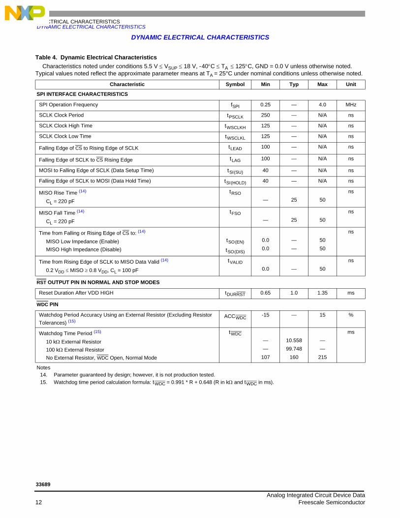
Table 4. Dynamic Electrical Characteristics
Characteristics noted under conditions 5.5 V ≤ VSUP ≤ 18 V, - 40°C ≤ TA ≤ 125°C, GND = 0.0 V unless otherwise noted. Typical values noted reflect the approximate parameter means at TA = 25°C under nominal conditions unless otherwise noted.
Characteristic Symbol Min Typ Max Unit
SPI INTERFACE CHARACTERISTICS
SPI Operation Frequency fSPI 0.25 — 4.0 MHz
SCLK Clock Period t PSCLK 250 — N/A ns
SCLK Clock High Time t WSCLKH 125 — N/A ns
SCLK Clock Low Time t WSCLKL 125 — N/A ns
Falling Edge of CS to Rising Edge of SCLK t LEAD 100 — N/A ns
Falling Edge of SCLK to CS Rising Edge t LAG 100 — N/A ns
MOSI to Falling Edge of SCLK (Data Setup Time) t SI (SU) 40 — N/A ns
Falling Edge of SCLK to MOSI (Data Hold Time) t SI (HOLD) 40 — N/A ns
MISO Rise Time (14)
CL = 220 pF
t RSO— 25 50
ns
MISO Fall Time (14)
CL = 220 pF
t FSO— 25 50
ns
Time from Falling or Rising Edge of CS to: (14) MISO Low Impedance (Enable)MISO High Impedance (Disable)
t SO (EN)
t SO (DIS)
0.00.0
——
5050
ns
Time from Rising Edge of SCLK to MISO Data Valid (14)
0.2 VDD ≤ MISO ≥ 0.8 VDD, CL = 100 pF
t VALID0.0 — 50
ns
RST OUTPUT PIN IN NORMAL AND STOP MODES
Reset Duration After VDD HIGH t DURRST 0.65 1.0 1.35 ms
WDC PIN
Watchdog Period Accuracy Using an External Resistor (Excluding Resistor Tolerances) (15)
ACC WDC -15 — 15 %
Watchdog Time Period (15)
10 kΩ External Resistor 100 kΩ External Resistor No External Resistor, WDC Open, Normal Mode
t WDC——
107
10.55899.748
160
——
215
ms
Notes14. Parameter guaranteed by design; however, it is not production tested.15. Watchdog time period calculation formula: t WDC = 0.991 * R + 0.648 (R in kΩ and t WDC in ms).
Analog Integrated Circuit Device Data 12 Freescale Semiconductor

ELECTRICAL CHARACTERISTICSDYNAMIC ELECTRICAL CHARACTERISTICS
33689
CURRENT SENSE OPERATIONAL AMPLIFIER
Supply Voltage Rejection Ratio (16) SVR 60 — — dB
Common Mode Rejection Ratio (16) CMR 70 — — dB
Gain Bandwidth (16) GBP 1.0 — — MHz
Output Slew Rate SR 0.5 — — V/μs
Phase Margin PHMO 40 — — deg.
Open Loop Gain (16) OLG — 85 — dB
L1 AND L2 INPUT PINS
Wake-Up Filter Time (16) t WUF 8.0 20 38 μs
STATE MACHINE TIMING
Delay Between CS LOW-to-HIGH Transition (at End of SPI Stop Command) and Stop Mode Activation (16)
Minimum Watchdog PeriodNo Watchdog SelectedMaximum Watchdog Period
t STOP
1.4
6.0
12
—
—
—
5.0
30
50
μs
Interrupt Low-Level Duration t INT 7.0 10 13 μs
Internal Oscillator Frequency Accuracy (All Modes, for Information Only) fOSC - 35 — 35 %
Normal Request Mode Time-Out (Normal Request Mode) t NRTOUT 97 150 205 ms
Delay Between SPI Command and HS1 or HS2 Turn On (17), (18)
Normal Mode, VSUP > 9.0 V, VHS ≥ 0.2 VVS2
t SHSON
— — 20
μs
Delay Between SPI Command and HS1 or HS2 Turn Off (17), (18) Normal Mode, VSUP > 9.0 V, VHS ≤ 0.8 VVS2
t SHSOFF
— — 20
μs
Delay Between SPI Command and HS3 Turn On (17), (19)
Normal Mode, VSUP > 9.0 V, VHS ≥ 0.2 VVS2
tSHSON
— — 20
μs
Delay Between SPI Command and HS3 Turn Off (17), (19)
Normal Mode, VSUP > 9.0 V, VHS ≤ 0.8 VVS2
tSHSOFF
— — 20
μs
Delay Between Normal Request and Normal Mode After a Watchdog Trigger Command (Normal Request Mode) (16)
t SNR2N 7.0 15 30 μs
Delay Between CS Wake-Up (CS LOW to HIGH) in Stop Mode and:Normal Request Mode, VDD ON and RST HIGHFirst Accepted SPI Command
t WUCS
t WUSPI
1590
40—
80N/A
μs
Delay Between Interrupt Pulse in Stop Mode After Wake-Up and First Accepted SPI Command
t S1STSPI 30 — N/A μs
Minimum Time Between Rising and Falling Edge on the CS t 2CS 15 — — μs
Notes16. Parameter guaranteed by design; however, it is not production tested.17. When IN input is set to HIGH, delay starts at falling edge of clock cycle #8 of the SPI command and start of device activation/deactivation.
30 mA load on high-side switches. Excluding rise or fall time due to external load.18. When IN is used to control the high-side switches, delays are measured between IN and HS1 or HS2 ON / OFF. 30 mA load on high-side
switches, excluding rise or fall time due to external load.19. Delay between turn on or turn off command and HS ON or HS OFF, excluding rise or fall time due to external load.
Table 4. Dynamic Electrical Characteristics (continued)Characteristics noted under conditions 5.5 V ≤ VSUP ≤ 18 V, - 40°C ≤ TA ≤ 125°C, GND = 0.0 V unless otherwise noted.
Typical values noted reflect the approximate parameter means at TA = 25°C under nominal conditions unless otherwise noted.
Characteristic Symbol Min Typ Max Unit
Analog Integrated Circuit Device Data Freescale Semiconductor 13

ELECTRICAL CHARACTERISTICSDYNAMIC ELECTRICAL CHARACTERISTICS
LIN PHYSICAL LAYER: BUS DRIVER TIMING CHARACTERISTICS FOR NORMAL SLEW RATE (20)
Propagation Delay TXD to LIN (21) Dominant State Minimum Threshold (50% TXD to 58.1% VSUP)
Dominant State Maximum Threshold (50% TXD to 28.4% VSUP)
Recessive State Minimum Threshold (50% TXD to 42.2% VSUP)
Recessive State Maximum Threshold (50% TXD to 74.4% VSUP)
t DOMMIN
t DOMMAX
t RECMIN
t RECMAX
—
—
—
—
—
—
—
—
50
50
50
50
μs
Propagation Delay Symmetry
t DOMMIN - t RECMAX
t DOMMAX - t RECMIN
dt1sdt2s
-10.44—
——
—11
μs
LIN PHYSICAL LAYER: BUS DRIVER TIMING CHARACTERISTICS FOR SLOW SLEW RATE (20)
Propagation Delay TXD to LIN (22) Dominant State Minimum Threshold (50% TXD to 61.6% VSUP)
Dominant State Maximum Threshold (50% TXD to 25.1% VSUP)
Recessive State Minimum Threshold (50% TXD to 38.9% VSUP)
Recessive State Maximum Threshold (50% TXD to 77.8% VSUP)
t DOMMIN
t DOMMAX
t RECMIN
t RECMAX
—
—
—
—
—
—
—
—
100
100
100
100
μs
Propagation Delay Symmetryt DOMMIN - t RECMAX
t DOMMAX - t RECMIN
dt1sdt2s
- 22—
——
—23
μs
LIN PHYSICAL LAYER: BUS DRIVER FAST SLEW RATE
LIN High Slew Rate (Programming Mode) dv/dt Fast — 13 — V/μs
LIN PHYSICAL LAYER, TRANSCEIVER
Output Current Shutdown Delay (23) t OUTDLY — 10 — μs
Notes20. 7.0 V < VSUP < 18 V, bus load C0 and R0 1.0 nF/1.0 kΩ, 6.8 nF / 660 Ω, 10 nF / 500 Ω. 50% of TXD signal to LIN signal threshold. See
Figure 5, page 16.21. See Figure 7, page 17.22. See Figure 8, page 17.23. Parameter guaranteed by design; however, it is not production tested.
Table 4. Dynamic Electrical Characteristics (continued)Characteristics noted under conditions 5.5 V ≤ VSUP ≤ 18 V, - 40°C ≤ TA ≤ 125°C, GND = 0.0 V unless otherwise noted.
Typical values noted reflect the approximate parameter means at TA = 25°C under nominal conditions unless otherwise noted.
Characteristic Symbol Min Typ Max Unit
Analog Integrated Circuit Device Data 14 Freescale Semiconductor
33689

ELECTRICAL CHARACTERISTICSDYNAMIC ELECTRICAL CHARACTERISTICS
LIN PHYSICAL LAYER: RECEIVER CHARACTERISTICS AND WAKE-UP TIMINGS
Propagation Delay LIN to RXD (24)
Dominant State (LIN LOW to RXD LOW)Recessive State (LIN HIGH to RXD HIGH)Symmetry (t RDOM - t RREC)
t RDOM
t RREC
t RSYM
—
—
- 2.0
3.0
3.0
—
6.0
6.0
2.0
μs
Bus Wake-Up Deglitcher (Sleep and Stop Modes) (25) t PROPWL 30 70 90 μs
Bus Wake-Up Event Reported
From Sleep Mode (26)
From Stop Mode (27)
t WUt WU
——
3020
——
μs
Notes24. Measured between LIN signal threshold VINL or VINH and 50% of RXD signal.25. See Figures 9 and 10, page 18.26. t WU is typically 2 internal clock cycles after a LIN rising edge is detected. In Sleep Mode, the measurement is done without a capacitor
connected to the regulator. The delay is measured between the VSUP/2 rising edge of the LIN bus and when VDD reaches 3.0 V. The VDD rise time is strongly dependent upon the decoupling capacitor at VDD pin. See Figure 9, page 18.
27. t WU is typically 2 internal clock cycles after a LIN rising edge is detected. In Stop Mode, the delay is measured between the VSUP/2 rising edge of the LIN bus and the falling edge of the INT pin. See Figure 10, page 18.
Table 4. Dynamic Electrical Characteristics (continued)Characteristics noted under conditions 5.5 V ≤ VSUP ≤ 18 V, - 40°C ≤ TA ≤ 125°C, GND = 0.0 V unless otherwise noted.
Typical values noted reflect the approximate parameter means at TA = 25°C under nominal conditions unless otherwise noted.
Characteristic Symbol Min Typ Max Unit
Analog Integrated Circuit Device Data Freescale Semiconductor 15
33689

ELECTRICAL CHARACTERISTICSTIMING DIAGRAMS
TIMING DIAGRAMS
Figure 5. Test Circuit for Timing Measurements
Figure 6. SPI Timing Characteristics
TXD
RXD
33689VS1/VS2
LIN
VPWR
R0
C0
R0/C0 Combinations:1.0 kΩ/1.0 nF660 Ω /6.8 nF500 Ω/10 nF
GND TGND AGND
DI 0
DO 0
Undefined Don’t Care DI 7 Don’t Care
tLEAD
tSI(HOLD)tSI(SU)
tLAG
tPSCLK
tWSCLKH
tWSCLKL
tVALID
DO 7
tSO(DIS)
CS
SCLK
MOSI
MISO
tSO(EN)
Note Incoming data at MOSI pin is sampled by the 33689 at SCLK falling edge. Outgoing data at MISO is set by the 33689at SCLK rising edge (after tVALID delay time).
Analog Integrated Circuit Device Data 16 Freescale Semiconductor
33689

ELECTRICAL CHARACTERISTICSTIMING DIAGRAMS
Figure 7. Timing Characteristics for Normal LIN Output Slew Rate
Figure 8. Timing Characteristics for Slow LIN Output Slew Rate
TXD
RXD
LIN
VLINREC
tDOMMIN
Recessive State
tRDOM tRREC
tDOMMAX
tRECMAX
tRECMIN
40% VSUP 60% VSUP
58.1% VSUP
28.4% VSUP
74.4% VSUP
42.2% VSUP
Dominant State
TXD
RXD
VLINREC
tDOMMIN
Recessive State
tRDOM
tDOMMAX
tRECMAX
tRECMIN
40% VSUP 60% VSUP
61.6% VSUP
25.1% VSUP
77.8% VSUP
38.9% VSUP
tRREC
Dominant State
LIN
Analog Integrated Circuit Device Data Freescale Semiconductor 17
33689

ELECTRICAL CHARACTERISTICSTIMING DIAGRAMS
Figure 9. LIN Bus Wake-Up Behavior, Sleep Mode Figure 10. LIN Bus Wake-Up Behavior, Stop Mode
VDD
LIN
VLINREC
Dominant Level
Recessive State
0.4 VSUP
tPROPWL tWU
INT
LIN
VLINREC
Dominant State
Recessive State
0.4 VSUP
tPROPWL tWU
Analog Integrated Circuit Device Data 18 Freescale Semiconductor
33689

FUNCTIONAL DESCRIPTIONINTRODUCTION
FUNCTIONAL DESCRIPTION
INTRODUCTION
A System Basis Chip (SBC) is a monolithic IC combining many functions found in standard microcontroller-based systems; e.g., power management, communication interface, system protection, and diagnostics.
The 33689 is a SPI-controlled SBC combining many functions with a LIN transceiver for slave node applications. The 33689 has a 5.0 V, 50 mA regulator with undervoltage reset, output current limiting, overtemperature pre-warning, and thermal shutdown. An externally selectable timing Window Watchdog is also included.
The LIN transceiver has waveshaping that can be disabled when high data rates are warranted. A single 50 mA and two 150 mA fully protected high-side switches with output clamping are available for switching inductive or resistive loads. The 150 mA switches are PWM capable.
Two high-voltage inputs can be used to monitor switches or provide external wake-up. An internal current sense operational amplifier is available for load current monitoring.
FUNCTIONAL PIN DESCRIPTION
LEVEL 1 AND LEVEL 2 INPUT PINS (L1 AND L2)
These pins are used to sense external switches and to wake up the 33689 from Sleep or Stop mode. During Normal mode, the state of these pins can be read through the SPI Register. (Refer to the section entitled SPI Interface and Register Description on page 24 for information on the SPI Register.)
HIGH-SIDE DRIVER OUTPUT PINS 1 AND 2 (HS1 AND HS2)
These two high-side switches are able to drive loads such as relays or lamps. They are protected against overcurrent and overtemperature and include internal clamp circuitry for inductive load protection. Switch control is done through selecting the correct bit in the SPI Register. HS1 and HS2 can be PWM-ed if required through the IN input pin. The internal circuitry that drives both high-side switches is an AND function between the SPI bit HS1 (or HS2) and the IN input pin.
If no PWM control is required, the IN pin must be connected to the VDD pin.
HIGH-SIDE DRIVER OUTPUT PIN 3 (HS3)This high-side switch can be used to drive small lamps,
Hall sensors, or switch pullup resistors. Control is done through the SPI Register only.
No direct PWM control is possible on this pin.This high-side switch features current limit to protect it
against overcurrent and short circuit conditions. It is also protected against overtemperature.
VOLTAGE SUPPLY PINS 1 AND 2 (VS1 AND VS2)
The 33689 is supplied from a battery line or other supply source through the VS1 and VS2 pins. An external diode is required to protect against negative transients and reverse
battery. The 33689 can operate from 4.5 V and under the jump start condition at 27 V DC. Device functionality is guaranteed down to 4.5 V at VS1 and VS2 pins. These pins sustain standard automotive voltage conditions such as load dump at 40 V.
LIN BUS PIN (LIN)The LIN pin represents the single-wire bus transmitter and
receiver. It is suited for automotive bus systems and is based on the LIN bus specification.
VOLTAGE SOURCE PIN (VDD)The VDD pin is the 5.0 V supply pin for the MCU and the
current sense operational amplifier.
CURRENT SENSE OPERATIONAL AMPLIFIER PINS (E+, E- , VCC, AND OUT)
These are the pins of the single-supply current sense operational amplifier.• The E+ and the E- input pins are the non-inverting and
inverting inputs of the current sense operational amplifier, respectively.
• The OUT pin is the output pin of the current sense operational amplifier.
• The VCC pin is the + 5.0 V single-supply connection for the current sense operational amplifier.The current sense operational amplifier is enabled in
Normal mode only.
WATCHDOG CONFIGURATION PIN (WDC)The WDC pin is the configuration pin for the internal
watchdog. A resistor is connected to this pin. The resistor value defines the watchdog period. If the pin is left open, the watchdog period is fixed to its default value (150 ms typical). If no watchdog function is required, the WDC pin must be connected to GND.
Analog Integrated Circuit Device Data Freescale Semiconductor 19
33689

FUNCTIONAL DESCRIPTIONFUNCTIONAL PIN DESCRIPTION
Analog Integrated Circuit Device Data
33689
RESET OUTPUT PIN (RST)The RST pin is the 5.0 V regulator and Watchdog reset
output pin.
PWM INPUT CONTROL PIN (IN)The IN pin is the external PWM control pin for the HS1 and
HS2 high-side switches.
SERIAL DATA CLOCK PIN (SCLK)The SCLK pin is the SPI clock input pin. MISO data
changes on the negative transition of the SCLK. MOSI is sampled on the positive edge of the SCLK.
MASTER OUT SLAVE IN PIN (MOSI)The MOSI pin receives SPI data from the MCU. This data
input is sampled on the positive edge of SCLK.
MASTER IN SLAVE OUT PIN (MISO)The MISO pin sends data to an SPI-enabled MCU. Data
on this output pin changes on the negative edge of the SCLK. When CS is HIGH, this pin enters the high-impedance state.
CHIP SELECT PIN (CS)The CS pin is the chip select input pin for SPI use. When
this signal is high, SPI signals are ignored. Asserting this pin LOW starts an SPI transaction. The transaction is completed when this signal returns HIGH.
INTERRUPT OUTPUT PIN (INT)The INT pin is used to report 33689 faults to the MCU.
Interrupt pulses are generated for:
• Voltage regulator temperature pre-warning• HS1, HS2, or HS3 thermal shutdown• VS1 or VS2 overvoltage (20 V typical)• VS1 or VS2 undervoltage (6.0 V typical)
If an interrupt is generated, then when the next SPI read operation is performed bit D7 in the SPI Register will be set to logic [1] and bits D6 : D0 will report the interrupt source.
In cases of wake-up from the Stop mode, INT is set LOW in order to signal to the MCU that a wake-up event from the L1, L2, or LIN bus pin has occurred.
RECEIVER OUTPUT PIN (RXD)The RXD pin is the receiver output of the LIN interface and
reports the state of the bus voltage (RXD LOW when LIN bus is dominant, RXD HIGH when LIN bus is recessive).
TRANSMITTER INPUT PIN (TXD)The TXD pin is the transmitter input of the LIN interface
and controls the state of the bus output (dominant when TXD is LOW, recessive when TXD is HIGH).
GROUND PINS (GND, TGND, AND AGND)The 33689 has three different types of ground pins.
• The GND pin is the electrical ground pin for the device.• The AGND is the analog ground pin for the voltage
regulator and current sense operational amplifier.• The four TGND pins are the thermal ground pins for the
device.Important The GND, the AGND, and the four TGND pins
must be connected together to a ground external to the 33689.
20 Freescale Semiconductor

Analog Integrated Circuit Device Data Freescale Semiconductor 21
33689
FUNCTIONAL DESCRIPTIONFUNCTIONAL INTERNAL BLOCK DESCRIPTION
FUNCTIONAL INTERNAL BLOCK DESCRIPTION
WINDOW WATCHDOG
The window watchdog can be configured using an external resistor at WDC pin. The watchdog is cleared through MODE1 and MODE2 bit in the SPI Register (refer to Table 2, page 24; also refer to the section entitled Functional Pin Description on page 19.
A watchdog clear is only allowed in the open window (see Figure 1). If the watchdog is cleared in the closed window or has not been cleared at the end of the open window, the watchdog will generate a reset on the RST pin and reset the whole device.
Note The watchdog clear in Normal request mode (150 ms) (first watchdog clear) has no window.
Figure 1. Window Watchdog Operation
Window Watchdog ConfigurationIf the WDC pin is left open, the default watchdog period is
selected (typ. 150 ms). If no watchdog function is required, the WDC pin must be connected to GND.
The watchdog timer’s period is calculated using the following formula:
t WDC = 0.991 * R +0.648 (with R in kΩ and t WDC in ms).
VDD VOLTAGE REGULATORThe 33689 chip contains a low-power, low dropout voltage
regulator to provide internal power and external power for the MCU. The on-chip regulator consist of two elements, the main voltage regulator and the low-voltage reset circuit.
The VDD regulator accepts an unregulated input supply and provides a regulated VDD supply to all digital sections of
the device. The output of the regulator is also connected to the VDD pin to provide the 5.0 V to the microcontroller.
Current Limit (Overcurrent) ProtectionThe voltage regulator has current limit to protect the device
against overcurrent and short circuit conditions.
Overtemperature ProtectionThe voltage regulator also features overtemperature
protection that has an overtemperature warning (Interrupt - VDDT) and an overtemperature shutdown.
Stop ModeDuring Stop mode, the Stop mode regulator supplies a
regulated output voltage. The Stop mode regulator has a limited output current capability.
Sleep ModeIn Sleep mode, the voltage regulator external VDD is
turned off.
VDD VOLTAGE REGULATOR TEMPERATURE PREWARNING
VDD voltage regulator temperature prewarning (VDDT) is generated if the voltage regulator temperature is above the TPRE threshold. It will set the VDDT bit in the SPI Register and an interrupt will be initiated. The VDDT bit remains set as long as the error condition is present.
During Sleep and Stop modes the VDD voltage regulator temperature prewarning circuitry is disabled.
HIGH-SIDE SWITCH THERMAL SHUTDOWNThe high-side switch thermal shutdown HSST is
generated if one of the high-side switches HS1 : HS3 is above the HSST threshold. It will shutdown all high-side switches and set the HSST flag in the SPI Register, and an interrupt will be initiated. The HSST bit remains set as long as the error condition is present. During Sleep and Stop modes the high-side switch thermal shutdown circuitry is disabled.
Window Closed. Window Open
tWDC * 50% tWDC * 50%
Watchdog Period
for Watchdog ClearNo Watchdog Clear Allowed
tWDC

FUNCTIONAL DESCRIPTIONFUNCTIONAL DEVICE OPERATION
FUNCTIONAL DEVICE OPERATION
OPERATIONAL MODESAs described below and depicted in Figure 1 below and
Table 1 on page 23, the 33689 has three operational modes: Normal, Sleep, and Stop. Operational modes are controlled by MODE1 and MODE2 bits in the SPI Register (refer to Logic Commands and Registers on page 24). In additional, there are two transitional modes: Reset and Normal Request.
RESET MODEAt power up, the 33689 switches automatically to Reset
Mode for 1 ms if VDD goes high. If VDD stays low, after 150 ms the 33689 goes in Sleep Mode.
NORMAL REQUEST MODEBefore entering in Normal Request Mode, the 33689 stays
for 1 ms in Reset Mode. In this mode, the LIN bus can transmit and receive information.
Figure 1. 33689 Modes State Diagram
Power
Reset
Stop
Normal
Sleep
VDD HIGH & Reset Counter (1.0 ms) Expired & Watchdog Selected
3368
9 P
ower
-Up
VDD LOW OR (Normal Request Timeout Occurs [150 ms] & Watchdog Selected)
Wak
e-U
p &
Wat
ch-
dog
Sele
cted
Sto
p C
omm
and
Sle
ep C
omm
and
Wake-Up
VDD LOW
Wat
chdo
g Tr
igge
r
VDD HIGH & Reset Counter (1.0 ms) Expired & Watchdog Not Selected
VDD LOW OR (Watchdog Fail & Watchdog Selected)
LegendWatchdog Selected: External resistor between WDC pin and GND or WDC pin open.Watchdog Not Selected: WDC pin connected to GND.Watchdog Fail: Watchdog trigger occurs in closed window or no SPI Watchdog trigger command.Stop Command: SPI stop command.Sleep Command: SPI sleep request followed by SPI sleep command.Wake-Up: L1 or L2 state change or LIN bus wake-up or CS rising edge.
VDD LOW (150 ms) Expired & VSUV Bit = Logic [0]
Wak
e-U
p &
W
atch
dog
Not
S
elec
ted
Down
NormalRequest
Analog Integrated Circuit Device Data 22 Freescale Semiconductor
33689

FUNCTIONAL DESCRIPTIONFUNCTIONAL DEVICE OPERATION
NORMAL MODEIn Normal Mode, the 33689 has slew rate and timing
compatible with the LIN protocol specification. The LIN bus can transmit and receive information. The VDD regulator is ON and the watchdog function can be enabled.
SLEEP AND STOP MODETo safely enter Sleep or Stop modes and to ensure that
these modes are not inadvertently entered due to noise issues during SPI transmission, a dedicated sequence must be sent twice: data with the bits controlling the LIN bus and the device mode.
Entering Sleep Mode First and second SPI commands (with bit D6 = 1, D7 = 1,
D5 = 0 or 1, D1 = 0, and D0 = 0) 11x00000 must be sent.
Entering Stop ModeFirst and second SPI commands (with bit D6 = 1, D7 = 1,
D5 = 0 or 1, D1 = 0, and D0 = 1) 11x00001 must be sent.
Sleep or Stop modes are entered after the second SPI command. Register bit D5 must be set accordingly.
Table 1. Operational Modes and Associated Functions
Device Mode VDD Voltage Regulator
Wake-Up Capabilities RST Output Watchdog
Function HS1, HS2, HS3 LIN Interface Operational Amplifier
Reset
VDD: ON N/A LOW for 1.0 ms typical, then
HIGH (if VDD above threshold)
Disabled OFF Recessive only Not active
Normal Request
VDD: ON N/A HIGH.Active LOW if
VDD undervoltage occurs and if
Normal Request timeout (if Watchdog enabled)
150 ms timeout if Watchdog
enabled
ON or OFF Transmit and receive
Not active
Normal
VDD: ON N/A HIGH. Active LOW if
VDD undervoltage occurs or if
Watchdog fail (if Watchdog enabled)
Window Watchdog if
enabled
ON or OFF Transmit and receive
Active
Stop
VDD: ON(Limited current
capability)
LIN and state change on
L1:L2 inputs
Normally HIGH.Active LOW if
VDD undervoltage
occurs
Disabled OFF Recessive state with Wake capability
Not active
Sleep
VDD: OFF(Set to 5.0 V
after Wake-Up to enter Normal
Request)
LIN and state change on
L1:L2 inputs
LOW.Go to HIGH after
Wake-Up and VDD within
specification
Disabled OFF Recessive state with Wake capability
Not active
Analog Integrated Circuit Device Data Freescale Semiconductor 23
33689

FUNCTIONAL DESCRIPTIONFUNCTIONAL DEVICE OPERATION
LOGIC COMMANDS AND REGISTERS
SPI INTERFACE AND REGISTER DESCRIPTIONAs shown in Figure 2, the SPI is an 8-bit SPI. All data is
sent as bytes. The MSB, D7, is sent first. The minimum time between two rising edges on the CS pin is 15 μs.
During an SPI data communication, the state of MISO reports the state of the 33689 at time of a CS HIGH-to-LOW transition. The status flags are latched at a CS HIGH-to-LOW transition.
Figure 2. Data Format Description
The following tables describe the SPI Register bits, showing reset values and reset conditions.
SPI Register: Write Control Bits
LINSL2 and LINSL1 — LIN Baud Rate and Low-Power Mode Pre-Selection Bits
These bits select the LIN slew rate and requested low-power mode in accordance with Table 3. Reset clears the LINSL2 : 1 bits.
MOSIMISOBit0Bit1Bit2Bit3Bit4Bit5Bit6Bit7
D0D1D2D3D4D5D6D7
Table 2. SPI Register Overview
Read / Write Information
MSB Bits LSB
D7 D6 D5 D4 D3 D2 D1 D0
Write LINSL2 LINSL1 LIN-PU HS3 HS2 HS1 MODE2 MODE1
Read INTSRC (1) LINWU or LINFAIL
VSOV VSUV or BATFAIL(2)
VDDT HSST L2 L1
Write Reset Value
0 0 0 0 0 0 — —
Write Reset Condition
POR, RESET
POR, RESET
POR POR, RESET
POR, RESET
POR, RESET
— —
Notes1. D7 signals interrupt source. After interrupt occurs, if D7 is a logic [1] D6 : D0 indicate the interrupt source. If D7 is a logic [0] no interrupt
has occurred and D6 : D0 report real-time status.2. The first SPI read after a 33689 reset returns the BATFAIL status flag bit D4.
Table 3. LIN Slew Rate Control and Device Low Power Mode Pre-Selection Bits (D7 and D6)
LINSL2 LINSL1 Description
0 0 LIN slew rate normal (baud rate up to 20 kbps)
0 1 LIN slew rate slow (baud rate up to 10 kbps)
1 0 LIN slew rate fast (for program download, baud rate up to 100 kbps)
1 1 Low power mode (Sleep or Stop mode) request, no change in LIN slew rate
Analog Integrated Circuit Device Data 24 Freescale Semiconductor
33689

FUNCTIONAL DESCRIPTIONFUNCTIONAL DEVICE OPERATION
LIN-PU — LIN Pullup Enable BitThis bit controls the LIN pullup resistor during Sleep and
Stop modes in accordance with Table 4. Reset clears the LIN-PU bit.
HS3: HS1 — High-Side H3 : HS1 Enable BitsThese bits enable the HS3 : HS1 bits in accordance with
Table 5. Reset clears the HSx bit.
Note If no PWM on HS1 and HS2 is required, the IN pin must be connected to the VDD pin.
MODE2 and MODE1 — Mode Section BitsThe MODE2 and MODE1 bits control the 33689 operating
modes in accordance with Table 6.
To safely enter Sleep or Stop mode and to ensure that these modes are not affected by noise issue during SPI transmission, the Sleep / Stop commands require two SPI transmissions.
Sleep Mode Sequence The Sleep command, as shown in Table 7, must be sent twice.
Stop Mode Sequence The Stop command, as shown in Table 8, must be sent twice.
Table 4. LIN Pullup Termination Control Bit (D5)
LIN-PU Description
0 30 kΩ pullup connected in Sleep and Stop mode
1 30 kΩ pullup disconnected in Sleep and Stop mode
Table 5. High-Side Switches Control Bits (D4, D3, and D2)
HS3 Description HS2 Description HS1 Description
0 HS3 OFF 0 HS2 OFF 0 HS1 OFF
1 HS3 ON 1 HS2 ON (if IN = 1) 1 HS1 ON (if IN = 1)
Table 6. Mode Control Bits (D1 and D0)
MODE2 MODE1 Description
0 0 Sleep mode (3)
0 1 Stop mode
1 0 Normal mode + Watchdog clear (4)
1 1 Normal mode
Notes3. Special SPI command and sequence is implemented in
order to avoid going into Sleep or Stop mode with a single 8-bit SPI command. Refer to Tables 7 and 8.
4. When a logic [0] is written to MODE1 bit while MODE2 bit is written as a logic [1]. After the SPI command is completed, MODE1 bit is set to logic [1] and the 33689 stays in Normal mode. In order to set the 33689 in Sleep mode, both MODE1 and MODE2 bits must be written in the same 8-bit SPI command. The Watchdog clear on Normal Request mode (150 ms) has no window.
Table 7. Sleep Command Bits
LINSL2 LINSL1 LIN-PU HS3 HS2 HS1 MODE2 MODE1
1 1 x 0 0 0 0 0
x = Don’t care.
Table 8. Stop Command Bits
LINSL2 LINSL1 LIN-PU HS3 HS2 HS1 MODE2 MODE1
1 1 x 0 0 0 0 1
x = Don’t care.
Analog Integrated Circuit Device Data Freescale Semiconductor 25
33689

FUNCTIONAL DESCRIPTIONFUNCTIONAL DEVICE OPERATION
SPI Register: Read Control Bits
INTSCR — Register Content Flags or Interrupt SourceThe INTSCR bit, as shown in Table 9, indicates if the
register contents reflect the flags or an interrupt / wake-up source.
LINWU / LINFAIL — LIN Bus Status Flag BitThis bit indicates a LIN wake-up condition or a LIN
overcurrent/overtemperature in accordance with Table 10.
VSOV — Overvoltage Flag Bit, VSUV / BATFAIL — Under-voltage Flag Bit, VDDT — VDD Voltage Regulator Status Flag Bit, and HSST — High-Side Status Flag Bit
Table 11 indicates the register contents of the following flags: • VSOV flag is set on an overvoltage condition.• VSUV/BATFAIL flag is set on an undervoltage condition.• VDDT flag is set as pre-warning in case of an
overtemperature condition on the voltage regulator.• HSST flag is set on overtemperature conditions on one of
the high-side outputs.
L2 and L1 — Wake-Up Inputs L2 and L1 Status Flag BitThe L2 and L1 flags, as shown in Table 12, reflect the
status of the L2 and L1 input pins and indicate the wake-up source.
Table 9. Interrupt Status (D7)
INTSCR Description
0 SPI word read reflects the flag state
1 SPI word read reflects the interrupt or wake-up source
Table 10. LIN Bus Status (D6)
LINWU/LINFAIL Description
0 No LIN bus wake-up or failure
1 LIN bus wake-up occurred or LIN overcurrent / overtemperature
Table 11. Over- and Undervoltage, VDD Voltage Regulator, and High-Side Status Flag Bits (D5, D4, D3, and D2)
VSOV Description VSUV/BATFAIL Description VDDT Description HSST Description
0 VSUP below 19 V 0 VSUP above 6.0 V 0 No overtemperature 0 HS No overtemperature
1 VSUP above 18 V 1 VSUP below 6.0 V 1 VDD overtemperature pre-warning
1 HS1, HS2, or HS3 OFF
(overtemperature)
Table 12. Switch Input Wake-Up and Real Time Status (D1 and D0)
L2 Description L1 Description
0 L2 input LOW 0 L1 input LOW
1 L2 input HIGH or wake-up by L2 (first register read after wake-up)
1 L1 input HIGH or wake-up by L1 (first register read after wake-up)
Analog Integrated Circuit Device Data 26 Freescale Semiconductor
33689

TYPICAL APPLICATIONS
TYPICAL APPLICATIONS
The 33689 can be configured in several applications. Figure 3 shows the 33689 in the typical master node application.
Figure 3. 33689 in Typical Master Node Application
Voltage
MISO
RST
5.0 V/50 mAVDD VS1
L1
RXD
TXDLIN Physical Interface
LIN
GND
HS1
SCLK
CS
L2
E-
E+
OUT
Window
MOSI
WDC
Pre-Driver
HS2
HS3
VS2Watchdog
Regulator
ResetControl
INT
Sense
SPI and
ControlMode
AGND
IN
VCC
VS1
Op Amp
TGND
Current
VDD1
LIN Bus
MCU
VBAT
C3C4
VDD1
C1C2
33689
R1
D1
C5
R6
R7
R4C7R3
R2
D2
R5
C6
Component ValuesC1=47 μFC2=C4=C5=100 nFC3=10 μFC6=220 pFC7=4.7 nF
R1=33 kΩR2 and R3 depend on the applicationR4>5.0 kΩR5=1.0 kΩR6= 10 kΩR7=2.2 kΩ
L1(1)
L1 = SMD Ferrite Bead-Type TDK MMZ2012Y202B(1)
EXT INPUT
R8(1)
R8=Varistor type TDK AVR-M1608C270MBAAB(1)
Notes:1. L1 and R8 are external components to improve EMC and ESD performances.2. Freescale does not assume liability, endorse, or warrant components from external manufacturers that are referenced in circuit
drawings or tables. While freescale offers component recommendations in this configuration, it is the customer’s responsibility to validate their application.
Analog Integrated Circuit Device Data Freescale Semiconductor 27
33689
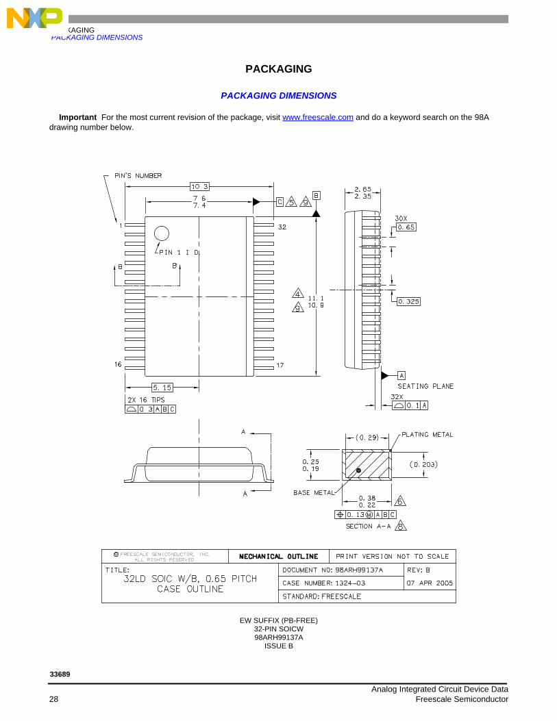
PACKAGINGPACKAGING DIMENSIONS
PACKAGING
PACKAGING DIMENSIONS
Important For the most current revision of the package, visit www.freescale.com and do a keyword search on the 98A drawing number below.
EW SUFFIX (PB-FREE)32-PIN SOICW98ARH99137A
ISSUE B
Analog Integrated Circuit Device Data 28 Freescale Semiconductor
33689

PACKAGINGPACKAGING DIMENSIONS (CONTINUED)
PACKAGING DIMENSIONS (CONTINUED)
EW SUFFIX (PB-FREE)32-PIN SOICW98ARH99137A
ISSUE B
Analog Integrated Circuit Device Data Freescale Semiconductor 29
33689

Analog Integrated Circuit Device Data 30 Freescale Semiconductor
33689
REVISION HISTORY
REVISION HISTORY
REVISION DATE DESCRIPTION OF CHANGES
6.0 6/2006 • Implemented Revision History page• Updated Outline Drawing to Revision “B”• Eliminated all pages (pages 30 to 47) referring to the MC33689DWB/R2 device• Removed MC33689DWB/R2 from the orderable parts information• Updated to the prevailing form and style
7.0 8/2006 • Removed MC33689DEW/R2 and replaced with MCZ33689DEW/R2 in the Ordering Information block
8.0 9/2012 • Updated orderable part number from MC33689DEW to MC33689DPEW• Removed MCZ33689DPEW• Removed DWB suffix from drawing info• Updated Freescale form and style

Document Number: MC33689Rev. 8.09/2012
Information in this document is provided solely to enable system and software implementers to
use Freescale products. There are no express or implied copyright licenses granted hereunder to
design or fabricate any integrated circuits based on the information in this document.
Freescale reserves the right to make changes without further notice to any products herein.
Freescale makes no warranty, representation, or guarantee regarding the suitability of its
products for any particular purpose, nor does Freescale assume any liability arising out of the
application or use of any product or circuit, and specifically disclaims any and all liability,
including without limitation consequential or incidental damages. “Typical” parameters that
may be provided in Freescale data sheets and/or specifications can and do vary in different
applications, and actual performance may vary over time. All operating parameters, including
“typicals,” must be validated for each customer application by customer’s technical experts.
Freescale does not convey any license under its patent rights nor the rights of others. Freescale
sells products pursuant to standard terms and conditions of sale, which can be found at the
following address: store.esellerate.net/store/
Policy.aspx?Selector=RT&s=STR0326182960&pc.
How to Reach Us:Home Page: freescale.com
Web Support: freescale.com/support
Freescale, the Freescale logo, AltiVec, C-5, CodeTest, CodeWarrior, ColdFire, C-Ware, Energy
Efficient Solutions logo, Kinetis, mobileGT, PowerQUICC, Processor Expert, QorIQ, Qorivva,
StarCore, Symphony, and VortiQa are trademarks of Freescale Semiconductor, Inc., Reg. U.S.
Pat. & Tm. Off. Airfast, BeeKit, BeeStack, ColdFire+, CoreNet, Flexis, MagniV, MXC,
Platform in a Package, QorIQ Qonverge, QUICC Engine, Ready Play, SafeAssure,
SMARTMOS, TurboLink, Vybrid, and Xtrinsic are trademarks of Freescale Semiconductor,
Inc. All other product or service names are the property of their respective owners.
© 2012 Freescale Semiconductor, Inc.