Embed Size (px)
Citation preview
Multi-Gigabit Serial Link Transmitter- Off-Chip and On-Chip
Shyh-Jye Jou Department of Electronics Engineering,
National Chiao Tung University, Taiwan 300, R.O.C.
Chih-Hsien Lin, Chih-Ning Chen, You-Jiun Wang and Ju-Yuan Hsiao
Department of Electrical Engineering National Central University, Taiwan 320, R.O.C,
Abstract - Multi-Gbps serial link transmitter for both off-chip and on-chip transmission are presented. For off-chip transmission, a new pre-emphasis design methodology and circuits for a 4/2 PAM transmitter over cable are proposed. A test chip of transmitter with pre-emphasis, PLL circuit and on-chip termination resistors is implemented using tsmc 0.18 um CMOS process. The measurement results of 10/5 Gbps (4/2 PAM) are carried out over 5 meter (m) long cable and is in agreement with our analysis and simulation results. For on-chip transmission, SerDes based serial link architecture is used in on-chip application. Using tsmc 0.13 um CMOS process, the operation speed and power consumption are 5 Gbps and 3.2 mW respectively with the interconnect area is half of parallel architecture.
I. Introduction With the data rate up to several Gbps over cable of several
meters or on-chip interconnect of several thousands micrometer, the propagation of the signaling is affected by two limitations. The first limitation is due to the circuit performance and the second limitation is the bandwidth of transmission channel. The chip package parasitic components dominate the output pin performance because of the pin’s loading and bonding wire. The RC time constant of pin lowers the location of the -3dB frequency. The inductance of bonding wire (several nH) results in a pattern dependent data jitter and lowers the signal to noise ratio. The attenuation of cable increases with cable length and frequency. Therefore, pre-emphasis in transmitters [1-5] have been adopted to compensate for the distortion. Usually, pre-emphasis is implemented by using high-pass filter with data controlled current source. With less than 1 ns bit time, the distortion compensation of pre-emphasis shall be more precisely. On the other hand, for on-chip transmission, with the feature size is around 50nm, the local clock frequencies are around 10GHz in the end of this decade [2]. When technology is scaling down, the delay on wires will dominate the performance of the chip instead of by gate delay. However, the global wires spanning in the whole chip will carry signals whose propagation delay maybe exceed the local clock period. Thus, on-chip interconnects that transmit signals between modules limit the performance of chip due to long wire delay, large areas, large power consumption and high interconnect complexity.
In order to gain higher data rates without increasing of symbol rate, we apply four level pulse amplitude modulation (4 PAM) [1] to off-chip transmission. Furthermore, we propose a new pre-emphasis architecture and algorithm that can enlarge the high frequency response, so the overall
frequency response in the receiver side is uniform within the desired frequency range. For on-chip transmission, we are the first one to use a Serialization and De-serialization (SerDes) based serial link transceiver. Comparisons are made with transmitters with and without SerDes methods. The paper is organized as follows. Section II shows the analysis, design and implementation of the off-chip cable transmitter. Section III gives the analysis, design and implementation of on-chip interconnect transmitter. Finally, a conclusion is made in section IV.
II. Off-Chip Transmitter over Cable A. Architecture
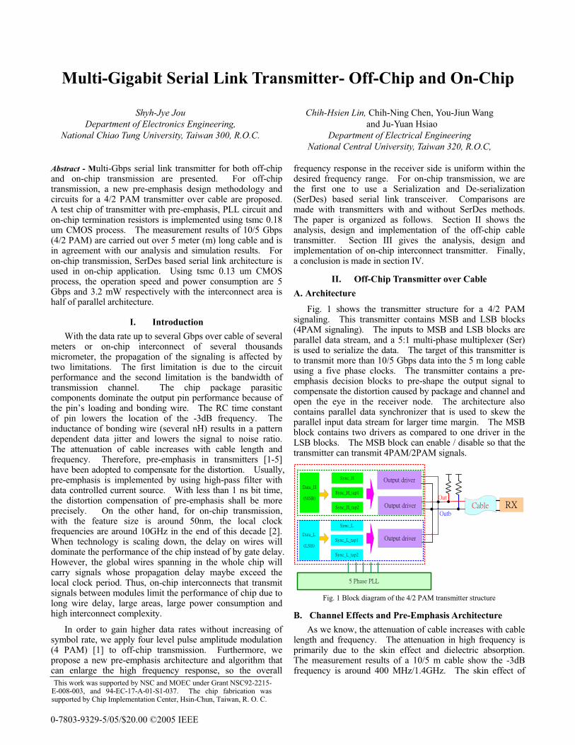
Fig. 1 shows the transmitter structure for a 4/2 PAM signaling. This transmitter contains MSB and LSB blocks (4PAM signaling). The inputs to MSB and LSB blocks are parallel data stream, and a 5:1 multi-phase multiplexer (Ser) is used to serialize the data. The target of this transmitter is to transmit more than 10/5 Gbps data into the 5 m long cable using a five phase clocks. The transmitter contains a pre-emphasis decision blocks to pre-shape the output signal to compensate the distortion caused by package and channel and open the eye in the receiver node. The architecture also contains parallel data synchronizer that is used to skew the parallel input data stream for larger time margin. The MSB block contains two drivers as compared to one driver in the LSB blocks. The MSB block can enable / disable so that the transmitter can transmit 4PAM/2PAM signals.
Fig. 1 Block diagram of the 4/2 PAM transmitter structure
B. Channel Effects and Pre-Emphasis Architecture As we know, the attenuation of cable increases with cable
length and frequency. The attenuation in high frequency is primarily due to the skin effect and dielectric absorption. The measurement results of a 10/5 m cable show the -3dB frequency is around 400 MHz/1.4GHz. The skin effect of
This work was supported by NSC and MOEC under Grant NSC92-2215-E-008-003, and 94-EC-17-A-01-S1-037. The chip fabrication was supported by Chip Implementation Center, Hsin-Chun, Taiwan, R. O. C.
0-7803-9329-5/05/$20.00 ©2005 IEEE
cable distorts the signaling because the attenuation of the low frequency and high frequency is not uniform.
The frequency response of cable behaves like a low pass function. Pre-emphasis circuit plays a role of high pass filter. Thus in the receiver the frequency response is flattened within the bandwidth of our desired frequency range. The pre-emphasis using a Finite Impulse Response (FIR) filter can either amplify the high frequency component or attenuate the low frequency component [1]. One method enlarges the high frequency component as shown in Eqn. (1). The other method [1] mainly suppresses the low frequency component as shown in Eqn.(2).
1
10 )()(*)1()(
N
iiniino inVanVanV
(1) 1
1)()(*1)(
N
iniiino inVanVnV
(2) In Eqn.(1) and (2), Vin(n-i) is an input data sequence with i=0,1,2…. as time index of a bit time, ai and bi are taps coefficients. In here, previous data are used. A long tail (serious post-ISI) will need more taps (N larger) to cancel it.
In our method, we keep a0 equals to (a1+a2+…+aN-1) to have constant DC amplitude. The advantage of our method is that we have constant receiver signal amplitude even for a different cable length but it needs to decide one more coefficient (a0). On the other hand, the disadvantage of other method has different signal amplitudes in receiver node for different cable length. According to Eqn.(2), we can derivate the coefficient of each tap as shown in Fig.2 for N=3. We can implement the pre-emphasis using the current source circuits in the driver and use a shift register to produce delay chain of bits [2-5]. Tap1 and tap2 are controlled by the input data that are delayed one bit and two bits. We can adjust a0, a1 and a2 (the current in main, tap1 and tap2 drivers) so that signal amplitude in the receiver is the same for different cable length. Also in this proposed tuning scheme, the maximum transmit amplitude for both the differential lines are the same.
Fig. 2 Main driver and pre-emphasis architecture
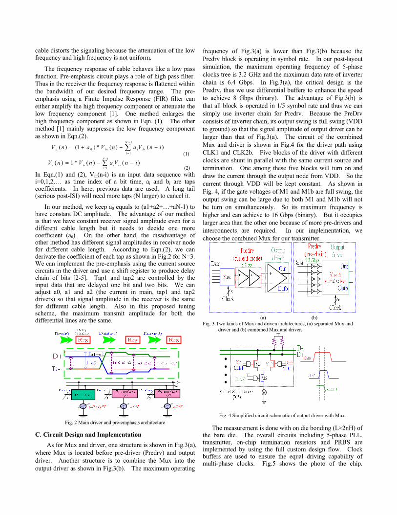
C. Circuit Design and Implementation As for Mux and driver, one structure is shown in Fig.3(a),
where Mux is located before pre-driver (Predrv) and output driver. Another structure is to combine the Mux into the output driver as shown in Fig.3(b). The maximum operating
frequency of Fig.3(a) is lower than Fig.3(b) because the Predrv block is operating in symbol rate. In our post-layout simulation, the maximum operating frequency of 5-phase clocks tree is 3.2 GHz and the maximum data rate of inverter chain is 6.4 Gbps. In Fig.3(a), the critical design is the Predrv, thus we use differential buffers to enhance the speed to achieve 8 Gbps (binary). The advantage of Fig.3(b) is that all block is operated in 1/5 symbol rate and thus we can simply use inverter chain for Predrv. Because the PreDrv consists of inverter chain, its output swing is full swing (VDD to ground) so that the signal amplitude of output driver can be larger than that of Fig.3(a). The circuit of the combined Mux and driver is shown in Fig.4 for the driver path using CLK1 and CLK2b. Five blocks of the driver with different clocks are shunt in parallel with the same current source and termination. One among these five blocks will turn on and draw the current through the output node from VDD. So the current through VDD will be kept constant. As shown in Fig. 4, if the gate voltages of M1 and M1b are full swing, the output swing can be large due to both M1 and M1b will not be turn on simultaneously. So its maximum frequency is higher and can achieve to 16 Gbps (binary). But it occupies larger area than the other one because of more pre-drivers and interconnects are required. In our implementation, we choose the combined Mux for our transmitter.
(a) (b) Fig. 3 Two kinds of Mux and driven architectures, (a) separated Mux and
driver and (b) combined Mux and driver.
Fig. 4 Simplified circuit schematic of output driver with Mux.
The measurement is done with on die bonding (L 2nH) of the bare die. The overall circuits including 5-phase PLL, transmitter, on-chip termination resistors and PRBS are implemented by using the full custom design flow. Clock buffers are used to ensure the equal driving capability of multi-phase clocks. Fig.5 shows the photo of the chip.
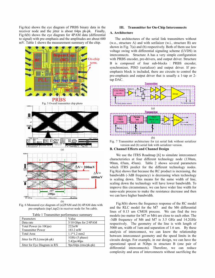
Fig.6(a) shows the eye diagram of PRBS binary data in the receiver node and the jitter is about 64ps pk-pk. Finally, Fig.6(b) shows the eye diagram for 4PAM data (differential to signal) with pre-emphasis and the amplitudes are about 600 mV. Table 1 shows the measurement summary of the chip.
Fig. 5 Overall transmitter chip photo
(a)
(b) Fig. 6 Measured eye diagram of (a)2PAM and (b) 4PAM data with
pre-emphasis (tap1,tap2) in receiver node for 5m cable.
Table 1 Transmitter performance summary Parameters Value Data rate 5/10 Gbps for 2/4PAM Total Power (in 10Gps) Transmitter Power
222mW183.2 mW
Total Area 1.1*1.2 mm2
Jitter for PLL(rms/pk-pk) 1GHz (5 phase) 5.42ps/40ps
Jitter for Eye Diagram in RX 9ps/64ps (rms/pk-pk)
III. Transmitter for On-Chip Interconnects A. Architecture
The architectures of the serial link transmitters without (w.o., structure A) and with serilaizer (w.i., structure B) are shown in Fig. 7(a) and (b) respectively. Both of them use low voltage swing with differential signaling scheme (LVDS) in interconnects. Structure A has a very simple configuration with PRBS encoder, pre-drivers, and output driver. Structure B is composed of four sub-blocks PRBS encoder, synchronizer, PISO (serializer) and output driver. If pre-emphasis block is included, there are circuits to control the pre-emphasis and output driver that is usually a 1-tap or 2-tap DAC.
Driver
Data in
Transmitter
To interconnects
4-bits PRBS encoder
Clock phase source
(a)
(b)
Fig. 7 Transmitter architecture for (a) serial link without serializer version and (b) serial link with serializer version.
B. Channel Effects and Channel Design
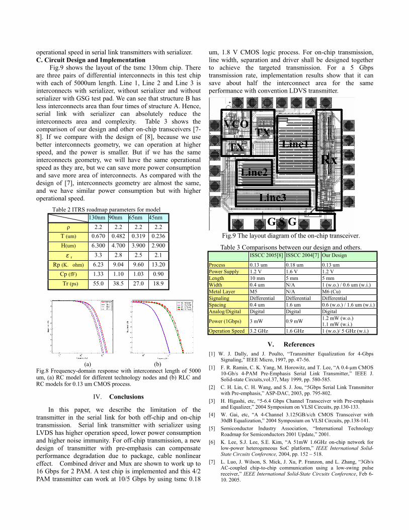
We use the ITRS Roadmap [6] to simulate interconnect characteristics at four different technology node (130nm, 90nm, 65nm, 45nm). Table 2 shows several parameters which ITRS predict for the different technology nodes. Fig.8(a) shows that because the RC product is increasing, the bandwidth (-3dB frequency) is decreasing when technology is scaling down. This means for the same width of line, scaling down the technology will have lower bandwidth. To improve this circumstance, we can have wider line width for nano-scale process to make the resistance decrease and then we can have higher bandwidth.
Fig.8(b) shows the frequency response of the RC model and the RLC model for the M7 and the M6 differential lines of 0.13 um CMOS process. We can find the two models (no matter for M7 or M6) are close to each other. The -3dB frequency of M6 and M7 is 3.5 GHz and 14.2GHz respectively. The geometry of the line is with length of 5000 um, width of 1um and separation of 1.6 um. By these analysis of interconnect, we can know the relationship between interconnect geometry and the speed limits in the circuits design. For example, in our design, we can have the operational speed at 5Gbps in structure B (one pair of differential interconnects). Therefore, we can reduce complexity and area of interconnects without sacrificing the
operational speed in serial link transmitters with serializer. C. Circuit Design and Implementation
Fig.9 shows the layout of the tsmc 130nm chip. There are three pairs of differential interconnects in this test chip with each of 5000um length. Line 1, Line 2 and Line 3 is interconnects with serializer, without serializer and without serializer with GSG test pad. We can see that structure B has less interconnects area than four times of structure A. Hence, serial link with serializer can absolutely reduce the interconnects area and complexity. Table 3 shows the comparison of our design and other on-chip transceivers [7-8]. If we compare with the design of [8], because we use better interconnects geometry, we can operation at higher speed, and the power is smaller. But if we has the same interconnects geometry, we will have the same operational speed as they are, but we can save more power consumption and save more area of interconnects. As compared with the design of [7], interconnects geometry are almost the same, and we have similar power consumption but with higher operational speed.
Table 2 ITRS roadmap parameters for model 130nm 90nm 65nm 45nm
2.2 2.2 2.2 2.2 T (um) 0.670 0.482 0.319 0.236H(um) 6.300 4.700 3.900 2.900
r 3.3 2.8 2.5 2.1 Rp (K ohm) 6.23 9.04 9.60 13.20
Cp (fF) 1.33 1.10 1.03 0.90 Tr (ps) 55.0 38.5 27.0 18.9
(a) (b) Fig.8 Frequency-domain response with interconnect length of 5000 um, (a) RC model for different technology nodes and (b) RLC and RC models for 0.13 um CMOS process.
IV. Conclusions
In this paper, we describe the limitation of the transmitter in the serial link for both off-chip and on-chip transmission. Serial link transmitter with serializer using LVDS has higher operation speed, lower power consumption and higher noise immunity. For off-chip transmission, a new design of transmitter with pre-emphasis can compensate performance degradation due to package, cable nonlinear effect. Combined driver and Mux are shown to work up to 16 Gbps for 2 PAM. A test chip is implemented and this 4/2 PAM transmitter can work at 10/5 Gbps by using tsmc 0.18
um, 1.8 V CMOS logic process. For on-chip transmission, line width, separation and driver shall be designed together to achieve the targeted transmission. For a 5 Gbps transmission rate, implementation results show that it can save about half the interconnect area for the same performance with convention LDVS transmitter.
Fig.9 The layout diagram of the on-chip transceiver.
Table 3 Comparisons between our design and others. ISSCC 2005[8] ISSCC 2004[7] Our Design
Process 0.13 um 0.18 um 0.13 um Power Supply 1.2 V 1.6 V 1.2 V Length 10 mm 5 mm 5 mm Width 0.4 um N/A 1 (w.o.) / 0.6 um (w.i.) Metal Layer M5 N/A M6 (Cu) Signaling Differential Differential Differential Spacing 0.4 um 1.6 um 0.6 (w.o.) / 1.6 um (w.i.)Analog/Digital Digital Digital Digital
Power (1Gbps) 3 mW 0.9 mW 1.2 mW (w.o.) 1.1 mW (w.i.)
Operation Speed 3.2 GHz 1.6 GHz 1 (w.o.)/ 5 GHz (w.i.)
V. References [1] W. J. Dally, and J. Poulto, “Transmitter Equalization for 4-Gbps
Signaling,” IEEE Micro, 1997, pp. 47-56. [1] F. R. Ramin, C. K. Yang, M. Horowitz, and T. Lee, “A 0.4- m CMOS
10-Gb/s 4-PAM Pre-Emphasis Serial Link Transmitter,” IEEE J. Solid-state Circuits,vol.37, May 1999, pp. 580-585.
[2] C. H. Lin, C. H. Wang, and S. J. Jou, “5Gbps Serial Link Transmitter with Pre-emphasis,” ASP-DAC, 2003, pp. 795-802.
[3] H. Higashi, etc, “5-6.4 Gbps Channel Transceiver with Pre-emphasis and Equalizer,” 2004 Symposium on VLSI Circuits, pp.130-133.
[4] W. Gai, etc, “A 4-Channel 3.125GB/s/ch CMOS Transceiver with 30dB Equalization,” 2004 Symposium on VLSI Circuits, pp.138-141.
[5] Semiconductor Industry Association, “International Technology Roadmap for Semiconductors 2001 Update,” 2001.
[6] K. Lee, S.J. Lee, S.E. Kim, “A 51mW 1.6GHz on-chip network for low-power heterogeneous SoC platform,” IEEE International Solid-State Circuits Conference, 2004, pp. 152 – 518.
[7] L. Luo, J. Wilson, S. Mick, J. Xu, P. Franzon, and L. Zhang, “3Gb/s AC-coupled chip-to-chip communication using a low-swing pulse receiver,” IEEE International Solid-State Circuits Conference, Feb 6-10. 2005.