Embed Size (px)
Citation preview

DCT OR DCU PACKAGE
(TOP VIEW)
1
2
3
4
8
7
6
5
VCCA
A1
A2
GND
VCCB
B1
B2
DIR
SN74LVC2T45-EP
www.ti.com SCES777C –NOVEMBER 2008–REVISED JULY 2010
DUAL-BIT DUAL-SUPPLY BUS TRANSCEIVERWITH CONFIGURABLE VOLTAGE TRANSLATION AND 3-STATE OUTPUTS
Check for Samples: SN74LVC2T45-EP
1FEATURES• Available in the Texas Instruments NanoFree™ SUPPORTS DEFENSE, AEROSPACE,
Package AND MEDICAL APPLICATIONS• Controlled Baseline• Fully Configurable Dual-Rail Design Allows
Each Port to Operate Over the Full 1.65-V to • One Assembly/Test Site5.5-V Power-Supply Range • One Fabrication Site
• VCC Isolation Feature – If Either VCC Input Is at • Available Temperature Ranges:GND, Both Ports Are in the High-Impedance – –55°C to 125°CState – –55°C to 150°C
• DIR Input Circuit Referenced to VCCA • Extended Product Life Cycle• Low Power Consumption, 10-mA Max ICC • Extended Product-Change Notification• ±24-mA Output Drive at 3.3 V • Product Traceability• Ioff Supports Partial-Power-Down Mode
Operation• Max Data Rates
– 420 Mbps (3.3-V to 5-V Translation)– 210 Mbps (Translate to 3.3 V)– 140 Mbps (Translate to 2.5 V)– 75 Mbps (Translate to 1.8 V)
• Latch-Up Performance Exceeds 100 mA PerJESD 78, Class II
• ESD Protection Exceeds JESD 22– 4000-V Human-Body Model (A114-A)– 200-V Machine Model (A115-A)– 1000-V Charged-Device Model (C101)
DESCRIPTION/ORDERING INFORMATIONThis dual-bit noninverting bus transceiver uses two separate configurable power-supply rails. The A port isdesigned to track VCCA. VCCA accepts any supply voltage from 1.65 V to 5.5 V. The B port is designed to trackVCCB. VCCB accepts any supply voltage from 1.65 V to 5.5 V. This allows for universal low-voltage bidirectionaltranslation between any of the 1.8-V, 2.5-V, 3.3-V, and 5-V voltage nodes.
Table 1. ORDERING INFORMATION (1)
TA PACKAGE (2) ORDERABLE PART NUMBER TOP-SIDE MARKING
–55°C to 125°C SSOP – DCT Reel of 250 SN74LVC2T45MDCTTEP NXR
–55°C to 150°C SSOP – DCU Reel of 250 SN74LVC2T45SDCUT CCVR
(1) For the most current package and ordering information, see the Package Option Addendum at the end of this document, or see the TIwebsite at www.ti.com.
(2) Package drawings, standard packing quantities, thermal data, symbolization, and PCB design guidelines are available atwww.ti.com/sc/package.
1
Please be aware that an important notice concerning availability, standard warranty, and use in critical applications of TexasInstruments semiconductor products and disclaimers thereto appears at the end of this data sheet.
PRODUCTION DATA information is current as of publication date. Copyright © 2008–2010, Texas Instruments IncorporatedProducts conform to specifications per the terms of the TexasInstruments standard warranty. Production processing does notnecessarily include testing of all parameters.

B1
DIR5
7
A12
VCCA VCCB
B26
A23
SN74LVC2T45-EP
SCES777C –NOVEMBER 2008–REVISED JULY 2010 www.ti.com
DESCRIPTION/ORDERING INFORMATION (CONTINUED)The SN74LVC2T45 is designed for asynchronous communication between two data buses. The logic levels ofthe direction-control (DIR) input activate either the B-port outputs or the A-port outputs. The device transmits datafrom the A bus to the B bus when the B-port outputs are activated, and from the B bus to the A bus when theA-port outputs are activated. The input circuitry on both A and B ports always is active and must have a logicHIGH or LOW level applied to prevent excess ICC and ICCZ.
The SN74LVC2T45 is designed so that the DIR input circuit is supplied by VCCA.
This device is fully specified for partial-power-down applications using Ioff. The Ioff circuitry disables the outputs,preventing damaging current backflow through the device when it is powered down.
The VCC isolation feature ensures that if either VCC input is at GND, both ports are in the high-impedance state.
NanoFree™ package technology is a major breakthrough in IC packaging concepts, using the die as thepackage.
Table 2. FUNCTION TABLE (1)
(EACH TRANSCEIVER)
INPUT OPERATIONDIR
L B data to A bus
H A data to B bus
(1) Input circuits of the data I/Osalways are active.
LOGIC DIAGRAM (POSITIVE LOGIC)
2 Submit Documentation Feedback Copyright © 2008–2010, Texas Instruments Incorporated
Product Folder Link(s): SN74LVC2T45-EP
SN74LVC2T45-EP
www.ti.com SCES777C –NOVEMBER 2008–REVISED JULY 2010
Absolute Maximum Ratings (1)
over operating free-air temperature range (unless otherwise noted)
MIN MAX UNIT
VCCASupply voltage range –0.5 6.5 V
VCCB
VI Input voltage range (2) –0.5 6.5 V
VO Voltage range applied to any output in the high-impedance or power-off state (2) –0.5 6.5 V
A port –0.5 VCCA + 0.5VO Voltage range applied to any output in the high or low state (2) (3) V
B port –0.5 VCCB + 0.5
IIK Input clamp current VI < 0 –50 mA
IOK Output clamp current VO < 0 –50 mA
IO Continuous output current ±50 mA
Continuous current through VCC or GND ±100 mA
DCT 220qJA Package thermal impedance (4) °C/W
DCU 329.4
Tstg Storage temperature range –65 150 °C
(1) Stresses beyond those listed under "absolute maximum ratings" may cause permanent damage to the device. These are stress ratingsonly, and functional operation of the device at these or any other conditions beyond those indicated under "recommended operatingconditions" is not implied. Exposure to absolute-maximum-rated conditions for extended periods may affect device reliability.
(2) The input and output negative-voltage ratings may be exceeded if the input and output clamp-current ratings are observed.(3) The value of VCC is provided in the recommended operating conditions table.(4) The package thermal impedance is calculated in accordance with JESD 51-7.
Copyright © 2008–2010, Texas Instruments Incorporated Submit Documentation Feedback 3
Product Folder Link(s): SN74LVC2T45-EP
SN74LVC2T45-EP
SCES777C –NOVEMBER 2008–REVISED JULY 2010 www.ti.com
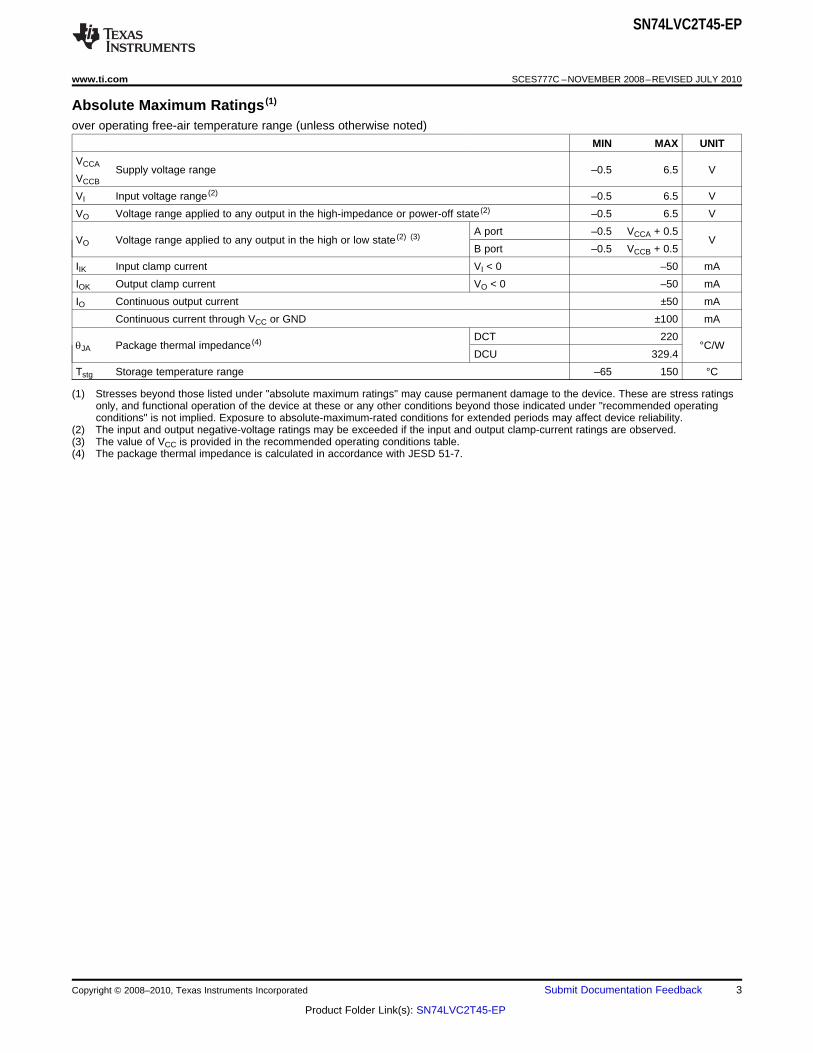
Recommended Operating Conditions (1) (2) (3)
VCCI VCCO MIN MAX UNIT
VCCA 1.65 5.5Supply voltage V
VCCB 1.65 5.5
1.65 V to 1.95 V VCCI × 0.65
2.3 V to 2.7 V 1.7High-levelVIH Data inputs (4) Vinput voltage 3 V to 3.6 V 2
4.5 V to 5.5 V VCCI × 0.7
1.65 V to 1.95 V VCCI × 0.35
2.3 V to 2.7 V 0.7Low-levelVIL Data inputs (4) Vinput voltage 3 V to 3.6 V 0.8
4.5 V to 5.5 V VCCI × 0.3
1.65 V to 1.95 V VCCA × 0.65
2.3 V to 2.7 V 1.7High-level DIRVIH Vinput voltage (referenced to VCCA) (5)3 V to 3.6 V 2
4.5 V to 5.5 V VCCA × 0.7
1.65 V to 1.95 V VCCA × 0.35
2.3 V to 2.7 V 0.7Low-level DIRVIL Vinput voltage (referenced to VCCA)(5)3 V to 3.6 V 0.8
4.5 V to 5.5 V VCCA × 0.3
VI Input voltage 0 5.5 V
VO Output voltage 0 VCCO V
1.65 V to 1.95 V –4
2.3 V to 2.7 V –8IOH High-level output current mA
3 V to 3.6 V –24
4.5 V to 5.5 V –32
1.65 V to 1.95 V 4
2.3 V to 2.7 V 8IOL Low-level output current mA
3 V to 3.6 V 24
4.5 V to 5.5 V 32
1.65 V to 1.95 V 20
2.3 V to 2.7 V 20Data inputsInput transitionΔt/Δv 3 V to 3.6 V 10 ns/Vrise or fall rate
4.5 V to 5.5 V 5
Control input 1.65 V to 5.5 V 5
DCT –55 125Operating free-airTA °Ctemperature DCU –55 150
(1) VCCI is the VCC associated with the input port.(2) VCCO is the VCC associated with the output port.(3) All unused data inputs of the device must be held at VCCI or GND to ensure proper device operation. Refer to the TI application report,
Implications of Slow or Floating CMOS Inputs, literature number SCBA004.(4) For VCCI values not specified in the data sheet, VIH min = VCCI × 0.7 V, VIL max = VCCI × 0.3 V.(5) For VCCI values not specified in the data sheet, VIH min = VCCA × 0.7 V, VIL max = VCCA × 0.3 V.
4 Submit Documentation Feedback Copyright © 2008–2010, Texas Instruments Incorporated
Product Folder Link(s): SN74LVC2T45-EP

SN74LVC2T45-EP
www.ti.com SCES777C –NOVEMBER 2008–REVISED JULY 2010
Electrical Characteristics (1) (2)
over recommended operating free-air temperature range (unless otherwise noted)TA = 25°C –55°C to 125°C –55°C to 150°C
PARAMETER TEST CONDITIONS VCCA VCCB UNITTYP MAX MIN MAX MIN MAX
IOH = –100 mA 1.65 V to 4.5 V 1.65 V to 4.5 V VCCO – 0.1 VCCO – 0.1
IOH = –4 mA 1.65 V 1.65 V 1.2 1.2
VOH IOH = –8 mA VI = VIH 2.3 V 2.3 V 1.9 1.9 V
IOH = –24 mA 3 V 3 V 2.4 2.4
IOH = –32 mA 4.5 V 4.5 V 3.8 3.8
IOL = 100 mA 1.65 V to 4.5 V 1.65 V to 4.5 V 0.1 0.1
IOL = 4 mA 1.65 V 1.65 V 0.45 0.45
VOL IOL = 8 mA VI = VIL 2.3 V 2.3 V 0.3 0.3 V
IOL = 24 mA 3 V 3 V 0.55 0.55
IOL = 32 mA 4.5 V 4.5 V 0.55 0.55
II DIR VI = VCCA or GND 1.65 V to 5.5 V 1.65 V to 5.5 V ±1 ±2 ±2 mA
A port 0 V 0 to 5.5 V ±1 ±9 ±9Ioff VI or VO = 0 to 5.5 V mA
B port 0 to 5.5 V 0 V ±1 ±9 ±9
A orIOZ VO = VCCO or GND 1.65 V to 5.5 V 1.65 V to 5.5 V ±1 ±9 ±9 mAB port
1.65 V to 5.5 V 1.65 V to 5.5 V 4 4VI = VCCI orICCA IO = 0 5 V 0 V 2 2 mAGND,
0 V 5 V –12 –12
1.65 V to 5.5 V 1.65 V to 5.5 V 4 4VI = VCCI orICCB IO = 0 5 V 0 V –12 –12 mAGND,
0 V 5 V 2 2
ICCA + ICCB VI = VCCI or IO = 0 1.65 V to 5.5 V 1.65 V to 5.5 V 4 4 mA(see Table 3) GND,
One A port at VCCA – 0.6 V,A port DIR at VCCA, 50 50
B port = openΔICCA 3 V to 5.5 V 3 V to 5.5 V mA
DIR at VCCA – 0.6 V,DIR B port = open, 50 50
A port at VCCA or GND
One B port at VCCB – 0.6 V,ΔICCB B port 3 V to 5.5 V 3 V to 5.5 V 50 50 mADIR at GND, A port = open
CI DIR VI = VCCA or GND 3.3 V 3.3 V 2.5 pF
A orCio VO = VCCA/B or GND 3.3 V 3.3 V 6 pFB port
(1) VCCO is the VCC associated with the output port.(2) VCCI is the VCC associated with the input port.
Copyright © 2008–2010, Texas Instruments Incorporated Submit Documentation Feedback 5
Product Folder Link(s): SN74LVC2T45-EP

Notes:
1. See datasheet for absolute maximum and minimum recommended operating conditions.
2. Silicon operating life design goal is 10 years at 105°C junction temperature (does not include package interconnect life).
3. Product disclaimer applies to DCU package 150°C.
0.10
1.00
10.00
100.00
1000.00
80 90 100 110 120 130 140 150 160 170 180
Continuous TA (°C)
Esti
mate
dL
ife
(Years
)
Wirebond Voiding Fail Mode
Electromigration Fail Mode
SN74LVC2T45-EP
SCES777C –NOVEMBER 2008–REVISED JULY 2010 www.ti.com
Figure 1. LVC2T45SDCU Operating Life Derating Chart
6 Submit Documentation Feedback Copyright © 2008–2010, Texas Instruments Incorporated
Product Folder Link(s): SN74LVC2T45-EP

SN74LVC2T45-EP
www.ti.com SCES777C –NOVEMBER 2008–REVISED JULY 2010
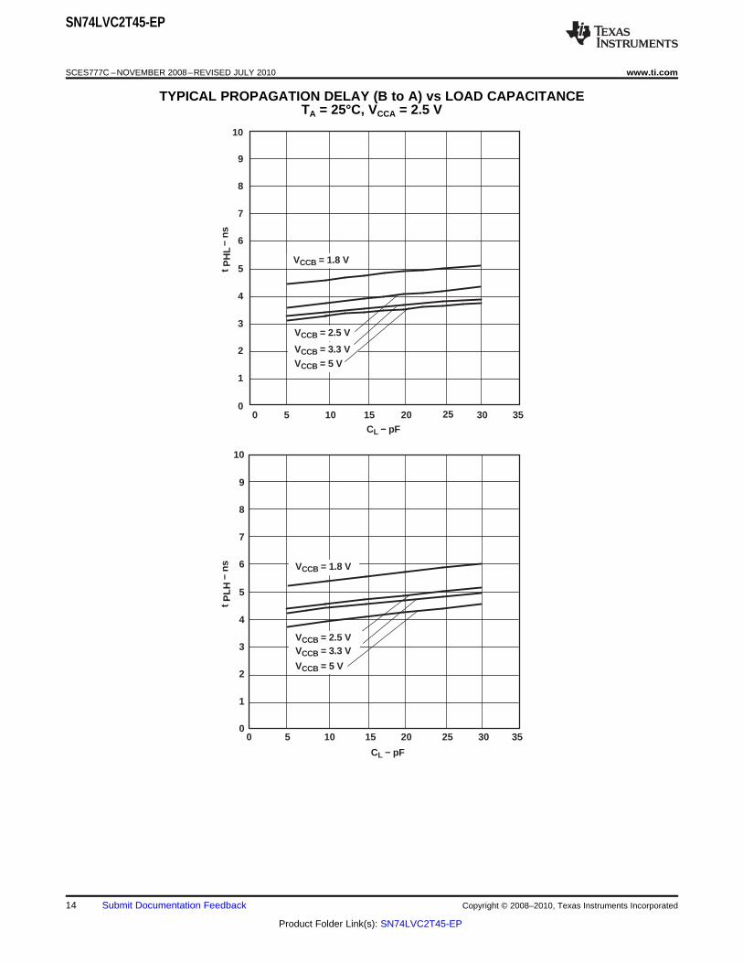
Switching Characteristicsover recommended operating free-air temperature range, VCCA = 1.8 V ± 0.15 V (unless otherwise noted) (see Figure 2)
VCCB = 1.8 V VCCB = 2.5 V VCCB = 3.3 V VCCB = 5 VFROM TO ±0.15 V ±0.2 V ±0.3 V ±0.5 VPARAMETER UNIT(INPUT) (OUTPUT)
MIN MAX MIN MAX MIN MAX MIN MAX
tPLH 3 21.7 2.2 14.3 1.7 12.3 1.4 11.2A B ns
tPHL 2.8 28.3 2.2 12.5 1.8 11.1 1.7 11
tPLH 3 21.7 2.3 20 2.1 19.5 1.9 19.1B A ns
tPHL 2.8 18.3 2.1 16.9 2 16.6 1.8 16.2
tPHZ 10.6 34.9 10.3 34.5 10.5 34.5 10.7 33.3DIR A ns
tPLZ 7.3 23.7 7.5 23.6 7.5 23.5 7 23.4
tPHZ 10 31.9 8.4 18.9 6.5 15.3 4.1 12.6DIR B ns
tPLZ 6.5 23.5 7.2 16.6 4.3 13.7 2.1 11.1
tPZH(1) 45.2 36.6 33.2 30.2
DIR A nstPZL
(1) 50.2 35.8 31.9 28.8
tPZH(1) 45.4 37.9 35.8 34.6
DIR B nstPZL
(1) 53.2 47 45.6 44.3
(1) The enable time is a calculated value, derived using the formula shown in the enable times section.
Switching Characteristicsover recommended operating free-air temperature range, VCCA = 2.5 V ± 0.2 V (unless otherwise noted) (see Figure 2)
VCCB = 1.8 V VCCB = 2.5 V VCCB = 3.3 V VCCB = 5 VFROM TO ±0.15 V ±0.2 V ±0.3 V ±0.5 VPARAMETER UNIT(INPUT) (OUTPUT)
MIN MAX MIN MAX MIN MAX MIN MAX
tPLH 2.3 20 1.5 12.5 1.3 10.4 1.1 9.1A B ns
tPHL 2.1 16.9 1.4 11.5 1.3 9.4 0.9 8.6
tPLH 2.2 14.3 1.5 12.5 1.4 12 1 11.5B A ns
tPHL 2.2 12.5 1.4 11.5 1.3 11 0.9 10.2
tPHZ 6.6 21.1 7.1 20.8 6.8 20.8 5.2 20.5DIR A ns
tPLZ 5.3 16.6 5.2 16.5 4.9 16.3 4.8 16.3
tPHZ 10.7 31.9 8.1 17.9 5.8 14.5 3.5 11.6DIR B ns
tPLZ 7.8 22.9 6.2 15.2 3.6 12.9 1.4 11.2
tPZH(1) 37.2 27.7 24.9 21.7
DIR A nstPZL
(1) 44.4 29.4 25.5 21.8
tPZH(1) 26.6 29 26.7 25.4
DIR B nstPZL
(1) 38 32.3 30.2 29.1
(1) The enable time is a calculated value, derived using the formula shown in the enable times section.
Copyright © 2008–2010, Texas Instruments Incorporated Submit Documentation Feedback 7
Product Folder Link(s): SN74LVC2T45-EP

SN74LVC2T45-EP
SCES777C –NOVEMBER 2008–REVISED JULY 2010 www.ti.com
Switching Characteristicsover recommended operating free-air temperature range, VCCA = 3.3 V ± 0.3 V (unless otherwise noted) (see Figure 2)
VCCB = 1.8 V VCCB = 2.5 V VCCB = 3.3 V VCCB = 5 VFROM TO ±0.15 V ±0.2 V ±0.3 V ±0.5 VPARAMETER UNIT(INPUT) (OUTPUT)
MIN MAX MIN MAX MIN MAX MIN MAX
tPLH 2.1 19.5 1.4 12 0.7 9.6 0.7 8.4A B ns
tPHL 2 16.6 1.3 11 0.8 9 0.7 8
tPLH 1.7 12.3 1.3 10.4 0.7 9.8 0.6 9.4B A ns
tPHL 1.8 11.1 1.3 9.4 0.8 9 0.7 8.5
tPHZ 5 14.9 5.1 14.8 5 14.8 5 14.4DIR A ns
tPLZ 3.4 12.4 3.7 12.4 3.9 12.1 3.3 11.8
tPHZ 11.2 31.3 8 17.7 5.8 14.4 2.9 11.4DIR B ns
tPLZ 9.4 21.7 5.6 15.3 4.3 12.3 1 9.6
tPZH(1) 34 25.7 22.1 19
DIR A nstPZL
(1) 42.4 27.1 23.4 19.9
tPZH(1) 31.9 24.4 21.9 20.2
DIR B nstPZL
(1) 31.5 25.8 23.8 22.4
(1) The enable time is a calculated value, derived using the formula shown in the enable times section.
Switching Characteristicsover recommended operating free-air temperature range, VCCA = 5 V ± 0.5 V (unless otherwise noted) (see Figure 2)
VCCB = 1.8 V VCCB = 2.5 V VCCB = 3.3 V VCCB = 5 VFROM TO ±0.15 V ±0.2 V ±0.3 V ±0.5 VPARAMETER UNIT(INPUT) (OUTPUT)
MIN MAX MIN MAX MIN MAX MIN MAX
tPLH 1.9 19.1 1 11.5 0.6 9.4 0.5 7.9A B ns
tPHL 1.8 16.2 0.9 10.2 0.7 8.5 0.5 7.5
tPLH 1.4 11.2 1 9.1 0.7 8.4 0.5 7.9B A ns
tPHL 1.7 11 0.9 8.6 0.7 8 0.5 7.5
tPHZ 2.9 12.2 2.9 11.9 2.8 11.9 2.2 11.8DIR A ns
tPLZ 1.4 10.9 1.3 10.7 0.7 10.7 0.7 10.6
tPHZ 11.2 30.1 7.2 17.9 5.8 14.1 1.3 11.3DIR B ns
tPLZ 8.4 20.9 5 15 4 11.7 1 9.6
tPZH(1) 32.1 24.1 20.1 18.5
DIR A nstPZL
(1) 41.1 26.5 22.1 18.8
tPZH(1) 30 22.2 20.1 18.5
DIR B nstPZL
(1) 28.4 22.1 22.4 19.3
(1) The enable time is a calculated value, derived using the formula shown in the enable times section.
8 Submit Documentation Feedback Copyright © 2008–2010, Texas Instruments Incorporated
Product Folder Link(s): SN74LVC2T45-EP

SN74LVC2T45-EP
www.ti.com SCES777C –NOVEMBER 2008–REVISED JULY 2010
Operating CharacteristicsTA = 25°C
VCCA = VCCA = VCCA = VCCA =TEST VCCB = 1.8 V VCCB = 2.5 V VCCB = 3.3 V VCCB = 5 VPARAMETER UNITCONDITIONS
TYP TYP TYP TYP
A-port input, 3 4 4 4CL = 0 pF,B-port outputCpdA
(1) f = 10 MHz, pFB-port input, tr = tf = 1 ns 18 19 20 21A-port output
A-port input, 18 19 20 21CL = 0 pF,B-port outputCpdB
(1) f = 10 MHz, pFB-port input, tr = tf = 1 ns 3 4 4 4A-port output
(1) Power dissipation capacitance per transceiver
Copyright © 2008–2010, Texas Instruments Incorporated Submit Documentation Feedback 9
Product Folder Link(s): SN74LVC2T45-EP
SN74LVC2T45-EP
SCES777C –NOVEMBER 2008–REVISED JULY 2010 www.ti.com
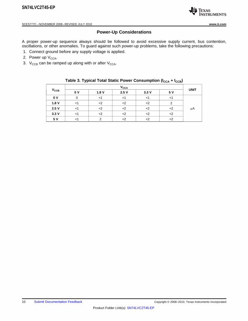
Power-Up Considerations
A proper power-up sequence always should be followed to avoid excessive supply current, bus contention,oscillations, or other anomalies. To guard against such power-up problems, take the following precautions:1. Connect ground before any supply voltage is applied.2. Power up VCCA.3. VCCB can be ramped up along with or after VCCA.
Table 3. Typical Total Static Power Consumption (ICCA + ICCB)
VCCAVCCB UNIT
0 V 1.8 V 2.5 V 3.3 V 5 V
0 V 0 <1 <1 <1 <1
1.8 V <1 <2 <2 <2 2
2.5 V <1 <2 <2 <2 <2 mA
3.3 V <1 <2 <2 <2 <2
5 V <1 2 <2 <2 <2
10 Submit Documentation Feedback Copyright © 2008–2010, Texas Instruments Incorporated
Product Folder Link(s): SN74LVC2T45-EP

0 5 10 15 20 25 30 35
t PH
L −
ns
CL − pF
0
1
2
3
4
5
6
7
8
9
10
VCCB = 1.8 V
VCCB = 2.5 V
VCCB = 3.3 V
VCCB = 5 V
0
1
2
3
4
5
6
7
8
9
10
0 5 10 15 20 25 30 35
t PLH
− n
s
CL − pF
VCCB = 1.8 V
VCCB = 2.5 V
VCCB = 3.3 V
VCCB = 5 V
SN74LVC2T45-EP
www.ti.com SCES777C –NOVEMBER 2008–REVISED JULY 2010
TYPICAL CHARACTERISTICSabc
TYPICAL PROPAGATION DELAY (A to B) vs LOAD CAPACITANCETA = 25°C, VCCA = 1.8 V
Copyright © 2008–2010, Texas Instruments Incorporated Submit Documentation Feedback 11
Product Folder Link(s): SN74LVC2T45-EP

0 5 10 15 20 25 30 35
t PH
L −
ns
CL − pF
VCCB = 1.8 V
VCCB = 2.5 VVCCB = 3.3 V
VCCB = 5 V
0
1
2
3
4
5
6
7
8
9
10
0
1
2
3
4
5
6
7
8
9
10
0 5 10 15 20 25 30 35
t PLH
−
ns
VCCB = 1.8 V
VCCB = 2.5 V
VCCB = 3.3 V
VCCB = 5 V
CL − pF
SN74LVC2T45-EP
SCES777C –NOVEMBER 2008–REVISED JULY 2010 www.ti.com
TYPICAL PROPAGATION DELAY (B to A) vs LOAD CAPACITANCETA = 25°C, VCCA = 1.8 V
12 Submit Documentation Feedback Copyright © 2008–2010, Texas Instruments Incorporated
Product Folder Link(s): SN74LVC2T45-EP

0 5 10 15 20 25 30 35
tP
HL
− ns
CL − pF
0
1
2
3
4
5
6
7
8
9
10
VCCB = 1.8 V
VCCB = 2.5 V
VCCB = 3.3 V
VCCB = 5 V
0
1
2
3
4
5
6
7
8
9
10
0 5 10 15 20 25 30 35
t PLH
−
ns
CL − pF
VCCB = 1.8 V
VCCB = 2.5 V
VCCB = 3.3 V
VCCB = 5 V
SN74LVC2T45-EP
www.ti.com SCES777C –NOVEMBER 2008–REVISED JULY 2010
TYPICAL PROPAGATION DELAY (A to B) vs LOAD CAPACITANCETA = 25°C, VCCA = 2.5 V
Copyright © 2008–2010, Texas Instruments Incorporated Submit Documentation Feedback 13
Product Folder Link(s): SN74LVC2T45-EP
0 5 10 15 20 25 30 35
t PH
L −
ns
CL − pF
0
1
2
3
4
5
6
7
8
9
10
VCCB = 1.8 V
VCCB = 2.5 V
VCCB = 3.3 VVCCB = 5 V
0 5 10 15 20 25 30 35
tP
LH
− ns
CL − pF
0
1
2
3
4
5
6
7
8
9
10
VCCB = 1.8 V
VCCB = 3.3 V
VCCB = 5 V
VCCB = 2.5 V
SN74LVC2T45-EP
SCES777C –NOVEMBER 2008–REVISED JULY 2010 www.ti.com
TYPICAL PROPAGATION DELAY (B to A) vs LOAD CAPACITANCETA = 25°C, VCCA = 2.5 V
14 Submit Documentation Feedback Copyright © 2008–2010, Texas Instruments Incorporated
Product Folder Link(s): SN74LVC2T45-EP

0 5 10 15 20 25 30 35
t PH
L −
ns
CL − pF
0
1
2
3
4
5
6
7
8
9
10
VCCB = 1.8 V
VCCB = 2.5 V
VCCB = 3.3 V
VCCB = 5 V
0 5 10 15 20 25 30 35
tP
LH
− ns
CL − pF
0
1
2
3
4
5
6
7
8
9
10
VCCB = 1.8 V
VCCB = 2.5 V
VCCB = 3.3 V
VCCB = 5 V
SN74LVC2T45-EP
www.ti.com SCES777C –NOVEMBER 2008–REVISED JULY 2010
TYPICAL PROPAGATION DELAY (A to B) vs LOAD CAPACITANCETA = 25°C, VCCA = 3.3 V
Copyright © 2008–2010, Texas Instruments Incorporated Submit Documentation Feedback 15
Product Folder Link(s): SN74LVC2T45-EP

tP
HL
− ns
CL − pF
0 5 10 15 20 25 30 350
1
2
3
4
5
6
7
8
9
10
VCCB = 1.8 V
VCCB = 2.5 V
VCCB = 3.3 V
VCCB = 5 V
0 5 10 15 20 25 30 35
tP
LH
− ns
CL − pF
0
1
2
3
4
5
6
7
8
9
10
VCCB = 1.8 V
VCCB = 2.5 V
VCCB = 3.3 V
VCCB = 5 V
SN74LVC2T45-EP
SCES777C –NOVEMBER 2008–REVISED JULY 2010 www.ti.com
TYPICAL PROPAGATION DELAY (B to A) vs LOAD CAPACITANCETA = 25°C, VCCA = 3.3 V
16 Submit Documentation Feedback Copyright © 2008–2010, Texas Instruments Incorporated
Product Folder Link(s): SN74LVC2T45-EP

0 5 10 15 20 25 30 35
t PH
L −
ns
CL − pF
0
1
2
3
4
5
6
7
8
9
10
VCCB = 1.8 V
VCCB = 2.5 V
VCCB = 3.3 V
VCCB = 5 V
0 5 10 15 20 25 30 35
t PLH
−
ns
CL − pF
0
1
2
3
4
5
6
7
8
9
10
VCCB = 1.8 V
VCCB = 2.5 V
VCCB = 3.3 V
VCCB = 5 V
SN74LVC2T45-EP
www.ti.com SCES777C –NOVEMBER 2008–REVISED JULY 2010
TYPICAL PROPAGATION DELAY (A to B) vs LOAD CAPACITANCETA = 25°C, VCCA = 5 V
Copyright © 2008–2010, Texas Instruments Incorporated Submit Documentation Feedback 17
Product Folder Link(s): SN74LVC2T45-EP

0 5 10 15 20 25 30 35
tP
HL −
ns
CL − pF
0
1
2
3
4
5
6
7
8
9
10
VCCB = 2.5 V
VCCB = 3.3 VVCCB = 5 V
VCCB = 1.8 V
t PLH
−
ns
0 5 10 15 20 25 30 35
CL − pF
0
1
2
3
4
5
6
7
8
9
10
VCCB = 1.8 V
VCCB = 2.5 V
VCCB = 3.3 V
VCCB = 5 V
SN74LVC2T45-EP
SCES777C –NOVEMBER 2008–REVISED JULY 2010 www.ti.com
TYPICAL PROPAGATION DELAY (B to A) vs LOAD CAPACITANCETA = 25°C, VCCA = 5 V
18 Submit Documentation Feedback Copyright © 2008–2010, Texas Instruments Incorporated
Product Folder Link(s): SN74LVC2T45-EP
VOH
VOL
From Output Under Test
CL(see Note A)
LOAD CIRCUIT
S1
2 × VCCO
Open
GND
RL
RL
tPLH tPHL
OutputControl
(low-levelenabling)
OutputWaveform 1
S1 at 2 × VCCO(see Note B)
OutputWaveform 2
S1 at GND(see Note B)
tPZL
tPZH
tPLZ
tPHZ
VCCA/2VCCA/2
VCCI/2 VCCI/2VCCI
0 V
VCCO/2 VCCO/2VOH
VOL
0 V
VCCO/2 VOL + VTP
VCCO/2VOH − VTP
0 V
VCCI
0 V
VCCI/2 VCCI/2
tw
Input
VCCA
VCCO
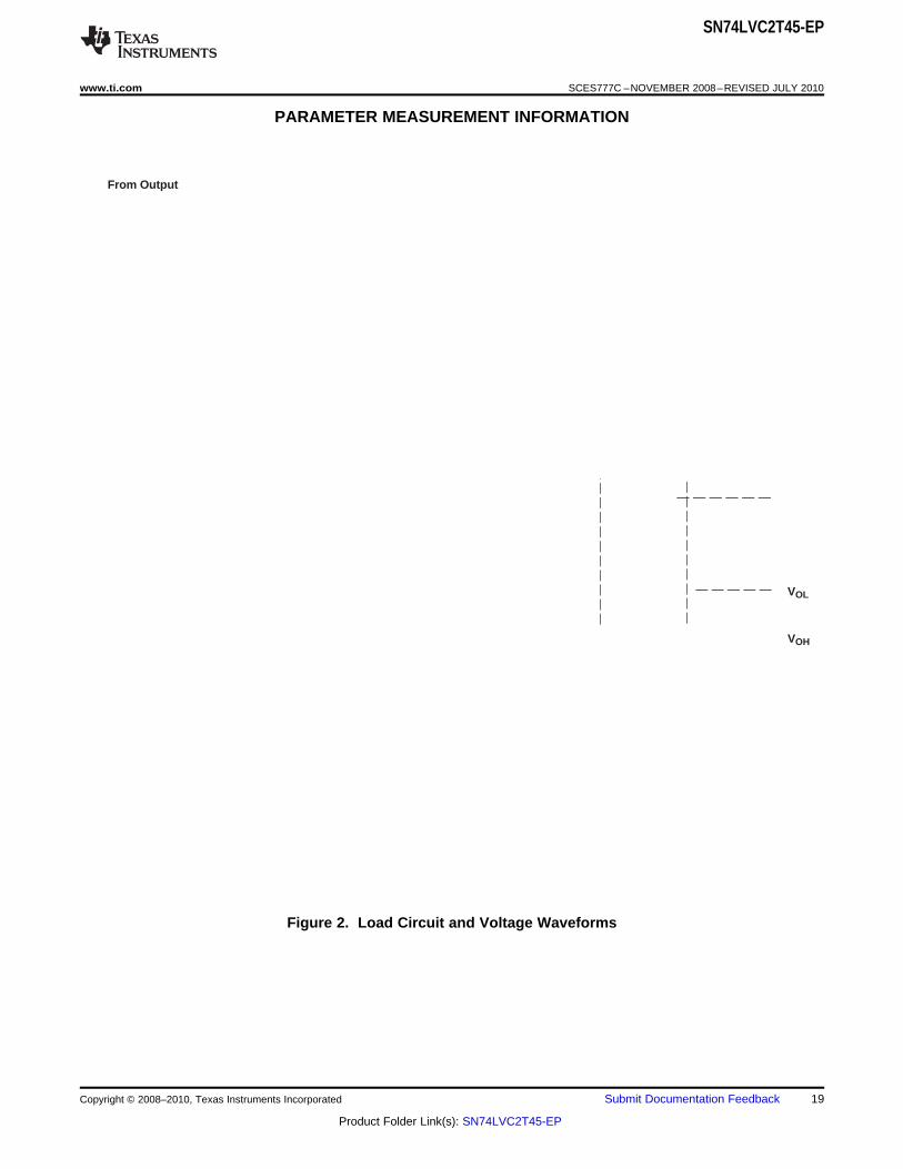
VOLTAGE WAVEFORMSPROPAGATION DELAY TIMES
VOLTAGE WAVEFORMSPULSE DURATION
VOLTAGE WAVEFORMSENABLE AND DISABLE TIMES
Output
Input
tpdtPLZ/tPZLtPHZ/tPZH
Open2 × VCCO
GND
TEST S1
NOTES: A. CL includes probe and jig capacitance.B. Waveform 1 is for an output with internal conditions such that the output is low, except when disabled by the output control.
Waveform 2 is for an output with internal conditions such that the output is high, except when disabled by the output control.C. All input pulses are supplied by generators having the following characteristics: PRR 10 MHz, ZO = 50 Ω, dv/dt ≥ 1 V/ns.D. The outputs are measured one at a time, with one transition per measurement.E. tPLZ and tPHZ are the same as tdis.F. tPZL and tPZH are the same as ten.G. tPLH and tPHL are the same as tpd.H. VCCI is the VCC associated with the input port.I. VCCO is the VCC associated with the output port.J. All parameters and waveforms are not applicable to all devices.
1.8 V ± 0.15 V2.5 V ± 0.2 V3.3 V ± 0.3 V5 V ± 0.5 V
2 kΩ2 kΩ2 kΩ2 kΩ
VCCO RL
0.15 V0.15 V0.3 V0.3 V
VTPCL
15 pF15 pF15 pF15 pF
SN74LVC2T45-EP
www.ti.com SCES777C –NOVEMBER 2008–REVISED JULY 2010
PARAMETER MEASUREMENT INFORMATION
Figure 2. Load Circuit and Voltage Waveforms
Copyright © 2008–2010, Texas Instruments Incorporated Submit Documentation Feedback 19
Product Folder Link(s): SN74LVC2T45-EP

VCC1
VCC1 VCC2
SYSTEM-1 SYSTEM-2
VCC1
1
2
3
4
8
7
6
5
VCC2
VCC2
SN74LVC2T45-EP
SCES777C –NOVEMBER 2008–REVISED JULY 2010 www.ti.com
APPLICATION INFORMATION
The following shows an example of the SN74LVC2T45 being used in a unidirectional logic level-shiftingapplication.
PIN NAME FUNCTION DESCRIPTION
1 VCCA VCC1 SYSTEM-1 supply voltage (1.65 V to 5.5 V)
2 A1 OUT1 Output level depends on VCC1 voltage.
3 A2 OUT2 Output level depends on VCC1 voltage.
4 GND GND Device GND
5 DIR DIR GND (low level) determines B-port to A-port direction.
6 B2 IN2 Input threshold value depends on VCC2 voltage.
7 B1 IN1 Input threshold value depends on VCC2 voltage.
8 VCCB VCC2 SYSTEM-2 supply voltage (1.65 V to 5.5 V)
Figure 3. Unidirectional Logic Level-Shifting Application
20 Submit Documentation Feedback Copyright © 2008–2010, Texas Instruments Incorporated
Product Folder Link(s): SN74LVC2T45-EP

VCC1 VCC1 VCC2
SYSTEM-1 SYSTEM-2
1
2
3
4
8
7
6
5
DIR CTRL
I/O-1Pullup/Down
or Bus Hold (1)
VCC2
I/O-2Pullup/Down
or Bus Hold (1)
SN74LVC2T45-EP
www.ti.com SCES777C –NOVEMBER 2008–REVISED JULY 2010
APPLICATION INFORMATION
Figure 4 shows the SN74LVC2T45 being used in a bidirectional logic level-shifting application. Since theSN74LVC2T45 does not have an output-enable (OE) pin, the system designer should take precautions to avoidbus contention between SYSTEM-1 and SYSTEM-2 when changing directions.
The following table shows data transmission from SYSTEM-1 to SYSTEM-2 and then from SYSTEM-2 toSYSTEM-1.
STATE DIR CTRL I/O-1 I/O-2 DESCRIPTION
1 H Out In SYSTEM-1 data to SYSTEM-2
SYSTEM-2 is getting ready to send data to SYSTEM-1. I/O-1 and I/O-2 are disabled. The2 H Hi-Z Hi-Z bus-line state depends on pullup or pulldown. (1)
DIR bit is flipped. I/O-1 and I/O-2 still are disabled. The bus-line state depends on pullup or3 L Hi-Z Hi-Z pulldown. (1)
4 L In Out SYSTEM-2 data to SYSTEM-1
(1) SYSTEM-1 and SYSTEM-2 must use the same conditions, i.e., both pullup or both pulldown.
Figure 4. Bidirectional Logic Level-Shifting Application
Enable Times
Calculate the enable times for the SN74LVC2T45 using the following formulas:• tPZH (DIR to A) = tPLZ (DIR to B) + tPLH (B to A)• tPZL (DIR to A) = tPHZ (DIR to B) + tPHL (B to A)• tPZH (DIR to B) = tPLZ (DIR to A) + tPLH (A to B)• tPZL (DIR to B) = tPHZ (DIR to A) + tPHL (A to B)
In a bidirectional application, these enable times provide the maximum delay from the time the DIR bit isswitched until an output is expected. For example, if the SN74LVC2T45 initially is transmitting from A to B, thenthe DIR bit is switched; the B port of the device must be disabled before presenting it with an input. After the Bport has been disabled, an input signal applied to it appears on the corresponding A port after the specifiedpropagation delay.
Copyright © 2008–2010, Texas Instruments Incorporated Submit Documentation Feedback 21
Product Folder Link(s): SN74LVC2T45-EP

PACKAGE OPTION ADDENDUM
www.ti.com 31-May-2014
Addendum-Page 1
PACKAGING INFORMATION
Orderable Device Status(1)
Package Type PackageDrawing
Pins PackageQty
Eco Plan(2)
Lead/Ball Finish(6)
MSL Peak Temp(3)
Op Temp (°C) Device Marking(4/5)
Samples
SN74LVC2T45MDCTTEP ACTIVE SM8 DCT 8 250 Green (RoHS& no Sb/Br)
CU NIPDAU Level-1-260C-UNLIM -55 to 125 NXRZ
V62/09604-01XE ACTIVE SM8 DCT 8 250 Green (RoHS& no Sb/Br)
CU NIPDAU Level-1-260C-UNLIM -55 to 125 NXRZ
(1) The marketing status values are defined as follows:ACTIVE: Product device recommended for new designs.LIFEBUY: TI has announced that the device will be discontinued, and a lifetime-buy period is in effect.NRND: Not recommended for new designs. Device is in production to support existing customers, but TI does not recommend using this part in a new design.PREVIEW: Device has been announced but is not in production. Samples may or may not be available.OBSOLETE: TI has discontinued the production of the device.
(2) Eco Plan - The planned eco-friendly classification: Pb-Free (RoHS), Pb-Free (RoHS Exempt), or Green (RoHS & no Sb/Br) - please check http://www.ti.com/productcontent for the latest availabilityinformation and additional product content details.TBD: The Pb-Free/Green conversion plan has not been defined.Pb-Free (RoHS): TI's terms "Lead-Free" or "Pb-Free" mean semiconductor products that are compatible with the current RoHS requirements for all 6 substances, including the requirement thatlead not exceed 0.1% by weight in homogeneous materials. Where designed to be soldered at high temperatures, TI Pb-Free products are suitable for use in specified lead-free processes.Pb-Free (RoHS Exempt): This component has a RoHS exemption for either 1) lead-based flip-chip solder bumps used between the die and package, or 2) lead-based die adhesive used betweenthe die and leadframe. The component is otherwise considered Pb-Free (RoHS compatible) as defined above.Green (RoHS & no Sb/Br): TI defines "Green" to mean Pb-Free (RoHS compatible), and free of Bromine (Br) and Antimony (Sb) based flame retardants (Br or Sb do not exceed 0.1% by weightin homogeneous material)
(3) MSL, Peak Temp. - The Moisture Sensitivity Level rating according to the JEDEC industry standard classifications, and peak solder temperature.
(4) There may be additional marking, which relates to the logo, the lot trace code information, or the environmental category on the device.
(5) Multiple Device Markings will be inside parentheses. Only one Device Marking contained in parentheses and separated by a "~" will appear on a device. If a line is indented then it is a continuationof the previous line and the two combined represent the entire Device Marking for that device.
(6) Lead/Ball Finish - Orderable Devices may have multiple material finish options. Finish options are separated by a vertical ruled line. Lead/Ball Finish values may wrap to two lines if the finishvalue exceeds the maximum column width.
Important Information and Disclaimer:The information provided on this page represents TI's knowledge and belief as of the date that it is provided. TI bases its knowledge and belief on informationprovided by third parties, and makes no representation or warranty as to the accuracy of such information. Efforts are underway to better integrate information from third parties. TI has taken andcontinues to take reasonable steps to provide representative and accurate information but may not have conducted destructive testing or chemical analysis on incoming materials and chemicals.TI and TI suppliers consider certain information to be proprietary, and thus CAS numbers and other limited information may not be available for release.

PACKAGE OPTION ADDENDUM
www.ti.com 31-May-2014
Addendum-Page 2
In no event shall TI's liability arising out of such information exceed the total purchase price of the TI part(s) at issue in this document sold by TI to Customer on an annual basis.
OTHER QUALIFIED VERSIONS OF SN74LVC2T45-EP :
• Catalog: SN74LVC2T45
• Automotive: SN74LVC2T45-Q1
NOTE: Qualified Version Definitions:
• Catalog - TI's standard catalog product
• Automotive - Q100 devices qualified for high-reliability automotive applications targeting zero defects
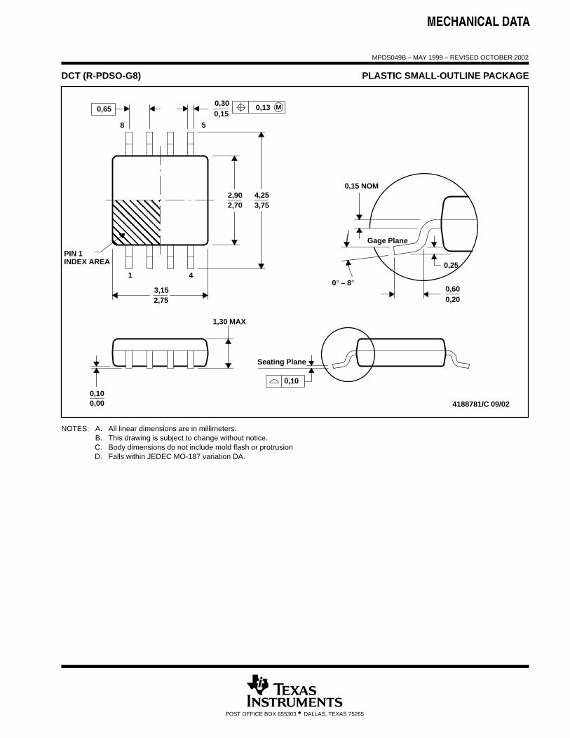
MECHANICAL DATA
MPDS049B – MAY 1999 – REVISED OCTOBER 2002
POST OFFICE BOX 655303 • DALLAS, TEXAS 75265
DCT (R-PDSO-G8) PLASTIC SMALL-OUTLINE PACKAGE
ÇÇÇÇÇÇÇÇÇÇÇÇÇÇÇÇÇÇÇÇ
0,600,20
0,25
0° – 8°
0,15 NOM
Gage Plane
4188781/C 09/02
4,25
5
0,300,15
2,903,752,70
8
4
3,152,75
1
0,100,00
1,30 MAX
Seating Plane
0,10
M0,130,65
PIN 1INDEX AREA
NOTES: A. All linear dimensions are in millimeters.B. This drawing is subject to change without notice.C. Body dimensions do not include mold flash or protrusionD. Falls within JEDEC MO-187 variation DA.

IMPORTANT NOTICETexas Instruments Incorporated and its subsidiaries (TI) reserve the right to make corrections, enhancements, improvements and otherchanges to its semiconductor products and services per JESD46, latest issue, and to discontinue any product or service per JESD48, latestissue. Buyers should obtain the latest relevant information before placing orders and should verify that such information is current andcomplete. All semiconductor products (also referred to herein as “components”) are sold subject to TI’s terms and conditions of salesupplied at the time of order acknowledgment.TI warrants performance of its components to the specifications applicable at the time of sale, in accordance with the warranty in TI’s termsand conditions of sale of semiconductor products. Testing and other quality control techniques are used to the extent TI deems necessaryto support this warranty. Except where mandated by applicable law, testing of all parameters of each component is not necessarilyperformed.TI assumes no liability for applications assistance or the design of Buyers’ products. Buyers are responsible for their products andapplications using TI components. To minimize the risks associated with Buyers’ products and applications, Buyers should provideadequate design and operating safeguards.TI does not warrant or represent that any license, either express or implied, is granted under any patent right, copyright, mask work right, orother intellectual property right relating to any combination, machine, or process in which TI components or services are used. Informationpublished by TI regarding third-party products or services does not constitute a license to use such products or services or a warranty orendorsement thereof. Use of such information may require a license from a third party under the patents or other intellectual property of thethird party, or a license from TI under the patents or other intellectual property of TI.Reproduction of significant portions of TI information in TI data books or data sheets is permissible only if reproduction is without alterationand is accompanied by all associated warranties, conditions, limitations, and notices. TI is not responsible or liable for such altereddocumentation. Information of third parties may be subject to additional restrictions.Resale of TI components or services with statements different from or beyond the parameters stated by TI for that component or servicevoids all express and any implied warranties for the associated TI component or service and is an unfair and deceptive business practice.TI is not responsible or liable for any such statements.Buyer acknowledges and agrees that it is solely responsible for compliance with all legal, regulatory and safety-related requirementsconcerning its products, and any use of TI components in its applications, notwithstanding any applications-related information or supportthat may be provided by TI. Buyer represents and agrees that it has all the necessary expertise to create and implement safeguards whichanticipate dangerous consequences of failures, monitor failures and their consequences, lessen the likelihood of failures that might causeharm and take appropriate remedial actions. Buyer will fully indemnify TI and its representatives against any damages arising out of the useof any TI components in safety-critical applications.In some cases, TI components may be promoted specifically to facilitate safety-related applications. With such components, TI’s goal is tohelp enable customers to design and create their own end-product solutions that meet applicable functional safety standards andrequirements. Nonetheless, such components are subject to these terms.No TI components are authorized for use in FDA Class III (or similar life-critical medical equipment) unless authorized officers of the partieshave executed a special agreement specifically governing such use.Only those TI components which TI has specifically designated as military grade or “enhanced plastic” are designed and intended for use inmilitary/aerospace applications or environments. Buyer acknowledges and agrees that any military or aerospace use of TI componentswhich have not been so designated is solely at the Buyer's risk, and that Buyer is solely responsible for compliance with all legal andregulatory requirements in connection with such use.TI has specifically designated certain components as meeting ISO/TS16949 requirements, mainly for automotive use. In any case of use ofnon-designated products, TI will not be responsible for any failure to meet ISO/TS16949.Products ApplicationsAudio www.ti.com/audio Automotive and Transportation www.ti.com/automotiveAmplifiers amplifier.ti.com Communications and Telecom www.ti.com/communicationsData Converters dataconverter.ti.com Computers and Peripherals www.ti.com/computersDLP® Products www.dlp.com Consumer Electronics www.ti.com/consumer-appsDSP dsp.ti.com Energy and Lighting www.ti.com/energyClocks and Timers www.ti.com/clocks Industrial www.ti.com/industrialInterface interface.ti.com Medical www.ti.com/medicalLogic logic.ti.com Security www.ti.com/securityPower Mgmt power.ti.com Space, Avionics and Defense www.ti.com/space-avionics-defenseMicrocontrollers microcontroller.ti.com Video and Imaging www.ti.com/videoRFID www.ti-rfid.comOMAP Applications Processors www.ti.com/omap TI E2E Community e2e.ti.comWireless Connectivity www.ti.com/wirelessconnectivity
Mailing Address: Texas Instruments, Post Office Box 655303, Dallas, Texas 75265Copyright © 2014, Texas Instruments Incorporated