Embed Size (px)
Citation preview
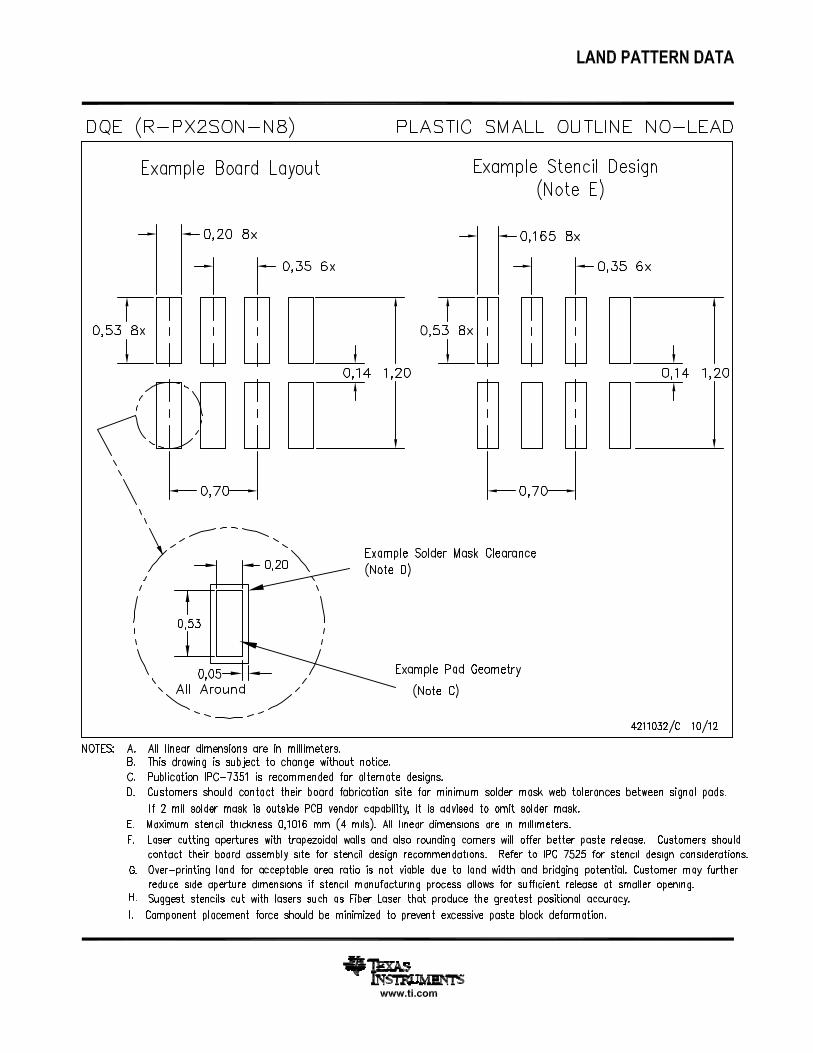
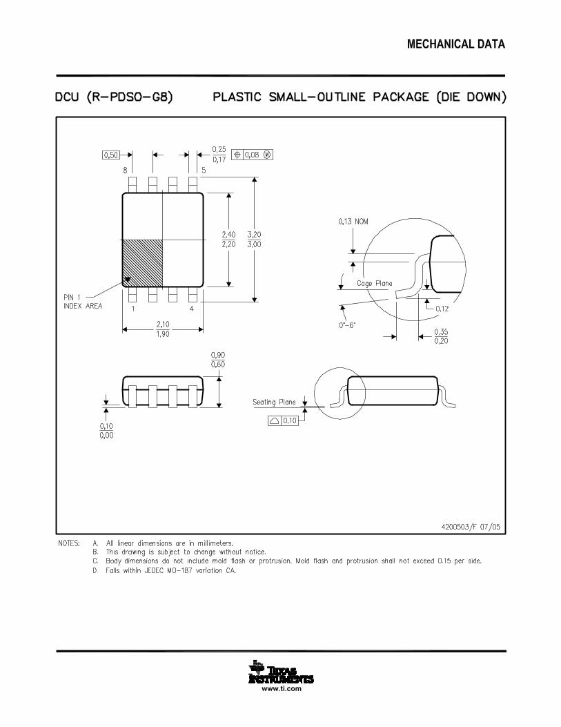
DCU PACKAGE
(TOP VIEW)
1 8
2 7
3 6
1A
1B
2Y
GND 4 5
VCC
1Y
2B
2A
RSE PACKAGE
(TOP VIEW)
1 7
2 6
8
3 54
VCC
1Y
2B
2A
GND
1A
1B
2Y
YFP OR YZP PACKAGE
(TOP VIEW)
1 8 VCC
2 7 1Y3 6 2B
1A
1B
2Y
GND 4 5 2A
1 8
2 7
3 6
1A
1B
2Y
GND 4 5
VCC
1Y
2B
2A
DQE PACKAGE
(TOP VIEW)
D1 D2
C1 C2
B1 B2
A1 A2
AUP
LVC
AUPAUP
LVC
Static-Power Consumption
(µA)
Dynamic-Power Consumption
(pF)
† Single, dual, and triple gates
3.3-VLogic †
3.3-VLogic †
0%
20%
40%
60%
80%
100%
0%
20%
40%
60%
80%
100%
−0.50
0.5
11.5
2
2.5
3
3.5
0 5 10 15 20 25 30 35 40 45Time − ns
Vol
tage
− V
† AUP1G08 data at CL = 15 pF
OutputInput
Switching Characteristics
at 25 MHz†
SN74AUP2G08
www.ti.com SCES681D –JANUARY 2008–REVISED OCTOBER 2010
LOW-POWER DUAL 2-INPUT POSITIVE-AND GATECheck for Samples: SN74AUP2G08
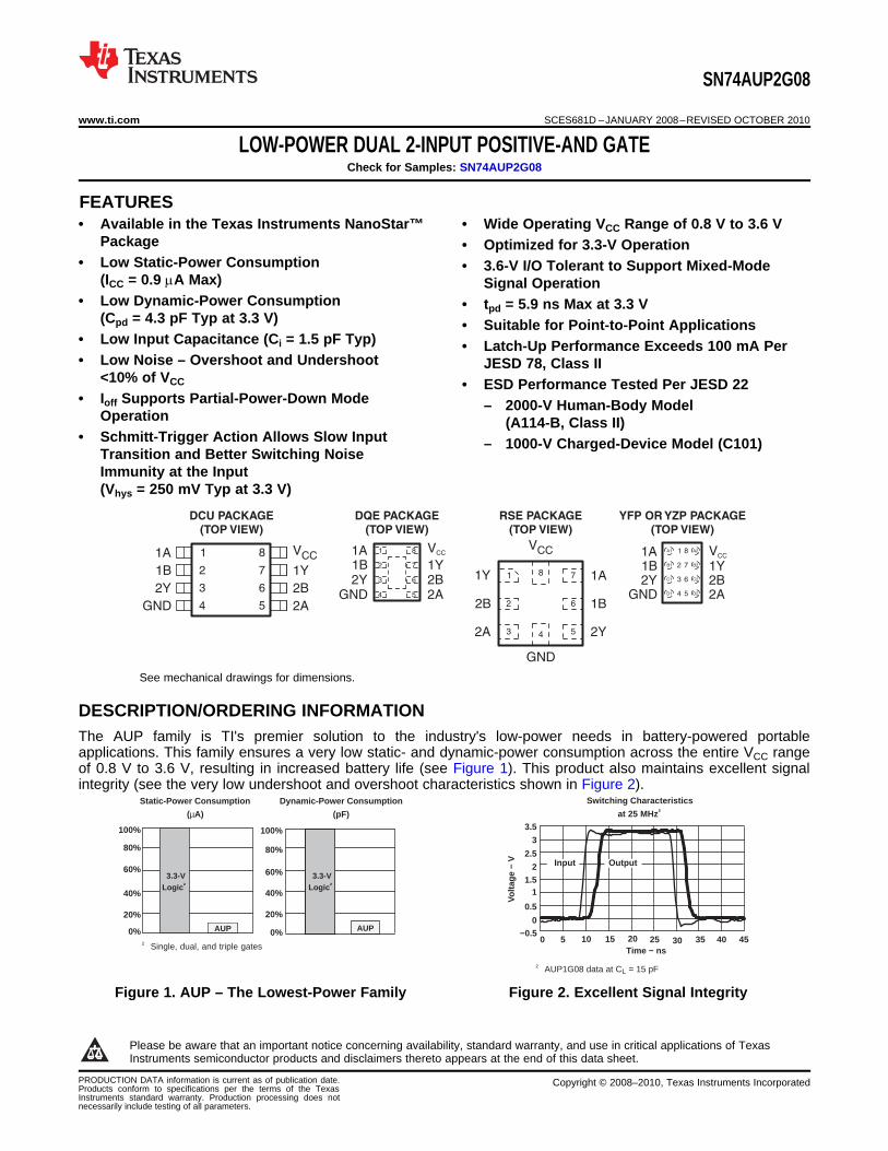
1FEATURES• Available in the Texas Instruments NanoStar™ • Wide Operating VCC Range of 0.8 V to 3.6 V
Package • Optimized for 3.3-V Operation• Low Static-Power Consumption • 3.6-V I/O Tolerant to Support Mixed-Mode
(ICC = 0.9 mA Max) Signal Operation• Low Dynamic-Power Consumption • tpd = 5.9 ns Max at 3.3 V
(Cpd = 4.3 pF Typ at 3.3 V) • Suitable for Point-to-Point Applications• Low Input Capacitance (Ci = 1.5 pF Typ) • Latch-Up Performance Exceeds 100 mA Per• Low Noise – Overshoot and Undershoot JESD 78, Class II
<10% of VCC • ESD Performance Tested Per JESD 22• Ioff Supports Partial-Power-Down Mode – 2000-V Human-Body Model
Operation (A114-B, Class II)• Schmitt-Trigger Action Allows Slow Input – 1000-V Charged-Device Model (C101)
Transition and Better Switching NoiseImmunity at the Input(Vhys = 250 mV Typ at 3.3 V)
See mechanical drawings for dimensions.
DESCRIPTION/ORDERING INFORMATIONThe AUP family is TI's premier solution to the industry's low-power needs in battery-powered portableapplications. This family ensures a very low static- and dynamic-power consumption across the entire VCC rangeof 0.8 V to 3.6 V, resulting in increased battery life (see Figure 1). This product also maintains excellent signalintegrity (see the very low undershoot and overshoot characteristics shown in Figure 2).
Figure 1. AUP – The Lowest-Power Family Figure 2. Excellent Signal Integrity
1
Please be aware that an important notice concerning availability, standard warranty, and use in critical applications of TexasInstruments semiconductor products and disclaimers thereto appears at the end of this data sheet.
PRODUCTION DATA information is current as of publication date. Copyright © 2008–2010, Texas Instruments IncorporatedProducts conform to specifications per the terms of the TexasInstruments standard warranty. Production processing does notnecessarily include testing of all parameters.

Y A • B or Y A B
1A1
27
1B1Y
2A5
63
2B2Y
SN74AUP2G08
SCES681D –JANUARY 2008–REVISED OCTOBER 2010 www.ti.com
This dual 2-input positive-AND gate performs the Boolean function in positive logic.
NanoStar™ package technology is a major breakthrough in IC packaging concepts, using the die as thepackage.
This device is fully specified for partial-power-down applications using Ioff. The Ioff circuitry disables the outputs,preventing damaging current backflow through the device when it is powered down.
ORDERING INFORMATION (1)
TA PACKAGE (2) ORDERABLE PART NUMBER TOP-SIDE MARKING (3)
NanoStar™ – WCSP (DSBGA) Reel of 3000 SN74AUP2G08YFPR _ _ _ HE_0.23-mm Large Bump – YFP
NanoStar™ – WCSP (DSBGA) Reel of 3000 SN74AUP2G08YZPR _ _ _ HE_0.23-mm Large Bump – YZP (Pb-free)–40°C to 85°CX2SON – DQE Reel of 5000 SN74AUP2G08DQER PR
QFN – RSE Reel of 5000 SN74AUP2G08RSER PR
VSSOP – DCU Reel of 3000 SN74AUP2G08DCUR H08_
(1) For the most current package and ordering information, see the Package Option Addendum at the end of this document, or see the TIweb site at www.ti.com.
(2) Package drawings, thermal data, and symbolization are available at www.ti.com/packaging.(3) YFP/YZP: The actual top-side marking has three preceding characters to denote year, month, and sequence code, and one following
character to designate the wafer fab/assembly site. Pin 1 identifier indicates solder-bump composition (1 = SnPb, • = Pb-free).DCU: The actual top-side marking has one additional character to denote wafer fab/assembly site.
FUNCTION TABLEINPUTS OUTPUT
YA B
L L L
L H L
H L L
H H H
LOGIC DIAGRAM (POSITIVE LOGIC)
Pin numbers shown are for DCU, YFP, and YZP packages.
2 Submit Documentation Feedback Copyright © 2008–2010, Texas Instruments Incorporated
Product Folder Link(s): SN74AUP2G08

SN74AUP2G08
www.ti.com SCES681D –JANUARY 2008–REVISED OCTOBER 2010
ABSOLUTE MAXIMUM RATINGS (1)
over operating free-air temperature range (unless otherwise noted)MIN MAX UNIT
VCC Supply voltage range –0.5 4.6 V
VI Input voltage range (2) –0.5 4.6 V
VO Voltage range applied to any output in the high-impedance or power-off state (2) –0.5 4.6 V
VO Output voltage range in the high or low state (2) –0.5 VCC + 0.5 V
IIK Input clamp current VI < 0 –50 mA
IOK Output clamp current VO < 0 –50 mA
IO Continuous output current ±20 mA
Continuous current through VCC or GND ±50 mA
DCU package 227
DQE package 261
qJA Package thermal impedance (3) RSE package 253 °C/W
YFP package 98.8
YZP package 102
Tstg Storage temperature range –65 150 °C
(1) Stresses beyond those listed under "absolute maximum ratings" may cause permanent damage to the device. These are stress ratingsonly, and functional operation of the device at these or any other conditions beyond those indicated under "recommended operatingconditions" is not implied. Exposure to absolute-maximum-rated conditions for extended periods may affect device reliability.
(2) The input negative-voltage and output voltage ratings may be exceeded if the input and output current ratings are observed.(3) The package thermal impedance is calculated in accordance with JESD 51-7.
Copyright © 2008–2010, Texas Instruments Incorporated Submit Documentation Feedback 3
Product Folder Link(s): SN74AUP2G08

SN74AUP2G08
SCES681D –JANUARY 2008–REVISED OCTOBER 2010 www.ti.com
RECOMMENDED OPERATING CONDITIONS (1)
MIN MAX UNIT
VCC Supply voltage 0.8 3.6 V
VCC = 0.8 V VCC
VCC = 1.1 V to 1.95 V 0.65 × VCCVIH High-level input voltage V
VCC = 2.3 V to 2.7 V 1.6
VCC = 3 V to 3.6 V 2
VCC = 0.8 V 0
VCC = 1.1 V to 1.95 V 0.35 × VCCVIL Low-level input voltage V
VCC = 2.3 V to 2.7 V 0.7
VCC = 3 V to 3.6 V 0.9
VI Input voltage 0 3.6 V
VO Output voltage 0 VCC V
VCC = 0.8 V –20 mA
VCC = 1.1 V –1.1
VCC = 1.4 V –1.7IOH High-level output current
VCC = 1.65 –1.9 mA
VCC = 2.3 V –3.1
VCC = 3 V –4
VCC = 0.8 V 20 mA
VCC = 1.1 V 1.1
VCC = 1.4 V 1.7IOL Low-level output current
VCC = 1.65 V 1.9 mA
VCC = 2.3 V 3.1
VCC = 3 V 4
Δt/Δv Input transition rise or fall rate VCC = 0.8 V to 3.6 V 200 ns/V
TA Operating free-air temperature –40 85 °C
(1) All unused inputs of the device must be held at VCC or GND to ensure proper device operation. See the TI application report,Implications of Slow or Floating CMOS Inputs, literature number SCBA004.
4 Submit Documentation Feedback Copyright © 2008–2010, Texas Instruments Incorporated
Product Folder Link(s): SN74AUP2G08

SN74AUP2G08
www.ti.com SCES681D –JANUARY 2008–REVISED OCTOBER 2010
ELECTRICAL CHARACTERISTICSover recommended operating free-air temperature range (unless otherwise noted)
TA = 25°C TA = –40°C to 85°CPARAMETER TEST CONDITIONS VCC UNIT
MIN TYP MAX MIN MAX
IOH = –20 mA 0.8 V to 3.6 V VCC – 0.1 VCC – 0.1
IOH = –1.1 mA 1.1 V 0.75 × VCC 0.7 × VCC
IOH = –1.7 mA 1.4 V 1.11 1.03
IOH = –1.9 mA 1.65 V 1.32 1.3VOH V
IOH = –2.3 mA 2.05 1.972.3 V
IOH = –3.1 mA 1.9 1.85
IOH = –2.7 mA 2.72 2.673 V
IOH = –4 mA 2.6 2.55
IOL = 20 mA 0.8 V to 3.6 V 0.1 0.1
IOL = 1.1 mA 1.1 V 0.3 × VCC 0.3 × VCC
IOL = 1.7 mA 1.4 V 0.31 0.37
IOL = 1.9 mA 1.65 V 0.31 0.35VOL V
IOL = 2.3 mA 0.31 0.332.3 V
IOL = 3.1 mA 0.44 0.45
IOL = 2.7 mA 0.31 0.333 V
IOL = 4 mA 0.44 0.45
II A or B input VI = GND to 3.6 V 0 V to 3.6 V 0.1 0.5 mA
Ioff VI or VO = 0 V to 3.6 V 0 V 0.2 0.6 mA
ΔIoff VI or VO = 0 V to 3.6 V 0 V to 0.2 V 0.2 0.9 mA
VI = GND or IO = 0ICC 0.8 V to 3.6 V 0.5 0.9 mA(VCC to 3.6 V)
ΔICC VI = VCC – 0.6 V (1), IO = 0 3.3 V 40 50 mA
0 V 2Ci VI = VCC or GND pF
3.6 V 2
Co VO = GND 0 V 3 pF
(1) One input at VCC – 0.6 V, other input at VCC or GND
Copyright © 2008–2010, Texas Instruments Incorporated Submit Documentation Feedback 5
Product Folder Link(s): SN74AUP2G08

SN74AUP2G08
SCES681D –JANUARY 2008–REVISED OCTOBER 2010 www.ti.com
SWITCHING CHARACTERISTICSover recommended operating free-air temperature range, CL = 5 pF (unless otherwise noted) (see Figure 3 and Figure 4)
TA = 25°C TA = –40°C to 85°CFROM TOPARAMETER VCC UNIT(INPUT) (OUTPUT) MIN TYP MAX MIN MAX
0.8 V 19.8
1.2 V ± 0.1 V 0.5 7.8 18.8 0.5 19.8
1.5 V ± 0.1 V 0.5 5.4 11.8 0.5 13.9tpd A or B Y ns
1.8 V ± 0.15 V 0.5 4.3 9 0.5 11.1
2.5 V ± 0.2 V 0.5 3 5.7 0.5 7.8
3.3 V ± 0.3 V 0.5 2.4 4.6 0.5 5.9
SWITCHING CHARACTERISTICSover recommended operating free-air temperature range, CL = 10 pF (unless otherwise noted) (see Figure 3 and Figure 4)
TA = 25°C TA = –40°C to 85°CFROM TOPARAMETER VCC UNIT(INPUT) (OUTPUT) MIN TYP MAX MIN MAX
0.8 V 23.1
1.2 V ± 0.1 V 0.5 8.9 21.1 0.5 22
1.5 V ± 0.1 V 0.8 6.3 13.2 0.5 15.1tpd A or B Y ns
1.8 V ± 0.15 V 0.6 5 10.1 0.5 12.2
2.5 V ± 0.2 V 0.5 3.6 7.4 0.5 9
3.3 V ± 0.3 V 0.5 2.9 5.1 0.5 6.5
6 Submit Documentation Feedback Copyright © 2008–2010, Texas Instruments Incorporated
Product Folder Link(s): SN74AUP2G08

SN74AUP2G08
www.ti.com SCES681D –JANUARY 2008–REVISED OCTOBER 2010
SWITCHING CHARACTERISTICSover recommended operating free-air temperature range, CL = 15 pF (unless otherwise noted) (see Figure 3 and Figure 4)
TA = 25°C TA = –40°C to 85°CFROM TOPARAMETER VCC UNIT(INPUT) (OUTPUT) MIN TYP MAX MIN MAX
0.8 V 24.7
1.2 V ± 0.1 V 0.5 9.8 21.7 0.5 22.7
1.5 V ± 0.1 V 1.3 4.6 14 0.5 15.7tpd A or B Y ns
1.8 V ± 0.15 V 1.2 5.5 10.6 0.5 12.6
2.5 V ± 0.2 V 0.7 4 7 0.5 8.9
3.3 V ± 0.3 V 0.9 3.3 5.5 0.5 6.9
SWITCHING CHARACTERISTICSover recommended operating free-air temperature range, CL = 30 pF (unless otherwise noted) (see Figure 3 and Figure 4)
TA = 25°C TA = –40°C to 85°CFROM TOPARAMETER VCC UNIT(INPUT) (OUTPUT) MIN TYP MAX MIN MAX
0.8 V 31.8
1.2 V ± 0.1 V 0.6 12.6 26.3 0.5 27
1.5 V ± 0.1 V 2.5 9 16.6 0.7 18.3tpd A or B Y ns
1.8 V ± 0.15 V 2.3 7.3 12.9 0.5 14.8
2.5 V ± 0.2 V 2.1 5.4 8.8 0.8 10.5
3.3 V ± 0.3 V 2.1 4.5 6.7 0.9 8.2
OPERATING CHARACTERISTICSTA = 25°C
PARAMETER TEST CONDITIONS VCC TYP UNIT
0.8 V 4
1.2 V ± 0.1 V 4
1.5 V ± 0.1 V 4Cpd Power dissipation capacitance f = 10 MHz pF
1.8 V ± 0.15 V 4
2.5 V ± 0.2 V 4.1
3.3 V ± 0.3 V 4.3
Copyright © 2008–2010, Texas Instruments Incorporated Submit Documentation Feedback 7
Product Folder Link(s): SN74AUP2G08
VM
From OutputUnder Test
CL(see Note A)
LOAD CIRCUIT
1 MΩ
VOLTAGE WAVEFORMSPROPAGATION DELAY TIMES
INVERTING AND NONINVERTING OUTPUTS
tPLH
tPHL
tPHL
tPLH
VOH
VOH
VOL
VOL
VI
0 VInput
Output
Output
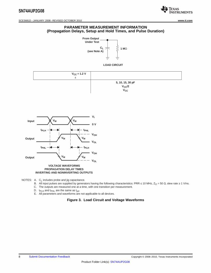
NOTES: A. CL includes probe and jig capacitance.B. All input pulses are supplied by generators having the following characteristics: PRR ≤ 10 MHz, ZO = 50 Ω, slew rate ≥ 1 V/ns.C. The outputs are measured one at a time, with one transition per measurement.D. tPLH and tPHL are the same as tpd.E. All parameters and waveforms are not applicable to all devices.
VM VM
VM VM
VM
5, 10, 15, 30 pFVCC/2VCC
VCC = 1.2 V± 0.1 V
VCC = 0.8 VVCC = 1.5 V
± 0.1 VVCC = 1.8 V
± 0.15 VVCC = 2.5 V
± 0.2 VVCC = 3.3 V
± 0.3 V
5, 10, 15, 30 pFVCC/2VCC
5, 10, 15, 30 pFVCC/2VCC
5, 10, 15, 30 pFVCC/2VCC
CLVMVI
5, 10, 15, 30 pFVCC/2VCC
5, 10, 15, 30 pFVCC/2VCC
thtsu
Data Input
Timing InputVCC
0 V
VCC
0 V
0 V
tw
Input
VOLTAGE WAVEFORMSSETUP AND HOLD TIMES
VOLTAGE WAVEFORMSPULSE DURATION
VCC/2 VCC/2
VCC/2
VCC/2
VCC
VCC/2
SN74AUP2G08
SCES681D –JANUARY 2008–REVISED OCTOBER 2010 www.ti.com
PARAMETER MEASUREMENT INFORMATION(Propagation Delays, Setup and Hold Times, and Pulse Duration)
Figure 3. Load Circuit and Voltage Waveforms
8 Submit Documentation Feedback Copyright © 2008–2010, Texas Instruments Incorporated
Product Folder Link(s): SN74AUP2G08

NOTES: A. CL includes probe and jig capacitance.B. Waveform 1 is for an output with internal conditions such that the output is low, except when disabled by the output control.
Waveform 2 is for an output with internal conditions such that the output is high, except when disabled by the output control.C. All input pulses are supplied by generators having the following characteristics: PRR ≤ 10 MHz, ZO = 50 Ω, slew rate ≥ 1 V/ns.D. The outputs are measured one at a time, with one transition per measurement.E. tPLZ and tPHZ are the same as tdis.F. tPZL and tPZH are the same as ten.G. All parameters and waveforms are not applicable to all devices.
5, 10, 15, 30 pFVCC/2VCC
0.15 V
VCC = 1.2 V± 0.1 V
VCC = 0.8 VVCC = 1.5 V
± 0.1 VVCC = 1.8 V
± 0.15 VVCC = 2.5 V
± 0.2 VVCC = 3.3 V
± 0.3 V
5, 10, 15, 30 pFVCC/2VCC0.1 V
5, 10, 15, 30 pFVCC/2VCC0.1 V
5, 10, 15, 30 pFVCC/2VCC0.1 V
CLVMVIV∆
5, 10, 15, 30 pFVCC/2VCC
0.15 V
5, 10, 15, 30 pFVCC/2VCC0.3 V
OutputWaveform 1
S1 at 2 × VCC(see Note B)
OutputWaveform 2
S1 at GND(see Note B)
VOL
VOH
tPZL
tPZH
tPLZ
tPHZ
VCC
0 V
VOL + V∆
VOH - V∆
≈0 V
VCC
VOLTAGE WAVEFORMSENABLE AND DISABLE TIMES
LOW- AND HIGH-LEVEL ENABLING
OutputControl
VCC/2 VCC/2
VCC/2
VCC/2
tPLZ/tPZLtPHZ/tPZH
2 × VCCGND
TEST S1From Output
Under Test
CL(see Note A)
LOAD CIRCUIT
S1
GND
5 kΩ
5 kΩ
2 × VCC
SN74AUP2G08
www.ti.com SCES681D –JANUARY 2008–REVISED OCTOBER 2010
PARAMETER MEASUREMENT INFORMATION(Enable and Disable Times)
Figure 4. Load Circuit and Voltage Waveforms
Copyright © 2008–2010, Texas Instruments Incorporated Submit Documentation Feedback 9
Product Folder Link(s): SN74AUP2G08

PACKAGE OPTION ADDENDUM
www.ti.com 24-Mar-2017
Addendum-Page 1
PACKAGING INFORMATION
Orderable Device Status(1)
Package Type PackageDrawing
Pins PackageQty
Eco Plan(2)
Lead/Ball Finish(6)
MSL Peak Temp(3)
Op Temp (°C) Device Marking(4/5)
Samples
SN74AUP2G08DCUR ACTIVE VSSOP DCU 8 3000 Green (RoHS& no Sb/Br)
CU NIPDAU Level-1-260C-UNLIM -40 to 85 H08R
SN74AUP2G08DQER ACTIVE X2SON DQE 8 5000 Green (RoHS& no Sb/Br)
CU NIPDAUAG Level-1-260C-UNLIM -40 to 85 PR
SN74AUP2G08RSER ACTIVE UQFN RSE 8 5000 Green (RoHS& no Sb/Br)
CU NIPDAUAG Level-1-260C-UNLIM -40 to 85 PR
SN74AUP2G08YFPR ACTIVE DSBGA YFP 8 3000 Green (RoHS& no Sb/Br)
SNAGCU Level-1-260C-UNLIM -40 to 85 HEN
SN74AUP2G08YZPR ACTIVE DSBGA YZP 8 3000 Green (RoHS& no Sb/Br)
SNAGCU Level-1-260C-UNLIM -40 to 85 HEN
(1) The marketing status values are defined as follows:ACTIVE: Product device recommended for new designs.LIFEBUY: TI has announced that the device will be discontinued, and a lifetime-buy period is in effect.NRND: Not recommended for new designs. Device is in production to support existing customers, but TI does not recommend using this part in a new design.PREVIEW: Device has been announced but is not in production. Samples may or may not be available.OBSOLETE: TI has discontinued the production of the device.
(2) Eco Plan - The planned eco-friendly classification: Pb-Free (RoHS), Pb-Free (RoHS Exempt), or Green (RoHS & no Sb/Br) - please check http://www.ti.com/productcontent for the latest availabilityinformation and additional product content details.TBD: The Pb-Free/Green conversion plan has not been defined.Pb-Free (RoHS): TI's terms "Lead-Free" or "Pb-Free" mean semiconductor products that are compatible with the current RoHS requirements for all 6 substances, including the requirement thatlead not exceed 0.1% by weight in homogeneous materials. Where designed to be soldered at high temperatures, TI Pb-Free products are suitable for use in specified lead-free processes.Pb-Free (RoHS Exempt): This component has a RoHS exemption for either 1) lead-based flip-chip solder bumps used between the die and package, or 2) lead-based die adhesive used betweenthe die and leadframe. The component is otherwise considered Pb-Free (RoHS compatible) as defined above.Green (RoHS & no Sb/Br): TI defines "Green" to mean Pb-Free (RoHS compatible), and free of Bromine (Br) and Antimony (Sb) based flame retardants (Br or Sb do not exceed 0.1% by weightin homogeneous material)
(3) MSL, Peak Temp. - The Moisture Sensitivity Level rating according to the JEDEC industry standard classifications, and peak solder temperature.
(4) There may be additional marking, which relates to the logo, the lot trace code information, or the environmental category on the device.
(5) Multiple Device Markings will be inside parentheses. Only one Device Marking contained in parentheses and separated by a "~" will appear on a device. If a line is indented then it is a continuationof the previous line and the two combined represent the entire Device Marking for that device.
PACKAGE OPTION ADDENDUM
www.ti.com 24-Mar-2017
Addendum-Page 2
(6) Lead/Ball Finish - Orderable Devices may have multiple material finish options. Finish options are separated by a vertical ruled line. Lead/Ball Finish values may wrap to two lines if the finishvalue exceeds the maximum column width.
Important Information and Disclaimer:The information provided on this page represents TI's knowledge and belief as of the date that it is provided. TI bases its knowledge and belief on informationprovided by third parties, and makes no representation or warranty as to the accuracy of such information. Efforts are underway to better integrate information from third parties. TI has taken andcontinues to take reasonable steps to provide representative and accurate information but may not have conducted destructive testing or chemical analysis on incoming materials and chemicals.TI and TI suppliers consider certain information to be proprietary, and thus CAS numbers and other limited information may not be available for release.
In no event shall TI's liability arising out of such information exceed the total purchase price of the TI part(s) at issue in this document sold by TI to Customer on an annual basis.
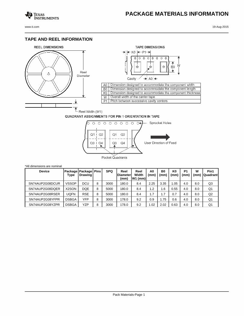
TAPE AND REEL INFORMATION
*All dimensions are nominal
Device PackageType
PackageDrawing
Pins SPQ ReelDiameter
(mm)
ReelWidth
W1 (mm)
A0(mm)
B0(mm)
K0(mm)
P1(mm)
W(mm)
Pin1Quadrant
SN74AUP2G08DCUR VSSOP DCU 8 3000 180.0 8.4 2.25 3.35 1.05 4.0 8.0 Q3
SN74AUP2G08DQER X2SON DQE 8 5000 180.0 8.4 1.2 1.6 0.55 4.0 8.0 Q1
SN74AUP2G08RSER UQFN RSE 8 5000 180.0 8.4 1.7 1.7 0.7 4.0 8.0 Q2
SN74AUP2G08YFPR DSBGA YFP 8 3000 178.0 9.2 0.9 1.75 0.6 4.0 8.0 Q1
SN74AUP2G08YZPR DSBGA YZP 8 3000 178.0 9.2 1.02 2.02 0.63 4.0 8.0 Q1
PACKAGE MATERIALS INFORMATION
www.ti.com 19-Aug-2015
Pack Materials-Page 1
*All dimensions are nominal
Device Package Type Package Drawing Pins SPQ Length (mm) Width (mm) Height (mm)
SN74AUP2G08DCUR VSSOP DCU 8 3000 202.0 201.0 28.0
SN74AUP2G08DQER X2SON DQE 8 5000 202.0 201.0 28.0
SN74AUP2G08RSER UQFN RSE 8 5000 202.0 201.0 28.0
SN74AUP2G08YFPR DSBGA YFP 8 3000 220.0 220.0 35.0
SN74AUP2G08YZPR DSBGA YZP 8 3000 220.0 220.0 35.0
PACKAGE MATERIALS INFORMATION
www.ti.com 19-Aug-2015
Pack Materials-Page 2
www.ti.com
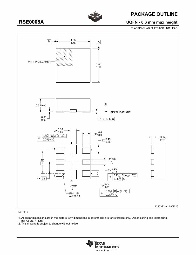
PACKAGE OUTLINE
C0.6 MAX
0.050.00
2X1
4X 0.5
6X 0.40.3
4X 0.30.2
2X 0.450.35
2X 0.250.15
2X 0.350.25
B 1.551.45 A
1.551.45
(0.12)TYP
UQFN - 0.6 mm max heightRSE0008APLASTIC QUAD FLATPACK - NO LEAD
4220323/A 03/2016
PIN 1 INDEX AREA
SEATING PLANE
0.05 C
1
3
4
8
0.1 C A B0.05 C
5
7
SYMM
SYMM
0.1 C A B0.05 C
PIN 1 ID(45 X 0.1
NOTES: 1. All linear dimensions are in millimeters. Any dimensions in parenthesis are for reference only. Dimensioning and tolerancing per ASME Y14.5M. 2. This drawing is subject to change without notice.
0.1 C A B0.05 C
SCALE 7.000

www.ti.com
EXAMPLE BOARD LAYOUT
2X (0.6)
2X (0.3)
2X(0.2)
0.07 MINALL AROUND
0.07 MAXALL AROUND
6X (0.55)
4X (0.25)
4X (0.5)
(1.35)
(1.3)
(R ) TYP0.05
UQFN - 0.6 mm max heightRSE0008APLASTIC QUAD FLATPACK - NO LEAD
4220323/A 03/2016
SYMM
1
35
8
SYMM
LAND PATTERN EXAMPLESCALE:30X
4
7
NOTES: (continued) 3. For more information, see Texas Instruments literature number SLUA271 (www.ti.com/lit/slua271).
METAL
SOLDER MASKOPENING
SOLDER MASK DETAILSNOT TO SCALE
NON SOLDER MASKDEFINED
(PREFERRED)
SOLDER MASKOPENING
METALUNDERSOLDER MASK
SOLDER MASKDEFINED
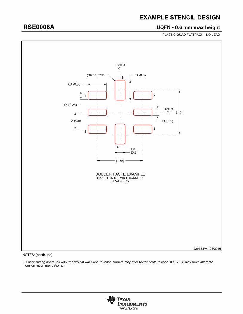
www.ti.com
EXAMPLE STENCIL DESIGN
6X (0.55)
4X (0.25)
2X (0.6)
2X(0.3)
(1.35)
(1.3)
2X (0.2)4X (0.5)
(R ) TYP0.05
UQFN - 0.6 mm max heightRSE0008APLASTIC QUAD FLATPACK - NO LEAD
4220323/A 03/2016
NOTES: (continued) 5. Laser cutting apertures with trapezoidal walls and rounded corners may offer better paste release. IPC-7525 may have alternate design recommendations.
SYMM
1
3
4
5
7
8
SYMM
SOLDER PASTE EXAMPLEBASED ON 0.1 mm THICKNESS
SCALE: 30X


www.ti.com
PACKAGE OUTLINE
C0.5 MAX
0.190.15
1.5TYP
0.5 TYP
8X 0.250.21
0.5TYP
B E A
D
4223082/A 07/2016
DSBGA - 0.5 mm max heightYZP0008DIE SIZE BALL GRID ARRAY
NOTES: 1. All linear dimensions are in millimeters. Any dimensions in parenthesis are for reference only. Dimensioning and tolerancing per ASME Y14.5M.2. This drawing is subject to change without notice.
BALL A1CORNER
SEATING PLANE
BALL TYP0.05 C
B
1 2
0.015 C A B
SYMM
SYMM
C
A
D
SCALE 8.000
D: Max =
E: Max =
1.918 mm, Min =
0.918 mm, Min =
1.858 mm
0.858 mm

www.ti.com
EXAMPLE BOARD LAYOUT
8X ( 0.23)(0.5) TYP
(0.5) TYP
( 0.23)METAL
0.05 MAX ( 0.23)SOLDER MASKOPENING
0.05 MIN
4223082/A 07/2016
DSBGA - 0.5 mm max heightYZP0008DIE SIZE BALL GRID ARRAY
NOTES: (continued) 3. Final dimensions may vary due to manufacturing tolerance considerations and also routing constraints. For more information, see Texas Instruments literature number SNVA009 (www.ti.com/lit/snva009).
SYMM
SYMM
LAND PATTERN EXAMPLESCALE:40X
1 2
A
B
C
D
NON-SOLDER MASKDEFINED
(PREFERRED)
SOLDER MASK DETAILSNOT TO SCALE
SOLDER MASKOPENING
SOLDER MASKDEFINED
METAL UNDERSOLDER MASK

www.ti.com
EXAMPLE STENCIL DESIGN
(0.5)TYP
(0.5) TYP
8X ( 0.25) (R0.05) TYP
METALTYP
4223082/A 07/2016
DSBGA - 0.5 mm max heightYZP0008DIE SIZE BALL GRID ARRAY
NOTES: (continued) 4. Laser cutting apertures with trapezoidal walls and rounded corners may offer better paste release.
SYMM
SYMM
SOLDER PASTE EXAMPLEBASED ON 0.1 mm THICK STENCIL
SCALE:40X
1 2
A
B
C
D

D: Max =
E: Max =
1.59 mm, Min =
0.79 mm, Min =
1.53 mm
0.73 mm

IMPORTANT NOTICE FOR TI DESIGN INFORMATION AND RESOURCES
Texas Instruments Incorporated (‘TI”) technical, application or other design advice, services or information, including, but not limited to,reference designs and materials relating to evaluation modules, (collectively, “TI Resources”) are intended to assist designers who aredeveloping applications that incorporate TI products; by downloading, accessing or using any particular TI Resource in any way, you(individually or, if you are acting on behalf of a company, your company) agree to use it solely for this purpose and subject to the terms ofthis Notice.TI’s provision of TI Resources does not expand or otherwise alter TI’s applicable published warranties or warranty disclaimers for TIproducts, and no additional obligations or liabilities arise from TI providing such TI Resources. TI reserves the right to make corrections,enhancements, improvements and other changes to its TI Resources.You understand and agree that you remain responsible for using your independent analysis, evaluation and judgment in designing yourapplications and that you have full and exclusive responsibility to assure the safety of your applications and compliance of your applications(and of all TI products used in or for your applications) with all applicable regulations, laws and other applicable requirements. Yourepresent that, with respect to your applications, you have all the necessary expertise to create and implement safeguards that (1)anticipate dangerous consequences of failures, (2) monitor failures and their consequences, and (3) lessen the likelihood of failures thatmight cause harm and take appropriate actions. You agree that prior to using or distributing any applications that include TI products, youwill thoroughly test such applications and the functionality of such TI products as used in such applications. TI has not conducted anytesting other than that specifically described in the published documentation for a particular TI Resource.You are authorized to use, copy and modify any individual TI Resource only in connection with the development of applications that includethe TI product(s) identified in such TI Resource. NO OTHER LICENSE, EXPRESS OR IMPLIED, BY ESTOPPEL OR OTHERWISE TOANY OTHER TI INTELLECTUAL PROPERTY RIGHT, AND NO LICENSE TO ANY TECHNOLOGY OR INTELLECTUAL PROPERTYRIGHT OF TI OR ANY THIRD PARTY IS GRANTED HEREIN, including but not limited to any patent right, copyright, mask work right, orother intellectual property right relating to any combination, machine, or process in which TI products or services are used. Informationregarding or referencing third-party products or services does not constitute a license to use such products or services, or a warranty orendorsement thereof. Use of TI Resources may require a license from a third party under the patents or other intellectual property of thethird party, or a license from TI under the patents or other intellectual property of TI.TI RESOURCES ARE PROVIDED “AS IS” AND WITH ALL FAULTS. TI DISCLAIMS ALL OTHER WARRANTIES ORREPRESENTATIONS, EXPRESS OR IMPLIED, REGARDING TI RESOURCES OR USE THEREOF, INCLUDING BUT NOT LIMITED TOACCURACY OR COMPLETENESS, TITLE, ANY EPIDEMIC FAILURE WARRANTY AND ANY IMPLIED WARRANTIES OFMERCHANTABILITY, FITNESS FOR A PARTICULAR PURPOSE, AND NON-INFRINGEMENT OF ANY THIRD PARTY INTELLECTUALPROPERTY RIGHTS.TI SHALL NOT BE LIABLE FOR AND SHALL NOT DEFEND OR INDEMNIFY YOU AGAINST ANY CLAIM, INCLUDING BUT NOTLIMITED TO ANY INFRINGEMENT CLAIM THAT RELATES TO OR IS BASED ON ANY COMBINATION OF PRODUCTS EVEN IFDESCRIBED IN TI RESOURCES OR OTHERWISE. IN NO EVENT SHALL TI BE LIABLE FOR ANY ACTUAL, DIRECT, SPECIAL,COLLATERAL, INDIRECT, PUNITIVE, INCIDENTAL, CONSEQUENTIAL OR EXEMPLARY DAMAGES IN CONNECTION WITH ORARISING OUT OF TI RESOURCES OR USE THEREOF, AND REGARDLESS OF WHETHER TI HAS BEEN ADVISED OF THEPOSSIBILITY OF SUCH DAMAGES.You agree to fully indemnify TI and its representatives against any damages, costs, losses, and/or liabilities arising out of your non-compliance with the terms and provisions of this Notice.This Notice applies to TI Resources. Additional terms apply to the use and purchase of certain types of materials, TI products and services.These include; without limitation, TI’s standard terms for semiconductor products http://www.ti.com/sc/docs/stdterms.htm), evaluationmodules, and samples (http://www.ti.com/sc/docs/sampterms.htm).
Mailing Address: Texas Instruments, Post Office Box 655303, Dallas, Texas 75265Copyright © 2017, Texas Instruments Incorporated


![Wireless Starter Kit Mainboard - Silicon Labs · vcom_enable pti0[0..2] vmcu gnd gnd gnd gnd vmcu vrf 5v 3v3 gnd vrf gnd gnd gnd gnd gnd usb_vbus usb_vreg usb_vbus 5v 5v_dbg …](https://img.dokumen.tips/doc/110x75/5ac0fbea7f8b9a4e7c8c7c14/wireless-starter-kit-mainboard-silicon-labs-pti002-vmcu-gnd-gnd-gnd-gnd-vmcu.jpg)