Embed Size (px)
Citation preview

1FEATURESDCT OR DCU PACKAGE
(TOP VIEW)
1
2
3
4
8
7
6
5
COM
INH
GND
GND
VCC
Y1
Y2
A
YZP PACKAGE
Bump View
1 2
B
C
D
A
Laser Marking View
2 1
B
C
D
A
DESCRIPTION/ORDERING INFORMATION
SN74AUC2G53
www.ti.com ................................................................................................................................................ SCES484C–AUGUST 2003–REVISED JANUARY 2009
SINGLE-POLE DOUBLE-THROW (SPDT) ANALOG SWITCH OR2:1 ANALOG MULTIPLEXER/DEMULTIPLEXER
2• Available in the Texas Instruments NanoFree™Package
• Operates at 0.8 V to 2.7 V• Sub-1-V Operable• Low Power Consumption, 10 µA at 2.7 V• High On-Off Output Voltage Ratio• High Degree of Linearity• Latch-Up Performance Exceeds 100 mA Per
JESD 78, Class II• ESD Protection Exceeds JESD 22
– 2000-V Human-Body Model (A114-A)– 200-V Machine Model (A115-A)– 1000-V Charged-Device Model (C101)
YZP TERMINAL ASSIGNMENTSD GND AC GND Y2B INH Y1A COM VCC
1 2
This analog switch is operational at 0.8-V to 2.7-V VCC, but is designed specifically for 1.1-V to 2.7-V VCCoperation.
The SN74AUC2G53 can handle both analog and digital signals. The device permits signals with amplitudes of upto VCC (peak) to be transmitted in either direction.
NanoFree™ package technology is a major breakthrough in IC packaging concepts, using the die as thepackage.
Applications include signal gating, chopping, modulation or demodulation (modem), and signal multiplexing foranalog-to-digital and digital-to-analog conversion systems.
1
Please be aware that an important notice concerning availability, standard warranty, and use in critical applications of TexasInstruments semiconductor products and disclaimers thereto appears at the end of this data sheet.
2NanoFree is a trademark of Texas Instruments.
PRODUCTION DATA information is current as of publication date. Copyright © 2003–2009, Texas Instruments IncorporatedProducts conform to specifications per the terms of the TexasInstruments standard warranty. Production processing does notnecessarily include testing of all parameters.
Y2
A
INH
Y1
COM
5
2
7
6
1
SW
SW
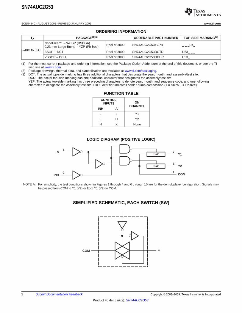
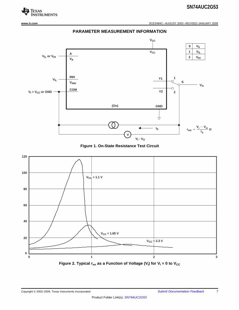
NOTE A: For simplicity, the test conditions shown in Figures 1 through 4 and 6 through 10 are for the demultiplexer configuration. Signals maybe passed from COM to Y1 (Y2) or from Y1 (Y2) to COM.
COM Y
SN74AUC2G53
SCES484C–AUGUST 2003–REVISED JANUARY 2009 ................................................................................................................................................ www.ti.com
ORDERING INFORMATIONTA PACKAGE (1) (2) ORDERABLE PART NUMBER TOP-SIDE MARKING (3)
NanoFree™ – WCSP (DSBGA) Reel of 3000 SN74AUC2G53YZPR _ _ _U4_0.23-mm Large Bump – YZP (Pb-free)–40C to 85C SSOP – DCT Reel of 3000 SN74AUC2G53DCTR U53_ _ _
VSSOP – DCU Reel of 3000 SN74AUC2G53DCUR U53_
(1) For the most current package and ordering information, see the Package Option Addendum at the end of this document, or see the TIweb site at www.ti.com.
(2) Package drawings, thermal data, and symbolization are available at www.ti.com/packaging.(3) DCT: The actual top-side marking has three additional characters that designate the year, month, and assembly/test site.
DCU: The actual top-side marking has one additional character that designates the assembly/test site.YZP: The actual top-side marking has three preceding characters to denote year, month, and sequence code, and one followingcharacter to designate the assembly/test site. Pin 1 identifier indicates solder-bump composition (1 = SnPb, • = Pb-free).
FUNCTION TABLECONTROL
ONINPUTSCHANNEL
INH AL L Y1L H Y2H X None
LOGIC DIAGRAM (POSITIVE LOGIC)
SIMPLIFIED SCHEMATIC, EACH SWITCH (SW)
2 Submit Documentation Feedback Copyright © 2003–2009, Texas Instruments Incorporated
Product Folder Link(s): SN74AUC2G53

Absolute Maximum Ratings (1)
Recommended Operating Conditions (1)
Electrical Characteristics
SN74AUC2G53
www.ti.com ................................................................................................................................................ SCES484C–AUGUST 2003–REVISED JANUARY 2009
over operating free-air temperature range (unless otherwise noted)
MIN MAX UNITVCC Supply voltage range (2) –0.5 3.6 VVI Input voltage range (2) (3) –0.5 3.6 VVI/O Switch I/O voltage range (2) (3) –0.5 VCC + 0.5 VIIK Control input clamp current VI < 0 –50 mAII/OK I/O port diode current VI/O < 0 or VI/O > VCC 50 mAIT On-state switch current current VI/O = 0 to VCC 50 mA
Continuous current through VCC or GND 100 mADCT package 220
θJA Package thermal impedance (4) DCU package 227 C/WYZP package 102
Tstg Storage temperature range –65 150 C
(1) Stresses beyond those listed under "absolute maximum ratings" may cause permanent damage to the device. These are stress ratingsonly, and functional operation of the device at these or any other conditions beyond those indicated under "recommended operatingconditions" is not implied. Exposure to absolute-maximum-rated conditions for extended periods may affect device reliability.
(2) All voltages are with respect to ground unless otherwise specified.(3) The input negative-voltage and output voltage ratings may be exceeded if the input and output current ratings are observed.(4) The package thermal impedance is calculated in accordance with JESD 51-7.
MIN MAX UNITVCC Supply voltage 0.8 2.7 V
VCC = 0.8 V VCC
VIH High-level input voltage VCC = 1.1 V to 1.95 V 0.65 VCCנ VVCC = 2.3 V to 2.7 V 1.7VCC = 0.8 V 0
VIL Low-level input voltage VCC = 1.1 V to 1.95 V 0.35 VCCנ VVCC = 2.3 V to 2.7 V 0.7
VI/O I/O port voltage 0 VCC VVI Control input voltage 0 3.6 V
VCC = 0.8 V to 1.6 V 20Δt/Δv Input transition rise or fall rate VCC = 1.65 V to 1.95 V 10 ns/V
VCC = 2.3 V to 2.7 V 3.5TA Operating free-air temperature –40 85 C
(1) All unused inputs of the device must be held at VCC or GND to ensure proper device operation. Refer to the TI application report,Implications of Slow or Floating CMOS Inputs, literature number SCBA004.
over recommended operating free-air temperature range (unless otherwise noted)
PARAMETER TEST CONDITIONS VCC MIN TYP (1) MAX UNITVI = VCC or GND, 1.1 V 40
IS = 4 mAVINH = VIL 1.65 V 12.5 20ron On-state switch resistance Ω(see Figure 1 andIS = 8 mA 2.3 V 6 15Figure 2)
VI = VCC to GND, 1.1 V 131 180IS = 4 mAVINH = VIL 1.65 V 32 80ron(p) Peak on resistance Ω(see Figure 1 andIS = 8 mA 2.3 V 15 20Figure 2)
(1) TA = 25C
Copyright © 2003–2009, Texas Instruments Incorporated Submit Documentation Feedback 3
Product Folder Link(s): SN74AUC2G53

Switching Characteristics
Switching Characteristics
SN74AUC2G53
SCES484C–AUGUST 2003–REVISED JANUARY 2009 ................................................................................................................................................ www.ti.com
Electrical Characteristics (continued)over recommended operating free-air temperature range (unless otherwise noted)
PARAMETER TEST CONDITIONS VCC MIN TYP (1) MAX UNITVI = VCC to GND, 1.1 V 4
IS = 4 mADifference of on-state resistance VC = VIH 1.65 V 1Δron Ωbetween switches (see Figure 1 andIS = 8 mA 2.3 V 1Figure 2)
VI = VCC and VO = GND, or 1IS(off) Off-state switch leakage current VI = GND and VO = VCC, 2.7 V µA
0.1 (1)VINH = VIH (see Figure 3)
1VI = VCC or GND, VINH = VIL,IS(on) On-state switch leakage current 2.7 V µAVO = Open (see Figure 4) 0.1 (1)
II Control input current VC = VCC or GND 2.7 V 5 µAICC Supply current VC = VCC or GND 2.7 V 10 µACic Control input capacitance 2.5 V 2 pF
Y 3Cio(off) Switch input/output capacitance 2.5 V pF
COM 4.5Cio(on) Switch input/output capacitance 2.5 V 9 pF
over recommended operating free-air temperature range, CL = 15 pF (unless otherwise noted) (see Figure 5)
VCC = 1.2 V VCC = 1.5 V VCC = 1.8 V VCC = 2.5 VVCC = 0.8 VFROM TO 0.1 V 0.1 V 0.15 V 0.2 VPARAMETER UNIT(INPUT) (OUTPUT)TYP MIN MAX MIN MAX MIN TYP MAX MIN MAX
tpd(1) COM or Y Y or COM 0.3 0.3 0.3 0.2 0.1 ns
ten 9.2 0.5 3.5 0.5 2.2 0.5 1 1.9 0.5 1.8INH COM or Y ns
tdis 8.1 0.5 4.2 0.5 3.2 0.5 1.9 3.4 0.5 2.6ten 9.2 0.5 3.6 0.5 2.3 0.5 1.1 1.9 0.5 1.6
A COM or Y nstdis 10 0.5 3.6 0.5 2.3 0.5 1.1 2 0.5 1.6
(1) The propagation delay is the calculated RC time constant of the typical on-state resistance of the switch and the specified loadcapacitance, when driven by an ideal voltage source (zero output impedance).
over recommended operating free-air temperature range, CL = 30 pF (unless otherwise noted) (see Figure 5)
VCC = 1.8 V VCC = 2.5 VFROM TO 0.15 V 0.2 VPARAMETER UNIT(INPUT) (OUTPUT)
MIN TYP MAX MIN MAXtpd
(1) COM or Y Y or COM 0.4 0.2 nsten 0.5 1.6 3.1 0.5 2.2
INH COM or Y nstdis 0.5 2.2 3.4 0.5 2.2ten 0.5 1.6 3 0.5 2.2
A COM or Y nstdis 0.5 1.6 3 0.5 2.3
(1) The propagation delay is the calculated RC time constant of the typical on-state resistance of the switch and the specified loadcapacitance, when driven by an ideal voltage source (zero output impedance).
4 Submit Documentation Feedback Copyright © 2003–2009, Texas Instruments Incorporated
Product Folder Link(s): SN74AUC2G53

Analog Switch Characteristics
SN74AUC2G53
www.ti.com ................................................................................................................................................ SCES484C–AUGUST 2003–REVISED JANUARY 2009
TA = 25C
FROM TOPARAMETER TEST CONDITIONS VCC TYP UNIT(INPUT) (OUTPUT)0.8 V 901.1 V 101CL = 50 pF, RL = 600 Ω,
fin = sine wave 1.4 V 110(see Figure 6) 1.65 V 122
2.3 V 198Frequency response (1)COM or Y Y or COM MHz(switch ON) 0.8 V >500
1.1 V >500CL = 5 pF, RL = 50 Ω,fin = sine wave 1.4 V >500(see Figure 6) 1.65 V >500
2.3 V >5000.8 V –591.1 V –59CL = 50 pF, RL = 600 Ω,
fin = 1 MHz (sine wave) 1.4 V –59(see Figure 7) 1.65 V –59
2.3 V –60Crosstalk (2)COM or Y Y or COM dB(between switches) 0.8 V –55
1.1 V –55CL = 5 pF, RL = 50 Ω,fin = 1 MHz (sine wave) 1.4 V –55(see Figure 7) 1.65 V –55
2.3 V –550.8 V 0.56
CL = 50 pF, RL = 600 Ω, 1.1 V 0.68Crosstalk fin = 1 MHz (squareINH COM or Y 1.4 V 0.81 mV(control input to signal output) wave)
1.65 V 0.93(see Figure 8)2.3 V 1.50.8 V –601.1 V –60CL = 50 pF, RL = 600 Ω,
fin = 1 MHz (sine wave) 1.4 V –60(see Figure 9) 1.65 V –60
2.3 V –60Feed-through attenuation (3)COM or Y Y or COM dB(switch OFF) 0.8 V –59
1.1 V –59CL = 5 pF, RL = 600 Ω,fin = 1 MHz (sine wave) 1.4 V –59(see Figure 9) 1.65 V –59
2.3 V –59
(1) Adjust fin voltage to obtain 0 dBm at output. Increase fin frequency until dB meter reads –3 dB.(2) Adjust fin voltage to obtain 0 dBm at input.(3) Adjust fin voltage to obtain 0 dBm at input.
Copyright © 2003–2009, Texas Instruments Incorporated Submit Documentation Feedback 5
Product Folder Link(s): SN74AUC2G53

Operating Characteristics
Operating Characteristics
SN74AUC2G53
SCES484C–AUGUST 2003–REVISED JANUARY 2009 ................................................................................................................................................ www.ti.com
Analog Switch Characteristics (continued)TA = 25C
FROM TOPARAMETER TEST CONDITIONS VCC TYP UNIT(INPUT) (OUTPUT)0.8 V 6.191.1 V 0.39CL = 50 pF, RL = 10 kΩ,
fin = 1 kHz (sine wave) 1.4 V 0.06(see Figure 10) 1.65 V 0.02
2.3 V 0.01Sine-wave distortion COM or Y Y or COM %
0.8 V 3.551.1 V 0.38CL = 50 pF, RL = 10 kΩ,
fin = 10 kHz (sine wave) 1.4 V 0.04(see Figure 10) 1.65 V 0.02
2.3 V 0.02
for INH input, TA = 25C
VCC = 0.8 V VCC = 1.2 V VCC = 1.5 V VCC = 1.8 V VCC = 2.5 VTESTPARAMETER UNITCONDITIONS TYP TYP TYP TYP TYPPower dissipationCpd f = 10 MHz 3 3 3 3 3 pFcapacitance
for A input, TA = 25C
VCC = 0.8 V VCC = 1.2 V VCC = 1.5 V VCC = 1.8 V VCC = 2.5 VTESTPARAMETER UNITCONDITIONS TYP TYP TYP TYP TYPOutputs 5.5 5.5 5.5 5.5 5.5Power enabled
Cpd dissipation f = 10 MHz pFOutputscapacitance 0.5 0.5 0.5 0.5 0.5disabled
6 Submit Documentation Feedback Copyright © 2003–2009, Texas Instruments Incorporated
Product Folder Link(s): SN74AUC2G53
PARAMETER MEASUREMENT INFORMATION
VCC
VI = VCC or GND
VO
ron VI VO
IS
VI - VO
GND
V
Y1
IS
(On)
VCC
VIL
Y2
A
VA
VINH
INH
COM
VIL or VIH
S
1
2
VA
VIL
VIH
S1
2
0
20
40
60
80
100
120
0 1 2 3
VCC = 1.65 V
VCC = 1.1 V
VCC = 2.3 V
SN74AUC2G53
www.ti.com ................................................................................................................................................ SCES484C–AUGUST 2003–REVISED JANUARY 2009
Figure 1. On-State Resistance Test Circuit
Figure 2. Typical ron as a Function of Voltage (VI) for VI = 0 to VCC
Copyright © 2003–2009, Texas Instruments Incorporated Submit Documentation Feedback 7
Product Folder Link(s): SN74AUC2G53

PARAMETER MEASUREMENT INFORMATION
VCC
VI
VO
GND
Y1
(Off)
VCC
VIH
Y2
A
VA
VINH
INH
COM
VIL or VIH
S
1
2
VA
VIL
VIH
S1
2A
Condition 1: VI = GND, VO = VCCCondition 2: VI = VCC, VO = GND
VCC
VI
VO
GND
Y1
(On)
VCC
VIL
Y2
A
VA
VINH
INH
COM
VIL or VIH
S
1
2
VA
VIL
VIH
S1
2A
VI = VCC or GND
VO = Open
SN74AUC2G53
SCES484C–AUGUST 2003–REVISED JANUARY 2009 ................................................................................................................................................ www.ti.com
Figure 3. Off-State Switch Leakage-Current Test Circuit
Figure 4. On-State Switch Leakage-Current Test Circuit
8 Submit Documentation Feedback Copyright © 2003–2009, Texas Instruments Incorporated
Product Folder Link(s): SN74AUC2G53

PARAMETER MEASUREMENT INFORMATION
VM
thtsu
From OutputUnder Test
CL(see Note A)
LOAD CIRCUIT
S1VLOAD
Open
GND
RL
RL
Data Input
Timing InputVI
0 V
VI
0 V0 V
tw
Input
VOLTAGE WAVEFORMSSETUP AND HOLD TIMES
VOLTAGE WAVEFORMSPROPAGATION DELAY TIMES
INVERTING AND NONINVERTING OUTPUTS
VOLTAGE WAVEFORMSPULSE DURATION
tPLH
tPHL
tPHL
tPLH
VOH
VOH
VOL
VOL
VI
0 VInput
OutputWaveform 1S1 at VLOAD(see Note B)
OutputWaveform 2
S1 at GND(see Note B)
VOL
VOH
tPZL
tPZH
tPLZ
tPHZ
VLOAD/2
0 V
VOL + V∆
VOH − V∆
≈0 V
VI
VOLTAGE WAVEFORMSENABLE AND DISABLE TIMES
LOW- AND HIGH-LEVEL ENABLING
Output
Output
tPLH/tPHLtPLZ/tPZLtPHZ/tPZH
OpenVLOADGND
TEST S1
NOTES: A. CL includes probe and jig capacitance.B. Waveform 1 is for an output with internal conditions such that the output is low, except when disabled by the output control.
Waveform 2 is for an output with internal conditions such that the output is high, except when disabled by the output control.C. All input pulses are supplied by generators having the following characteristics: PRR ≤ 10 MHz, ZO = 50 Ω, slew rate ≥ 1 V/ns.D. The outputs are measured one at a time, with one transition per measurement.E. tPLZ and tPHZ are the same as tdis.F. tPZL and tPZH are the same as ten.G. tPLH and tPHL are the same as tpd.H. All parameters and waveforms are not applicable to all devices.
OutputControl
VM VM
VM VM
VM VM
VM
VM VM
VM
VM
VM
VI
VM
VM
0.8 V1.2 V ± 0.1 V1.5 V ± 0.1 V1.8 V ± 0.15 V2.5 V ± 0.2 V1.8 V ± 0.15 V2.5 V ± 0.2 V
2 kΩ2 kΩ2 kΩ2 kΩ2 kΩ1 kΩ500 Ω
VCC RL
2 × VCC2 × VCC2 × VCC2 × VCC2 × VCC2 × VCC2 × VCC
VLOAD CL
15 pF15 pF15 pF15 pF15 pF30 pF30 pF
0.1 V0.1 V0.1 V0.15 V0.15 V0.15 V0.15 V
V∆
VCCVCCVCCVCCVCCVCCVCC
VI
VCC/2VCC/2VCC/2VCC/2VCC/2VCC/2VCC/2
VMtr/tf
≤2 ns≤2 ns≤2 ns≤2 ns≤2 ns≤2 ns≤2 ns
INPUTS
SN74AUC2G53
www.ti.com ................................................................................................................................................ SCES484C–AUGUST 2003–REVISED JANUARY 2009
Figure 5. Load Circuit and Voltage Waveforms
Copyright © 2003–2009, Texas Instruments Incorporated Submit Documentation Feedback 9
Product Folder Link(s): SN74AUC2G53

PARAMETER MEASUREMENT INFORMATION
VCC
VO
GND
Y1
(On)
VCC
VIL
Y2
A
VA
VINH
INH
COM
VIL or VIH
S
1
2
VA
VIL
VIH
S1
2
50 Ω
0.1 µF
fin
RL/CL: 600 Ω/50 pFRL/CL: 50 Ω/5 pF
RL CL
VCC/2
VCC
VO1
GND
Y1
VCC
VIL
Y2
VIL or VIH
50 Ω
0.1 µF
fin
CL50 pF
VCC/2Rin600 Ω
RL600 Ω
VO2
CL50 pF
VCC/2
RL600 Ω
VA
VIL
VIH
TEST CONDITION
20log10(VO2/VI)
20log10(VO1/VI)A
VA
VINH
INH
COM
SN74AUC2G53
SCES484C–AUGUST 2003–REVISED JANUARY 2009 ................................................................................................................................................ www.ti.com
Figure 6. Frequency Response (Switch On)
Figure 7. Crosstalk (Between Switches)
10 Submit Documentation Feedback Copyright © 2003–2009, Texas Instruments Incorporated
Product Folder Link(s): SN74AUC2G53

PARAMETER MEASUREMENT INFORMATION
VCC
VO
GND
Y1
(On)
VCC
Y2
VIL or VIH
S
1
2
VA
VIL
VIH
S1
250 Ω
VCC/2Rin600 Ω
VCC/2
CL50 pF
RL600 Ω
A
VA
VINH
INH
COM
VCC
VO
GND
Y1
(Off)
VCC
VIL
Y2
VIL or VIH
S1
2
50 Ω
0.1 µF
fin
RL/CL: 600 Ω/50 pFRL/CL: 50 Ω/5 pF
RL CL
VCC/2
RL
VCC/2
A
VA
VINH
INH
COM
S
1
2
VA
VIL
VIH
SN74AUC2G53
www.ti.com ................................................................................................................................................ SCES484C–AUGUST 2003–REVISED JANUARY 2009
Figure 8. Crosstalk (Control Input, Switch Output)
Figure 9. Feedthrough (Switch Off)
Copyright © 2003–2009, Texas Instruments Incorporated Submit Documentation Feedback 11
Product Folder Link(s): SN74AUC2G53

PARAMETER MEASUREMENT INFORMATION
VCC
VO
GND
Y1
(On)
VCC
VIL
Y2
VIL or VIH
S
1
2
VA
VIL
VIH
S1
2
600 Ω
10 µF
fin
RL10 kΩ
CL50 pF
VCC/2
10 µF
A
VA
VINH
INH
COM
VCC = 0.8 V, VI = 0.7 VP-PVCC = 1.1 V, VI = 1 VP-PVCC = 1.4 V, VI = 1.2 VP-PVCC = 1.65 V, VI = 1.4 VP-PVCC = 2.3 V, VI = 2 VP-P
SN74AUC2G53
SCES484C–AUGUST 2003–REVISED JANUARY 2009 ................................................................................................................................................ www.ti.com
Figure 10. Sine-Wave Distortion
12 Submit Documentation Feedback Copyright © 2003–2009, Texas Instruments Incorporated
Product Folder Link(s): SN74AUC2G53

PACKAGE OPTION ADDENDUM
www.ti.com 17-Aug-2015
Addendum-Page 1
PACKAGING INFORMATION
Orderable Device Status(1)
Package Type PackageDrawing
Pins PackageQty
Eco Plan(2)
Lead/Ball Finish(6)
MSL Peak Temp(3)
Op Temp (°C) Device Marking(4/5)
Samples
SN74AUC2G53DCTR ACTIVE SM8 DCT 8 3000 Green (RoHS& no Sb/Br)
CU NIPDAU Level-1-260C-UNLIM -40 to 85 U53Z
SN74AUC2G53DCTRE4 ACTIVE SM8 DCT 8 3000 Green (RoHS& no Sb/Br)
CU NIPDAU Level-1-260C-UNLIM -40 to 85 U53Z
SN74AUC2G53DCTRG4 ACTIVE SM8 DCT 8 3000 Green (RoHS& no Sb/Br)
CU NIPDAU Level-1-260C-UNLIM -40 to 85 U53Z
SN74AUC2G53DCUR ACTIVE VSSOP DCU 8 3000 Green (RoHS& no Sb/Br)
CU NIPDAU | CU SN Level-1-260C-UNLIM -40 to 85 (U53Q ~ U53R)
SN74AUC2G53DCURG4 ACTIVE VSSOP DCU 8 3000 Green (RoHS& no Sb/Br)
CU NIPDAU Level-1-260C-UNLIM -40 to 85 U53R
SN74AUC2G53YZPR ACTIVE DSBGA YZP 8 3000 Green (RoHS& no Sb/Br)
SNAGCU Level-1-260C-UNLIM -40 to 85 (U47 ~ U4N)
(1) The marketing status values are defined as follows:ACTIVE: Product device recommended for new designs.LIFEBUY: TI has announced that the device will be discontinued, and a lifetime-buy period is in effect.NRND: Not recommended for new designs. Device is in production to support existing customers, but TI does not recommend using this part in a new design.PREVIEW: Device has been announced but is not in production. Samples may or may not be available.OBSOLETE: TI has discontinued the production of the device.
(2) Eco Plan - The planned eco-friendly classification: Pb-Free (RoHS), Pb-Free (RoHS Exempt), or Green (RoHS & no Sb/Br) - please check http://www.ti.com/productcontent for the latest availabilityinformation and additional product content details.TBD: The Pb-Free/Green conversion plan has not been defined.Pb-Free (RoHS): TI's terms "Lead-Free" or "Pb-Free" mean semiconductor products that are compatible with the current RoHS requirements for all 6 substances, including the requirement thatlead not exceed 0.1% by weight in homogeneous materials. Where designed to be soldered at high temperatures, TI Pb-Free products are suitable for use in specified lead-free processes.Pb-Free (RoHS Exempt): This component has a RoHS exemption for either 1) lead-based flip-chip solder bumps used between the die and package, or 2) lead-based die adhesive used betweenthe die and leadframe. The component is otherwise considered Pb-Free (RoHS compatible) as defined above.Green (RoHS & no Sb/Br): TI defines "Green" to mean Pb-Free (RoHS compatible), and free of Bromine (Br) and Antimony (Sb) based flame retardants (Br or Sb do not exceed 0.1% by weightin homogeneous material)
(3) MSL, Peak Temp. - The Moisture Sensitivity Level rating according to the JEDEC industry standard classifications, and peak solder temperature.
(4) There may be additional marking, which relates to the logo, the lot trace code information, or the environmental category on the device.
(5) Multiple Device Markings will be inside parentheses. Only one Device Marking contained in parentheses and separated by a "~" will appear on a device. If a line is indented then it is a continuationof the previous line and the two combined represent the entire Device Marking for that device.

PACKAGE OPTION ADDENDUM
www.ti.com 17-Aug-2015
Addendum-Page 2
(6) Lead/Ball Finish - Orderable Devices may have multiple material finish options. Finish options are separated by a vertical ruled line. Lead/Ball Finish values may wrap to two lines if the finishvalue exceeds the maximum column width.
Important Information and Disclaimer:The information provided on this page represents TI's knowledge and belief as of the date that it is provided. TI bases its knowledge and belief on informationprovided by third parties, and makes no representation or warranty as to the accuracy of such information. Efforts are underway to better integrate information from third parties. TI has taken andcontinues to take reasonable steps to provide representative and accurate information but may not have conducted destructive testing or chemical analysis on incoming materials and chemicals.TI and TI suppliers consider certain information to be proprietary, and thus CAS numbers and other limited information may not be available for release.
In no event shall TI's liability arising out of such information exceed the total purchase price of the TI part(s) at issue in this document sold by TI to Customer on an annual basis.

TAPE AND REEL INFORMATION
*All dimensions are nominal
Device PackageType
PackageDrawing
Pins SPQ ReelDiameter
(mm)
ReelWidth
W1 (mm)
A0(mm)
B0(mm)
K0(mm)
P1(mm)
W(mm)
Pin1Quadrant
SN74AUC2G53DCTR SM8 DCT 8 3000 180.0 13.0 3.35 4.5 1.55 4.0 12.0 Q3
SN74AUC2G53DCUR VSSOP DCU 8 3000 180.0 8.4 2.25 3.35 1.05 4.0 8.0 Q3
SN74AUC2G53DCURG4 VSSOP DCU 8 3000 180.0 8.4 2.25 3.35 1.05 4.0 8.0 Q3
SN74AUC2G53YZPR DSBGA YZP 8 3000 178.0 9.2 1.02 2.02 0.63 4.0 8.0 Q1
PACKAGE MATERIALS INFORMATION
www.ti.com 23-Nov-2017
Pack Materials-Page 1

*All dimensions are nominal
Device Package Type Package Drawing Pins SPQ Length (mm) Width (mm) Height (mm)
SN74AUC2G53DCTR SM8 DCT 8 3000 182.0 182.0 20.0
SN74AUC2G53DCUR VSSOP DCU 8 3000 202.0 201.0 28.0
SN74AUC2G53DCURG4 VSSOP DCU 8 3000 202.0 201.0 28.0
SN74AUC2G53YZPR DSBGA YZP 8 3000 220.0 220.0 35.0
PACKAGE MATERIALS INFORMATION
www.ti.com 23-Nov-2017
Pack Materials-Page 2


MECHANICAL DATA
MPDS049B – MAY 1999 – REVISED OCTOBER 2002
POST OFFICE BOX 655303 • DALLAS, TEXAS 75265
DCT (R-PDSO-G8) PLASTIC SMALL-OUTLINE PACKAGE
ÇÇÇÇÇÇÇÇÇÇÇÇÇÇÇÇÇÇÇÇ
0,600,20
0,25
0° – 8°
0,15 NOM
Gage Plane
4188781/C 09/02
4,25
5
0,300,15
2,903,752,70
8
4
3,152,75
1
0,100,00
1,30 MAX
Seating Plane
0,10
M0,130,65
PIN 1INDEX AREA
NOTES: A. All linear dimensions are in millimeters.B. This drawing is subject to change without notice.C. Body dimensions do not include mold flash or protrusionD. Falls within JEDEC MO-187 variation DA.


www.ti.com
PACKAGE OUTLINE
C0.5 MAX
0.190.15
1.5TYP
0.5 TYP
8X 0.250.21
0.5TYP
B E A
D
4223082/A 07/2016
DSBGA - 0.5 mm max heightYZP0008DIE SIZE BALL GRID ARRAY
NOTES: 1. All linear dimensions are in millimeters. Any dimensions in parenthesis are for reference only. Dimensioning and tolerancing per ASME Y14.5M.2. This drawing is subject to change without notice.
BALL A1CORNER
SEATING PLANE
BALL TYP0.05 C
B
1 2
0.015 C A B
SYMM
SYMM
C
A
D
SCALE 8.000
D: Max =
E: Max =
1.918 mm, Min =
0.918 mm, Min =
1.858 mm
0.858 mm

www.ti.com
EXAMPLE BOARD LAYOUT
8X ( 0.23)(0.5) TYP
(0.5) TYP
( 0.23)METAL
0.05 MAX ( 0.23)SOLDER MASKOPENING
0.05 MIN
4223082/A 07/2016
DSBGA - 0.5 mm max heightYZP0008DIE SIZE BALL GRID ARRAY
NOTES: (continued) 3. Final dimensions may vary due to manufacturing tolerance considerations and also routing constraints. For more information, see Texas Instruments literature number SNVA009 (www.ti.com/lit/snva009).
SYMM
SYMM
LAND PATTERN EXAMPLESCALE:40X
1 2
A
B
C
D
NON-SOLDER MASKDEFINED
(PREFERRED)
SOLDER MASK DETAILSNOT TO SCALE
SOLDER MASKOPENING
SOLDER MASKDEFINED
METAL UNDERSOLDER MASK

www.ti.com
EXAMPLE STENCIL DESIGN
(0.5)TYP
(0.5) TYP
8X ( 0.25) (R0.05) TYP
METALTYP
4223082/A 07/2016
DSBGA - 0.5 mm max heightYZP0008DIE SIZE BALL GRID ARRAY
NOTES: (continued) 4. Laser cutting apertures with trapezoidal walls and rounded corners may offer better paste release.
SYMM
SYMM
SOLDER PASTE EXAMPLEBASED ON 0.1 mm THICK STENCIL
SCALE:40X
1 2
A
B
C
D

IMPORTANT NOTICE
Texas Instruments Incorporated (TI) reserves the right to make corrections, enhancements, improvements and other changes to itssemiconductor products and services per JESD46, latest issue, and to discontinue any product or service per JESD48, latest issue. Buyersshould obtain the latest relevant information before placing orders and should verify that such information is current and complete.TI’s published terms of sale for semiconductor products (http://www.ti.com/sc/docs/stdterms.htm) apply to the sale of packaged integratedcircuit products that TI has qualified and released to market. Additional terms may apply to the use or sale of other types of TI products andservices.Reproduction of significant portions of TI information in TI data sheets is permissible only if reproduction is without alteration and isaccompanied by all associated warranties, conditions, limitations, and notices. TI is not responsible or liable for such reproduceddocumentation. Information of third parties may be subject to additional restrictions. Resale of TI products or services with statementsdifferent from or beyond the parameters stated by TI for that product or service voids all express and any implied warranties for theassociated TI product or service and is an unfair and deceptive business practice. TI is not responsible or liable for any such statements.Buyers and others who are developing systems that incorporate TI products (collectively, “Designers”) understand and agree that Designersremain responsible for using their independent analysis, evaluation and judgment in designing their applications and that Designers havefull and exclusive responsibility to assure the safety of Designers' applications and compliance of their applications (and of all TI productsused in or for Designers’ applications) with all applicable regulations, laws and other applicable requirements. Designer represents that, withrespect to their applications, Designer has all the necessary expertise to create and implement safeguards that (1) anticipate dangerousconsequences of failures, (2) monitor failures and their consequences, and (3) lessen the likelihood of failures that might cause harm andtake appropriate actions. Designer agrees that prior to using or distributing any applications that include TI products, Designer willthoroughly test such applications and the functionality of such TI products as used in such applications.TI’s provision of technical, application or other design advice, quality characterization, reliability data or other services or information,including, but not limited to, reference designs and materials relating to evaluation modules, (collectively, “TI Resources”) are intended toassist designers who are developing applications that incorporate TI products; by downloading, accessing or using TI Resources in anyway, Designer (individually or, if Designer is acting on behalf of a company, Designer’s company) agrees to use any particular TI Resourcesolely for this purpose and subject to the terms of this Notice.TI’s provision of TI Resources does not expand or otherwise alter TI’s applicable published warranties or warranty disclaimers for TIproducts, and no additional obligations or liabilities arise from TI providing such TI Resources. TI reserves the right to make corrections,enhancements, improvements and other changes to its TI Resources. TI has not conducted any testing other than that specificallydescribed in the published documentation for a particular TI Resource.Designer is authorized to use, copy and modify any individual TI Resource only in connection with the development of applications thatinclude the TI product(s) identified in such TI Resource. NO OTHER LICENSE, EXPRESS OR IMPLIED, BY ESTOPPEL OR OTHERWISETO ANY OTHER TI INTELLECTUAL PROPERTY RIGHT, AND NO LICENSE TO ANY TECHNOLOGY OR INTELLECTUAL PROPERTYRIGHT OF TI OR ANY THIRD PARTY IS GRANTED HEREIN, including but not limited to any patent right, copyright, mask work right, orother intellectual property right relating to any combination, machine, or process in which TI products or services are used. Informationregarding or referencing third-party products or services does not constitute a license to use such products or services, or a warranty orendorsement thereof. Use of TI Resources may require a license from a third party under the patents or other intellectual property of thethird party, or a license from TI under the patents or other intellectual property of TI.TI RESOURCES ARE PROVIDED “AS IS” AND WITH ALL FAULTS. TI DISCLAIMS ALL OTHER WARRANTIES ORREPRESENTATIONS, EXPRESS OR IMPLIED, REGARDING RESOURCES OR USE THEREOF, INCLUDING BUT NOT LIMITED TOACCURACY OR COMPLETENESS, TITLE, ANY EPIDEMIC FAILURE WARRANTY AND ANY IMPLIED WARRANTIES OFMERCHANTABILITY, FITNESS FOR A PARTICULAR PURPOSE, AND NON-INFRINGEMENT OF ANY THIRD PARTY INTELLECTUALPROPERTY RIGHTS. TI SHALL NOT BE LIABLE FOR AND SHALL NOT DEFEND OR INDEMNIFY DESIGNER AGAINST ANY CLAIM,INCLUDING BUT NOT LIMITED TO ANY INFRINGEMENT CLAIM THAT RELATES TO OR IS BASED ON ANY COMBINATION OFPRODUCTS EVEN IF DESCRIBED IN TI RESOURCES OR OTHERWISE. IN NO EVENT SHALL TI BE LIABLE FOR ANY ACTUAL,DIRECT, SPECIAL, COLLATERAL, INDIRECT, PUNITIVE, INCIDENTAL, CONSEQUENTIAL OR EXEMPLARY DAMAGES INCONNECTION WITH OR ARISING OUT OF TI RESOURCES OR USE THEREOF, AND REGARDLESS OF WHETHER TI HAS BEENADVISED OF THE POSSIBILITY OF SUCH DAMAGES.Unless TI has explicitly designated an individual product as meeting the requirements of a particular industry standard (e.g., ISO/TS 16949and ISO 26262), TI is not responsible for any failure to meet such industry standard requirements.Where TI specifically promotes products as facilitating functional safety or as compliant with industry functional safety standards, suchproducts are intended to help enable customers to design and create their own applications that meet applicable functional safety standardsand requirements. Using products in an application does not by itself establish any safety features in the application. Designers mustensure compliance with safety-related requirements and standards applicable to their applications. Designer may not use any TI products inlife-critical medical equipment unless authorized officers of the parties have executed a special contract specifically governing such use.Life-critical medical equipment is medical equipment where failure of such equipment would cause serious bodily injury or death (e.g., lifesupport, pacemakers, defibrillators, heart pumps, neurostimulators, and implantables). Such equipment includes, without limitation, allmedical devices identified by the U.S. Food and Drug Administration as Class III devices and equivalent classifications outside the U.S.TI may expressly designate certain products as completing a particular qualification (e.g., Q100, Military Grade, or Enhanced Product).Designers agree that it has the necessary expertise to select the product with the appropriate qualification designation for their applicationsand that proper product selection is at Designers’ own risk. Designers are solely responsible for compliance with all legal and regulatoryrequirements in connection with such selection.Designer will fully indemnify TI and its representatives against any damages, costs, losses, and/or liabilities arising out of Designer’s non-compliance with the terms and provisions of this Notice.
Mailing Address: Texas Instruments, Post Office Box 655303, Dallas, Texas 75265Copyright © 2017, Texas Instruments Incorporated


![Taller [DCU] 2012 › 2012 › 05 › definicic3b3n-… · Muéstrame / Dibújame / 5 Porqués Taller [DCU] INMERSIÓN EN SUS VIDAS. Taller [DCU] Taller [DCU] PERFIL DE USUARIO](https://img.dokumen.tips/doc/110x75/5f289122455fd67b955d58d4/taller-dcu-2012-a-2012-a-05-a-definicic3b3n-mustrame-dibjame-.jpg)