Embed Size (px)
Citation preview

CC1000
SWRS048A Page 1 of 55
CC1000 Single Chip Very Low Power RF Transceiver Applications • Very low power UHF wireless data
transmitters and receivers • 315 / 433 / 868 and 915 MHz ISM/SRD
band systems • RKE – Two-way Remote Keyless Entry
• Home automation • Wireless alarm and security systems • AMR – Automatic Meter Reading • Low power telemetry • Game Controllers and advanced toys
Product Description CC1000 is a true single-chip UHF trans-ceiver designed for very low power and very low voltage wireless applications. The circuit is mainly intended for the ISM (Industrial, Scientific and Medical) and SRD (Short Range Device) frequency bands at 315, 433, 868 and 915 MHz, but can easily be programmed for operation at other frequencies in the 300-1000 MHz range. The main operating parameters of CC1000 can be programmed via a serial bus, thus making CC1000 a very flexible and easy to use transceiver. In a typical system CC1000 will be used together with a microcontroller and a few external passive components.
CC1000 is based on Chipcon’s SmartRF® technology in 0.35 µm CMOS.
Features • True single chip UHF RF transceiver • Very low current consumption • Frequency range 300 – 1000 MHz • Integrated bit synchroniser • High sensitivity (typical -110 dBm at 2.4
kBaud) • Programmable output power –20 to
10 dBm • Small size (TSSOP-28 or UltraCSP™
package) • Low supply voltage (2.1 V to 3.6 V) • Very few external components required • No external RF switch / IF filter
required
• RSSI output • Single port antenna connection • FSK data rate up to 76.8 kBaud • Complies with EN 300 220 and FCC
CFR47 part 15 • Programmable frequency in 250 Hz
steps makes crystal temperature drift compensation possible without TCXO
• Suitable for frequency hopping protocols
• Development kit available • Easy-to-use software for generating the
CC1000 configuration data

CC1000
SWRS048A Page 2 of 55
Table of Contents
CC1000........................................................................................................................... 1
Single Chip Very Low Power RF Transceiver........................................................... 1
1. Absolute Maximum Ratings................................................................................... 4
2. Operating Conditions ............................................................................................. 4
3. Electrical Specifications......................................................................................... 4
4. Pin Assignment....................................................................................................... 8
5. Circuit Description.................................................................................................. 9
6. Application Circuit ................................................................................................ 10 6.1 Input / output matching............................................................................................... 10 6.2 VCO inductor.............................................................................................................. 10 6.3 Additional filtering....................................................................................................... 10 6.4 Power supply decoupling ........................................................................................... 10
7. Configuration Overview ....................................................................................... 12
8. Configuration Software ........................................................................................ 12
9. 3-wire Serial Configuration Interface .................................................................. 13
Note: The set-up- and hold-times refer to 50% of VDD.......................................... 14
10. Microcontroller Interface.................................................................................... 15 10.1 Connecting the microcontroller ................................................................................ 15
11. Signal interface ................................................................................................... 16 11.1 Manchester encoding and decoding ........................................................................ 16
12. Bit synchroniser and data decision .................................................................. 19
13. Receiver sensitivity versus data rate and frequency separation.................... 22
14. Frequency programming.................................................................................... 23
15. Recommended RX settings for ISM frequencies ............................................. 24
16. VCO ...................................................................................................................... 25
17. VCO and PLL self-calibration............................................................................. 25
18. VCO and LNA current control ............................................................................ 28
19. Power management ............................................................................................ 28

CC1000
SWRS048A Page 3 of 55
20. Input / Output Matching...................................................................................... 31
21. Output power programming .............................................................................. 32
22. RSSI output ......................................................................................................... 33
23. IF output .............................................................................................................. 34
24. Crystal oscillator................................................................................................. 35
25. Optional LC Filter................................................................................................ 36
26. System Considerations and Guidelines............................................................ 37 26.1 SRD regulations ....................................................................................................... 37 26.2 Low cost systems..................................................................................................... 37 26.3 Battery operated systems......................................................................................... 37 26.4 Crystal drift compensation........................................................................................ 37 26.5 High reliability systems............................................................................................. 37 26.6 Frequency hopping spread spectrum systems......................................................... 37
27. PCB Layout Recommendations......................................................................... 38
28. Antenna Considerations..................................................................................... 38
L = 7125 / f ................................................................................................................. 38
29. Configuration registers ...................................................................................... 39
30. Package Description (TSSOP-28) ...................................................................... 48
31. Package Description (UltraCSP™) .................................................................... 49
32. Plastic Tube Specification ................................................................................. 51
33. Waffle Pack Specification .................................................................................. 51
34. Carrier Tape and Reel Specification.................................................................. 51
35. Ordering Information .......................................................................................... 52
36. General Information............................................................................................ 52 36.1 Document Revision History ...................................................................................... 52 36.2 Product Status Definitions........................................................................................ 52
37. Address Information........................................................................................... 54
38. TI Worldwide Technical Support ....................................................................... 54
39. Product Information Centers ............................................................................. 54

CC1000
SWRS048A Page 4 of 55
1. Absolute Maximum Ratings
Parameter Min. Max. Units Condition Supply voltage, VDD -0.3 5.0 V Voltage on any pin -0.3 VDD+0.3,
max 5.0 V
Input RF level 10 dBm Storage temperature range (TSSOP)
-50 150 °C
Shelf life (UltraCSP™) 1 year Room temperature and oxygen free cabinet
Reflow soldering temperature (TSSOP)
260 °C IPC/JEDEC J-STD-020C
Peak reflow soldering temperature (UltraCSP™)
255 °C IPC/JEDEC J-STD-020C
Under no circumstances the absolute maximum ratings given above should be violated. Stress exceeding one or more of
the limiting values may cause permanent damage to the device.
Caution! ESD sensitive device. Precaution should be used when handling the device in order to prevent permanent damage.
2. Operating Conditions
Parameter
Min. Typ. Max. Unit Condition / Note
RF Frequency Range 300
1000 MHz Programmable in steps of 250 Hz
Operating ambient temperature range -40 85 °C
Supply voltage
2.1 3.0 3.6 V
Note: The same supply voltage should be used for digital (DVDD) and analogue (AVDD) power.
3. Electrical Specifications Tc = 25°C, VDD = 3.0 V if nothing else stated
Parameter
Min. Typ. Max. Unit Condition / Note
Transmit Section
Transmit data rate
0.6 76.8 kBaud NRZ or Manchester encoding. 76.8 kBaud equals 76.8 kbit/s using NRZ coding. See page 16.
Binary FSK frequency separation
0 65 kHz The frequency separation is programmable in 250 Hz steps. 65 kHz is the maximum guaranteed separation at 1 MHz reference frequency. Larger separations can be achieved at higher reference frequencies.
CC1000
SWRS048A Page 5 of 55
Parameter
Min. Typ. Max. Unit Condition / Note
Output power 433 MHz 868 MHz
-20 -20
10 5
dBm dBm
Delivered to 50 Ω load. The output power is programmable.
RF output impedance 433/868 MHz
140 / 80 Ω Transmit mode. For matching details see “Input/ output matching” p.31.
Harmonics
-20 dBc An external LC or SAW filter should be used to reduce harmonics emission to comply with SRD requirements. See p.36.
Receive Section
Receiver Sensitivity, 433 MHz Optimum sensitivity (9.3 mA) Low current consumption (7.4 mA) Receiver Sensitivity, 868 MHz Optimum sensitivity (11.8 mA) Low current consumption (9.6 mA)
-110 -109
-107 -105
dBm dBm
dBm dBm
2.4 kBaud, Manchester coded data, 64 kHz frequency separation, BER = 10-3 See Table 6 and Table 7 page 22 for typical sensitivity figures at other data rates.
System noise bandwidth 30 kHz 2.4 kBaud, Manchester coded data
Cascaded noise figure 433/868 MHz
12/13 dB
Saturation
10 dBm 2.4 kBaud, Manchester coded data, BER = 10-3
Input IP3
-18 dBm From LNA to IF output
Blocking
40 dBc At +/- 1 MHz
LO leakage -57 dBm
Input impedance 88-j26 70-j26 52-j7 52-j4
Ω Ω Ω Ω
Receive mode, series equivalent at 315 MHz at 433 MHz at 868 MHz. At 915 MHz For matching details see “Input/ output matching” p. 31.
Turn on time 11 128 Baud The turn-on time is determined by the demodulator settling time, which is programmable. See p. 19
IF Section
Intermediate frequency (IF)
150 10.7
kHz MHz
Internal IF filter External IF filter
IF bandwidth
175 kHz
RSSI dynamic range
-105 -50 dBm
RSSI accuracy ± 6
dB
See p.33 for details
RSSI linearity ± 2 dB

CC1000
SWRS048A Page 6 of 55
Parameter
Min. Typ. Max. Unit Condition / Note
Frequency Synthesiser Section
Crystal Oscillator Frequency
3 16 MHz Crystal frequency can be 3-4, 6-8 or 9-16 MHz. Recommended frequencies are 3.6864, 7.3728, 11.0592 and 14.7456. See page 35 for details.
Crystal frequency accuracy requirement
± 50 ± 25
ppm 433 MHz 868 MHz The crystal frequency accuracy and drift (ageing and temperature dependency) will determine the frequency accuracy of the transmitted signal.
Crystal operation
Parallel
C171 and C181 are loading capacitors, see page 35
Crystal load capacitance
12 12 12
22 16 16
30 30 16
pF pF pF
3-4 MHz, 22 pF recommended 6-8 MHz, 16 pF recommended 9-16 MHz, 16 pF recommended
Crystal oscillator start-up time 5 1.5 2
ms ms ms
3.6864 MHz, 16 pF load 7.3728 MHz, 16 pF load 16 MHz, 16 pF load
Output signal phase noise
-85 dBc/Hz At 100 kHz offset from carrier
PLL lock time (RX / TX turn time)
200 µs Up to 1 MHz frequency step
PLL turn-on time, crystal oscillator on in power down mode
250 µs Crystal oscillator running
Digital Inputs/Outputs
Logic “0” input voltage
0 0.3*VDD V
Logic ”1” input voltage
0.7*VDD VDD V
Logic “0” output voltage
0
0.4 V Output current -2.5 mA, 3.0 V supply voltage
Logic “1” output voltage
2.5
VDD V Output current 2.5 mA, 3.0 V supply voltage
Logic “0” input current
NA -1 µA Input signal equals GND
Logic “1” input current
NA 1 µA Input signal equals VDD
DIO setup time
20 ns TX mode, minimum time DIO must be ready before the positive edge of DCLK
DIO hold time
10 ns TX mode, minimum time DIO must be held after the positive edge of DCLK
Serial interface (PCLK, PDATA and PALE) timing specification
See Table 2 page 14
Current Consumption
Power Down mode
0.2 1 µA Oscillator core off
CC1000
SWRS048A Page 7 of 55
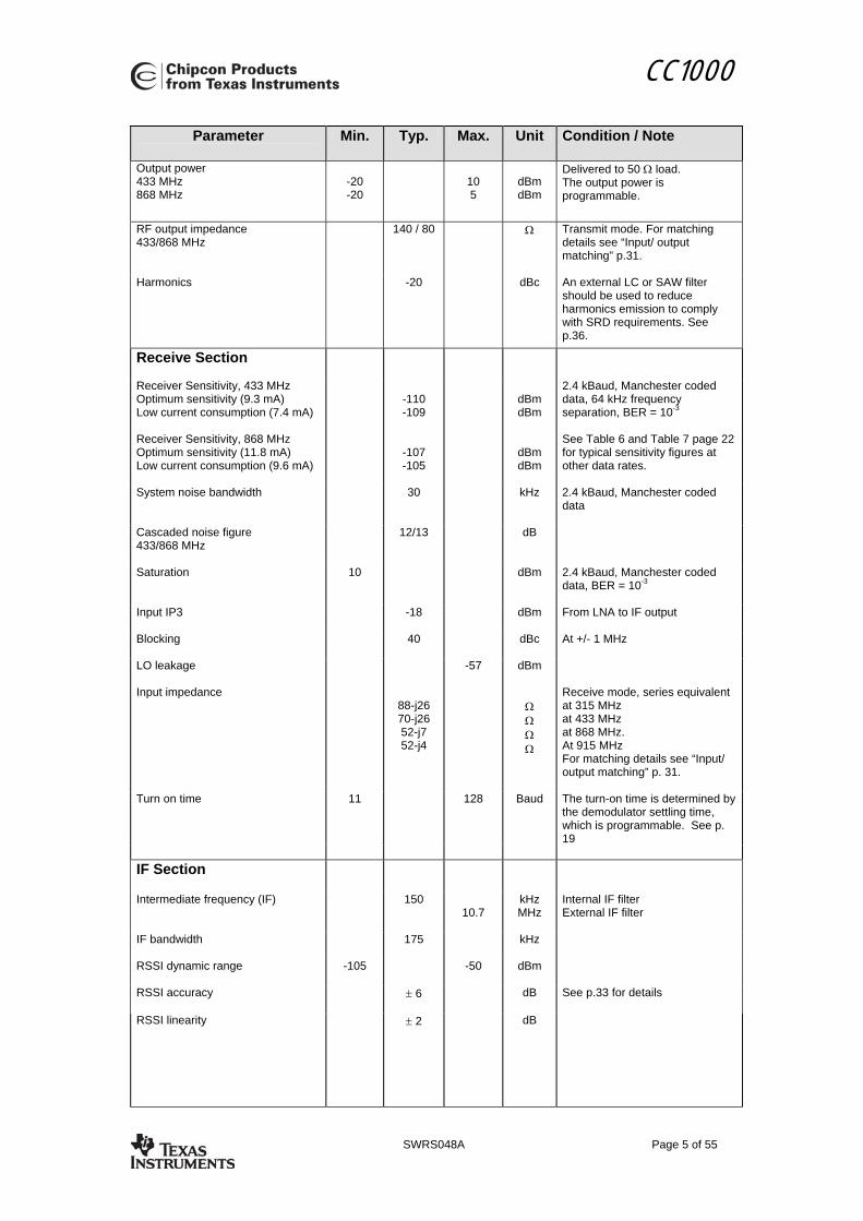
Parameter
Min. Typ. Max. Unit Condition / Note
Current Consumption, receive mode 433/868 MHz
7.4/9.6 mA Current is programmable and can be increased for improved sensitivity
Current Consumption, average in receive mode using polling 433/868 MHz
74/96 µA Polling controlled by micro-controller using 1:100 receive to power down ratio
Current Consumption, transmit mode 433/868 MHz: P=0.01mW (-20 dBm) P=0.3 mW (-5 dBm) P=1 mW (0 dBm) P=3 mW (5 dBm) P=10 mW (10 dBm)
5.3/8.6
8.9/13.8
10.4/16.5
14.8/25.4
26.7/NA
mA
mA
mA
mA
mA
The ouput power is delivered to a 50Ω load, see also p. 32
Current Consumption, crystal osc. Current Consumption, crystal osc. And bias Current Consumption, crystal osc., bias and synthesiser, RX/TX
30 80
105
860
4/5 5/6
µA µA µA
µA
mA mA
3-8 MHz, 16 pF load 9-14 MHz, 12 pF load 14-16 MHz, 16 pF load < 500 MHz > 500 MHz
CC1000
SWRS048A Page 8 of 55
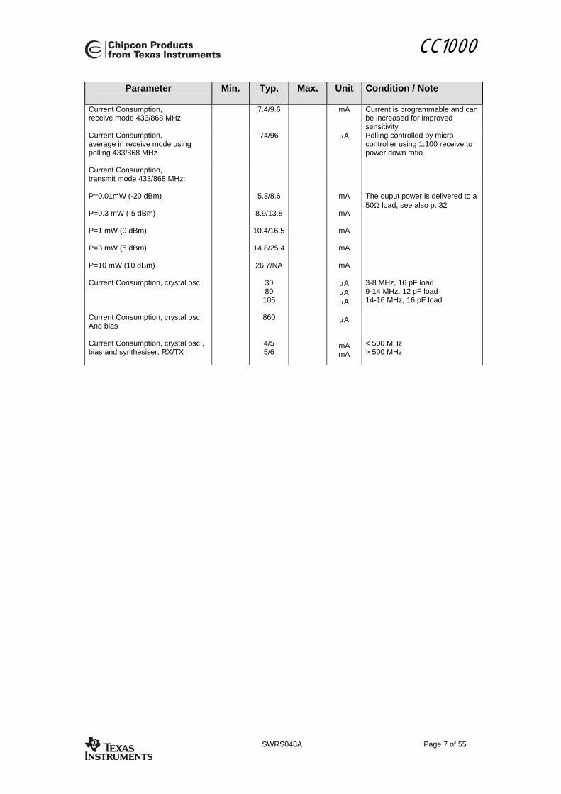
4. Pin Assignment
Pin no. UltraCSP pin no.
Pin name Pin type Description
1 G3 AVDD Power (A) Power supply (3 V) for analog modules (mixer and IF) 2 F2 AGND Ground (A) Ground connection (0 V) for analog modules (mixer and IF) 3 G2 RF_IN RF Input RF signal input from antenna 4 G1 RF_OUT RF output RF signal output to antenna 5 F1 AVDD Power (A) Power supply (3 V) for analog modules (LNA and PA) 6 E2 AGND Ground (A) Ground connection (0 V) for analog modules (LNA and PA) 7 E1 AGND Ground (A) Ground connection (0 V) for analog modules (PA) 8 D1 AGND Ground (A) Ground connection (0 V) for analog modules (VCO and prescaler) 9 C1 AVDD Power (A) Power supply (3 V) for analog modules (VCO and prescaler)
10 B1 L1 Analog input Connection no 1 for external VCO tank inductor 11 A1 L2 Analog input Connection no 2 for external VCO tank inductor 12 B2 CHP_OUT
(LOCK) Analog output Charge pump current output
The pin can also be used as PLL Lock indicator. Output is high when PLL is in lock.
13 C2 R_BIAS Analog output Connection for external precision bias resistor (82 kΩ, ± 1%) 14 F3 AGND Ground (A) Ground connection (0 V) for analog modules (backplane) 15 A2 AVDD Power (A) Power supply (3 V) for analog modules (general) 16 B3 AGND Ground (A) Ground connection (0 V) for analog modules (general) 17 A3 XOSC_Q2 Analog output Crystal, pin 2 18 A4 XOSC_Q1 Analog input Crystal, pin 1, or external clock input 19 B4 AGND Ground (A) Ground connection (0 V) for analog modules (guard) 20 C3 DGND Ground (D) Ground connection (0 V) for digital modules (substrate) 21 C4 DVDD Power (D) Power supply (3 V) for digital modules 22 D4 DGND Ground (D) Ground connection (0 V) for digital modules 23 E4 DIO Digital
input/output Data input/output. Data input in transmit mode. Data output in receive mode
24 F4 DCLK Digital output Data clock for data in both receive and transmit mode 25 G4 PCLK Digital input Programming clock for 3-wire bus 26 D3 PDATA Digital
input/output Programming data for 3-wire bus. Programming data input for write operation, programming data output for read operation
27 D2 PALE Digital input Programming address latch enable for 3-wire bus. Internal pull-up. 28 E3 RSSI/IF Analog output The pin can be used as RSSI or 10.7 MHz IF output to optional
external IF and demodulator. If not used, the pin should be left open (not connected).
A=Analog, D=Digital (Top View)
1
14 15
AVDD
AGND
RF_IN
RF_OUT
AVDD
AGND
AGND
AGND
AVDD
L1
L2
R_BIAS
CHP_OUT
AGND
CC1000
2
3
4
6
5
7
8
9
11
12
13
10
28 RSSI/IF
PALE
PDATA
PCLK
DCLK
DIO
DGND
DVDD
DGND
AGND
XOSC_Q1
AGND
XOSC_Q2
AVDD
27
26
25
23
24
22
21
20
18
17
16
19
1
14 15
AVDD
AGND
RF_IN
RF_OUT
AVDD
AGND
AGND
AGND
AVDD
L1
L2
R_BIAS
CHP_OUT
AGND
CC1000
2
3
4
6
5
7
8
9
11
12
13
10
28 RSSI/IF
PALE
PDATA
PCLK
DCLK
DIO
DGND
DVDD
DGND
AGND
XOSC_Q1
AGND
XOSC_Q2
AVDD
RSSI/IF
PALE
PDATA
PCLK
DCLK
DIO
DGND
DVDD
DGND
AGND
XOSC_Q1
AGND
XOSC_Q2
AVDD
27
26
25
23
24
22
21
20
18
17
16
19

CC1000
SWRS048A Page 9 of 55
5. Circuit Description
Figure 1. Simplified block diagram of the CC1000
A simplified block diagram of CC1000 is shown in Figure 1. Only signal pins are shown. In receive mode CC1000 is configured as a traditional superheterodyne receiver. The RF input signal is amplified by the low-noise amplifier (LNA) and converted down to the intermediate frequency (IF) by the mixer (MIXER). In the intermediate frequency stage (IF STAGE) this downconverted signal is amplified and filtered before being fed to the demodulator (DEMOD). As an option a RSSI signal, or the IF signal after the mixer is available at the RSSI/IF pin. After demodulation CC1000 outputs the digital demodulated data on the pin DIO. Synchronisation is done on-chip providing data clock at DCLK.
In transmit mode the voltage controlled oscillator (VCO) output signal is fed directly to the power amplifier (PA). The RF output is frequency shift keyed (FSK) by the digital bit stream fed to the pin DIO. The internal T/R switch circuitry makes the antenna interface and matching very easy. The frequency synthesiser generates the local oscillator signal which is fed to the MIXER in receive mode and to the PA in transmit mode. The frequency synthesiser consists of a crystal oscillator (XOSC), phase detector (PD), charge pump (CHARGE PUMP), VCO, and frequency dividers (/R and /N). An external crystal must be connected to XOSC, and only an external inductor is required for the VCO. The 3-wire digital serial interface (CONTROL) is used for configuration.
PDATA, PCLK, PALE
LNA
PA
DEMOD
VCO PD OSC~/N
MIXER
CHARGEPUMP
L1
RF_IN DIO
CHP_OUT
IF STAGE
RF_OUT
RSSI/IF
3
CONTROL
XOSC_Q2
XOSC_Q1/R
DCLK
L2
LPF
BIAS R_BIAS
PDATA, PCLK, PALE
LNA
PA
DEMOD
VCO PD OSC~/N
MIXER
CHARGEPUMP
L1
RF_IN DIO
CHP_OUT
IF STAGE
RF_OUT
RSSI/IF
3
CONTROL
XOSC_Q2
XOSC_Q1/R
DCLK
L2
LPF
BIAS R_BIAS

CC1000
SWRS048A Page 10 of 55
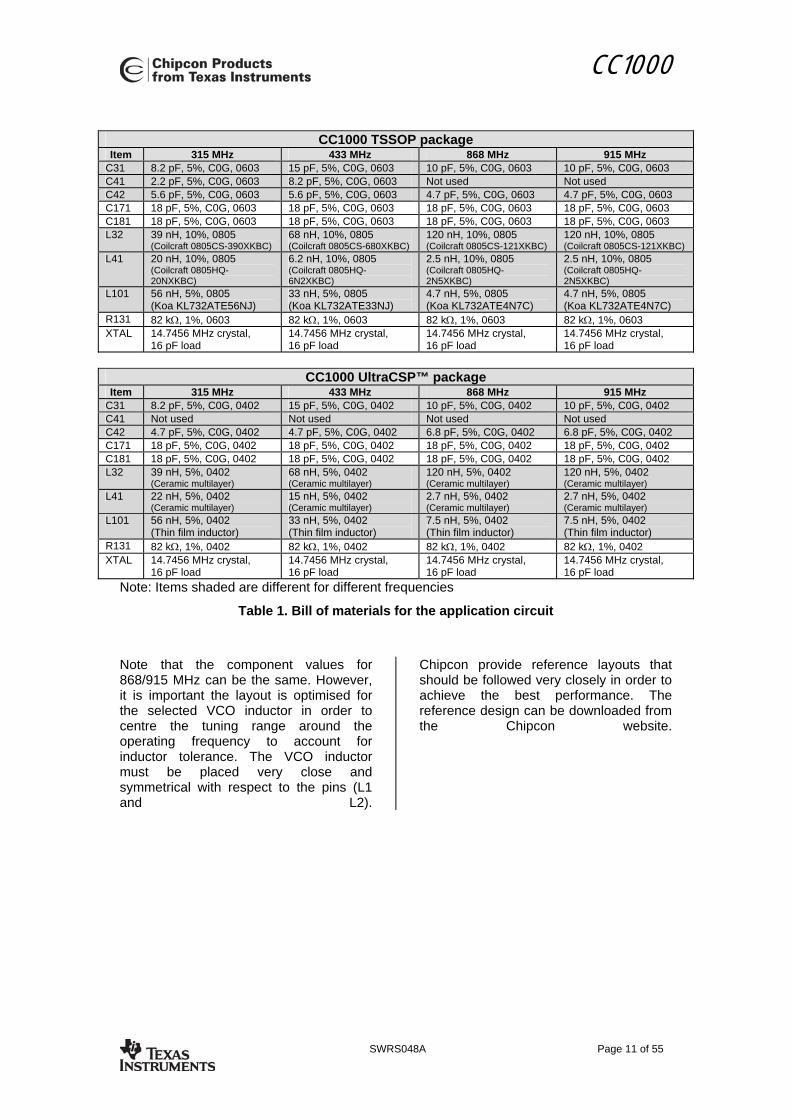
6. Application Circuit Very few external components are required for the operation of CC1000. A typical application circuit is shown in Figure 2. Component values are shown in Table 1. 6.1 Input / output matching C31/L32 is the input match for the receiver. L32 is also a DC choke for biasing. C41, L41 and C42 are used to match the transmitter to 50 Ω. An internal T/R switch circuit makes it possible to connect the input and output together and match the CC1000 to 50 Ω in both RX and TX mode. See “Input/output matching” p.31 for details. 6.2 VCO inductor The VCO is completely integrated except for the inductor L101.
Component values for the matching network and VCO inductor are easily calculated using the SmartRF® Studio software. 6.3 Additional filtering Additional external components (e.g. RF LC or SAW-filter) may be used in order to improve the performance in specific applications. See also “Optional LC filter” p.36 for further information. 6.4 Power supply decoupling Power supply decoupling and filtering must be used (not shown in the application circuit). The placement and size of the decoupling capacitors and the power supply filtering are very important to achieve the optimum performance. Chipcon provides reference designs (CC1000PP and CC1000uCSP_EM) that should be followed very closely.
Figure 2. Typical CC1000 application circuit (power supply decoupling not shown)
CC1000
SWRS048A Page 11 of 55
CC1000 TSSOP package
Item 315 MHz 433 MHz 868 MHz 915 MHz C31 8.2 pF, 5%, C0G, 0603 15 pF, 5%, C0G, 0603 10 pF, 5%, C0G, 0603 10 pF, 5%, C0G, 0603 C41 2.2 pF, 5%, C0G, 0603 8.2 pF, 5%, C0G, 0603 Not used Not used C42 5.6 pF, 5%, C0G, 0603 5.6 pF, 5%, C0G, 0603 4.7 pF, 5%, C0G, 0603 4.7 pF, 5%, C0G, 0603 C171 18 pF, 5%, C0G, 0603 18 pF, 5%, C0G, 0603 18 pF, 5%, C0G, 0603 18 pF, 5%, C0G, 0603 C181 18 pF, 5%, C0G, 0603 18 pF, 5%, C0G, 0603 18 pF, 5%, C0G, 0603 18 pF, 5%, C0G, 0603 L32 39 nH, 10%, 0805
(Coilcraft 0805CS-390XKBC) 68 nH, 10%, 0805 (Coilcraft 0805CS-680XKBC)
120 nH, 10%, 0805 (Coilcraft 0805CS-121XKBC)
120 nH, 10%, 0805 (Coilcraft 0805CS-121XKBC)
L41 20 nH, 10%, 0805 (Coilcraft 0805HQ-20NXKBC)
6.2 nH, 10%, 0805 (Coilcraft 0805HQ-6N2XKBC)
2.5 nH, 10%, 0805 (Coilcraft 0805HQ-2N5XKBC)
2.5 nH, 10%, 0805 (Coilcraft 0805HQ-2N5XKBC)
L101 56 nH, 5%, 0805 (Koa KL732ATE56NJ)
33 nH, 5%, 0805 (Koa KL732ATE33NJ)
4.7 nH, 5%, 0805 (Koa KL732ATE4N7C)
4.7 nH, 5%, 0805 (Koa KL732ATE4N7C)
R131 82 kΩ, 1%, 0603 82 kΩ, 1%, 0603 82 kΩ, 1%, 0603 82 kΩ, 1%, 0603 XTAL 14.7456 MHz crystal,
16 pF load 14.7456 MHz crystal, 16 pF load
14.7456 MHz crystal, 16 pF load
14.7456 MHz crystal, 16 pF load
CC1000 UltraCSP™ package
Item 315 MHz 433 MHz 868 MHz 915 MHz C31 8.2 pF, 5%, C0G, 0402 15 pF, 5%, C0G, 0402 10 pF, 5%, C0G, 0402 10 pF, 5%, C0G, 0402 C41 Not used Not used Not used Not used C42 4.7 pF, 5%, C0G, 0402 4.7 pF, 5%, C0G, 0402 6.8 pF, 5%, C0G, 0402 6.8 pF, 5%, C0G, 0402 C171 18 pF, 5%, C0G, 0402 18 pF, 5%, C0G, 0402 18 pF, 5%, C0G, 0402 18 pF, 5%, C0G, 0402 C181 18 pF, 5%, C0G, 0402 18 pF, 5%, C0G, 0402 18 pF, 5%, C0G, 0402 18 pF, 5%, C0G, 0402 L32 39 nH, 5%, 0402
(Ceramic multilayer) 68 nH, 5%, 0402 (Ceramic multilayer)
120 nH, 5%, 0402 (Ceramic multilayer)
120 nH, 5%, 0402 (Ceramic multilayer)
L41 22 nH, 5%, 0402 (Ceramic multilayer)
15 nH, 5%, 0402 (Ceramic multilayer)
2.7 nH, 5%, 0402 (Ceramic multilayer)
2.7 nH, 5%, 0402 (Ceramic multilayer)
L101 56 nH, 5%, 0402 (Thin film inductor)
33 nH, 5%, 0402 (Thin film inductor)
7.5 nH, 5%, 0402 (Thin film inductor)
7.5 nH, 5%, 0402 (Thin film inductor)
R131 82 kΩ, 1%, 0402 82 kΩ, 1%, 0402 82 kΩ, 1%, 0402 82 kΩ, 1%, 0402 XTAL 14.7456 MHz crystal,
16 pF load 14.7456 MHz crystal, 16 pF load
14.7456 MHz crystal, 16 pF load
14.7456 MHz crystal, 16 pF load
Note: Items shaded are different for different frequencies
Table 1. Bill of materials for the application circuit
Note that the component values for 868/915 MHz can be the same. However, it is important the layout is optimised for the selected VCO inductor in order to centre the tuning range around the operating frequency to account for inductor tolerance. The VCO inductor must be placed very close and symmetrical with respect to the pins (L1 and L2).
Chipcon provide reference layouts that should be followed very closely in order to achieve the best performance. The reference design can be downloaded from the Chipcon website.
CC1000
SWRS048A Page 12 of 55
7. Configuration Overview CC1000 can be configured to achieve the best performance for different applications. Through the programmable configuration registers the following key parameters can be programmed: • Receive / transmit mode • RF output power • Frequency synthesiser key
parameters: RF output frequency, FSK
frequency separation (deviation), crystal oscillator reference frequency
• Power-down / power-up mode • Crystal oscillator power-up / power
down • Data rate and data format (NRZ,
Manchester coded or UART interface) • Synthesiser lock indicator mode • Optional RSSI or external IF
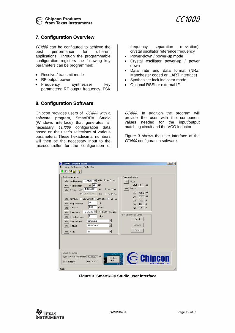
8. Configuration Software Chipcon provides users of CC1000 with a software program, SmartRF® Studio (Windows interface) that generates all necessary CC1000 configuration data based on the user’s selections of various parameters. These hexadecimal numbers will then be the necessary input to the microcontroller for the configuration of
CC1000. In addition the program will provide the user with the component values needed for the input/output matching circuit and the VCO inductor. Figure 3 shows the user interface of the CC1000 configuration software.
Figure 3. SmartRF® Studio user interface
CC1000
SWRS048A Page 13 of 55
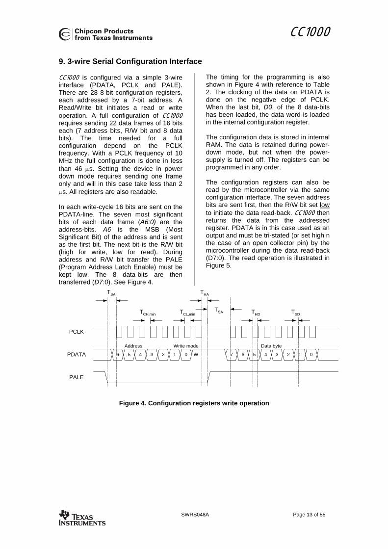
9. 3-wire Serial Configuration Interface CC1000 is configured via a simple 3-wire interface (PDATA, PCLK and PALE). There are 28 8-bit configuration registers, each addressed by a 7-bit address. A Read/Write bit initiates a read or write operation. A full configuration of CC1000 requires sending 22 data frames of 16 bits each (7 address bits, R/W bit and 8 data bits). The time needed for a full configuration depend on the PCLK frequency. With a PCLK frequency of 10 MHz the full configuration is done in less than 46 µs. Setting the device in power down mode requires sending one frame only and will in this case take less than 2 µs. All registers are also readable. In each write-cycle 16 bits are sent on the PDATA-line. The seven most significant bits of each data frame (A6:0) are the address-bits. A6 is the MSB (Most Significant Bit) of the address and is sent as the first bit. The next bit is the R/W bit (high for write, low for read). During address and R/W bit transfer the PALE (Program Address Latch Enable) must be kept low. The 8 data-bits are then transferred (D7:0). See Figure 4.
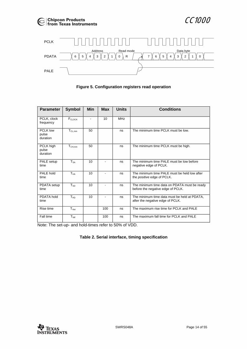
The timing for the programming is also shown in Figure 4 with reference to Table 2. The clocking of the data on PDATA is done on the negative edge of PCLK. When the last bit, D0, of the 8 data-bits has been loaded, the data word is loaded in the internal configuration register. The configuration data is stored in internal RAM. The data is retained during power-down mode, but not when the power-supply is turned off. The registers can be programmed in any order. The configuration registers can also be read by the microcontroller via the same configuration interface. The seven address bits are sent first, then the R/W bit set low to initiate the data read-back. CC1000 then returns the data from the addressed register. PDATA is in this case used as an output and must be tri-stated (or set high n the case of an open collector pin) by the microcontroller during the data read-back (D7:0). The read operation is illustrated in Figure 5.
Figure 4. Configuration registers write operation
PCLK
PDATA
PALE
Address Write mode
6 5 4 3 2 1 0 7 6 5 4 3 2 1 0
Data byte
THD
TSA
TCH,min TCL,min
THA
W
TSDTSA
CC1000
SWRS048A Page 14 of 55
Figure 5. Configuration registers read operation
Parameter Symbol
Min Max Units Conditions
PCLK, clock frequency
FCLOCK
- 10 MHz
PCLK low pulse duration
TCL,min 50 ns The minimum time PCLK must be low.
PCLK high pulse duration
TCH,min 50 ns The minimum time PCLK must be high.
PALE setup time
TSA
10 - ns The minimum time PALE must be low before negative edge of PCLK.
PALE hold time
THA 10 - ns The minimum time PALE must be held low after the positive edge of PCLK.
PDATA setup time
TSD
10 - ns The minimum time data on PDATA must be ready before the negative edge of PCLK.
PDATA hold time
THD 10 - ns The minimum time data must be held at PDATA, after the negative edge of PCLK.
Rise time Trise 100 ns The maximum rise time for PCLK and PALE
Fall time Tfall 100 ns The maximum fall time for PCLK and PALE
Note: The set-up- and hold-times refer to 50% of VDD.
Table 2. Serial interface, timing specification
PCLK
Address Read mode
6 5 4 3 2 1 0 R 7 6 5 4 3 2 1 0
Data byte
PALE
PDATA
CC1000
SWRS048A Page 15 of 55
10. Microcontroller Interface Used in a typical system, CC1000 will interface to a microcontroller. This microcontroller must be able to: • Program CC1000 into different modes
via the 3-wire serial configuration interface (PDATA, PCLK and PALE).
• Interface to the bi-directional synchronous data signal interface (DIO and DCLK).
• Optionally the microcontroller can do data encoding / decoding.
• Optionally the microcontroller can monitor the frequency lock status from pin CHP_OUT (LOCK).
• Optionally the microcontroller can monitor the RSSI output for signal strength acquisition.
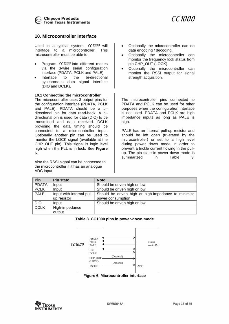
10.1 Connecting the microcontroller The microcontroller uses 3 output pins for the configuration interface (PDATA, PCLK and PALE). PDATA should be a bi-directional pin for data read-back. A bi-directional pin is used for data (DIO) to be transmitted and data received. DCLK providing the data timing should be connected to a microcontroller input. Optionally another pin can be used to monitor the LOCK signal (available at the CHP_OUT pin). This signal is logic level high when the PLL is in lock. See Figure 6. Also the RSSI signal can be connected to the microcontroller if it has an analogue ADC input.
The microcontroller pins connected to PDATA and PCLK can be used for other purposes when the configuration interface is not used. PDATA and PCLK are high impedance inputs as long as PALE is high. PALE has an internal pull-up resistor and should be left open (tri-stated by the microcontroller) or set to a high level during power down mode in order to prevent a trickle current flowing in the pull-up. The pin state in power down mode is summarized in Table 3.
Pin Pin state Note PDATA Input Should be driven high or low PCLK Input Should be driven high or low PALE Input with internal pull-
up resistor Should be driven high or high-impedance to minimize power consumption
DIO Input Should be driven high or low DCLK High-impedance
output
Table 3. CC1000 pins in power-down mode
CC1000PDATAPCLKPALE
DIO
CHP_OUT(LOCK)
Micro-controller
DCLK(Optional)
RSSI/IF(Optional)
ADC
Figure 6. Microcontroller interface
CC1000
SWRS048A Page 16 of 55
11. Signal interface The signal interface consists of DIO and DCLK and is used for the data to be transmitted and data received. DIO is the bi-directional data line and DCLK provides a synchronous clock both during data transmission and data reception. The CC1000 can be used with NRZ (Non-Return-to-Zero) data or Manchester (also known as bi-phase-level) encoded data. CC1000 can also synchronise the data from the demodulator and provide the data clock at DCLK. CC1000 can be configured for three different data formats: Synchronous NRZ mode. In transmit mode CC1000 provides the data clock at DCLK, and DIO is used as data input. Data is clocked into CC1000 at the rising edge of DCLK. The data is modulated at RF without encoding. CC1000 can be configured for the data rates 0.6, 1.2, 2.4, 4.8, 9.6, 19.2, 38.4 or 76.8 kbit/s. For 38.4 and 76.8 kbit/s a crystal frequency of 14.7456 MHz must be used. In receive mode CC1000 does the synchronisation and provides received data clock at DCLK and data at DIO. The data should be clocked into the interfacing circuit at the rising edge of DCLK. See Figure 7. Synchronous Manchester encoded mode. In transmit mode CC1000 provides the data clock at DCLK, and DIO is used as data input. Data is clocked into CC1000 at the rising edge of DCLK and should be in NRZ format. The data is modulated at RF with Manchester code. The encoding is done by CC1000. In this mode CC1000 can be configured for the data rates 0.3, 0.6, 1.2, 2.4, 4.8, 9.6, 19.2 or 38.4 kbit/s. The 38.4 kbit/s rate corresponds to the maximum 76.8 kBaud due to the Manchester encoding. For 38.4 and 76.8 kBaud a crystal frequency of 14.7456 MHz must be used. In receive mode CC1000 does the synchronisation and provides received data clock at DCLK and data at DIO. CC1000 does the decoding and NRZ data
is presented at DIO. The data should be clocked into the interfacing circuit at the rising edge of DCLK. See Figure 8. Transparent Asynchronous UART mode. In transmit mode DIO is used as data input. The data is modulated at RF without synchronisation or encoding. In receive mode the raw data signal from the demodulator is sent to the output. No synchronisation or decoding of the signal is done in CC1000 and should be done by the interfacing circuit. The DCLK pin is used as data output in this mode. Data rates in the range from 0.6 to 76.8 kBaud can be used. For 38.4 and 76.8 kBaud a crystal frequency of 14.7456 MHz must be used. See Figure 9. 11.1 Manchester encoding and decoding In the Synchronous Manchester encoded mode CC1000 uses Manchester coding when modulating the data. The CC1000 also performs the data decoding and synchronisation. The Manchester code is based on transitions; a “0” is encoded as a low-to-high transition, a “1” is encoded as a high-to-low transition. See Figure 10. The CC1000 can detect a Manchester decoding violation and will set a Manchester Violation Flag when such a violation is detected in the incoming signal. The threshold limit for the Manchester Violation can be set in the MODEM1 register. The Manchester Violation Flag can be monitored at the CHP_OUT (LOCK) pin, configured in the LOCK register. The Manchester code ensures that the signal has a constant DC component, which is necessary in some FSK demodulators. Using this mode also ensures compatibility with CC400/CC900 designs.

CC1000
SWRS048A Page 17 of 55
Figure 7. Synchronous NRZ mode
Figure 8. Synchronous Manchester encoded mode
DIO
DCLK
“RF”
Clock provided by CC1000
FSK modulating signal (NRZ),internal in CC1000
Data provided by microcontroller
Transmitter side:
Clock provided by CC1000
Demodulated signal (NRZ),internal in CC1000
Data provided by CC1000
Receiver side:
“RF”
DCLK
DIO
DIO
DCLK
“RF”
Clock provided by CC1000
FSK modulating signal (NRZ),internal in CC1000
Data provided by microcontroller
Transmitter side:
Clock provided by CC1000
Demodulated signal (NRZ),internal in CC1000
Data provided by CC1000
Receiver side:
“RF”
DCLK
DIO
DIO
DCLK
“RF”
Clock provided by CC1000
FSK modulating signal (Manchester encoded),internal in CC1000
Data provided by microcontroller (NRZ)
Transmitter side:
Clock provided by CC1000
Demodulated signal (Manchester encoded),internal in CC1000
Data provided by CC1000 (NRZ)
Receiver side:
“RF”
DCLK
DIO

CC1000
SWRS048A Page 18 of 55
Figure 9. Transparent Asynchronous UART mode
Time
TXdata
1 0 1 1 0 0 0 1 1 0 1
Time
TXdata
1 0 1 1 0 0 0 1 1 0 1
Figure 10. Manchester encoding
DIO
DCLK
“RF”
DCLK is not used in transmit mode. Used as data output in receive mode.
FSK modulating signal,internal in CC1000
Data provided by UART (TXD)
Transmitter side:
DIO is not used in receive mode. Used only as data input in transmit mode.
Demodulated signal,internal in CC1000
Data output provided by CC1000. Connect to UART (RXD).
Receiver side:
“RF”
DIO
DCLK
DIO
DCLK
“RF”
DCLK is not used in transmit mode. Used as data output in receive mode.
FSK modulating signal,internal in CC1000
Data provided by UART (TXD)
Transmitter side:
DIO is not used in receive mode. Used only as data input in transmit mode.
Demodulated signal,internal in CC1000
Data output provided by CC1000. Connect to UART (RXD).
Receiver side:
“RF”
DIO
DCLK
CC1000
SWRS048A Page 19 of 55
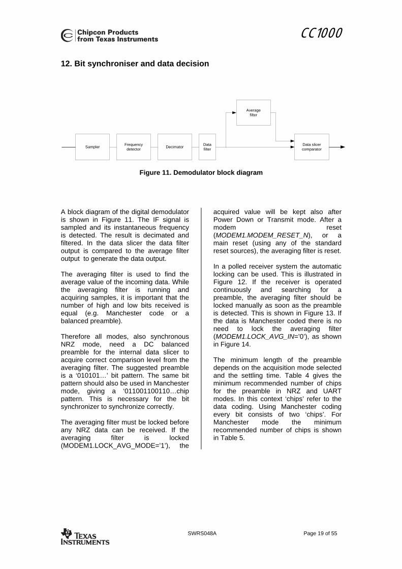
12. Bit synchroniser and data decision
Sampler
Averagefilter
DatafilterDecimatorFrequency
detectorData slicercomparator
Figure 11. Demodulator block diagram
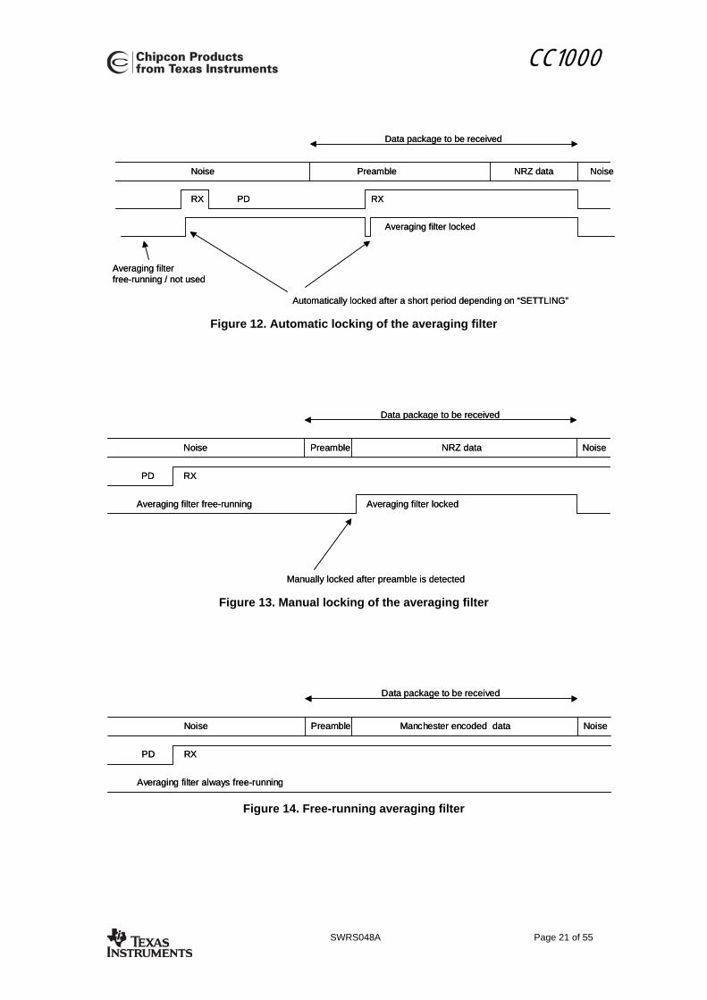
A block diagram of the digital demodulator is shown in Figure 11. The IF signal is sampled and its instantaneous frequency is detected. The result is decimated and filtered. In the data slicer the data filter output is compared to the average filter output to generate the data output. The averaging filter is used to find the average value of the incoming data. While the averaging filter is running and acquiring samples, it is important that the number of high and low bits received is equal (e.g. Manchester code or a balanced preamble). Therefore all modes, also synchronous NRZ mode, need a DC balanced preamble for the internal data slicer to acquire correct comparison level from the averaging filter. The suggested preamble is a ‘010101…’ bit pattern. The same bit pattern should also be used in Manchester mode, giving a ‘011001100110…chip pattern. This is necessary for the bit synchronizer to synchronize correctly. The averaging filter must be locked before any NRZ data can be received. If the averaging filter is locked (MODEM1.LOCK_AVG_MODE=’1’), the
acquired value will be kept also after Power Down or Transmit mode. After a modem reset (MODEM1.MODEM_RESET_N), or a main reset (using any of the standard reset sources), the averaging filter is reset. In a polled receiver system the automatic locking can be used. This is illustrated in Figure 12. If the receiver is operated continuously and searching for a preamble, the averaging filter should be locked manually as soon as the preamble is detected. This is shown in Figure 13. If the data is Manchester coded there is no need to lock the averaging filter (MODEM1.LOCK_AVG_IN=’0’), as shown in Figure 14. The minimum length of the preamble depends on the acquisition mode selected and the settling time. Table 4 gives the minimum recommended number of chips for the preamble in NRZ and UART modes. In this context ‘chips’ refer to the data coding. Using Manchester coding every bit consists of two ‘chips’. For Manchester mode the minimum recommended number of chips is shown in Table 5.
CC1000
SWRS048A Page 20 of 55
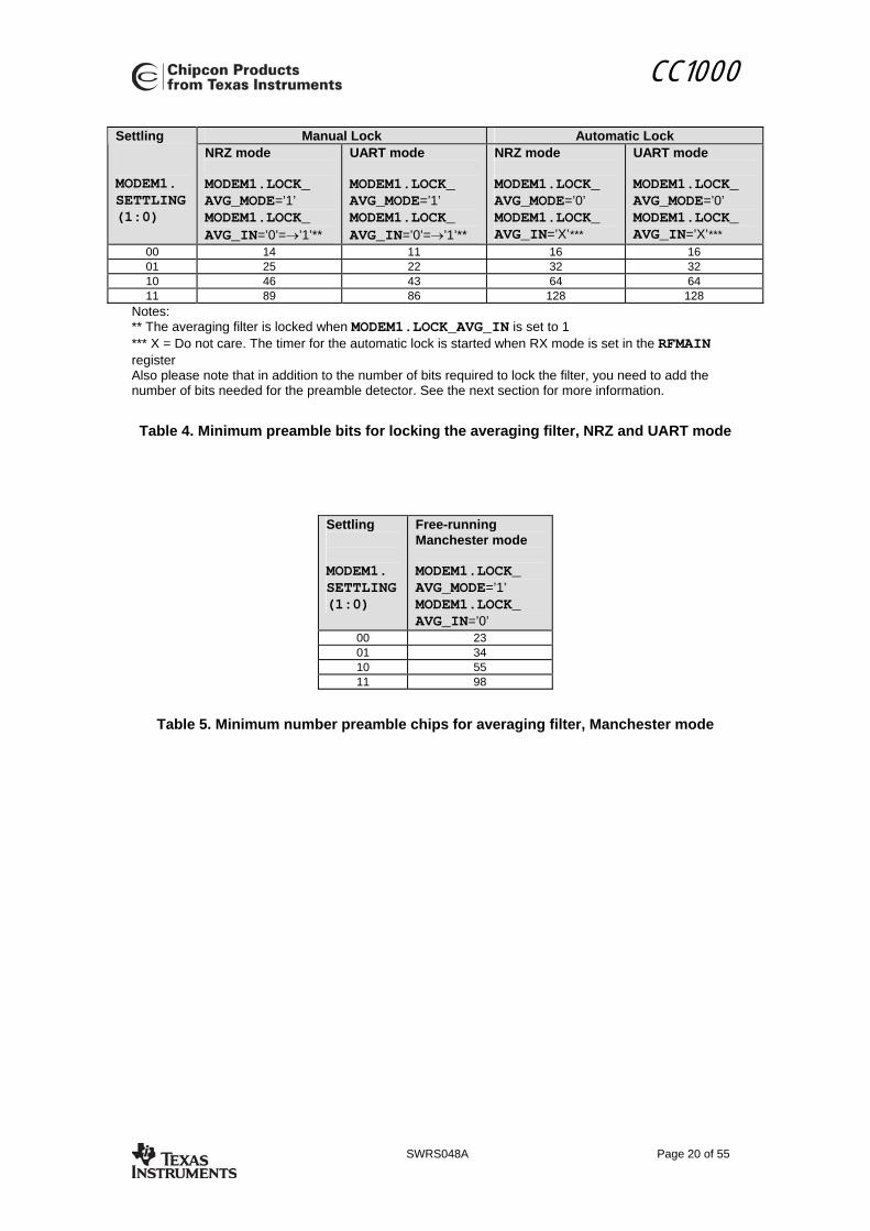
Manual Lock Automatic Lock Settling MODEM1. SETTLING(1:0)
NRZ mode MODEM1.LOCK_ AVG_MODE=’1’ MODEM1.LOCK_ AVG_IN=’0’=→’1’**
UART mode MODEM1.LOCK_ AVG_MODE=’1’ MODEM1.LOCK_ AVG_IN=’0’=→’1’**
NRZ mode MODEM1.LOCK_ AVG_MODE=’0’ MODEM1.LOCK_ AVG_IN=’X’***
UART mode MODEM1.LOCK_ AVG_MODE=’0’ MODEM1.LOCK_ AVG_IN=’X’***
00 14 11 16 16 01 25 22 32 32 10 46 43 64 64 11 89 86 128 128
Notes: ** The averaging filter is locked when MODEM1.LOCK_AVG_IN is set to 1 *** X = Do not care. The timer for the automatic lock is started when RX mode is set in the RFMAIN register Also please note that in addition to the number of bits required to lock the filter, you need to add the number of bits needed for the preamble detector. See the next section for more information.
Table 4. Minimum preamble bits for locking the averaging filter, NRZ and UART mode
Settling MODEM1. SETTLING(1:0)
Free-running Manchester mode MODEM1.LOCK_ AVG_MODE=’1’ MODEM1.LOCK_ AVG_IN=’0’
00 23 01 34 10 55 11 98
Table 5. Minimum number preamble chips for averaging filter, Manchester mode
CC1000
SWRS048A Page 21 of 55
Preamble NRZ data
Data package to be received
RX
Noise
RXPD
Averaging filter free-running / not used
Automatically locked after a short period depending on “SETTLING”
Noise
Averaging filter locked
Preamble NRZ data
Data package to be received
RX
Noise
RXPD
Averaging filter free-running / not used
Automatically locked after a short period depending on “SETTLING”
Noise
Averaging filter locked
Figure 12. Automatic locking of the averaging filter
Preamble NRZ data
Data package to be received
RX
Noise
PD
Averaging filter free-running
Manually locked after preamble is detected
Noise
Averaging filter locked
Preamble NRZ data
Data package to be received
RX
Noise
PD
Averaging filter free-running
Manually locked after preamble is detected
Noise
Averaging filter locked
Figure 13. Manual locking of the averaging filter
Preamble Manchester encoded data
Data package to be received
RX
Noise
PD
Averaging filter always free-running
NoisePreamble Manchester encoded data
Data package to be received
RX
Noise
PD
Averaging filter always free-running
Noise
Figure 14. Free-running averaging filter
CC1000
SWRS048A Page 22 of 55
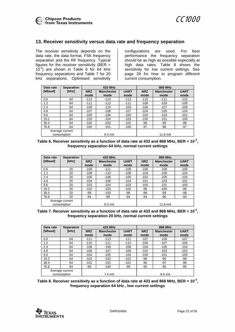
13. Receiver sensitivity versus data rate and frequency separation The receiver sensitivity depends on the data rate, the data format, FSK frequency separation and the RF frequency. Typical figures for the receiver sensitivity (BER = 10-3) are shown in Table 6 for 64 kHz frequency separations and Table 7 for 20 kHz separations. Optimised sensitivity
configurations are used. For best performance the frequency separation should be as high as possible especially at high data rates. Table 8 shows the sensitivity for low current settings. See page 28 for how to program different current consumption.
433 MHz 868 MHz Data rate
[kBaud] Separation
[kHz] NRZ mode
Manchester mode
UART mode
NRZ mode
Manchester mode
UART mode
0.6 64 -113 -114 -113 -110 -111 -110 1.2 64 -111 -112 -111 -108 -109 -108 2.4 64 -109 -110 -109 -106 -107 -106 4.8 64 -107 -108 -107 -104 -105 -104 9.6 64 -105 -106 -105 -102 -103 -102 19.2 64 -103 -104 -103 -100 -101 -100 38.4 64 -102 -103 -102 -98 -99 -98 76.8 64 -100 -101 -100 -97 -98 -97
Average current consumption
9.3 mA
11.8 mA
Table 6. Receiver sensitivity as a function of data rate at 433 and 868 MHz, BER = 10-3, frequency separation 64 kHz, normal current settings
433 MHz 868 MHz Data rate
[kBaud] Separation
[kHz] NRZ mode
Manchester mode
UART mode
NRZ mode
Manchester mode
UART mode
0.6 20 -109 -111 -109 -106 -108 -106 1.2 20 -108 -110 -108 -104 -106 -104 2.4 20 -106 -108 -106 -103 -105 -103 4.8 20 -104 -106 -104 -101 -103 -101 9.6 20 -103 -104 -103 -100 -101 -100 19.2 20 -102 -103 -102 -99 -100 -99 38.4 20 -98 -100 -98 -98 -99 -98 76.8 20 -94 -98 -94 -94 -96 -94
Average current consumption
9.3 mA
11.8 mA
Table 7. Receiver sensitivity as a function of data rate at 433 and 868 MHz, BER = 10-3, frequency separation 20 kHz, normal current settings
433 MHz 868 MHz Data rate
[kBaud] Separation
[kHz] NRZ mode
Manchester mode
UART mode
NRZ mode
Manchester mode
UART mode
0.6 64 -111 -113 -111 -107 -109 -107 1.2 64 -110 -111 -110 -106 -107 -106 2.4 64 -108 -109 -108 -104 -105 -104 4.8 64 -106 -107 -106 -102 -103 -102 9.6 64 -104 -105 -104 -100 -101 -100 19.2 64 -102 -103 -102 -98 -99 -98 38.4 64 -101 -102 -101 -96 -97 -96 76.8 64 -99 -100 -99 -95 -96 -95
Average current consumption
7.4 mA
9.6 mA
Table 8. Receiver sensitivity as a function of data rate at 433 and 868 MHz, BER = 10-3, frequency separation 64 kHz , low current settings
CC1000
SWRS048A Page 23 of 55
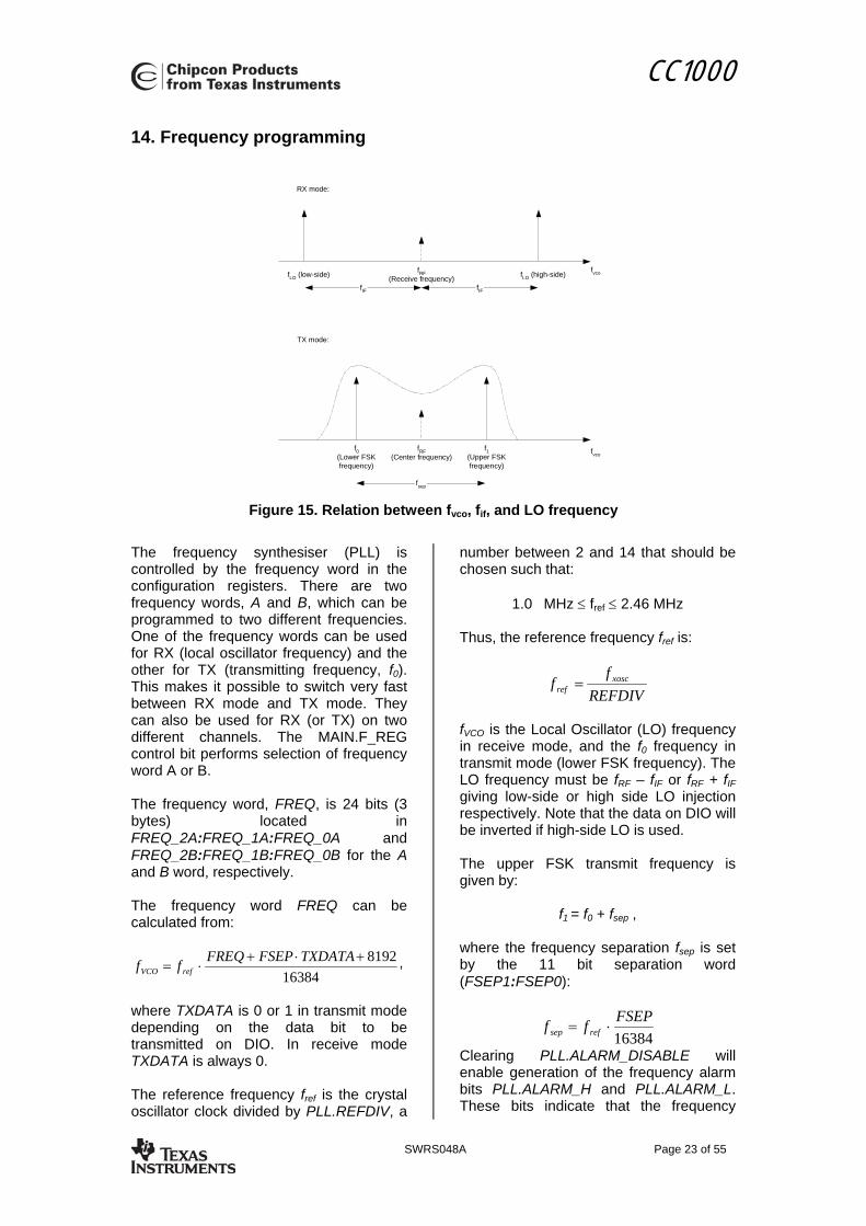
14. Frequency programming
RX mode:
fLO (low-side) fLO (high-side)fRF(Receive frequency)
fIF fIF
TX mode:
fRF(Center frequency)
fsep
f0(Lower FSKfrequency)
f1(Upper FSKfrequency)
fvco
fvco
Figure 15. Relation between fvco, fif, and LO frequency
The frequency synthesiser (PLL) is controlled by the frequency word in the configuration registers. There are two frequency words, A and B, which can be programmed to two different frequencies. One of the frequency words can be used for RX (local oscillator frequency) and the other for TX (transmitting frequency, f0). This makes it possible to switch very fast between RX mode and TX mode. They can also be used for RX (or TX) on two different channels. The MAIN.F_REG control bit performs selection of frequency word A or B. The frequency word, FREQ, is 24 bits (3 bytes) located in FREQ_2A:FREQ_1A:FREQ_0A and FREQ_2B:FREQ_1B:FREQ_0B for the A and B word, respectively. The frequency word FREQ can be calculated from:
163848192+⋅+
⋅=TXDATAFSEPFREQff refVCO
,
where TXDATA is 0 or 1 in transmit mode depending on the data bit to be transmitted on DIO. In receive mode TXDATA is always 0. The reference frequency fref is the crystal oscillator clock divided by PLL.REFDIV, a
number between 2 and 14 that should be chosen such that:
1.0 MHz ≤ fref ≤ 2.46 MHz Thus, the reference frequency fref is:
REFDIVf
f xoscref =
fVCO is the Local Oscillator (LO) frequency in receive mode, and the f0 frequency in transmit mode (lower FSK frequency). The LO frequency must be fRF – fIF or fRF + fIF giving low-side or high side LO injection respectively. Note that the data on DIO will be inverted if high-side LO is used. The upper FSK transmit frequency is given by:
f1 = f0 + fsep , where the frequency separation fsep is set by the 11 bit separation word (FSEP1:FSEP0):
16384FSEPff refsep ⋅=
Clearing PLL.ALARM_DISABLE will enable generation of the frequency alarm bits PLL.ALARM_H and PLL.ALARM_L. These bits indicate that the frequency
CC1000
SWRS048A Page 24 of 55
synthesis PLL is near the limit of generate the frequency requested, and the PLL should be recalibrated. It is recommended that the LOCK_CONTINOUS bit in the LOCK
register is checked when changing frequencies and when changing between RX and TX mode. If lock is not achieved, a calibration should be performed.
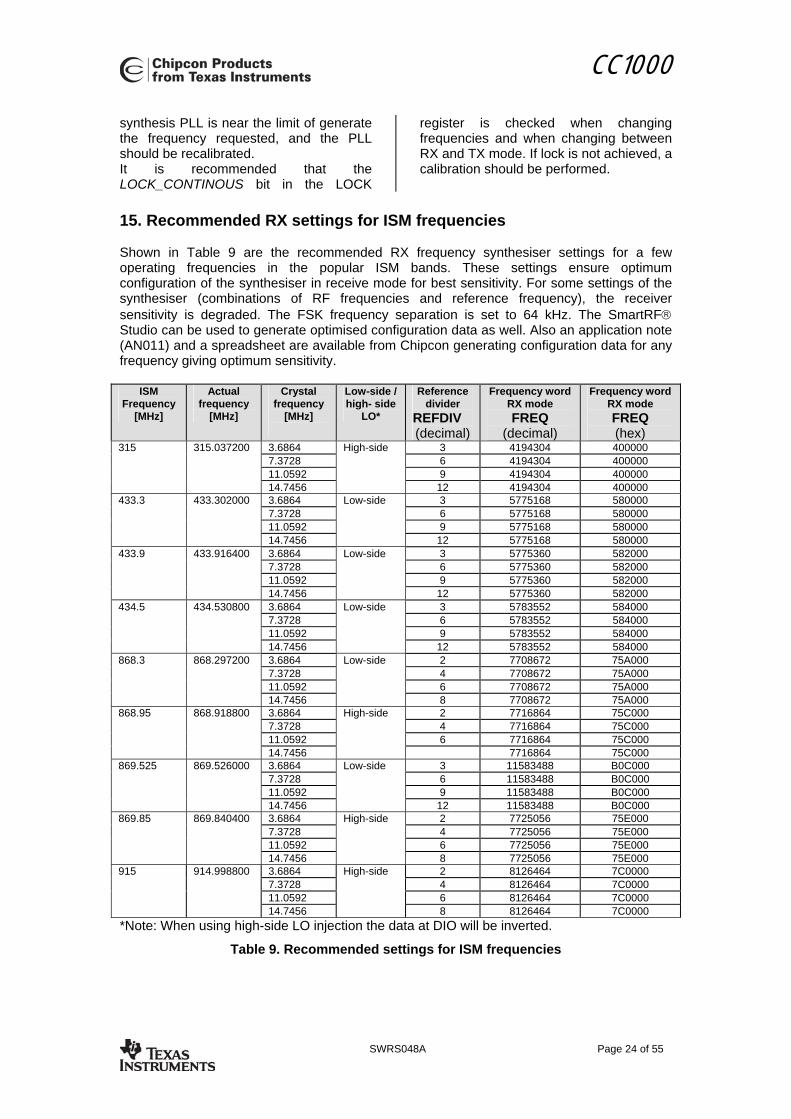
15. Recommended RX settings for ISM frequencies Shown in Table 9 are the recommended RX frequency synthesiser settings for a few operating frequencies in the popular ISM bands. These settings ensure optimum configuration of the synthesiser in receive mode for best sensitivity. For some settings of the synthesiser (combinations of RF frequencies and reference frequency), the receiver sensitivity is degraded. The FSK frequency separation is set to 64 kHz. The SmartRF® Studio can be used to generate optimised configuration data as well. Also an application note (AN011) and a spreadsheet are available from Chipcon generating configuration data for any frequency giving optimum sensitivity.
ISM
Frequency [MHz]
Actual frequency
[MHz]
Crystal frequency
[MHz]
Low-side / high- side
LO*
Reference divider
REFDIV (decimal)
Frequency word RX mode FREQ
(decimal)
Frequency word RX mode FREQ (hex)
315 315.037200 3.6864 High-side 3 4194304 400000 7.3728 6 4194304 400000 11.0592 9 4194304 400000 14.7456 12 4194304 400000 433.3 433.302000 3.6864 Low-side 3 5775168 580000 7.3728 6 5775168 580000 11.0592 9 5775168 580000 14.7456 12 5775168 580000 433.9 433.916400 3.6864 Low-side 3 5775360 582000 7.3728 6 5775360 582000 11.0592 9 5775360 582000 14.7456 12 5775360 582000 434.5 434.530800 3.6864 Low-side 3 5783552 584000 7.3728 6 5783552 584000 11.0592 9 5783552 584000 14.7456 12 5783552 584000 868.3 868.297200 3.6864 Low-side 2 7708672 75A000 7.3728 4 7708672 75A000 11.0592 6 7708672 75A000 14.7456 8 7708672 75A000 868.95 868.918800 3.6864 High-side 2 7716864 75C000 7.3728 4 7716864 75C000 11.0592 6 7716864 75C000 14.7456 7716864 75C000 869.525 869.526000 3.6864 Low-side 3 11583488 B0C000 7.3728 6 11583488 B0C000 11.0592 9 11583488 B0C000 14.7456 12 11583488 B0C000 869.85 869.840400 3.6864 High-side 2 7725056 75E000 7.3728 4 7725056 75E000 11.0592 6 7725056 75E000 14.7456 8 7725056 75E000 915 914.998800 3.6864 High-side 2 8126464 7C0000 7.3728 4 8126464 7C0000 11.0592 6 8126464 7C0000 14.7456 8 8126464 7C0000 *Note: When using high-side LO injection the data at DIO will be inverted.
Table 9. Recommended settings for ISM frequencies

CC1000
SWRS048A Page 25 of 55
16. VCO Only one external inductor (L101) is required for the VCO. The inductor will determine the operating frequency range of the circuit. It is important to place the inductor as close to the pins as possible in order to reduce stray inductance. It is recommended to use a high Q, low tolerance inductor for best performance.
Typical tuning range for the integrated varactor is 20-25%. Component values for various frequencies are given in Table 1. Component values for other frequencies can be found using the SmartRF® Studio software.
17. VCO and PLL self-calibration To compensate for supply voltage, temperature and process variations the VCO and PLL must be calibrated. The calibration is done automatically and sets maximum VCO tuning range and optimum charge pump current for PLL stability. After setting up the device at the operating frequency, the self-calibration can be initiated by setting the CAL_START bit. The calibration result is stored internally in the chip, and is valid as long as power is not turned off. If large supply voltage variations (more than 0.5 V) or temperature variations (more than 40 degrees) occur after calibration, a new calibration should be performed. The self-calibration is controlled through the CAL register (see configuration registers description p. 39). The CAL_COMPLETE bit indicates complete calibration. The user can poll this bit, or simply wait for 34 ms (calibration wait time when CAL_WAIT = 1). The wait time is proportional to the internal PLL reference frequency. The lowest permitted reference frequency (1 MHz) gives 34 ms wait time, which is therefore the worst case.
Reference frequency [MHz]
Calibration time [ms]
2.4 14 2.0 17 1.5 23 1.0 34
The CAL_COMPLETE bit can also be monitored at the CHP_OUT (LOCK) pin (configured by LOCK_SELECT[3:0]) and used as an interrupt input to the microcontroller. The CAL_START bit must be set to 0 by the microcontroller after the calibration is done.
There are separate calibration values for the two frequency registers. If the two frequencies, A and B, differ more than 1 MHz, or different VCO currents are used (VCO_CURRENT[3:0] in the CURRENT register) the calibration should be done separately. When using a 10.7 MHz external IF the LO is 10.7 MHz below/above the transmit frequency, hence separate calibration must be done. The CAL_DUAL bit in the CAL register controls dual or separate calibration. The single calibration algorithm, using separate calibration for RX and TX frequency, is illustrated in Figure 16. In Figure 17 the dual calibration algorithm is shown for two RX frequencies. It could also be used for two TX frequencies, or even for one RX and one TX frequency if the same VCO current is used. In multi-channel and frequency hopping applications the PLL calibration values may be read and stored for later use. By reading back calibration values and frequency change can be done without doing a re-calibration which could take up to 34 ms. The calibration value is stored in the TEST0 and TEST2 registers after a calibration is completed. Note that when using single calibration, calibration values are stored separately for frequency registers A and B. This means that the TEST0 and TEST2 registers will contain calibration settings for the currently selected frequency register (selected by F_REG in the MAIN register). The calibration value can later be written into TEST5 and TEST 6 to bypass the calibration. Note that you must set VCO_OVERRIDE=1 in TEST5 and CHP_OVERRIDE=1 in the TEST6 register.

CC1000
SWRS048A Page 26 of 55
Write CAL:CAL_START=0
End of calibration
Wait for maximum 34 ms, or Read CAL and wait until CAL_COMPLETE=1
Start single calibration
RX frequency register A is calibrated firstWrite MAIN:RXTX = 0; F_REG = 0RX_PD = 0; TX_PD = 1; FS_PD = 0CORE_PD = 0; BIAS_PD = 0; RESET_N=1
Write FREQ_A, FREQ_BIf DR>=9.6kBd then write TEST4: L2KIO=3FhWrite CAL: CAL_DUAL = 0
Frequency register A is used for RX mode, register B for TX
Write CAL:CAL_START=1
Calibration is performed in RX mode,Result is stored in TEST0 and TEST2,RX register
Write CURRENT = RX currentWrite PLL = RX pll
Update CURRENT and PLL for RX mode
Write CAL:CAL_START=0
Wait for 34 ms, or Read CAL and wait until CAL_COMPLETE=1
TX frequency register B is calibrated secondWrite MAIN:RXTX = 1; F_REG = 1RX_PD = 1; TX_PD = 0; FS_PD = 0CORE_PD = 0; BIAS_PD = 0; RESET_N=1
Write CAL:CAL_START=1
Calibration is performed in TX mode,Result is stored in TEST0 and TEST2, TX registers
Write CURRENT = TX currentWrite PLL = TX pllWrite PA_POW = 00h
Update CURRENT and PLL for TX modePA is turned off to prevent spurious emission
Calibration time depend on the reference frequency, see text.
Write CAL:CAL_START=0
End of calibration
Wait for maximum 34 ms, or Read CAL and wait until CAL_COMPLETE=1
Start single calibration
RX frequency register A is calibrated firstWrite MAIN:RXTX = 0; F_REG = 0RX_PD = 0; TX_PD = 1; FS_PD = 0CORE_PD = 0; BIAS_PD = 0; RESET_N=1
Write FREQ_A, FREQ_BIf DR>=9.6kBd then write TEST4: L2KIO=3FhWrite CAL: CAL_DUAL = 0
Frequency register A is used for RX mode, register B for TX
Write CAL:CAL_START=1
Calibration is performed in RX mode,Result is stored in TEST0 and TEST2,RX register
Write CURRENT = RX currentWrite PLL = RX pll
Update CURRENT and PLL for RX mode
Write CAL:CAL_START=0
Wait for 34 ms, or Read CAL and wait until CAL_COMPLETE=1
TX frequency register B is calibrated secondWrite MAIN:RXTX = 1; F_REG = 1RX_PD = 1; TX_PD = 0; FS_PD = 0CORE_PD = 0; BIAS_PD = 0; RESET_N=1
Write CAL:CAL_START=1
Calibration is performed in TX mode,Result is stored in TEST0 and TEST2, TX registers
Write CURRENT = TX currentWrite PLL = TX pllWrite PA_POW = 00h
Update CURRENT and PLL for TX modePA is turned off to prevent spurious emission
Calibration time depend on the reference frequency, see text.
Figure 16. Single calibration algorithm for RX and TX
CC1000
SWRS048A Page 27 of 55
Write CAL:CAL_START=0
End of calibration
Wait for maximum 34 ms, or Read CAL and wait until CAL_COMPLETE=1
Start dual calibration
Either frequency register A or B is selectedWrite MAIN:RXTX = 0; F_REG = 0RX_PD = 0; TX_PD = 1; FS_PD = 0CORE_PD = 0; BIAS_PD = 0; RESET_N=1
Write FREQ_A, FREQ_BIf DR>=38kBd then write TEST4: L2KIO=3FhWrite CAL: CAL_DUAL = 1
Frequency registers A and B are both used for RX mode
Write CAL:CAL_START=1
Dual calibration is performed.Result is stored in TEST0 and TEST2,for both frequency A and B registers
Write CURRENT= RX currentWrite PLL= RX pll
Update CURRENT and PLL for RX mode
Calibration time depend on the reference frequency, see text.
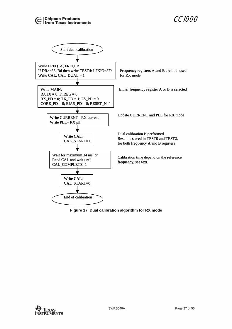
Figure 17. Dual calibration algorithm for RX mode

CC1000
SWRS048A Page 28 of 55
18. VCO and LNA current control The VCO current is programmable and should be set according to operating frequency RX/TX mode and output power. Recommended settings for the VCO_CURRENT bits in the CURRENT register are shown in the tables on page 41.
The bias current for the LNA, and the LO and PA buffers are also programmable. Table 10 shows the current consumption and receiver sensitivity for different settings (2.4 kBaud Manchester encoded data).
CURRENT register FRONT_END register RF freq-
uency [MHz]
Current consumption
[mA]
Sensitivity [dBm] VCO_
CURRENT [3:0]
LO_DRIVE [1:0]
PA_DRIVE [1:0]
BUF_CURRENT
LNA_CURRENT[1:0]
433 9.3 -110 0100 01 00 0 10 433 7.4 -109 0100 00 00 0 00 868 11.8 -107 1000 11 00 1 10 868 9.6 -105 1000 10 00 0 00 Note: Current consumption and sensitivity are typical figures at 2.4 kBaud Manchester encoded data, BER 10-3
Table 10. Receiver sensitivity as function of current consumption
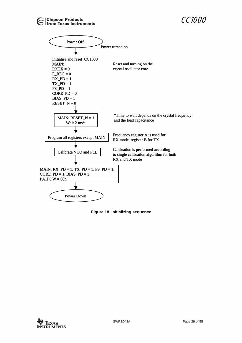
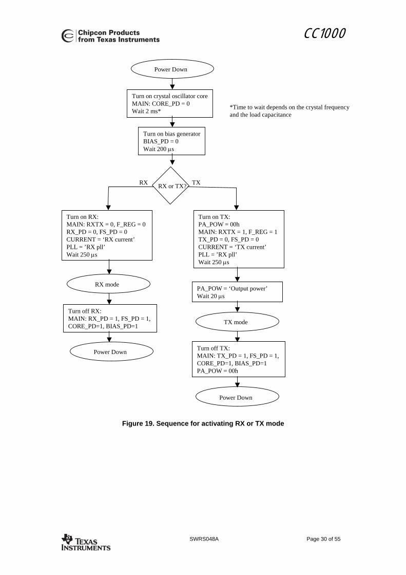
19. Power management CC1000 offers great flexibility for power management in order to meet strict power consumption requirements in battery operated applications. Power Down mode is controlled through the MAIN register. There are separate bits to control the RX part, the TX part, the frequency synthesiser and the crystal oscillator (see page 39). This individual control can be used to optimise for lowest possible current consumption in a certain application.
A typical power-on and initialising sequence for minimum power consumption is shown in Figure 18 and Figure 19. PALE should be tri-stated or set to a high level during power down mode in order to prevent a trickle current from flowing in the internal pull-up resistor. PA_POW should be set to 00h before power down mode to ensure lowest possible leakage current.
CC1000
SWRS048A Page 29 of 55
Figure 18. Initializing sequence
Power Down
Power OffPower turned on
Initialise and reset CC1000MAIN:RXTX = 0F_REG = 0RX_PD = 1TX_PD = 1FS_PD = 1CORE_PD = 0BIAS_PD = 1RESET_N = 0
Program all registers except MAIN Frequency register A is used for RX mode, register B for TX
Calibrate VCO and PLL Calibration is performed according to single calibration algorithm for bothRX and TX mode
MAIN: RESET_N = 1Wait 2 ms*
Reset and turning on the crystal oscillator core
*Time to wait depends on the crystal frequency and the load capacitance
MAIN: RX_PD = 1, TX_PD = 1, FS_PD = 1, CORE_PD = 1, BIAS_PD = 1PA_POW = 00h
CC1000
SWRS048A Page 30 of 55
Figure 19. Sequence for activating RX or TX mode
Turn on crystal oscillator coreMAIN: CORE_PD = 0Wait 2 ms*
Turn on bias generatorBIAS_PD = 0Wait 200 µs
Turn on RX: MAIN: RXTX = 0, F_REG = 0 RX_PD = 0, FS_PD = 0CURRENT = ‘RX current’PLL = ’RX pll’Wait 250 µs
RX or TX?
Power Down
*Time to wait depends on the crystal frequency and the load capacitance
RX mode
Turn off RX: MAIN: RX_PD = 1, FS_PD = 1, CORE_PD=1, BIAS_PD=1
Power Down
Turn on TX: PA_POW = 00hMAIN: RXTX = 1, F_REG = 1 TX_PD = 0, FS_PD = 0CURRENT = ‘TX current’PLL = ’RX pll’Wait 250 µs
TX mode
Turn off TX: MAIN: TX_PD = 1, FS_PD = 1, CORE_PD=1, BIAS_PD=1PA_POW = 00h
Power Down
PA_POW = ‘Output power’Wait 20 µs
RX TX
CC1000
SWRS048A Page 31 of 55
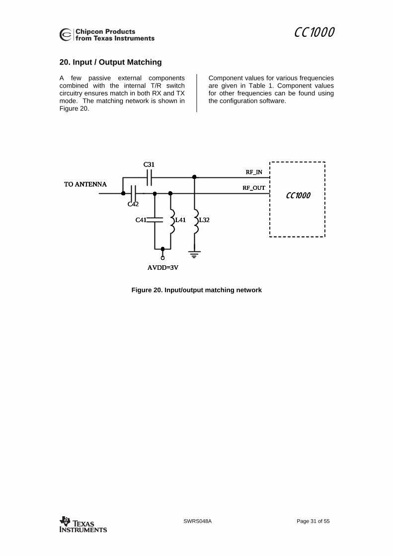
20. Input / Output Matching A few passive external components combined with the internal T/R switch circuitry ensures match in both RX and TX mode. The matching network is shown in Figure 20.
Component values for various frequencies are given in Table 1. Component values for other frequencies can be found using the configuration software.
Figure 20. Input/output matching network
RF_IN
RF_OUTTO ANTENNA
CC1000
L41C41
C42
AVDD=3V
L32
C31RF_IN
RF_OUTTO ANTENNA
CC1000
L41C41
C42
AVDD=3V
L32
C31RF_IN
RF_OUTTO ANTENNA
CC1000
L41C41
C42
AVDD=3V
L32
C31RF_IN
RF_OUTTO ANTENNA
CC1000
L41C41
C42
AVDD=3V
L32
C31
CC1000
SWRS048A Page 32 of 55
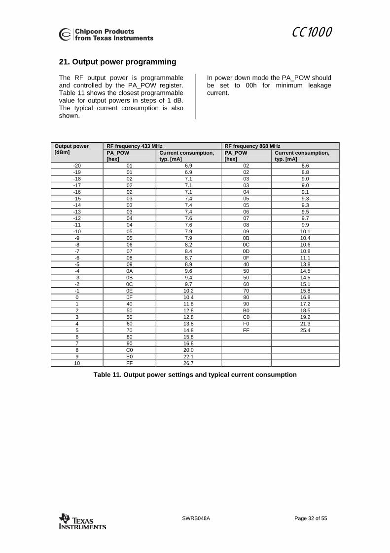
21. Output power programming
The RF output power is programmable and controlled by the PA_POW register. Table 11 shows the closest programmable value for output powers in steps of 1 dB. The typical current consumption is also shown.
In power down mode the PA_POW should be set to 00h for minimum leakage current.
RF frequency 433 MHz RF frequency 868 MHz Output power [dBm] PA_POW
[hex] Current consumption, typ. [mA]
PA_POW [hex]
Current consumption, typ. [mA]
-20 01 6.9 02 8.6 -19 01 6.9 02 8.8 -18 02 7.1 03 9.0 -17 02 7.1 03 9.0 -16 02 7.1 04 9.1 -15 03 7.4 05 9.3 -14 03 7.4 05 9.3 -13 03 7.4 06 9.5 -12 04 7.6 07 9.7 -11 04 7.6 08 9.9 -10 05 7.9 09 10.1 -9 05 7.9 0B 10.4 -8 06 8.2 0C 10.6 -7 07 8.4 0D 10.8 -6 08 8.7 0F 11.1 -5 09 8.9 40 13.8 -4 0A 9.6 50 14.5 -3 0B 9.4 50 14.5 -2 0C 9.7 60 15.1 -1 0E 10.2 70 15.8 0 0F 10.4 80 16.8 1 40 11.8 90 17.2 2 50 12.8 B0 18.5 3 50 12.8 C0 19.2 4 60 13.8 F0 21.3 5 70 14.8 FF 25.4 6 80 15.8 7 90 16.8 8 C0 20.0 9 E0 22.1
10 FF 26.7
Table 11. Output power settings and typical current consumption
CC1000
SWRS048A Page 33 of 55
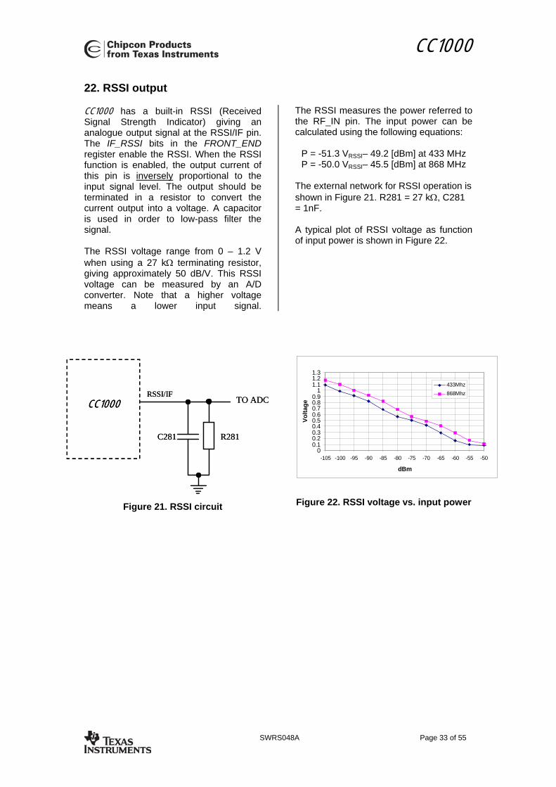
22. RSSI output CC1000 has a built-in RSSI (Received Signal Strength Indicator) giving an analogue output signal at the RSSI/IF pin. The IF_RSSI bits in the FRONT_END register enable the RSSI. When the RSSI function is enabled, the output current of this pin is inversely proportional to the input signal level. The output should be terminated in a resistor to convert the current output into a voltage. A capacitor is used in order to low-pass filter the signal. The RSSI voltage range from 0 – 1.2 V when using a 27 kΩ terminating resistor, giving approximately 50 dB/V. This RSSI voltage can be measured by an A/D converter. Note that a higher voltage means a lower input signal.
The RSSI measures the power referred to the RF_IN pin. The input power can be calculated using the following equations:
P = -51.3 VRSSI– 49.2 [dBm] at 433 MHz P = -50.0 VRSSI– 45.5 [dBm] at 868 MHz
The external network for RSSI operation is shown in Figure 21. R281 = 27 kΩ, C281 = 1nF. A typical plot of RSSI voltage as function of input power is shown in Figure 22.
Figure 21. RSSI circuit
00.10.20.30.40.50.60.70.80.9
11.11.21.3
-105 -100 -95 -90 -85 -80 -75 -70 -65 -60 -55 -50
dBm
Volta
ge
433Mhz868Mhz
Figure 22. RSSI voltage vs. input power
RSSI/IFTO ADCCC1000
R281C281
RSSI/IFTO ADCCC1000
R281C281
CC1000
SWRS048A Page 34 of 55
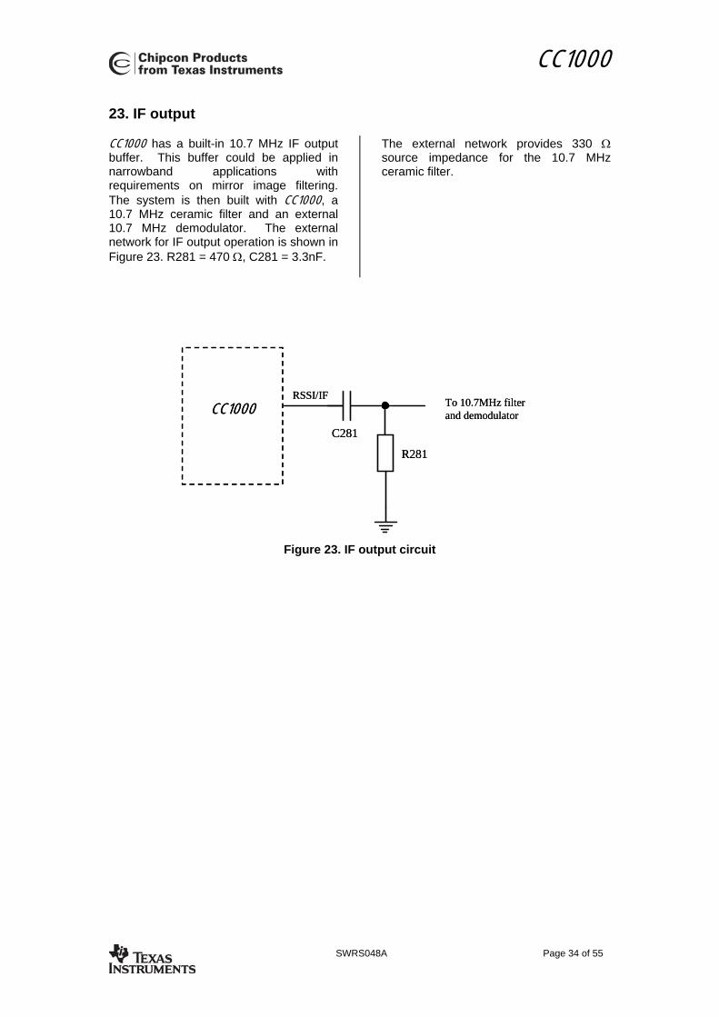
23. IF output CC1000 has a built-in 10.7 MHz IF output buffer. This buffer could be applied in narrowband applications with requirements on mirror image filtering. The system is then built with CC1000, a 10.7 MHz ceramic filter and an external 10.7 MHz demodulator. The external network for IF output operation is shown in Figure 23. R281 = 470 Ω, C281 = 3.3nF.
The external network provides 330 Ω source impedance for the 10.7 MHz ceramic filter.
RSSI/IFCC1000
R281
C281
To 10.7MHz filter and demodulator
RSSI/IFCC1000
R281
C281
To 10.7MHz filter and demodulator
Figure 23. IF output circuit
CC1000
SWRS048A Page 35 of 55
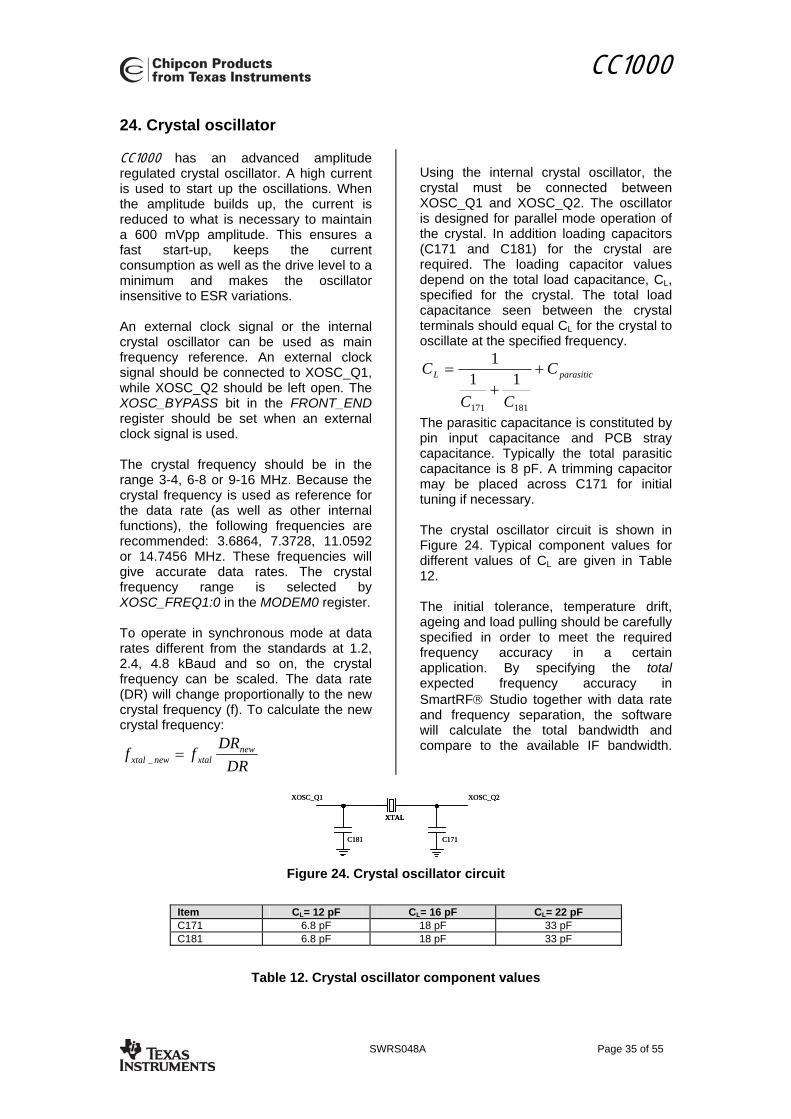
24. Crystal oscillator CC1000 has an advanced amplitude regulated crystal oscillator. A high current is used to start up the oscillations. When the amplitude builds up, the current is reduced to what is necessary to maintain a 600 mVpp amplitude. This ensures a fast start-up, keeps the current consumption as well as the drive level to a minimum and makes the oscillator insensitive to ESR variations. An external clock signal or the internal crystal oscillator can be used as main frequency reference. An external clock signal should be connected to XOSC_Q1, while XOSC_Q2 should be left open. The XOSC_BYPASS bit in the FRONT_END register should be set when an external clock signal is used. The crystal frequency should be in the range 3-4, 6-8 or 9-16 MHz. Because the crystal frequency is used as reference for the data rate (as well as other internal functions), the following frequencies are recommended: 3.6864, 7.3728, 11.0592 or 14.7456 MHz. These frequencies will give accurate data rates. The crystal frequency range is selected by XOSC_FREQ1:0 in the MODEM0 register. To operate in synchronous mode at data rates different from the standards at 1.2, 2.4, 4.8 kBaud and so on, the crystal frequency can be scaled. The data rate (DR) will change proportionally to the new crystal frequency (f). To calculate the new crystal frequency:
DRDR
ff newxtalnewxtal =_
Using the internal crystal oscillator, the crystal must be connected between XOSC_Q1 and XOSC_Q2. The oscillator is designed for parallel mode operation of the crystal. In addition loading capacitors (C171 and C181) for the crystal are required. The loading capacitor values depend on the total load capacitance, CL, specified for the crystal. The total load capacitance seen between the crystal terminals should equal CL for the crystal to oscillate at the specified frequency.
parasiticL C
CC
C ++
=
181171
111
The parasitic capacitance is constituted by pin input capacitance and PCB stray capacitance. Typically the total parasitic capacitance is 8 pF. A trimming capacitor may be placed across C171 for initial tuning if necessary. The crystal oscillator circuit is shown in Figure 24. Typical component values for different values of CL are given in Table 12. The initial tolerance, temperature drift, ageing and load pulling should be carefully specified in order to meet the required frequency accuracy in a certain application. By specifying the total expected frequency accuracy in SmartRF® Studio together with data rate and frequency separation, the software will calculate the total bandwidth and compare to the available IF bandwidth.
C171C181
XTAL
XOSC_Q1 XOSC_Q2
C171C181
XTALXTAL
XOSC_Q1 XOSC_Q2
Figure 24. Crystal oscillator circuit
Item CL= 12 pF CL= 16 pF CL= 22 pF C171 6.8 pF 18 pF 33 pF C181 6.8 pF 18 pF 33 pF
Table 12. Crystal oscillator component values
CC1000
SWRS048A Page 36 of 55
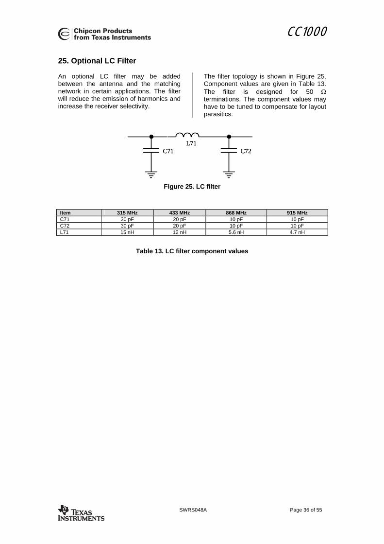
25. Optional LC Filter An optional LC filter may be added between the antenna and the matching network in certain applications. The filter will reduce the emission of harmonics and increase the receiver selectivity.
The filter topology is shown in Figure 25. Component values are given in Table 13. The filter is designed for 50 Ω terminations. The component values may have to be tuned to compensate for layout parasitics.
L71C71 C72
L71C71 C72
Figure 25. LC filter
Item 315 MHz 433 MHz 868 MHz 915 MHz C71 30 pF 20 pF 10 pF 10 pF C72 30 pF 20 pF 10 pF 10 pF L71 15 nH 12 nH 5.6 nH 4.7 nH
Table 13. LC filter component values

CC1000
SWRS048A Page 37 of 55
26. System Considerations and Guidelines 26.1 SRD regulations International regulations and national laws regulate the use of radio receivers and transmitters. SRDs (Short Range Devices) for licence free operation are allowed to operate in the 433 and 868-870 MHz bands in most European countries. In the United States such devices operate in the 260–470 and 902-928 MHz bands. CC1000 is designed to meet the requirements for operation in all these bands. A summary of the most important aspects of these regulations can be found in Application Note AN001 SRD regulations for licence free transceiver operation, available from Chipcon’s web site. 26.2 Low cost systems In systems where low cost is of great importance the CC1000 is the ideal choice. Very few external components keep the total cost at a minimum. The oscillator crystal can then be a low cost crystal with 50 ppm frequency tolerance. 26.3 Battery operated systems In low power applications the power down mode should be used when not being active. Depending on the start-up time requirement, the oscillator core can be powered during power down. See page 28 for information on how effective power management can be implemented. 26.4 Crystal drift compensation A unique feature in CC1000 is the very fine frequency resolution of 250 Hz. This can be used to do the temperature compensation of the crystal if the temperature drift curve is known and a temperature sensor is included in the system. Even initial adjustment can be done using the frequency programmability. This eliminates the need for an expensive
TCXO and trimming in some applications. In less demanding applications a crystal with low temperature drift and low ageing could be used without further compensation. A trimmer capacitor in the crystal oscillator circuit (in parallel with C171) could be used to set the initial frequency accurately. The fine frequency step programming cannot be used in RX mode if optimised frequency settings are required (see page 24). 26.5 High reliability systems Using a SAW filter as a preselector will improve the communication reliability in harsh environments by reducing the probability of blocking. The receiver sensitivity and the output power will be reduced due to the filter insertion loss. By inserting the filter in the RX path only, together with an external RX/TX switch, only the receiver sensitivity is reduced, and output power is remained. The CHP_OUT (LOCK) pin can be configured to control an external LNA, RX/TX switch or power amplifier. This is controlled by LOCK_SELECT in the LOCK register. 26.6 Frequency hopping spread spectrum systems Due to the very fast frequency shift properties of the PLL, the CC1000 is also suitable for frequency hopping systems. Hop rates of 1-100 hops/s are usually used depending on the bit rate and the amount of data to be sent during each transmission. The two frequency registers (FREQ_A and FREQ_B) are designed such that the ‘next’ frequency can be programmed while the ‘present’ frequency is used. The switching between the two frequencies is done through the MAIN register.
CC1000
SWRS048A Page 38 of 55
27. PCB Layout Recommendations Chipcon provide reference layouts that should be followed in order to achieve the best performance. The Chipcon reference design (CC1000PP and CC1000uCSP_EM) can be downloaded from the Chipcon website. A two layer PCB is highly recommended. The bottom layer of the PCB should be the “ground-layer”. The top layer should be used for signal routing, and the open areas should be filled with etallization connected to ground using several vias. The ground pins should be connected to ground as close as possible to the package pin using individual vias. The de-coupling capacitors should also be placed as close as possible to the supply pins and connected to the ground plane by separate vias. The external components should be as small as possible and surface mount
devices are required. The VCO inductor must be placed as close as possible to the chip and symmetrical with respect to the input pins. Precaution should be used when placing the microcontroller in order to avoid interference with the RF circuitry. In certain applications where the ground plane for the digital circuitry is expected to be noisy, the ground plane may be split in an analogue and a digital part. All AGND pins and AVDD de-coupling capacitors should be connected to the analogue ground plane. All DGND pins and DVDD de-coupling capacitors should be connected to the digital ground. The connection between the two ground planes should be implemented as a star connection with the power supply ground. A development kit with a fully assembled PCB is available, and can be used as a guideline for layout.
28. Antenna Considerations CC1000 can be used together with various types of antennas. The most common antennas for short range communication are monopole, helical and loop antennas. Monopole antennas are resonant antennas with a length corresponding to one quarter of the electrical wavelength (λ/4). They are very easy to design and can be implemented simply as a “piece of wire” or even integrated into the PCB. Non-resonant monopole antennas shorter than λ/4 can also be used, but at the expense of range. In size and cost critical applications such an antenna may very well be integrated into the PCB. Helical antennas can be thought of as a combination of a monopole and a loop antenna. They are a good compromise in size critical applications. But helical antennas tend to be more difficult to optimise than the simple monopole. Loop antennas are easy to integrate into the PCB, but are less effective due to
difficult impedance matching because of their very low radiation resistance. For low power applications the λ/4-monopole antenna is recommended giving the best range and because of its simplicity. The length of the λ/4-monopole antenna is given by:
L = 7125 / f
where f is in MHz, giving the length in cm. An antenna for 869 MHz should be 8.2 cm, and 16.4 cm for 434 MHz. The antenna should be connected as close as possible to the IC. If the antenna is located away from the input pin the antenna should be matched to the feeding transmission line (50 Ω). For a more thorough primer on antennas, please refer to Application Note AN003 SRD Antennas available from Chipcon’s web site.
CC1000
SWRS048A Page 39 of 55
29. Configuration registers The configuration of CC1000 is done by programming 22 8-bit configuration registers. The configuration data based on selected system parameters are most easily found by using the SmartRF®
Studio software. A complete description of the registers are given in the following tables. After a RESET is programmed all the registers have default values.
REGISTER OVERVIEW ADDRESS Byte Name Description
00h MAIN MAIN Register 01h FREQ_2A Frequency Register 2A 02h FREQ_1A Frequency Register 1A 03h FREQ_0A Frequency Register 0A 04h FREQ_2B Frequency Register 2B 05h FREQ_1B Frequency Register 1B 06h FREQ_0B Frequency Register 0B 07h FSEP1 Frequency Separation Register 1 08h FSEP0 Frequency Separation Register 0 09h CURRENT Current Consumption Control Register 0Ah FRONT_END Front End Control Register 0Bh PA_POW PA Output Power Control Register 0Ch PLL PLL Control Register 0Dh LOCK LOCK Status Register and signal select to CHP_OUT (LOCK) pin 0Eh CAL VCO Calibration Control and Status Register 0Fh MODEM2 Modem Control Register 2 10h MODEM1 Modem Control Register 1 11h MODEM0 Modem Control Register 0 12h MATCH Match Capacitor Array Control Register for RX and TX impedance matching 13h FSCTRL Frequency Synthesiser Control Register 14h Reserved 15h Reserved 16h Reserved 17h Reserved 18h Reserved 19h Reserved 1Ah Reserved 1Bh Reserved 1Ch PRESCALER Prescaler and IF-strip test control register 40h TEST6 Test register for PLL LOOP 41h TEST5 Test register for PLL LOOP 42h TEST4 Test register for PLL LOOP (must be updated as specified) 43h TEST3 Test register for VCO 44h TEST2 Test register for Calibration 45h TEST1 Test register for Calibration 46h TEST0 Test register for Calibration
CC1000
SWRS048A Page 40 of 55
MAIN Register (00h) REGISTER NAME Default
value Active Description
MAIN[7] RXTX - - RX/TX switch, 0 : RX , 1 : TX MAIN[6] F_REG - - Selection of Frequency Register, 0 : Register A, 1 :
Register B MAIN[5] RX_PD - H Power Down of LNA, Mixer, IF, Demodulator, RX part of
Signal Interface MAIN[4] TX_PD - H Power Down of TX part of Signal Interface, PA MAIN[3] FS_PD - H Power Down of Frequency Synthesiser MAIN[2] CORE_PD - H Power Down of Crystal Oscillator Core MAIN[1] BIAS_PD - H Power Down of BIAS (Global_Current_Generator)
and Crystal Oscillator Buffer MAIN[0] RESET_N - L Reset, active low. Writing RESET_N low will write default
values to all other registers than MAIN. Bits in MAIN do not have a default value, and will be written directly through the configurations interface. Must be set high to complete reset.
FREQ_2A Register (01h)
REGISTER NAME Default value
Active Description
FREQ_2A[7:0] FREQ_A[23:16] 01110101 - 8 MSB of frequency control word A FREQ_1A Register (02h)
REGISTER NAME Default value
Active Description
FREQ_1A[7:0] FREQ_A[15:8] 10100000 - Bit 15 to 8 of frequency control word A FREQ_0A Register (03h)
REGISTER NAME Default value
Active Description
FREQ_0A[7:0] FREQ_A[7:0] 11001011 - 8 LSB of frequency control word A FREQ_2B Register (04h)
REGISTER NAME Default value
Active Description
FREQ_2B[7:0] FREQ_B[23:16] 01110101 - 8 MSB of frequency control word B FREQ_1B Register (05h)
REGISTER NAME Default value
Active Description
FREQ_1B[7:0] FREQ_B[15:8] 10100101 - Bit 15 to 8 of frequency control word B FREQ_0B Register (06h)
REGISTER NAME Default value
Active Description
FREQ_0B[7:0] FREQ_B[7:0] 01001110 - 8 LSB of frequency control word B FSEP1 Register (07h)
REGISTER NAME Default value
Active Description
FSEP1[7:3] - - - Not used FSEP1[2:0] FSEP_MSB[2:0] 000 - 3 MSB of frequency separation control
FSEP0 Register (08h)
REGISTER NAME Default value
Active Description
FSEP0[7:0] FSEP_LSB[7:0] 01011001 - 8 LSB of frequency separation control
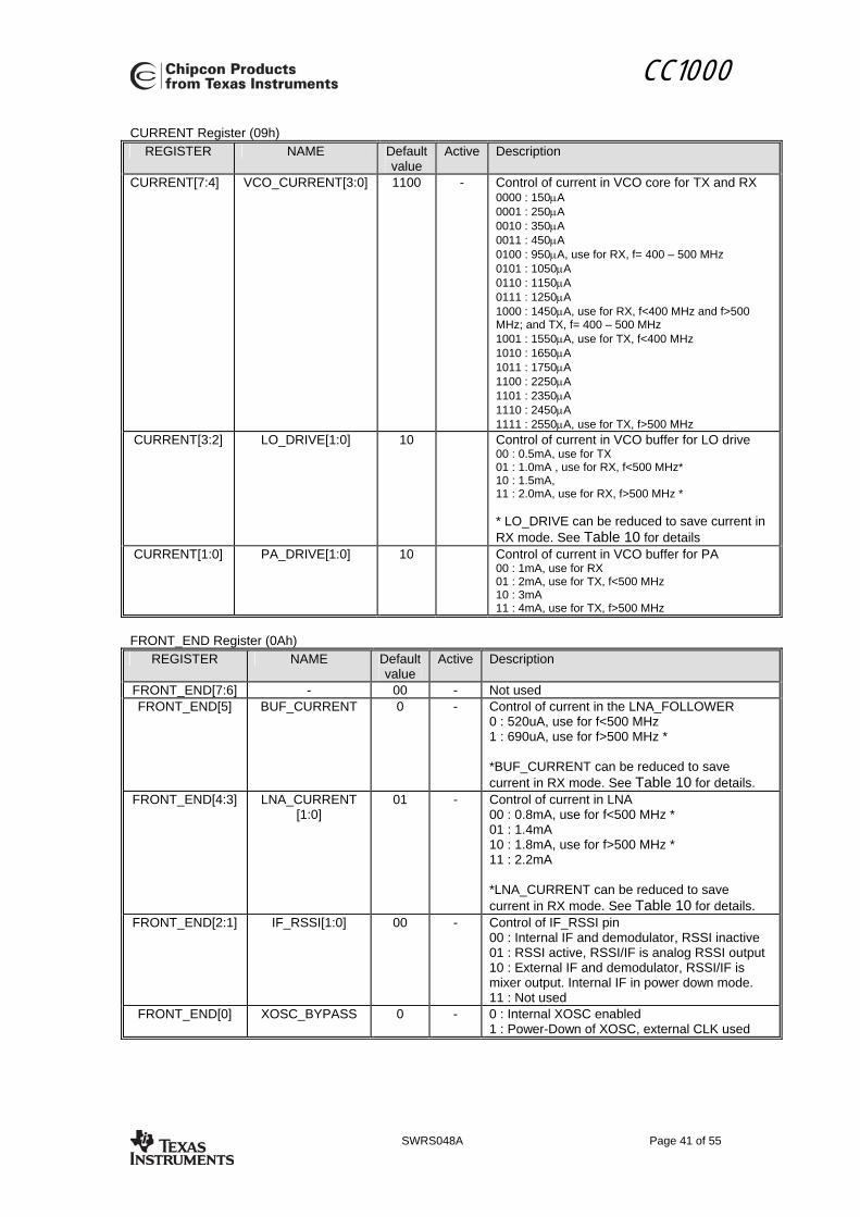
CC1000
SWRS048A Page 41 of 55
CURRENT Register (09h) REGISTER NAME Default
value Active Description
CURRENT[7:4] VCO_CURRENT[3:0] 1100 - Control of current in VCO core for TX and RX 0000 : 150µA 0001 : 250µA 0010 : 350µA 0011 : 450µA 0100 : 950µA, use for RX, f= 400 – 500 MHz 0101 : 1050µA 0110 : 1150µA 0111 : 1250µA 1000 : 1450µA, use for RX, f<400 MHz and f>500 MHz; and TX, f= 400 – 500 MHz 1001 : 1550µA, use for TX, f<400 MHz 1010 : 1650µA 1011 : 1750µA 1100 : 2250µA 1101 : 2350µA 1110 : 2450µA 1111 : 2550µA, use for TX, f>500 MHz
CURRENT[3:2] LO_DRIVE[1:0] 10 Control of current in VCO buffer for LO drive 00 : 0.5mA, use for TX 01 : 1.0mA , use for RX, f<500 MHz* 10 : 1.5mA, 11 : 2.0mA, use for RX, f>500 MHz * * LO_DRIVE can be reduced to save current in RX mode. See Table 10 for details
CURRENT[1:0] PA_DRIVE[1:0] 10 Control of current in VCO buffer for PA 00 : 1mA, use for RX 01 : 2mA, use for TX, f<500 MHz 10 : 3mA 11 : 4mA, use for TX, f>500 MHz
FRONT_END Register (0Ah)
REGISTER NAME Default value
Active Description
FRONT_END[7:6] - 00 - Not used FRONT_END[5] BUF_CURRENT 0 - Control of current in the LNA_FOLLOWER
0 : 520uA, use for f<500 MHz 1 : 690uA, use for f>500 MHz * *BUF_CURRENT can be reduced to save current in RX mode. See Table 10 for details.
FRONT_END[4:3] LNA_CURRENT [1:0]
01 - Control of current in LNA 00 : 0.8mA, use for f<500 MHz * 01 : 1.4mA 10 : 1.8mA, use for f>500 MHz * 11 : 2.2mA *LNA_CURRENT can be reduced to save current in RX mode. See Table 10 for details.
FRONT_END[2:1] IF_RSSI[1:0] 00 - Control of IF_RSSI pin 00 : Internal IF and demodulator, RSSI inactive 01 : RSSI active, RSSI/IF is analog RSSI output 10 : External IF and demodulator, RSSI/IF is mixer output. Internal IF in power down mode. 11 : Not used
FRONT_END[0] XOSC_BYPASS 0 - 0 : Internal XOSC enabled 1 : Power-Down of XOSC, external CLK used

CC1000
SWRS048A Page 42 of 55
PA_POW Register (0Bh) REGISTER NAME Default
value Active Description
PA_POW[7:4] PA_HIGHPOWER[3:0] 0000 - Control of output power in high power array. Should be 0000 in PD mode . See Table 11 page 32 for details.
PA_POW[3:0] PA_LOWPOWER[3:0] 1111 - Control of output power in low power array Should be 0000 in PD mode. See Table 11 page 32 for details.
PLL Register (0Ch)
REGISTER NAME Default value
Active Description
PLL[7] EXT_FILTER 0 - 1 : External loop filter 0 : Internal loop filter 1-to-0 transition samples F_COMP comparator when BREAK_LOOP=1 (TEST3)
PLL[6:3] REFDIV[3:0] 0010 - Reference divider 0000 : Not allowed 0001 : Not allowed 0010 : Divide by 2 0011 : Divide by 3 …........ 1111 : Divide by 15
PLL[2] ALARM_DISABLE 0 h 0 : Alarm function enabled 1 : Alarm function disabled
PLL[1] ALARM_H - - Status bit for tuning voltage out of range (too close to VDD)
PLL[0] ALARM_L - - Status bit for tuning voltage out of range (too close to GND)

CC1000
SWRS048A Page 43 of 55
LOCK Register (0Dh) REGISTE
R NAME Default
value Active Description
LOCK[7:4] LOCK_SELECT[3:0] 0000 - Selection of signals to CHP_OUT (LOCK) pin 0000 : Normal, pin can be used as CHP_OUT 0001 : LOCK_CONTINUOUS (active high) 0010 : LOCK_INSTANT (active high) 0011 : ALARM_H (active high) 0100 : ALARM_L (active high) 0101 : CAL_COMPLETE (active high) 0110 : IF_OUT 0111 : REFERENCE_DIVIDER Output 1000 : TX_PDB (active high, activates external PA when TX_PD=0) 1001 : Manchester Violation (active high) 1010 : RX_PDB (active high, activates external LNA when RX_PD=0) 1011 : Not defined 1100 : Not defined 1101 : LOCK_AVG_FILTER 1110 : N_DIVIDER Output 1111 : F_COMP
LOCK[3] PLL_LOCK_ ACCURACY
0 - 0 : Sets Lock Threshold = 127, Reset Lock Threshold = 111. Corresponds to a worst case accuracy of 0.7% 1 : Sets Lock Threshold = 31, Reset Lock Threshold =15. Corresponds to a worst case accuracy of 2.8%
LOCK[2] PLL_LOCK_ LENGTH
0 - 0 : Normal PLL lock window 1 : Not used
LOCK[1] LOCK_INSTANT - - Status bit from Lock Detector LOCK[0] LOCK_CONTINUOUS - - Status bit from Lock Detector
CAL Register (0Eh)
REGISTER NAME Default value
Active Description
CAL[7] CAL_START 0 ↑ ↑ 1 : Calibration started 0 : Calibration inactive CAL_START must be set to 0 after calibration is done
CAL[6] CAL_DUAL 0 H 1 : Store calibration in both A and B 0 : Store calibration in A or B defined by MAIN[6]
CAL[5] CAL_WAIT 0 H 1 : Normal Calibration Wait Time 0 : Half Calibration Wait Time The calibration time is proportional to the internal reference frequency. 2 MHz reference frequency gives 14 ms wait time.
CAL[4] CAL_CURRENT 0 H 1 : Calibration Current Doubled 0 : Normal Calibration Current
CAL[3] CAL_COMPLETE 0 H Status bit defining that calibration is complete
CAL[2:0] CAL_ITERATE 101 H Iteration start value for calibration DAC 000 – 101: Not used 110 : Normal start value 111 : Not used

CC1000
SWRS048A Page 44 of 55
MODEM2 Register (0Fh) REGISTER NAME Default
value Active Description
MODEM2[7] PEAKDETECT 1 H Peak Detector and Remover disabled or enabled 0 : Peak detector and remover is disabled 1 : Peak detector and remover is enabled
MODEM2[6:0] PEAK_LEVEL_OFFSET[6:0] 0010110 - Threshold level for Peak Remover in Demodulator. Correlated to frequency deviation, see note.
Note: PEAK_LEVEL_OFFSET[6:0] =
85
2⋅
∆+− fIF
FsIFFs
lowlow
where 1_
_+
=FREQXOSCxoscfFs
and accuracyXTALrffkHzIFlow __2150 ••−= and ∆f is the separation MODEM1 Register (10h)
REGISTER NAME Default value
Active Description
MODEM1[7:5] MLIMIT 011 - Sets the limit for the Manchester Violation Flag. A Manchester Value = 14 is a perfect bit and a Manchester Value = 0 is a constant level (an unbalanced corrupted bit) 000 : No Violation Flag is set 001 : Violation Flag is set for Manchester Value < 1 010 : Violation Flag is set for Manchester Value < 2 011 : Violation Flag is set for Manchester Value < 3 100 : Violation Flag is set for Manchester Value < 4 101 : Violation Flag is set for Manchester Value < 5 110 : Violation Flag is set for Manchester Value < 6 111 : Violation Flag is set for Manchester Value < 7
MODEM1[4] LOCK_AVG_IN 0 H Lock control bit of Average Filter 0 : Average Filter is free-running 1 : Average Filter is locked
MODEM1[3] LOCK_AVG_MODE 0 - Automatic lock of Average Filter 0 : Lock of Average Filter is controlled automatically1 : Lock of Average Filter is controlled by LOCK_AVG_IN
MODEM1[2:1] SETTLING[1:0] 11 - Settling Time of Average Filter 00 : 11 baud settling time, worst case 1.2dB loss in sensitivity 01 : 22 baud settling time, worst case 0.6dB loss in sensitivity 10 : 43 baud settling time, worst case 0.3dB loss in sensitivity 11 : 86 baud settling time, worst case 0.15dB loss in sensitivity
MODEM1[0] MODEM_RESET_N 1 L Separate reset of MODEM
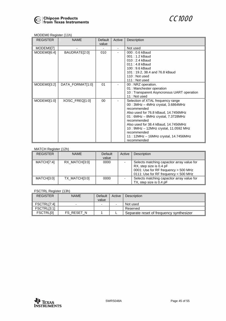
CC1000
SWRS048A Page 45 of 55
MODEM0 Register (11h) REGISTER NAME Default
value Active Description
MODEM0[7] - - - Not used MODEM0[6:4] BAUDRATE[2:0] 010 - 000 : 0.6 kBaud
001 : 1.2 kBaud 010 : 2.4 kBaud 011 : 4.8 kBaud 100 : 9.6 kBaud 101 : 19.2, 38.4 and 76.8 kBaud 110 : Not used 111 : Not used
MODEM0[3:2] DATA_FORMAT[1:0] 01 - 00 : NRZ operation. 01 : Manchester operation 10 : Transparent Asyncronous UART operation 11 : Not used
MODEM0[1:0] XOSC_FREQ[1:0] 00 - Selection of XTAL frequency range 00 : 3MHz – 4MHz crystal, 3.6864MHz recommended Also used for 76.8 kBaud, 14.7456MHz 01 : 6MHz – 8MHz crystal, 7.3728MHz recommended Also used for 38.4 kBaud, 14.7456MHz 10 : 9MHz – 12MHz crystal, 11.0592 MHz recommended 11 : 12MHz – 16MHz crystal, 14.7456MHz recommended
MATCH Register (12h)
REGISTER NAME Default value
Active Description
MATCH[7:4] RX_MATCH[3:0] 0000 - Selects matching capacitor array value for RX, step size is 0.4 pF 0001: Use for RF frequency > 500 MHz 0111: Use for RF frequency < 500 MHz
MATCH[3:0] TX_MATCH[3:0] 0000 - Selects matching capacitor array value for TX, step size is 0.4 pF
FSCTRL Register (13h)
REGISTER NAME Default value
Active Description
FSCTRL[7:4] - - - Not used FSCTRL[3:1] Reserved FSCTRL[0] FS_RESET_N 1 L Separate reset of frequency synthesizer

CC1000
SWRS048A Page 46 of 55
PRESCALER Register (1Ch) REGISTER NAME Default
value Active Description
PRESCALER[7:6] PRE_SWING[1:0] 00 - Prescaler swing. Fractions for PRE_CURRENT[1:0] = 00 00 : 1 * Nominal Swing 01 : 2/3 * Nominal Swing 10 : 7/3 * Nominal Swing 11 : 5/3 * Nominal Swing
PRESCALER[5:4] PRE_CURRENT [1:0]
00 - Prescaler current scaling 00 : 1 * Nominal Current 01 : 2/3 * Nominal Current 10 : 1/2 * Nominal Current 11 : 2/5 * Nominal Current
PRESCALER[3] IF_INPUT 0 - 0 : Nominal setting 1 : RSSI/IF pin is input to IF-strips
PRESCALER[2] IF_FRONT 0 - 0 : Nominal setting 1 : Output of IF_Front_amp is switched to RSSI/IF pin
PRESCALER[1:0] - 00 - Not used TEST6 Register (for test only, 40h)
REGISTER NAME Default value
Active Description
TEST6[7] LOOPFILTER_TP1 0 - 1 : Select testpoint 1 to CHP_OUT 0 : CHP_OUT tied to GND
TEST6 [6] LOOPFILTER_TP2 0 - 1 : Select testpoint 2 to CHP_OUT 0 : CHP_OUT tied to GND
TEST6 [5] CHP_OVERRIDE 0 - 1 : use CHP_CO[4:0] value 0 : use calibrated value
TEST6[4:0] CHP_CO[4:0] 10000 - Charge_Pump Current DAC override value TEST5 Register (for test only, 41h)
REGISTER NAME Default value
Active Description
TEST5[7:6] - - - Not used TEST5[5] CHP_DISABLE 0 - 1 : CHP up and down pulses disabled
0 : normal operation TEST5[4] VCO_OVERRIDE 0 - 1 : use VCO_AO[2:0] value
0 : use calibrated value TEST5[3:0] VCO_AO[3:0] 1000 - VCO_ARRAY override value
TEST4 Register (for test only, 42h)
REGISTER NAME Default value
Active Description
TEST4[7:6] - - - Not used TEST4[5:0] L2KIO[5:0] 100101 h Constant setting charge pump current
scaling/rounding factor. Sets Bandwidth of PLL. Use 3Fh for 9.6 kBaud and higher
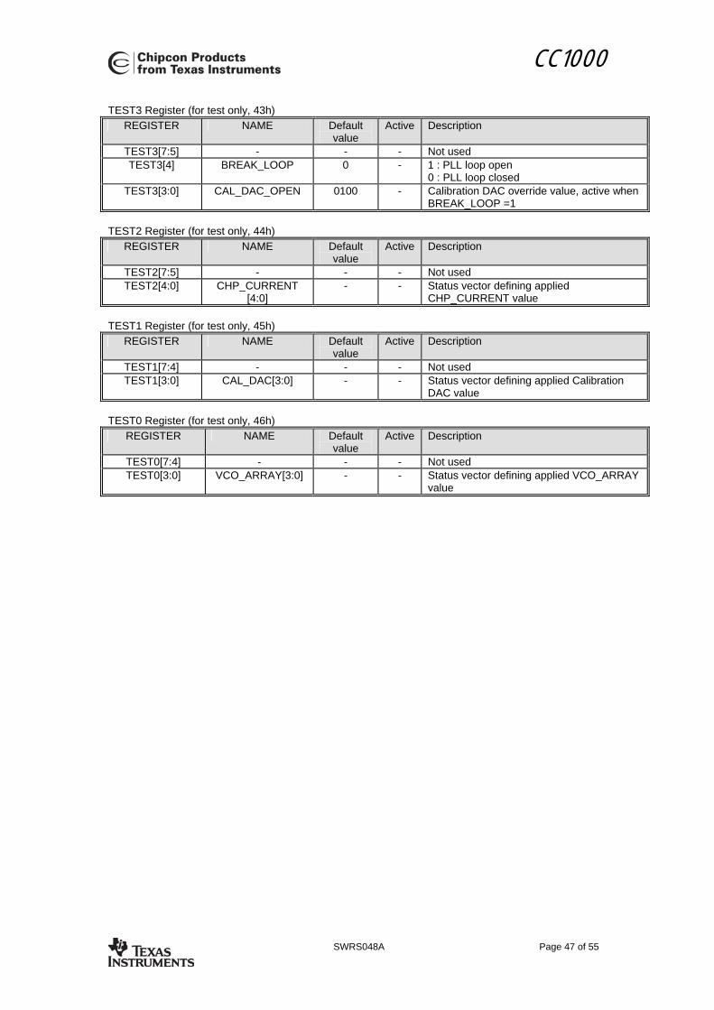
CC1000
SWRS048A Page 47 of 55
TEST3 Register (for test only, 43h) REGISTER NAME Default
value Active Description
TEST3[7:5] - - - Not used TEST3[4] BREAK_LOOP 0 - 1 : PLL loop open
0 : PLL loop closed TEST3[3:0] CAL_DAC_OPEN 0100 - Calibration DAC override value, active when
BREAK_LOOP =1 TEST2 Register (for test only, 44h)
REGISTER NAME Default value
Active Description
TEST2[7:5] - - - Not used TEST2[4:0] CHP_CURRENT
[4:0] - - Status vector defining applied
CHP_CURRENT value TEST1 Register (for test only, 45h)
REGISTER NAME Default value
Active Description
TEST1[7:4] - - - Not used TEST1[3:0] CAL_DAC[3:0] - - Status vector defining applied Calibration
DAC value TEST0 Register (for test only, 46h)
REGISTER NAME Default value
Active Description
TEST0[7:4] - - - Not used TEST0[3:0] VCO_ARRAY[3:0] - - Status vector defining applied VCO_ARRAY
value
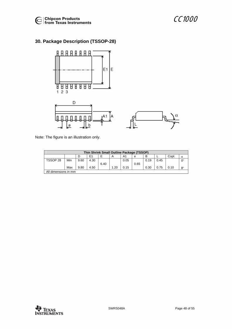
CC1000
SWRS048A Page 48 of 55
30. Package Description (TSSOP-28)
Note: The figure is an illustration only.
Thin Shrink Small Outline Package (TSSOP) D E1 E A A1 e B L Copl. α TSSOP 28 Min
Max
9.60 9.80
4.30 4.50
6.40
1.20
0.05 0.15
0.65
0.19 0.30
0.45 0.75
0.10
0° 8°
All dimensions in mm
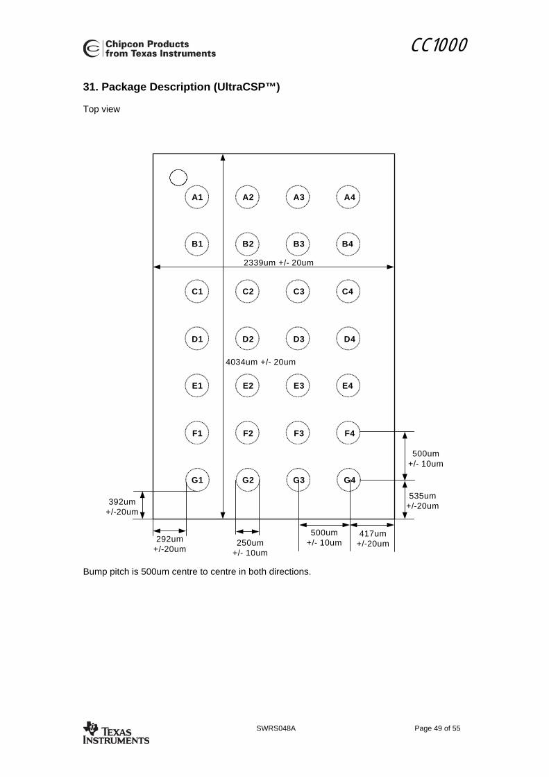
CC1000
SWRS048A Page 49 of 55
31. Package Description (UltraCSP™) Top view
250um +/- 10um
500um +/- 10um
500um +/- 10um
A1
B1
C1
D1
E1
F1
G1
A2
B2
C2
D2
E2
F2
G2
A3
B3
C3
D3
E3
F3
G3
A4
B4
C4
D4
E4
F4
G4
292um +/-20um
392um +/-20um
4034um +/- 20um
2339um +/- 20um
535um +/-20um
417um +/-20um
Bump pitch is 500um centre to centre in both directions.

CC1000
SWRS048A Page 50 of 55
Vertical cross section (UltraCSP™)
A
A
h2
h1
Die
Die
PCB mounting pads
Solder bumps (Pb free)
Before assembly on PCB:
After assembly on PCB:
Die thickness (A)
Bump height before
assembly (h1)
Bump height after assembly
(h2)
Total height before
assembly
Total height after assembly
432um 200um +/- 20um
140um +/- tbd um
632um +/- 20um
572um +/- tbd um
Table 14: Height budget
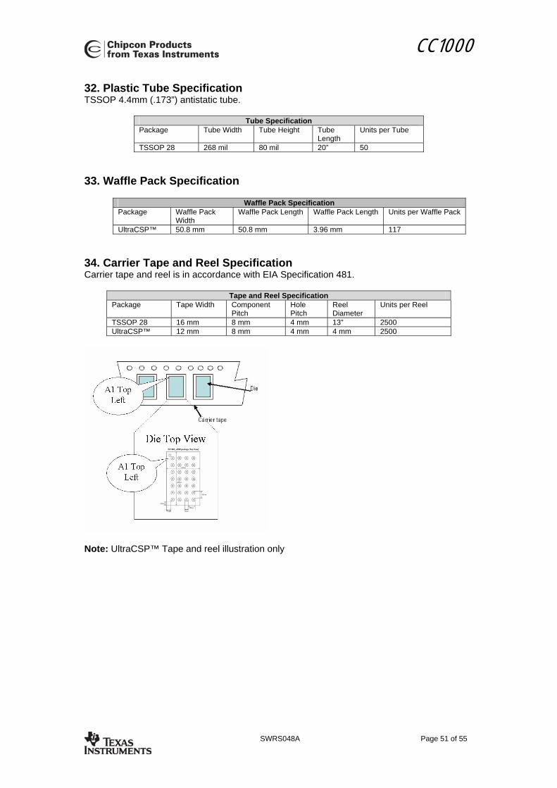
CC1000
SWRS048A Page 51 of 55
32. Plastic Tube Specification TSSOP 4.4mm (.173”) antistatic tube.
Tube Specification Package Tube Width Tube Height Tube
Length Units per Tube
TSSOP 28 268 mil 80 mil 20” 50 33. Waffle Pack Specification
Waffle Pack Specification Package Waffle Pack
Width Waffle Pack Length Waffle Pack Length Units per Waffle Pack
UltraCSP™ 50.8 mm 50.8 mm 3.96 mm 117 34. Carrier Tape and Reel Specification Carrier tape and reel is in accordance with EIA Specification 481.
Tape and Reel Specification Package Tape Width Component
Pitch Hole Pitch
Reel Diameter
Units per Reel
TSSOP 28 16 mm 8 mm 4 mm 13” 2500 UltraCSP™ 12 mm 8 mm 4 mm 4 mm 2500
Note: UltraCSP™ Tape and reel illustration only
CC1000
SWRS048A Page 52 of 55
35. Ordering Information
Chipcon Part Number*
TI Part Number Description Minimum Order Quantity (MOQ)
CC1000-RTB1 CC1000PW Single Chip RF Transceiver. CC1000, TSSOP 28 package, RoHS compliant Pb-free assembly in tubes with 50 pcs per tube.
250 (5 tubes of 50 units per tube)
CC1000-RTR1 CC1000PWR Single Chip RF Transceiver. CC1000, TSSOP 28 package, RoHS compliant Pb-free assembly, T&R with 2500 pcs per reel.
2500 (tape and reel)
CC1000-RWP2 CC1000YZ Single Chip RF Transceiver. CC1000, UltraCSP™ package, RoHS compliant Pb-free assembly with 117 pcs per waffle pack.
585 (5 waffle packs with 117 pcs per waffle pack)
CC1000-RTR2 CC1000YZR Single Chip RF Transceiver. CC1000, UltraCSP™ package, RoHS compliant Pb-free assembly, T&R with 2500 pcs per reel.
2500 (tape and reel)
CC1000DK-433 CC1000DK-433 CC1000 Development Kit, 433 MHz 1 CC1000DK-868-915 CC1000DK-868-915 CC1000 Development Kit, 868/915 MHz 1 CC1000PPK-433 CC1000PPK-433 CC1000 Plug & Play Kit, 433 MHz 1 CC1000PPK-868 CC1000PPK-868 CC1000 Plug & Play Kit, 868/915 MHz 1
* Chipcon part numbers are obsolete, but included for reference. Use the TI part numbers when ordering parts. 36. General Information 36.1 Document Revision History
Revision Date Description/Changes SWRS048A January 2007 Reflow soldering temperature according to IPC/JEDEC J-STD-020C.
Max reflow temperature for CC1000 UltraCSP™ updated to 255 °C. Added waffle pack specification. Updated ordering information with TI part numbers. Updated address information. Updated header and footer. Updated Important Notice. Removed Chipcon specific Disclaimer, Trademarks and Life Support Policy sections.
SWRS048 (2.3)
August 2005 UltraCSP™ package included Minor corrections and editorial changes
2.2 April 2004 Shaping feature removed Application circuit simplified Additional information added for the demodulator Additional information added for frequency calculation Additional information added for calibration Additional information added for crystal oscillator Preliminary version removed Narrow band information removed REFDIV different in RX and TX Minor corrections and editorial changes
36.2 Product Status Definitions
Data Sheet Identification Product Status Definition
Advance Information Planned or Under Development
This data sheet contains the design specifications for product development. Specifications may change in any manner without notice.
Preliminary Engineering Samples and First Production
This data sheet contains preliminary data, and supplementary data will be published at a later date. Chipcon reserves the right to make changes at any time without notice in order to improve design and supply the best possible product.
No Identification Noted Full Production This data sheet contains the final specifications. Chipcon reserves the right to make changes at any time without notice in order to improve design and supply the best possible product.

CC1000
SWRS048A Page 53 of 55
Data Sheet Identification Product Status Definition
Obsolete Not In Production This data sheet contains specifications on a product that has been discontinued by Chipcon. The data sheet is printed for reference information only.

CC1000
SWRS048A Page 54 of 55
37. Address Information Texas Instruments Norway AS Gaustadalléen 21 N-0349 Oslo NORWAY Tel: +47 22 95 85 44 Fax: +47 22 95 85 46 Web site: http://www.ti.com/lpw 38. TI Worldwide Technical Support Internet TI Semiconductor Product Information Center Home Page: support.ti.com TI Semiconductor KnowledgeBase Home Page: support.ti.com/sc/knowledgebase 39. Product Information Centers Americas Phone: +1(972) 644-5580 Fax: +1(972) 927-6377 Internet/Email: support.ti.com/sc/pic/americas.htm
Europe, Middle East and Africa Phone: Belgium (English) +32 (0) 27 45 54 32 Finland (English) +358 (0) 9 25173948 France +33 (0) 1 30 70 11 64 Germany +49 (0) 8161 80 33 11 Israel (English) 180 949 0107 Italy 800 79 11 37 Netherlands (English) +31 (0) 546 87 95 45 Russia +7 (0) 95 363 4824 Spain +34 902 35 40 28 Sweden (English) +46 (0) 8587 555 22 United Kingdom +44 (0) 1604 66 33 99 Fax: +49 (0) 8161 80 2045 Internet: support.ti.com/sc/pic/euro.htm
Japan Fax International +81-3-3344-5317 Domestic 0120-81-0036 Internet/Email International support.ti.com/sc/pic/japan.htm Domestic www.tij.co.jp/pic

CC1000
SWRS048A Page 55 of 55
Asia Phone International +886-2-23786800
Domestic Toll-Free Number Australia 1-800-999-084 China 800-820-8682 Hong Kong 800-96-5941 India +91-80-51381665 (Toll) Indonesia 001-803-8861-1006 Korea 080-551-2804 Malaysia 1-800-80-3973 New Zealand 0800-446-934 Philippines 1-800-765-7404 Singapore 800-886-1028 Taiwan 0800-006800 Thailand 001-800-886-0010
Fax +886-2-2378-6808 Email [email protected] or [email protected] Internet support.ti.com/sc/pic/asia.htm
Copyright © 2007, Texas Instruments Incorporated

TAPE AND REEL INFORMATION
*All dimensions are nominal
Device PackageType
PackageDrawing
Pins SPQ ReelDiameter
(mm)
ReelWidth
W1 (mm)
A0 (mm) B0 (mm) K0 (mm) P1(mm)
W(mm)
Pin1Quadrant
CC1000PWR TSSOP PW 28 2500 330.0 16.4 6.8 10.2 1.6 8.0 16.0 Q1
PACKAGE MATERIALS INFORMATION
www.ti.com 4-Feb-2009
Pack Materials-Page 1
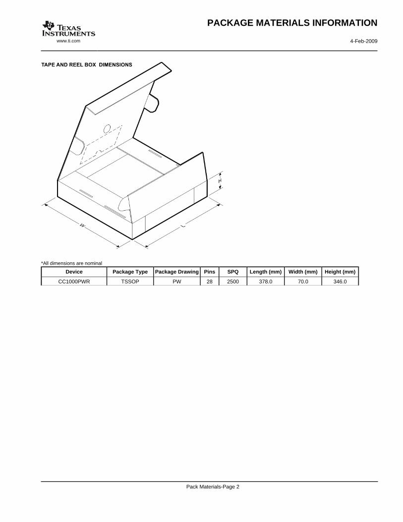
*All dimensions are nominal
Device Package Type Package Drawing Pins SPQ Length (mm) Width (mm) Height (mm)
CC1000PWR TSSOP PW 28 2500 378.0 70.0 346.0
PACKAGE MATERIALS INFORMATION
www.ti.com 4-Feb-2009
Pack Materials-Page 2
IMPORTANT NOTICETexas Instruments Incorporated and its subsidiaries (TI) reserve the right to make corrections, modifications, enhancements, improvements,and other changes to its products and services at any time and to discontinue any product or service without notice. Customers shouldobtain the latest relevant information before placing orders and should verify that such information is current and complete. All products aresold subject to TI’s terms and conditions of sale supplied at the time of order acknowledgment.TI warrants performance of its hardware products to the specifications applicable at the time of sale in accordance with TI’s standardwarranty. Testing and other quality control techniques are used to the extent TI deems necessary to support this warranty. Except wheremandated by government requirements, testing of all parameters of each product is not necessarily performed.TI assumes no liability for applications assistance or customer product design. Customers are responsible for their products andapplications using TI components. To minimize the risks associated with customer products and applications, customers should provideadequate design and operating safeguards.TI does not warrant or represent that any license, either express or implied, is granted under any TI patent right, copyright, mask work right,or other TI intellectual property right relating to any combination, machine, or process in which TI products or services are used. Informationpublished by TI regarding third-party products or services does not constitute a license from TI to use such products or services or awarranty or endorsement thereof. Use of such information may require a license from a third party under the patents or other intellectualproperty of the third party, or a license from TI under the patents or other intellectual property of TI.Reproduction of TI information in TI data books or data sheets is permissible only if reproduction is without alteration and is accompaniedby all associated warranties, conditions, limitations, and notices. Reproduction of this information with alteration is an unfair and deceptivebusiness practice. TI is not responsible or liable for such altered documentation. Information of third parties may be subject to additionalrestrictions.Resale of TI products or services with statements different from or beyond the parameters stated by TI for that product or service voids allexpress and any implied warranties for the associated TI product or service and is an unfair and deceptive business practice. TI is notresponsible or liable for any such statements.TI products are not authorized for use in safety-critical applications (such as life support) where a failure of the TI product would reasonablybe expected to cause severe personal injury or death, unless officers of the parties have executed an agreement specifically governingsuch use. Buyers represent that they have all necessary expertise in the safety and regulatory ramifications of their applications, andacknowledge and agree that they are solely responsible for all legal, regulatory and safety-related requirements concerning their productsand any use of TI products in such safety-critical applications, notwithstanding any applications-related information or support that may beprovided by TI. Further, Buyers must fully indemnify TI and its representatives against any damages arising out of the use of TI products insuch safety-critical applications.TI products are neither designed nor intended for use in military/aerospace applications or environments unless the TI products arespecifically designated by TI as military-grade or "enhanced plastic." Only products designated by TI as military-grade meet militaryspecifications. Buyers acknowledge and agree that any such use of TI products which TI has not designated as military-grade is solely atthe Buyer's risk, and that they are solely responsible for compliance with all legal and regulatory requirements in connection with such use.TI products are neither designed nor intended for use in automotive applications or environments unless the specific TI products aredesignated by TI as compliant with ISO/TS 16949 requirements. Buyers acknowledge and agree that, if they use any non-designatedproducts in automotive applications, TI will not be responsible for any failure to meet such requirements.Following are URLs where you can obtain information on other Texas Instruments products and application solutions:Products ApplicationsAmplifiers amplifier.ti.com Audio www.ti.com/audioData Converters dataconverter.ti.com Automotive www.ti.com/automotiveDLP® Products www.dlp.com Broadband www.ti.com/broadbandDSP dsp.ti.com Digital Control www.ti.com/digitalcontrolClocks and Timers www.ti.com/clocks Medical www.ti.com/medicalInterface interface.ti.com Military www.ti.com/militaryLogic logic.ti.com Optical Networking www.ti.com/opticalnetworkPower Mgmt power.ti.com Security www.ti.com/securityMicrocontrollers microcontroller.ti.com Telephony www.ti.com/telephonyRFID www.ti-rfid.com Video & Imaging www.ti.com/videoRF/IF and ZigBee® Solutions www.ti.com/lprf Wireless www.ti.com/wireless
Mailing Address: Texas Instruments, Post Office Box 655303, Dallas, Texas 75265Copyright © 2009, Texas Instruments Incorporated