Embed Size (px)
Citation preview

Si-CMOS compatible materials and devices for mid-IR microphotonics
Pao Tai Lin,1,* Vivek Singh,1 Jianfei Wang,1 Hongtao Lin,2 Juejun Hu,2 Kathleen Richardson,3 J. David Musgraves,4 Igor Luzinov,4 Joel Hensley,5 Lionel C. Kimerling,1
and Anu Agarwal1 1Materials Processing Center, Massachusetts Institute of Technology, Cambridge, MA, 02139 USA
2Department of Materials Science and Engineering, University of Delaware, DE, 19716 USA 3The College of Optics & Photonics (CREOL), University of Central Florida. Orlando, Florida, 32816 USA
4Department of Materials Science and Engineering, Clemson University, Clemson, South Carolina 29634 USA 5Physical Sciences Inc., 20 New England Business Center, Andover, MA 01810 USA
Abstract: CMOS compatible mid-Infrared (mid-IR) microphotonics including (1) broadband SOUP (Silicon on Oxide Undercladding Pedestal) waveguides; and (2) mid-IR transparent chalcogenide glass (ChGs) waveguides monolithically integrated with a PbTe thin film photodetector; are demonstrated. Using a pedestal undercladding geometry we obtain an optical loss for our Si waveguide which is 10 dB/cm lower compared to other waveguides using planar SiO2 cladding at λ = 5 µm, and a fundamental mode is seen over a broad mid-IR spectral range. To realize a fully integrated mid-IR on-chip system, in parallel, we develop PbTe thin film detectors that can be deposited on various mid-IR platforms through a thermal evaporation technique, offering high photoresponsivity of 25 V/W from λ = 1 µm to 4 µm. The detector can be efficiently integrated, using a suitable spacer, to an underlying Chalcogenide glass (ChGs) waveguide. Our results of low loss waveguides and integrated thin film detectors enable Si-CMOS microphotonics for mid-IR applications.
©2013 Optical Society of America
OCIS codes: (130.3120) Integrated optics devices; (130.3130) Integrated optics materials; (130.3060) Infrared.
References and links
1. D. Psaltis, S. R. Quake, and C. Yang, “Developing optofluidic technology through the fusion of microfluidics and optics,” Nature 442(7101), 381–386 (2006).
2. X. Fan and I. M. White, “Optofluidic microsystems for chemical and biological analysis,” Nat. Photonics 5(10), 591–597 (2011).
3. J. Ozhikandathil and M. Packirisamy, “Silica-on-silicon waveguide integrated polydimethylsiloxane lab-on-a-chip for quantum dot fluorescence bio-detection,” J. Biomed. Opt. 17(1), 017006 (2012).
4. A. Chandrasekaran and M. Packirisamy, “Integrated microfluidic biophotonic chip for laser induced fluorescence detection,” Biomed. Microdevices 12(5), 923–933 (2010).
5. K. Reddy, Y. Guo, J. Liu, W. Lee, M. K. Oo, and X. Fan, “Rapid, sensitive, and multiplexed on-chip optical sensors for micro-gas chromatography,” Lab Chip 12(5), 901–905 (2012).
6. M. M. Milošević, M. Nedeljkovic, T. M. Ben Masaud, E. Jaberansary, H. M. H. Chong, N. G. Emerson, G. T. Reed, and G. Z. Mashanovich, “Silicon waveguides and devices for the mid-infrared,” Appl. Phys. Lett. 101(12), 121105 (2012).
7. R. K. W. Lau, M. Ménard, Y. Okawachi, M. A. Foster, A. C. Turner-Foster, R. Salem, M. Lipson, and A. L. Gaeta, “Continuous-wave mid-infrared frequency conversion in silicon nanowaveguides,” Opt. Lett. 36(7), 1263–1265 (2011).
8. P. T. Lin, V. Singh, H.-Y. G. Lin, T. Tiwald, L. C. Kimerling, and A. M. Agarwal, “Low-stress silicon nitride platform for mid-infrared broadband and monolithically integrated microphotonics,” Adv. Opt. Mater. doi: 10.1002/adom.201300205 (2013).
9. X. Liu, R. M. Osgood, Jr., Y. A. Vlasov, and W. M. J. Green, “Mid-infrared optical parametric amplifier using silicon nanophotonic waveguides,” Nat. Photonics 4(8), 557–560 (2010).
10. P. Y. Yang, S. Stankovic, J. Crnjanski, E. J. Teo, D. Thomson, A. A. Bettiol, M. B. H. Breese, W. Headley, C. Giusca, G. T. Reed, and G. Z. Mashanovich, “Silicon photonic waveguides for mid- and long-wave infrared region,” J. Mater. Sci. Mater. Electron. 20(S1), 159–163 (2009).
#193108 - $15.00 USD Received 1 Jul 2013; revised 14 Aug 2013; accepted 14 Aug 2013; published 26 Aug 2013(C) 2013 OSA 1 September 2013 | Vol. 3, No. 9 | DOI:10.1364/OME.3.001474 | OPTICAL MATERIALS EXPRESS 1474

11. G. Z. Mashanovich, M. M. Milošević, M. Nedeljkovic, N. Owens, B. Xiong, E. J. Teo, and Y. Hu, “Low loss silicon waveguides for the mid-infrared,” Opt. Express 19(8), 7112–7119 (2011).
12. R. Soref, “Mid-infrared photonics in silicon and germanium,” Nat. Photonics 4(8), 495–497 (2010). 13. H. Gunzler and H. U. Gremlich, IR Spectroscopy: An Introduction (Wiley-VCH, 2002). 14. R. M. Silverstein, F. X. Webster, and D. Kiemle, Spectrometric Identification of Organic Compounds (Wiley,
2005). 15. R. A. Soref, S. J. Emelett, and W. R. Buchwald, “Silicon waveguided components for the long-wave infrared
region,” J. Opt. A, Pure Appl. Opt. 8(10), 840–848 (2006). 16. Y. Wei, G. Li, Y. Hao, Y. Li, J. Yang, M. Wang, and X. Jiang, “Long-wave infrared 1 × 2 MMI based on air-gap
beneath silicon rib waveguides,” Opt. Express 19(17), 15803–15809 (2011). 17. P. T. Lin, V. Singh, L. Kimerling, and A. M. Agarwal, “Planar silicon nitride mid-infrared devices,” Appl. Phys.
Lett. 102(25), 251121 (2013). 18. G. Z. Mashanovich, M. M. Milošević, M. Nedeljkovic, N. Owens, B. Xiong, E. J. Teo, and Y. Hu, “Low loss
silicon waveguides for the mid-infrared,” Opt. Express 19(8), 7112–7119 (2011). 19. P. Y. Yang, G. Z. Mashanovich, I. Gomez-Morilla, W. R. Headley, G. T. Reed, E. J. Teo, D. J. Blackwood, M.
B. H. Breese, and A. A. Bettiol, “Freestanding waveguides in silicon,” Appl. Phys. Lett. 90(24), 241109 (2007). 20. T. Baehr-Jones, A. Spott, R. Ilic, A. Spott, B. Penkov, W. Asher, and M. Hochberg, “Silicon-on-sapphire
integrated waveguides for the mid-infrared,” Opt. Express 18(12), 12127–12135 (2010). 21. F. Li, S. D. Jackson, C. Grillet, E. Magi, D. Hudson, S. J. Madden, Y. Moghe, C. O’Brien, A. Read, S. G.
Duvall, P. Atanackovic, B. J. Eggleton, and D. J. Moss, “Low propagation loss silicon-on-sapphire waveguides for the mid-infrared,” Opt. Express 19(16), 15212–15220 (2011).
22. P. T. Lin, V. Singh, J. Hu, K. Richardson, J. D. Musgraves, I. Luzinov, J. Hensley, L. C. Kimerling, and A. Agarwal, “Chip-scale Mid-Infrared chemical sensors using air-clad pedestal silicon waveguides,” Lab Chip 13(11), 2161–2166 (2013).
23. P. T. Lin, V. Singh, Y. Cai, L. C. Kimerling, and A. Agarwal, “Air-clad silicon pedestal structures for broadband mid-infrared microphotonics,” Opt. Lett. 38(7), 1031–1033 (2013).
24. A. Rogalski, “Infrared detectors: status and trends,” Prog. Quantum Electron. 27(2-3), 59–210 (2003). 25. Lead Selenide Detectors, Available: http://www.judsontechnologies.com/lead_sel.html 26. D. E. Bode, Lead Salt Detectors vol. 3 (Academic Press, 1966). 27. J. Wang, J. Hu, X. Sun, A. Agarwal, D. Lim, R. Synowicki, and L. Kimerling, “Structural, electrical and optical
properties of thermally evaporated nanocrystalline PbTe films,” J. Appl. Phys. 104(5), 053707 (2008). 28. J. Wang, T. Zens, J. Hu, P. Becla, L. C. Kimerling, and A. M. Agarwal, “Monolithically integrated, resonant-
cavity-enhanced dual-band mid-infrared photodetector on silicon,” Appl. Phys. Lett. 100(21), 211106 (2012). 29. M. Böberl, T. Fromherz, J. Roither, G. Pillwein, G. Springholz, and W. Heiss, “Room temperature operation of
epitaxial lead-telluride detectors monolithically integrated on midinfrared filters,” Appl. Phys. Lett. 88(4), 041105 (2006).
30. J. Wang, J. Hu, P. Becla, A. M. Agarwal, and L. Kimerling, “Room-temperature oxygen sensitization in highly textured, nanocrystalline PbTe films: A mechanistic study,” J. Appl. Phys. 110(8), 083719 (2011).
31. J. Wang thesis, “Resonant-cavity-enhanced Multispectral Infrared Photodetectors for Monolithic Integration on Silicon,” Ph.D., Materials Science and Engineering, Massachusetts Institute of Technology, Cambridge, MA (2010).
32. R. L. Petritz, “Theory of Photoconductivity in Semiconductor Films,” Phys. Rev. 104(6), 1508–1516 (1956). 33. J. C. Slater, “Barrier Theory of the Photoconductivity of Lead Sulfide,” Phys. Rev. 103(6), 1631–1644 (1956). 34. A. Gassenq, N. Hattasan, L. Cerutti, J. B. Rodriguez, E. Tournié, and G. Roelkens, “Study of evanescently-
coupled and grating-assisted GaInAsSb photodiodes integrated on a silicon photonic chip,” Opt. Express 20(11), 11665–11672 (2012).
35. D. Ahn, C. Y. Hong, J. Liu, W. Giziewicz, M. Beals, L. C. Kimerling, J. Michel, J. Chen, and F. X. Kärtner, “High performance, waveguide integrated Ge photodetectors,” Opt. Express 15(7), 3916–3921 (2007).
36. NIST Chemistry WebBook, http://webbook.nist.gov/chemistry 37. C. Y. Liang and S. Krimm, “Infrared Spectra of High Polymers–Part IX: Polyethylene Terephthalate,” J. Mol.
Spectrosc. 3(1-6), 554–574 (1959). 38. H. Lin, L. Li, Y. Zou, S. Danto, J. D. Musgraves, K. Richardson, S. Kozacik, M. Murakowski, D. Prather, P. T.
Lin, V. Singh, A. Agarwal, L. C. Kimerling, and J. Hu, “Demonstration of high-Q mid-infrared chalcogenide glass-on-silicon resonators,” Opt. Lett. 38(9), 1470–1472 (2013).
1. Introduction
Mid-IR microphotonics has attracted significant attention because of its application in biochemical detection and toxic gas/liquid monitoring [1–5]. Among the variety of available mid-IR materials, the silicon platform is considered favorably because of its CMOS compatibility, robust mechanical/chemical properties and broad mid-IR transparency up to λ = 8 µm [6–9]. Current silicon microphotonic devices are developed on a silicon-on-insulator (SOI) platform that has crystalline silicon waveguides with a silicon dioxide under-cladding. Although SOI technology has been instrumental in advancing near infrared (NIR) integrated photonics, adopting the same platform for planar mid-IR devices remains a challenge because the optical loss of silicon dioxide sharply increases beyond λ of 3.6 µm [10–12]. Thus, it
#193108 - $15.00 USD Received 1 Jul 2013; revised 14 Aug 2013; accepted 14 Aug 2013; published 26 Aug 2013(C) 2013 OSA 1 September 2013 | Vol. 3, No. 9 | DOI:10.1364/OME.3.001474 | OPTICAL MATERIALS EXPRESS 1475

becomes impractical to utilize NIR SOI microphotonics for on-chip chemical sensing (finger-printing spectrometry) of some double-bond functional groups such as C = O, C = N and C = C, that have vibrational absorption between λ = 5 µm and λ = 8 µm [13,14]. To extend the feasibility of silicon based planar devices beyond λ = 3.6 µm several approaches have been investigated [15–17]. For instance, a platform using crystalline silicon on porous silicon (SiPSi) was proposed for mid-IR devices, where the waveguide cladding is a porous silicon layer created by high-energy proton beam irradiation followed by electrochemical etching [18, 19]. Even though the porous under-cladding has a lower refractive index, scattering loss and material damage from high energy irradiation has not been adequately investigated. Another option is a silicon-on-sapphire (SOS) platform where the mid-IR opaque silicon dioxide in SOI devices is replaced by sapphire which has a broader transmission up to 4.5 µm [20, 21]. Nevertheless, to utilize the full transparency window of crystalline Si (up to λ = 8 µm) a new device design is required [22, 23].
To solve the problem of optical loss caused by the oxide cladding, we illustrate a novel structure: that of a mid-IR silicon waveguide supported by a carefully engineered oxide pedestal as the under-cladding. We will refer to it as our SOUP (Silicon on Oxide Undercladding Pedestal) waveguide. The performance of the proposed SOUP waveguide is designed and optimized using Finite Difference Method (FDM). The mid-IR response, including optical loss and effective refractive indices, are investigated as wavelength is scanned from λ = 2 µm to λ = 8 µm. From the simulation, we demonstrate that optical loss can be decreased considerably when the under-cladding is modified into a pedestal. In addition, the desired structure can be generated through an isotropic undercut process so the entire fabrication is CMOS-compatible and amenable to large-scale manufacturing. Our scanning electron microscope (SEM) image confirms that the structure of the silicon waveguide and underlying oxide pedestal were well maintained throughout the processing sequence. Clearly resolved waveguide modes indicate that these SOUP structures are promising waveguiding components for integrated mid-IR microphotonics.
In addition to these low-loss mid-IR SOUP waveguides, we need on-chip detection of transmitted mid-IR light. Typically, HgCdTe and III-V compounds such as InAs and InSb are used for mid-IR detection and spectroscopy applications. However, these are obtained by growth techniques such as metal organic chemical vapor deposition (MOCVD) or Molecular Beam Epitaxy (MBE) which are not only high in cost, but are incompatible with silicon monolithic integration [24]. Lead salts or lead chalcogenides such as PbTe, PbSe, and PbS form another set of materials suitable for this wavelength range, and mid-IR detectors based on crystalline PbSe and PbS are already commercially available [25]. Additionally, PbTe is a promising candidate for integrated low cost and robust IR detection technology due to its superior chemical stability and the ease of deposition [26, 27]. Single crystal PbTe has been studied for the fabrication of on-chip IR photodetectors and long wavelength laser devices [28]. Epitaxial PbTe detectors integrated with mid-IR filters have demonstrated enhanced photoresponsivity at room temperature while high detectivity has also been obtained with polycrystalline PbTe films [29, 30]. Polycrystalline PbTe is relatively easy to deposit on many kinds of substrates using low-cost thermal evaporation techniques at room temperature. We demonstrate on-chip patterning of thin film polycrystalline PbTe photoconductors by using a negative resist lift-off photolithography process. Finally, we show that alloying PbTe with tin telluride (SnTe) to form PbxSn1-xTe offers the ability to tune the optical band gap of the material and extend detection capabilities to the 6-12 µm regime.
2. Mid-IR crystalline Si waveguide with silicon dioxide pedestal undercladding
2.1 Device design and simulation results of pedestal oxide waveguide
Figure 1(a) illustrates the structure of the proposed SOUP waveguide for mid-IR applications: a device consisting of a single crystalline Si core with an oxide pedestal as an undercladding. Crystalline Si is chosen as the light guiding material because of its broad mid-IR transmittance as well as its high refractive index in order to achieve substantial wave
#193108 - $15.00 USD Received 1 Jul 2013; revised 14 Aug 2013; accepted 14 Aug 2013; published 26 Aug 2013(C) 2013 OSA 1 September 2013 | Vol. 3, No. 9 | DOI:10.1364/OME.3.001474 | OPTICAL MATERIALS EXPRESS 1476

confinement. On the other hand, the undercladding is mostly an air gap with an oxide pedestal where both oxide and air have much lower refractive index compared to the Si waveguide core. Thus, a large refractive index contrast is obtained between the waveguide core and cladding and as a result the SOUP waveguide can efficiently prevent leakage of the guided mid-IR light into the high index Si substrate wafer. Furthermore, by replacing the mid-IR opaque oxide by air can significantly reduce the optical loss seen in SOI devices. The main structure parameters which determine the device performance include waveguide width w, waveguide height h, pedestal height s, notch width d and undercut radius r. For instance, the mode profiles and effective refractive indices depend on w and h. Likewise the propagation loss is mainly associated with s, d and r. To better visualize the refractive index profile of the proposed SOUP waveguide, the index map is drawn in Fig. 1(b). The Si waveguide with index of 3.4 is defined from −1 µm to 1 µm along the y axis and from 0 µm to 2 µm along the z axis, which gives w = 2 µm and h = 2 µm, respectively. Two air hemispheres that serve as the etched areas of the oxide undercladding are centered at x = −1 and x = 1 with a radius r of 0.8 µm. Thus, the contact length between oxide pedestal and silicon waveguide, which we define as the notch width d, is 0.4 µm. Based on the designed structure shown in Fig. 1(b), we use FEM method to calculate the corresponding mode profile and the result is shown in Fig. 1(c). A clear fundamental mode is obtained within the upper Si waveguide core at a wavelength λ of 5 µm. Furthermore, there is only negligible mid-IR light observed in the surrounding air cladding or oxide pedestal because the refractive index contrast between Si and air/oxide is large. Thus, we show that our design of the mid-IR SOUP waveguide can efficiently guide long wavelength light in the Si core as well as minimize optical loss caused by the undercladding.
Fig. 1. (a) The structure of the proposed SOUP (Silicon on Oxide Undercladding Pedestal) mid-IR waveguide device consists of a crystalline Si core and a pedestal oxide undercladding. The structure parameters include waveguide width w, waveguide height h, pedestal height s, notch width d and undercut radius r. (b) The refractive index profile of the proposed waveguide. (c) The calculated mode profile shows a clear fundamental mode within the upper Si waveguide core at wavelength λ of 5 µm.
To investigate the performance of the SOUP mid-IR waveguide, optical losses and effective refractive indices are calculated for different device geometries at λ = 5 µm. The waveguide structure is as shown in Fig. 1(b) with w = 2 µm and h = 2 µm, except the undercut radius r is gradually increased from 0 µm to 1.2 µm. The results of our simulations are shown in Fig. 2(a), from which we see that the optical loss decreases notably from 9.5 dB/cm (at r = 0 µm) to 0.2 dB/cm (at r = 1 µm). We note that r = 0 µm indicates all oxide cladding remains and the Si waveguide is in full contact with the underlying oxide layer. On the other hand, at r = 1 µm the entire oxide undercladding is removed and there is no contact between the Si core and the oxide layer. Thus, the significant drop in optical loss as r increases is clearly attributed to the implementation of a pedestal structure where the undercladding mid-IR opaque oxide is replaced by air that has no mid-IR loss. Additionally, the effective refractive index of a waveguide with different undercut radius r is shown in Fig. 2(b). Only a trivial variation of effective indices is seen with a change in r, leading to the
#193108 - $15.00 USD Received 1 Jul 2013; revised 14 Aug 2013; accepted 14 Aug 2013; published 26 Aug 2013(C) 2013 OSA 1 September 2013 | Vol. 3, No. 9 | DOI:10.1364/OME.3.001474 | OPTICAL MATERIALS EXPRESS 1477

conclusion that mid-IR light is well guided by the Si core after most of oxide cladding is replaced by air. Thus, we confirm that the SOUP waveguide is suitable for mid-IR operation and it overcomes the “lossy oxide” challenge of the SOI platform.
Fig. 2. (a) the optical loss shows a significant drop as r increases and can be attributed to the implementation of a pedestal structure where the undercladding mid-IR opaque oxide is replaced by air that has no mid-IR loss. and (b) the effective refractive index shows almost no change as a function of undercut radius r at λ = 5 µm. The waveguide structure has w = 2 µm and h = 2 µm. Mid-IR light is well guided by the Si core after most of the oxide cladding is replaced by air.
The performance of the SOUP waveguide is evaluated at different mid-IR wavelengths. Figure 3(a) shows the mode profiles calculated at λ = 2 µm, λ = 4 µm and λ = 6 µm, where the structure used in the FEM simulation has parameters of w = 2 µm, h = 2 µm, r = 0.8 µm and d = 0.4 µm. At λ = 2 µm the intensity peak of the fundamental mode is aligned with the center of the Si core, and the evanescent waves are barely observed outside the waveguide edges. As the wavelength tunes to λ = 4 µm the mode expands because the wavelength increases and a dim evanescent wave starts to appear in the undercladding. Once the wavelength shifts to λ = 6 µm, the mode size grows and extends beyond the boundary between the waveguide and the undercladding. An evanescent wave is seen to extend beneath the waveguide into the undercladding as wavelength increases, and belies the importance of choice of undercladding material for low-loss performance. To better appreciate the advantages of our SOUP waveguide, Fig. 3(b) shows the optical loss improvement as a function of transmitted wavelength, where the improvement is defined as the decrease in waveguide loss before and after oxide pedestal formation. The loss improvement sharply increases from 0.1 dB/cm to 10 dB/cm as wavelength shifts from λ = 4 µm to λ = 5 µm because the absorption in silicon dioxide rises strongly after λ = 3.5 µm and the effect of oxide removal becomes critical for obtaining low loss mid-IR waveguides. The increasing trend of “optical loss improvement” continues even after λ = 5 µm. In addition, Si has negligible two photon absorption at longer wavelengths (λ > 2.2 µm). On the other hand, at a short wavelength of λ < 3.5 µm, the loss improvement is minor because silicon dioxide has a high transparency within this spectral region and so there is no significant advantage to etching the oxide undercladding to form a pedestal. The effective refractive index, neff, of the mid-IR pedestal waveguide is calculated for the mid-IR spectral range and the result is shown in Fig. 3(c). We see a drop in neff from 3.4 to 2.6 as the wavelength shifts from λ = 2.5 µm to λ = 7.5 µm. This decrease is attributed to the expansion of the evanescent wave into the air cladding as the wavelength increases, thereby underscoring the importance of etching out the mid-IR opaque oxide for long wavelength operation.
#193108 - $15.00 USD Received 1 Jul 2013; revised 14 Aug 2013; accepted 14 Aug 2013; published 26 Aug 2013(C) 2013 OSA 1 September 2013 | Vol. 3, No. 9 | DOI:10.1364/OME.3.001474 | OPTICAL MATERIALS EXPRESS 1478

Fig. 3. (a) The calculated mode profiles at λ = 2 µm, 4 µm and λ = 6 µm where the structure parameters are w = 2 µm, h = 2 µm, r = 0.8 µm and d = 0.4 µm. As wavelength increases, the evanescent wave extends beneath the waveguide into the undercladding, and belies the importance of choice of undercladding material for low-loss performance. (b) The optical loss improvement increases with increasing wavelength. Here the improvement is defined by the decrease of waveguide loss before and after oxide undercut and (c) The effective refractive index neff decreases as a function of wavelength, because the evanescent mode expands to the undercladding.
2.2 Fabrication and characterization of the SOUP waveguide
To fabricate the SOUP structure a multistep process consisting of dry/wet etching is used. The detailed fabrication scheme is shown in Fig. 4(a). At Step (i) waveguide patterns are generated on an SOI wafer via conventional photolithography. At Step (ii) the patterns are transferred into the top Si layer with an inductively coupled plasma reactive ion etching (ICP-RIE) process. At Step (iii) the photoresist used for pattern generation is removed by acetone and plasma cleaning. At Step (iv) undercut of oxide cladding is performed by isotropic buffered oxide etch (BOE). The fabricated mid-IR waveguides were inspected by SEM and an image is shown in Fig. 4(b). The sample is tilted at 54° during microscopy to improve the cross sectional image. From Fig. 4(b), the waveguide surface, edge and facet is seen to be smooth and crack-free. In addition, the undercut oxide successfully supports the upper Si core and the structure parameters are obtained as w = 3 µm, h = 2 µm, r = 1.8 µm and d = 0.5 µm. The chosen of 3 µm wide Si waveguide is to prevent over etching of undercut oxide.
#193108 - $15.00 USD Received 1 Jul 2013; revised 14 Aug 2013; accepted 14 Aug 2013; published 26 Aug 2013(C) 2013 OSA 1 September 2013 | Vol. 3, No. 9 | DOI:10.1364/OME.3.001474 | OPTICAL MATERIALS EXPRESS 1479

Fig. 4. (a) Fabrication process of the SOUP waveguide. At Step (i) patterns of waveguide are generated on a SOI wafer via conventional photolithography. At Step (ii) the patterns are transferred into top Si layer with ICP-RIE. At Step (iii) the photoresist used for pattern generation is removed by acetone and plasma cleaning. At Step (iv) under-cut of oxide cladding is performed by BOE. (b) SEM image of fabricated SOUP waveguide showing measured structure parameters as w = 3 µm, h = 2 µm r = 1.8 µm and d = 0.5 µm. The waveguide integrity is maintained and its surface, edge and facet is seen to be smooth and crack-free.
To experimentally evaluate the performance of the SOUP waveguides we set up a mid-IR test platform as illustrated in Fig. 5(a). The light source used is a pulsed laser with 150 mW average power and a pulse repetition rate of 150 kHz. The laser wavelength is tunable from λ = 2.4 μm to λ = 3.7 μm with a line width of 3 cm−1. Using a reflective lens the probe light is first collimated into a 9 µm core and 125 μm cladding fluoride fiber. Alignment between the optical fiber and the waveguide is achieved using high precision positioning stages with 0.02 μm sensitivity. This fine adjustment is monitored by an upper microscope equipped with a long working-distance objective. The mid-IR signals from the waveguides are focused by a calcium fluoride bi-convex lens with 25 mm focal length and then imaged by liquid nitrogen cooled 320 x 256 pixel InSb camera. The mode of the SOUP waveguide is captured by the mid-IR camera at λ = 3.7 µm and depicted in Fig. 5(b). The intensity profile across the x axis is shown in Fig. 5(c). A sharp fundamental mode is clearly resolved and no scattering or distortion is seen which indicates that the mid-IR light is well confined inside the SOUP waveguide as predicted by the FEM simulation. In addition, the fundamental mode remains the dominant mode within the wide spectral range and the low optical loss of crystalline Si is confirmed by Fourier transform infrared spectroscopy (FTIR) measurements indicating that the undercut SOUP waveguides are suitable for broadband mid-IR planar devices.
Fig. 5. (a) The experimental setup for mid-IR waveguide characterization. The light source from a tunable laser (λ = 2.4 μm to λ = 3.7 μm) is butt-coupled into the SOUP waveguide through a fluoride fiber. (b) The waveguide fundamental mode is captured by the mid-IR camera at λ = 3.7 µm. (c) The mode intensity profile along the x axis.
#193108 - $15.00 USD Received 1 Jul 2013; revised 14 Aug 2013; accepted 14 Aug 2013; published 26 Aug 2013(C) 2013 OSA 1 September 2013 | Vol. 3, No. 9 | DOI:10.1364/OME.3.001474 | OPTICAL MATERIALS EXPRESS 1480

3. CMOS compatible mid-IR chalcogenide glass waveguides with integrated PbTe detectors
3.1 Performance of PbTe thin film photoconductors
A systematic investigation of the structural, electrical, and optical properties of polycrystalline PbTe films, essential for device design and performance, has been conducted previously [31]. Thin films evaporated on different substrates were demonstrated to be stoichiometric, single fcc phase (rock salt structure), polycrystalline with (200) texture, with RMS surface roughness of 14–16 nm and grain sizes on the order of 50–100 nm. Electrical characterization of evaporated films shows thermally activated p-type conduction with a mobility of 53 cm2/V.s and a room temperature carrier concentration of 2.1 × 1017 cm−3. The direct optical band gap of 0.386 eV is higher than the bulk value of 0.31 eV, likely due to quantum confinement effects. Sub-band gap absorption was observed between 0.2 and 0.4 eV, attributed to defect states due to the polycrystalline nature of the PbTe films.
Figure 6 shows the photoresponsivity of polycrystalline PbTe films of different thicknesses at room temperature and at thermoelectrically-cooled temperatures (−60°C or 213 K). We have found that a 100 nm thick PbTe detector layer exhibits high photoresponsivity (25 V/W) in the 3-4 µm wavelength range of interest under a bias current of 0.1 mA at −60°C; the responsivity is between 1.2 to 3.5 times larger than a 200 nm film, pointing to a dependence of responsivity on film thickness. This thickness dependence of responsivity can be explained by the number modulation theory [32, 33] which attributes the source of photoconductivity in lead chalcogenide materials to a change in the carrier concentration rather than a change in carrier mobility.
Fig. 6. Responsivity of polycrystalline PbTe films of different thicknesses under a bias current of 0.1 mA and cooled to −60°C (by a TEC). The 100 nm film exhibits the highest responsivity in the 3-4 µm wavelength range [31].
3.2 Enhancing quantum efficiency and enabling multi-spectral detection via resonant cavity structures
Since PbTe is a direct bandgap material, we can define the quantum efficiency (QE) as the fraction of incident radiation absorbed assuming all incident photons generate electron-hole pairs. Although we find that the responsivity of our PbTe thin film increases with decreasing thickness, the QE actually decreases with decreasing film thickness. The disparity in QE is low at shorter wavelengths due to the higher absorption coefficient of PbTe at these wavelengths but it is much larger in the 3-4 µm wavelength range where thicker films allow more of the light to be absorbed.
As the responsivity is directly proportional to the QE and inversely proportional to the square of the thickness, attempting to increase the quantum efficiency while simultaneously
#193108 - $15.00 USD Received 1 Jul 2013; revised 14 Aug 2013; accepted 14 Aug 2013; published 26 Aug 2013(C) 2013 OSA 1 September 2013 | Vol. 3, No. 9 | DOI:10.1364/OME.3.001474 | OPTICAL MATERIALS EXPRESS 1481

decreasing film thickness can yield significant increases in responsivity. Further, since the detector noise scales with the square root of the active material volume, thinner films will lead to a higher signal-to-noise (SNR) ratio. Thus, to enhance the QE of our PbTe thin films, we have developed resonant cavity structures that enable higher absorption even as film thickness is decreased. As shown in Fig. 7, the resonant cavity enhanced (RCE) design consists of a thin layer of PbTe sandwiched between Distributed Bragg Reflector (DBR) stacks made up of alternating layers of arsenic sulfide (As2S3) and germanium (Ge) that are both transparent in the mid-IR [28, 31]. Thermally evaporated As2S3 serves as the low index material while sputtered germanium is the high index material, yielding a high refractive index contrast stack. Both materials can be deposited layer by layer within a single vacuum deposition chamber without breaking vacuum. By designing the DBR stacks to achieve critical coupling at the resonant wavelength, we can obtain near unity QE. Our experimental results show that a peak responsivity as high as 800 V/W can be obtained at −55°C under a bias current of 0.06 mA at a wavelength of about 3.4 µm for a 400 µm x 400 µm RCE photodetector with a 100 nm thick PbTe absorbing layer. Smaller detector widths should lead to further improvements as the responsivity scales inversely with the square of the width.
Fig. 7. Schematic cross-sectional image of the designed resonant cavity structure. The cavity region consists of a thin, absorbing PbTe layer sandwiched between two As2S3 layers [28, 31].
Multispectral IR detection is an important feature necessary in several applications such as hyperspectral imaging, spectroscopy, and target identification. We can design an RCE structure involving a multilayer cascaded cavity where each wavelength to be detected leads to a unique resonant cavity mode and has a dedicated, spectrally selective absorbing active layer. By using multiple cavities, spectral cross-talk can be reduced and the electrical signal can be read separately for each absorbing layer. We have designed and fabricated a two-color multispectral detector on a silicon substrate operating at 1.61 µm and 3.7 µm with peak quantum efficiencies as high as 0.92 and 0.68 respectively.
3.3 Integrating PbTe detectors with chalcogenide glass waveguides for lab-on-a-chip sensing applications
Figure 8 shows a schematic illustration of a lab-on-a-chip sensor system that combines a light source, sensing elements, a detector, and read-out circuitry on a monolithic silicon platform. We use Chalcogenide glasses (ChGs) as waveguides for this system. ChGs are inorganic, amorphous compounds of chalcogen elements (sulfur, selenium, and/or tellurium) with other metal or non-metal elements, and have been recognized as a material of choice for infrared (IR) applications such as chemical and biological sensing due to their wide optical transparency in the mid- and far-infrared wavelength regions. ChGs exhibit tunable optical properties through doping and/or compositional tailoring and a Si-CMOS-backend-compatible process can be used to fabricate planar devices. Monolithic integration of elements such as a light source, sensor element, detector, and read-out circuitry on to a silicon platform enables low cost, high sensitivity detection in a small footprint. Further, the reduction of device footprints can lead to their use in remotely deployable arrays of integrated mid-IR sensor devices.
#193108 - $15.00 USD Received 1 Jul 2013; revised 14 Aug 2013; accepted 14 Aug 2013; published 26 Aug 2013(C) 2013 OSA 1 September 2013 | Vol. 3, No. 9 | DOI:10.1364/OME.3.001474 | OPTICAL MATERIALS EXPRESS 1482

Fig. 8. Schematic of a mid-IR lab-on-a-chip sensor system that combines a light source, sensing elements, a detector, and read-out circuitry on a monolithic silicon platform. The functionalization layer adds specificity to the sensor response for greater accuracy in analyte recognition.
3.3.1 Design of ChG waveguides (As2Se3) integrated with mid-IR PbTe detectors
Our approach to an integrated sensor design uses vertical evanescent coupling from ChG waveguides (As2Se3) into mid-IR PbTe detectors. An inherent challenge is the large index difference between As2Se3 (n = 2.75) and PbTe (n = 5.2) which is addressed by the introduction of a low index spacer layer between the waveguide and detector to minimize modal mismatch and Fresnel reflection. This significantly increases the absorption length in the detector compared to a similar structure without a spacer. Evanescently-coupled detectors using hybrid integration of III-V detectors for 2.2–2.3 μm detection and monolithically integrated Ge detectors for telecom wavelengths have been demonstrated [34, 35].We propose a ChG waveguide monolithically integrated with an MWIR PbTe detector. Figure 9 (a) shows the layout of the evanescently coupled detector and Fig. 9 (b) shows a cross section of the detector waveguide system. The As2Se3 waveguide is designed for single mode operation at 3.2 μm and the GeSbS glass (n = 2.1) undercladding prevents leakage into the silicon substrate. The spacer (nominally n = 1.5) in Fig. 4 covers the entire sample, with the PbTe extending laterally beyond the waveguide.
Fig. 9. (a) Integrated detector structure with a single mode (λ = 3.2 µm) As2Se3 waveguide, GeSbS glass undercladding to prevent leakage of mode into Si substrate, low index spacer to minimize modal mismatch and Fresnel reflection, and the photoconductive PbTe layer with metal contacts. (b) Cross sectional view of the device.
Although the PbTe-based detectors presented in Section 3.1 and 3.2 show highest responsivities when cooled to about −60°C, it is possible to use them at room temperature
#193108 - $15.00 USD Received 1 Jul 2013; revised 14 Aug 2013; accepted 14 Aug 2013; published 26 Aug 2013(C) 2013 OSA 1 September 2013 | Vol. 3, No. 9 | DOI:10.1364/OME.3.001474 | OPTICAL MATERIALS EXPRESS 1483
with a corresponding decrease in the peak responsivity. For the waveguide-integrated design presented in this section, it is feasible to envision the lab-on-chip structure being placed on top of a thermo-electric cooler (TEC) to ensure that the photoresponsivity of the PbTe is optimized. Of course, this may necessitate slight modifications to our proposed design to account for a change in the refractive index due to the thermo-optic effect but keeping a stable temperature also benefits the sensor device as we can eliminate shifts in resonant peak positions caused by temperature fluctuations.
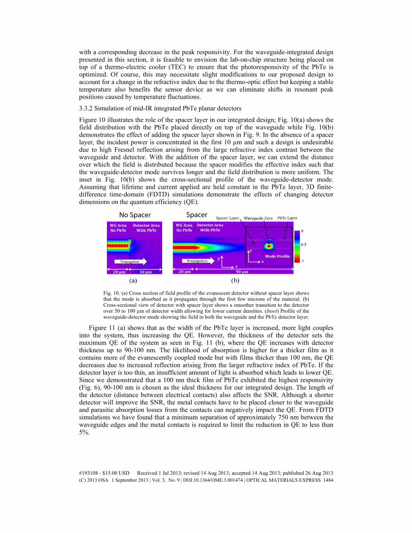
3.3.2 Simulation of mid-IR integrated PbTe planar detectors
Figure 10 illustrates the role of the spacer layer in our integrated design; Fig. 10(a) shows the field distribution with the PbTe placed directly on top of the waveguide while Fig. 10(b) demonstrates the effect of adding the spacer layer shown in Fig. 9. In the absence of a spacer layer, the incident power is concentrated in the first 10 µm and such a design is undesirable due to high Fresnel reflection arising from the large refractive index contrast between the waveguide and detector. With the addition of the spacer layer, we can extend the distance over which the field is distributed because the spacer modifies the effective index such that the waveguide-detector mode survives longer and the field distribution is more uniform. The inset in Fig. 10(b) shows the cross-sectional profile of the waveguide-detector mode. Assuming that lifetime and current applied are held constant in the PbTe layer, 3D finite-difference time-domain (FDTD) simulations demonstrate the effects of changing detector dimensions on the quantum efficiency (QE).
Fig. 10. (a) Cross section of field profile of the evanescent detector without spacer layer shows that the mode is absorbed as it propagates through the first few microns of the material. (b) Cross-sectional view of detector with spacer layer shows a smoother transition to the detector over 50 to 100 µm of detector width allowing for lower current densities. (Inset) Profile of the waveguide-detector mode showing the field in both the waveguide and the PbTe detector layer.
Figure 11 (a) shows that as the width of the PbTe layer is increased, more light couples into the system, thus increasing the QE. However, the thickness of the detector sets the maximum QE of the system as seen in Fig. 11 (b), where the QE increases with detector thickness up to 90-100 nm. The likelihood of absorption is higher for a thicker film as it contains more of the evanescently coupled mode but with films thicker than 100 nm, the QE decreases due to increased reflection arising from the larger refractive index of PbTe. If the detector layer is too thin, an insufficient amount of light is absorbed which leads to lower QE. Since we demonstrated that a 100 nm thick film of PbTe exhibited the highest responsivity (Fig. 6), 90-100 nm is chosen as the ideal thickness for our integrated design. The length of the detector (distance between electrical contacts) also affects the SNR. Although a shorter detector will improve the SNR, the metal contacts have to be placed closer to the waveguide and parasitic absorption losses from the contacts can negatively impact the QE. From FDTD simulations we have found that a minimum separation of approximately 750 nm between the waveguide edges and the metal contacts is required to limit the reduction in QE to less than 5%.
#193108 - $15.00 USD Received 1 Jul 2013; revised 14 Aug 2013; accepted 14 Aug 2013; published 26 Aug 2013(C) 2013 OSA 1 September 2013 | Vol. 3, No. 9 | DOI:10.1364/OME.3.001474 | OPTICAL MATERIALS EXPRESS 1484

Fig. 11. (a) The relation between QE and the detector width at various detector thicknesses shows higher QE with increasing detector width as more light couples into the system. (b) The relation between the QE and the detector thickness at various detector widths shows that increasing the detector thickness increases the QE as more of the propagating mode is contained in the detector layer. However, increasing the thickness beyond 90-100 nm increases the effective index to an extent that reduces QE.
Thus far, we have used a nominal refractive index of 1.5 for the spacer in our integrated detector simulations. To successfully translate the theoretical design to a working device, an appropriate spacer layer material has to be identified. The material has to meet the two key requirements of (a) transparency in the mid-IR and (b) ease of deposition. Given our target wavelengths in the 3–5 µm wavelength band, several commonly used polymers such as poly (methyl methacrylate – PMMA) which exhibit C-H bond absorption around 3.4 µm are unsuitable. Some that do meet the first criterion (e.g., Teflon) are hard to reliably deposit. Spin-coated fluorinated and deuterated polymers where the C-H bonds are replaced by C-F and C-D bonds respectively, present viable solutions as the absorption is pushed away from the 3.4 µm region [36, 37]. Inorganic compounds such as Al2O3 and alkali halides are also suitable materials due to their mid-IR transparency although the latter is harder to deposit. Although SiO2 has high absorption beyond λ = 3.5 µm, we can still use it as a spacer layer material for shorter wavelengths.
3.3.2 Fabrication of mid-IR integrated PbTe planar detectors
Fabrication of the integrated detector structure has relied on the demonstrated processing expertise in fabricating ChG-based waveguide and resonator structures as well as PbTe-based detectors. As shown in Fig. 12 the process flow for the detector begins with a pre-fabricated As2Se3 waveguide/resonator structure according to the scheme presented in H. Lin et al [38]. The first additional step is to deposit the spacer layer material, on which a layer of negative photoresist is coated for contact photolithography to define patterns for the PbTe detector layer. An alignment process ensures that the PbTe structures will be well-aligned to the waveguides underneath the spacer. Following the lithography, single-source thermal evaporation of PbTe and a lift-off process in acetone, removes the photoresist leaving behind only the required PbTe structures. A final photolithography step is performed for the metal contacts. As in the PbTe lithography step, an alignment procedure is required to ensure that the metal contacts are placed accurately on top of the PbTe structures. The metal contacts are deposited using electron beam evaporation followed by resist lift off in acetone (with ultrasonication). We used plasma-enhanced chemical vapor deposition (PECVD) to deposit SiO2 as the spacer layer for an initial target wavelength of 3.2 µm.
#193108 - $15.00 USD Received 1 Jul 2013; revised 14 Aug 2013; accepted 14 Aug 2013; published 26 Aug 2013(C) 2013 OSA 1 September 2013 | Vol. 3, No. 9 | DOI:10.1364/OME.3.001474 | OPTICAL MATERIALS EXPRESS 1485

Fig. 12. Process flow for the fabrication of a ChG waveguide-integrated PbTe detector.
Using our optimized design we successfully fabricated a prototype ChG waveguide-integrated PbTe detector (Fig. 13). Good alignment of the layers is seen with no post-fabrication discontinuities or cracks in either the metal or the underlying waveguide. The fully fabricated integrated detector structure is currently being tested to evaluate real world performance. The experimentally measured device performance will be compared with (a) the expected performance from simulations described above, as well as with (b) experimental measurements from thin photoconducting PbTe films at room temperature and at −60°C.
Fig. 13. (a) PbTe detector fabricated on an SiO2 spacer coated As2Se3 waveguide. (b) Final structure after fabrication of metal contacts shows good alignment and crack-free layers.
4. Conclusions
In conclusion, we demonstrate an integrated mid-IR microphotonics platform utilizing Si-CMOS compatible materials and fabrication processes. Using an engineered pedestal structure, our SOUP waveguide minimizes loss from the mid-IR absorptive silicon dioxide undercladding, and offers a 10 dB/cm improvement in optical loss for λ > 5 µm. The waveguide is crack-free with smooth sidewalls even after a multi-step dry/wet etching process, hence minimizing undesired scattering. Furthermore, a sharp fundamental mode is experimentally measured over a broad mid-IR regime. Finally, we introduce a monolithic ChGs waveguide-integrated PbTe thin film detector. The quantum efficiency of PbTe as a detector is optimized using appropriate thin film processing and geometry as well as by inserting a suitable spacer between the waveguide and PbTe layer. With the advantages of CMOS-process compatibility and on-chip mid-IR microphotonics, important applications such as portable and label free on-chip biochemical sensors are enabled.
Acknowledgments
Partial funding for this work has been provided by the US Department of Energy [Contract # DE-NA000421]. This paper has been pre-pared as an account of work partially supported by
#193108 - $15.00 USD Received 1 Jul 2013; revised 14 Aug 2013; accepted 14 Aug 2013; published 26 Aug 2013(C) 2013 OSA 1 September 2013 | Vol. 3, No. 9 | DOI:10.1364/OME.3.001474 | OPTICAL MATERIALS EXPRESS 1486

an agency of the United States Government. Neither the United States Government nor any agency thereof, nor any of their employees, makes any warranty, express or implied, or assumes any legal liability or responsibility for the accuracy, completeness or usefulness of any information, apparatus, product or process disclosed, or represents that its use would not infringe privately owned rights. Reference herein to any specific commercial product, process, or service by trade name, trademark, manufacturer, or otherwise does not necessarily constitute or imply its endorsement, recommendation, or favoring by the United States Government or any agency thereof. The views and opinions of authors expressed herein do not necessarily state or reflect those of the United States Government or any agency thereof.
#193108 - $15.00 USD Received 1 Jul 2013; revised 14 Aug 2013; accepted 14 Aug 2013; published 26 Aug 2013(C) 2013 OSA 1 September 2013 | Vol. 3, No. 9 | DOI:10.1364/OME.3.001474 | OPTICAL MATERIALS EXPRESS 1487


![Cumming [Mode de compatibilit ]) - Genopole Réussir en ...€“ By happy coincidence SiN is widely used passivation layer on CMOS © University of Glasgow, 2009 • CMOS-compatible](https://img.dokumen.tips/doc/110x75/5ac72ae97f8b9a42358b52b3/cumming-mode-de-compatibilit-genopole-russir-en-by-happy-coincidence.jpg)
![Broadband transparent and CMOS-compatible flat optics with ...Broadband transparent and CMOS-compatible flat optics with silicon nitride metasurfaces [Invited] SHANE COLBURN, 1,* ALAN](https://img.dokumen.tips/doc/110x75/5e36ae4ffc285e22940eb2f6/broadband-transparent-and-cmos-compatible-flat-optics-with-broadband-transparent.jpg)