Embed Size (px)
Citation preview

Sensors 2009, 9, 8336-8348; doi:10.3390/s91008336
sensors ISSN 1424-8220
www.mdpi.com/journal/sensors
Article
A CMOS-Compatible, Low-Noise ISFET Based on
High Efficiency Ion-Modulated Lateral-Bipolar Conduction
Sheng-Ren Chang and Hsin Chen *
Institute of Electronics Engineering, National Tsing Hua University, 30013 HsinChu, Taiwan;
E-Mail: [email protected] (S.-R.C)
* Author to whom correspondence should be addressed; E-Mail: [email protected];
Tel.: +886-3-5162221; Fax: +886-3-5162221.
Received: 30 July 2009; in revised form: 25 September 2009 / Accepted: 14 October 2009 /
Published: 21 October 2009
Abstract: Ion-sensitive, field-effect transistors (ISFET) have been useful biosensors in
many applications. However, the signal-to-noise ratio of the ISFET is limited by its intrinsic,
low-frequency noise. This paper presents an ISFET capable of utilizing lateral-bipolar
conduction to reduce low-frequency noise. With a particular layout design, the conduction
efficiency is further enhanced. Moreover, the ISFET is compatible with the standard CMOS
technology. All materials above the gate-oxide are removed by simple, die-level post-CMOS
process, allowing ions to modulate the lateral-bipolar current directly. By varying the
gate-to-bulk voltage, the operation mode of the ISFET is controlled effectively, so is the
noise performance measured and compared. Finally, the biasing conditions preferable for
different low-noise applications are identified. Under the identified biasing condition, the
signal-to-noise ratio of the ISFET as a pH sensor is proved to be improved by more than
five times.
Keywords: ISFET; low noise; CMOS-compatible; lateral-bipolar conduction
1. Introduction
Field-effect transistors have been employed as biosensors to detect ion concentration, biomolecules,
neural activity, etc. [1-6]. In these applications, a large sensor array is becoming essential for detecting
multiple biomolecules or for interfacing multiple biological cells in parallel [7-10]. This demand leads to
OPEN ACCESS
Sensors 2009, 9
8337
at least two challenges. First, integrating the sensors with signal-processing circuits on a single chip is
important to reduce wiring complexity and noise interferences. Second, the low-frequency noise of
field-effect sensors has to be further reduced for recording weak biomedical signals such as neural
activity, which could be less than tens of micro-volts in magnitude.
A variety of methods has been proposed to integrate field-effect sensors with the standard CMOS
technology [11-13], the prominent technology for fabricating integrated circuits. However,
micromachining processes become limited and only applicable after the CMOS process in a constrained
condition. To avoid complex post-CMOS processing, most CMOS-compatible, field-effect sensors
simply employ the passivation layer (silicon nitride/silicon oxynitride) as the surface material, and using
a floating gate formed by metals to couple the potential changes at the sensory surface [13-15].
Compared to the first ISFET with gate replaced by an aqueous solution [16], the floating-gate ISFET
requires a larger sensory area (several hundreds of m2) to ensure sufficient sensitivity. However,
applications like neural recording desire a pitch size smaller than a single neuron
(around 20 m) [6,17,18]. ISFETs with the discrete-gate structure [19,20], or the open-gate
structure [21,22], have thus been proposed. However, the open-gate structure in [22] is created by
plasma etching, which could damage the ISFET easily or introduce extra mismatches [23].
As most biomedical signals have a frequency bandwidth below 10 kHz [24], the low-frequency noise
of a field-effect transistor dominates to limit the signal-to-noise ratio of recording. One simple approach
is increasing the transistor size [25,26], but this again limits the minimum pitch size achievable. As
low-frequency noise is closely related to charge trapping at the oxide-silicon interface, the study in [27]
demonstrates that forward-biasing the source-to-bulk junction also helps to reduce low-frequency noise.
While such noise reduction could not be well explained by the models of the flicker noise [27,28], one
possible explanation is that the forward-biasing encourages the lateral-bipolar conduction, avoiding
interface traps and thus reducing noise [29,30]. However, the main drawback of the lateral-bipolar
conduction is the leakage current through the parasitic, vertical bipolar transistor (Figure 1).
Based on the post-CMOS process proposed in [23], this paper presents a CMOS-compatible ISFET
able to operate both in the metal-oxide-semiconductor (MOS) mode and in the lateral-bipolar junction
transistor (LBJT) mode. The LBJT conduction allows noise to be reduced significantly for low-noise
applications. The layout technique is further applied to define a particular structure, reducing the
leakage current of the bipolar conduction. In addition, all materials above the gate-oxide of the ISFET
are removed by the die-level, post-CMOS process, allowing the ions to modulate the drain current
directly, so as to enhance the sensitivity. Following the introduction, Section 2 describes the design,
fabrication, and the measurement setup of the ISFET. All the measurement results are presented and
discussed in Section 3. Finally, Section 4 concludes the findings and points out future works.
2. Experimental Section
2.1. The layout and the structure of the ISFET
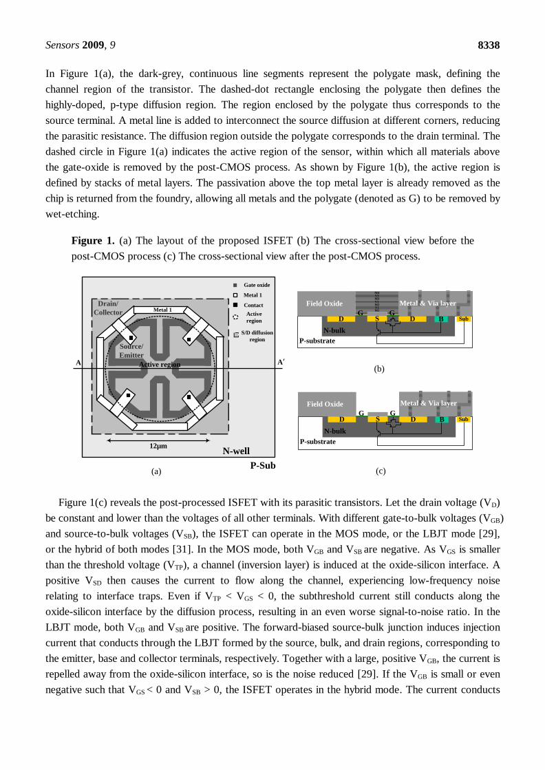
Figure 1(a) shows the layout of the ISFET for fabrication with the TSMC 0.35 m CMOS
technology. As the chip is returned from the foundry, the cross-sectional view along the line AA’ is
shown in Figure 1(b). The cross-sectional view then becomes Figure 1(c) after the post-CMOS process.
Sensors 2009, 9
8338
In Figure 1(a), the dark-grey, continuous line segments represent the polygate mask, defining the
channel region of the transistor. The dashed-dot rectangle enclosing the polygate then defines the
highly-doped, p-type diffusion region. The region enclosed by the polygate thus corresponds to the
source terminal. A metal line is added to interconnect the source diffusion at different corners, reducing
the parasitic resistance. The diffusion region outside the polygate corresponds to the drain terminal. The
dashed circle in Figure 1(a) indicates the active region of the sensor, within which all materials above
the gate-oxide is removed by the post-CMOS process. As shown by Figure 1(b), the active region is
defined by stacks of metal layers. The passivation above the top metal layer is already removed as the
chip is returned from the foundry, allowing all metals and the polygate (denoted as G) to be removed by
wet-etching.
Figure 1. (a) The layout of the proposed ISFET (b) The cross-sectional view before the
post-CMOS process (c) The cross-sectional view after the post-CMOS process.
Source/
Emitter
Drain/
Collector Metal 1
12µm
A A’Active region
Gate oxide
Metal 1
Contact
N-well
Active
region
S/D diffusion
region
P-Sub(a)
(b)
(c)
P-substrate
N-bulk
Field Oxide
D S
Metal & Via layer
BD SubGG
M4
M1V1M2V2M3V3
P-substrate
N-bulk
Field Oxide
D S
Metal & Via layer
BD SubGG
Figure 1(c) reveals the post-processed ISFET with its parasitic transistors. Let the drain voltage (VD)
be constant and lower than the voltages of all other terminals. With different gate-to-bulk voltages (VGB)
and source-to-bulk voltages (VSB), the ISFET can operate in the MOS mode, or the LBJT mode [29],
or the hybrid of both modes [31]. In the MOS mode, both VGB and VSB are negative. As VGS is smaller
than the threshold voltage (VTP), a channel (inversion layer) is induced at the oxide-silicon interface. A
positive VSD then causes the current to flow along the channel, experiencing low-frequency noise
relating to interface traps. Even if VTP < VGS < 0, the subthreshold current still conducts along the
oxide-silicon interface by the diffusion process, resulting in an even worse signal-to-noise ratio. In the
LBJT mode, both VGB and VSB are positive. The forward-biased source-bulk junction induces injection
current that conducts through the LBJT formed by the source, bulk, and drain regions, corresponding to
the emitter, base and collector terminals, respectively. Together with a large, positive VGB, the current is
repelled away from the oxide-silicon interface, so is the noise reduced [29]. If the VGB is small or even
negative such that VGS < 0 and VSB > 0, the ISFET operates in the hybrid mode. The current conducts

Sensors 2009, 9
8339
through both the MOS and the LBJT transistors. The proportion of the current in each transistor is
modulated by VGB, so is the noise.
The main drawback of the LBJT conduction is the unavoidable leakage current through the vertical
bipolar junction transistor (VBJT), which is always activated together with the LBJT. The leakage
current not only introduces extra power consumption but also puts the chip in the risk of latch-up. In
response to this drawback, our design has the source region completely surrounded by the drain region
(Figure 1(a)), enhancing the collection of hole currents for the LBJT. In addition, the polygonal
structure of the gate maximizes the W/L ratio (63 m/0.96 m), i.e., the emitter-base junction area of
the LBJT, within the finite active region. It is notable that the minimum channel length is not used in
order to ease the poly-gate etching.
Figure 2. (a) The chip containing the testkeys of the proposed ISFET; (b) The packaged
chip after post-CMOS process; (c) The schematic of the noise measurement system.
P-substrate
HP 4145
HP 35665A
PC (NoisePro)
Amplifier/Filters Unit
Connector A Connector B Noise Ouput
Controller Unit
VD
VS
VBULK
VG
Connector A Connector B
IEEE488
IEEE488
IEEE488
Cadence
9812B
N-bulk
D SOxide
D S Bulk GP-SUB
Battery
Ag/AgCl
electrode
Epoxy
(a)
(b) (c)
2.2. The post-CMOS process
The die-level, post-CMOS process for removing the materials in active region had been detailed and
carefully verified in [23]. The testkeys of the proposed ISFET were included in the chip shown in
Figure 2(a). The chip also contained multi-finger ISFET arrays integrated with recording amplifiers and
multiplexers, whose functionality had been tested and reported in [23,35]. After the chip was fabricated
with the standard CMOS process, the metal layers were first removed by wet etching with “piranha”
solution (H2SO4:H2O = 2:1) at 85 ºC for around 80 s until the polygate was exposed. The thin silicide
layer above the poly-gate was then removed by the reactive-ion etching (RIE) for five minutes.
Afterwards, the polygate was removed by wet etching with diluted KOH (KOH: DI water = 2:1 by
weight) at 80 ºC for around 20 seconds. With a shadow mask formed by a fragment of a silicon wafer,
Sensors 2009, 9
8340
the passivation layer above the bonding pads was removed by the RIE. The chip was then wire-bonded
to a printed circuit board, and the bonding wires were coated with the industrial epoxy (WK-8126H,
WinKing). Finally, a glass O-ring was attached to the PCB to form a tank for containing solutions above
the chip, as shown in Figure 2(b).
2.3. Noise Measurement
Figure 2(c) shows the measurement setup including a semiconductor parameter analyzer (HP 4145),
a dynamic signal analyzer (HP 35665A), and a noise analyzer (Cadence 9812B). The parameter analyzer
generated direct-current (DC) biases for the ISFET, and measuring the corresponding current or
voltage responses. Under different biasing conditions, the noise was first amplified by the noise analyzer,
and then measured by the dynamic signal analyzer. All the equipments were configured by the
software “NoisePro”.
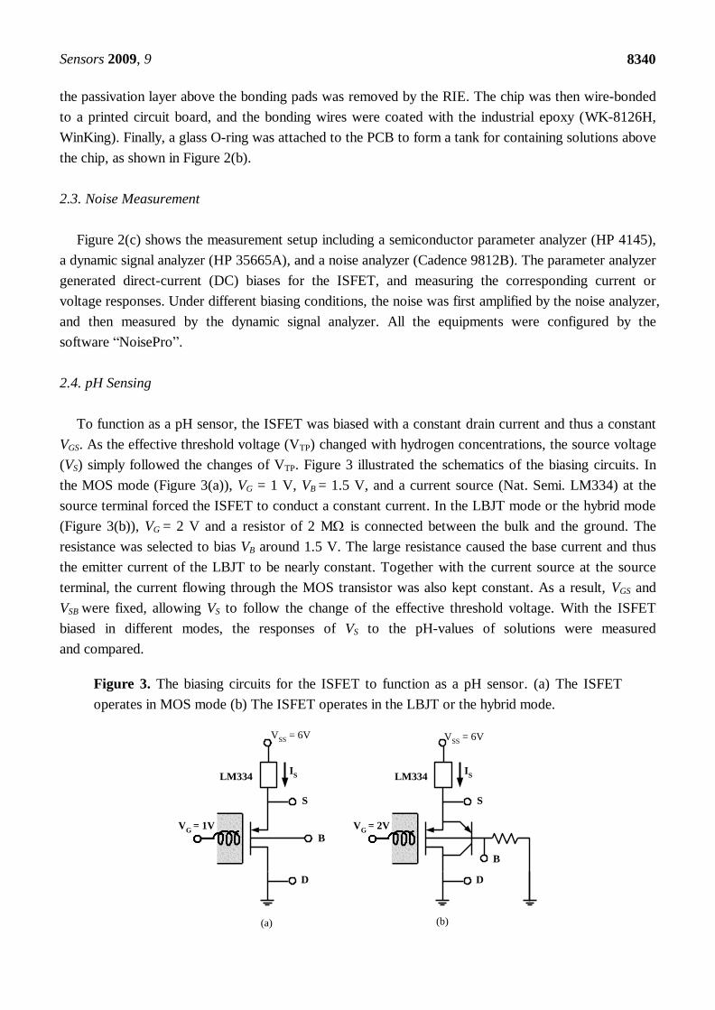
2.4. pH Sensing
To function as a pH sensor, the ISFET was biased with a constant drain current and thus a constant
VGS. As the effective threshold voltage (VTP) changed with hydrogen concentrations, the source voltage
(VS) simply followed the changes of VTP. Figure 3 illustrated the schematics of the biasing circuits. In
the MOS mode (Figure 3(a)), VG = 1 V, VB = 1.5 V, and a current source (Nat. Semi. LM334) at the
source terminal forced the ISFET to conduct a constant current. In the LBJT mode or the hybrid mode
(Figure 3(b)), VG = 2 V and a resistor of 2 M is connected between the bulk and the ground. The
resistance was selected to bias VB around 1.5 V. The large resistance caused the base current and thus
the emitter current of the LBJT to be nearly constant. Together with the current source at the source
terminal, the current flowing through the MOS transistor was also kept constant. As a result, VGS and
VSB were fixed, allowing VS to follow the change of the effective threshold voltage. With the ISFET
biased in different modes, the responses of VS to the pH-values of solutions were measured
and compared.
Figure 3. The biasing circuits for the ISFET to function as a pH sensor. (a) The ISFET
operates in MOS mode (b) The ISFET operates in the LBJT or the hybrid mode.
LM334I
S
S
B
VG
= 2V
D
LM334I
S
S
B
VG
= 1V
D
(a) (b)
VSS
= 6V VSS
= 6V

Sensors 2009, 9
8341
3. Results and Discussion
3.1. Device fabrication
Figure 4(a) shows a microphotograph of the ISFET, taken when the chip was just returned from the
foundry. The shining of the metals within the active region was clearly visible. After the post-CMOS
process, the shining disappeared completely, as shown in Figure 4(b), indicating the complete removal
of metal layers. The white line segments within the circle corresponded to the gate oxide of the ISFET,
and the light-red regions to the source diffusion covered by a thicker oxide. Although observing the
colors was not sufficient for confirming the complete removal of poly-gates, the duration of
KOH-etching has been optimized according to [23]. After the chip was packaged as Figure 2(b),
physiological buffer (210 mM NaCl; 15 mM CaCl2, 5.4 mM KCl, 2.6 mM MgCl2, and 5mM HEPES,
pH 7.4) was filled in the glass O-ring, and an Ag/AgCl wire was immersed in the buffer to define the
solution potential, i.e., the effective gate voltage of the ISFET.
Figure 4. (a) Sensor without post-CMOS process (b) Sensor after post-CMOS process.
3.2. Operation modes and efficiency
As the source voltage (VS) was swept from 1.0 V to 2.3 V with the solution potential (VG) stepping
from 0 V to 2.5 V with a stepsize of 25 mV, the drain current (ID) and the source current (IS) of the
ISFET were measured. The bulk and the drain voltages were kept constant (VB = 1.5 V, V D = 0 V)
during the measurement. Figure 5(a) plots ID against VSB for various VGB. The current-voltage
relationship was analogous to that measured from an ordinary LBJT with its gate remaining [29],
indicating that the gate-oxide of the ISFET had been successfully preserved from the post-CMOS
process. Moreover, Figure 5(a) revealed that the operation mode of the ISFET shifted from the MOS
mode to the LBJT mode as VGB increased from −0.9 V to 0.9 V. After VGB > 0.9 V, the ID-VSB curves
overlapped with the rightmost curve in Figure 5(a) because ID was entirely conducted through the LBJT.
Therefore, ions in the solution can only modulate ID effectively when VGB < 0.9 V, i.e., when the ISFET
operated in the MOS mode or the hybrid MOS-LBJT mode (VSB > 0).

Sensors 2009, 9
8342
Figure 5. (a) The measured ID-VSB characteristics of the ISFET for various VGB. (b) The
measured efficiency (ID/IS) against VGB of the ISFET when IS is fixed at 10 A. Operation
modes are changed from MOS mode to the LBJT mode by increasing the gate voltage.
-0.8 -0.4 0.0 0.4 0.8
0.65
0.70
0.75
0.80
0.85
0.90
0.95
1.00
ID/I
S
VGB
(v)
Efficiency
(a) (b)
-0.6 -0.4 -0.2 0.0 0.2 0.4 0.6 0.8
1E-6
1E-5
1E-4
ID(A)
VSB
(v)
Normal MOS BJT
S
D
G
B
VGB
= -0.9 to 0.9v
Let the efficiency of the ISFET be defined as the ratio between ID and IS. The efficiency is high when
the leakage current through the VBJT is small. Figure 5(b) plots the efficiency against VGB when IS is
fixed to be 10 A. The efficiency clearly depends on VGB, which determines the portion of ID conducting
through the LBJT. The efficiency is greater than 95% as VGB 0.5 V, and decreasing quickly to 65% as
VGB = 0.9 V. This indicates that LBJT conduction starts to dominate after VGB > 0.5 V, so is the leakage
current increased significantly. Nevertheless, by the merits of our layout design, the efficiency remains
more than 90% when 0 V < VGB < 0.6 V, within this range, the ISFET operates in the hybrid mode,
allowing ions to modulate ID with not only reduced noise but also high efficiency.
3.3. Transconductance
The transconductance (gm) of the ISFET is defined as the derivative of ID with respect to VGB. A
larger gm provides a better sensitivity to the potential changes within the solution. Figure 6(a) plots gm
against VGB with various VSB, revealing that gm decreases with increasing VGB. This is because positive
VGB repels the current away from the oxide-silicon interface, reducing the modulating capability of the
solution potential. With a specific VGB, the gm also decreases with increasing VSB because increasing VSB
forward-biases the source-bulk junction, causing more currents to flow through the LBJT. Figure 6(b)
further plots gm against ID for various VSB, showing clearly that a larger ID is required for achieving the
same gm as more current is conducted through the LBJT. Therefore, a compromise exists among the
noise, the efficiency, and the transconductance. If more current conducts through the LBJT, the noise is
smaller but the efficiency and the transconductance are degraded. The optimum biasing point for the
ISFET is thus application-dependent, as discussed in Sections 3.4 and 3.5.

Sensors 2009, 9
8343
Figure 6. The measured (a) gm-VGB (b) gm-ID of the ISFET for various VSB.
-1.0 -0.5 0.0 0.51E-7
1E-6
1E-5
1E-4
1E-3
gm(s)
VGB
(V)
VSB
= 0.8 V to -0.1V
VB=1.5v
1E-7 1E-6 1E-5 1E-41E-6
1E-5
1E-4
1E-3
gm(s)
ID(A)
VSB
=-0.1v
VSB
= 0.0v
VSB
= 0.1v
VSB
= 0.2v
VSB
= 0.3v
VSB
= 0.4v
VSB
= 0.5v
VSB
= 0.6v
VSB
= 0.7v
VSB
= 0.8v
VGB
= -1.5v to 1.0 v
VB=1.5v
(a) (b)
3.4. Noise performance with constant ID
As the ISFET is employed to detect ion concentration or biomolecules, the ISFET is normally biased
with a constant ID [32,33]. When ions or biomolecules change the effective threshold voltages, the
corresponding changes at VS are recorded. Since the voltage signal is recorded directly, the
transconductance of the ISFET is not of concern. The noise can thus be reduced by increasing VGB to
repel current conduction away from the oxide-silicon interface.
Figure 7. Noise measured with various VGB as the ISFET was biased with a constant ID.
(a) noise power spectral density (b) mean-square noise voltage integrated from 10
to 10 kHz
10 100 1000 10000
1E-21
1E-20
1E-19
1E-18
SI(A
2/H
z)
Frequency(Hz)
VGB= -1.5v
VGB= -1.0v
VGB= -0.5v
VGB=+0.0v
VGB=+0.1v
VGB=+0.2v
VGB=+0.3v
VGB=+0.4v
VGB=+0.5v
VGB=+0.6v
(a) (b)
-1.5 -1.0 -0.5 0.0 0.5
10-9
10-8
e
n
2(V
2)
VGB
(V)
Mean-square noise voltage
Figure 7(a) shows the noise spectrum measured as the ISFET is biased with ID = 10 A and various
VGB. The noise decreases by several decades as VGB increases from −1.5 V to 0.6 V. By integrating the
noise spectral over the frequency range of most biomedical signals (10–10 kHz) and dividing the
integrated value by gm2, the total mean-square noise voltage (en
2) referred to the sensory surface is
obtained and plotted in Figure 7(b). The noise reduces significantly after VGB > 0 V. Although the noise

Sensors 2009, 9
8344
continues to reduce with increasing VGB, the efficiency of the ISFET degrades after VGB > 0.5 V
(Figure 5(b)). Therefore, VGB = 0.5 V is a biasing point that achieves a good compromise between
efficiency and noise for the proposed ISFET.
3.5. Noise performance with constant gm
As the ISFET is employed to detect transient potential changes (e.g., neural activity), the potential
changes are normally transduced into drain currents for further amplification and filtering [34,35]. A
large transconductance (gm) is thus important for ensuring the sensitivity of the ISFET. As both noise
and gm decrease with VGB, an optimum VGB could exist for the hybrid-mode operation
(0 V < VGB < 0.6 V). Therefore, by biasing the ISFET with a constant gm = 0.1 mS, the noise spectral
density for various VGB is measured and shown in Figure 8(a).
Figure 8. Noise measured with various VGB as the ISFET was biased with a constant gm. (a)
noise power spectral density (b) mean-square noise current integrated from 10 to 10 kHz.
10 100 1000 10000
1E-19
1E-18 VGB=-0.25
VGB=0
VGB=0.1
VGB=0.2
VGB=0.3
SI(A
2/H
z)
Frequency(Hz)
VGB=-1.5
VGB=-1.25
VGB=-1
VGB=-0.75
VGB=-0.5
(a) (b)
-1.6 -1.2 -0.8 -0.4 0.0 0.4
3.5x10⁻¹⁶
4.0x10⁻¹⁶
4.5x10⁻¹⁶
5.0x10⁻¹⁶
in
2(A
2)
VGB
(V)
Mean-square noise current
The total mean-square noise current (in2) integrated from 10 to 10 kHz is shown in Figure 8(b),
where the error bars represent the standard errors across two devices. For VGB < −0.8 V, MOS
conduction in the saturation mode dominates. In this operating mode, the same ID gives the same gm. As
the low-frequency noise is simply proportional to ID [28], the noise power is roughly the same for
different VGB. As −0.8 V < VGB < 0 V, the MOS enters the substhreshold operation. Increasing VGB
causes interface traps to be more negatively-charged, and thus easier to attract hole currents to induce
noise [20]. Most important of all, as VGB > 0 V, the operation shifts into the hybrid mode. A minimum
occurs at VGB = 0.2 V. As discussed in Section 3.3, the minimum comes from the fact that increasing
VGB encourages LBJT conduction to reduce noise while causing gm to reduce at the same time. A higher
VGB thus requires a higher biasing current to maintain gm = 0.1 mS, but the noise increases with the
biasing current. Therefore, the biasing point at VGB = 0.2 V achieves a good compromise between the
transconductance and the noise. Beyond this point, the increase of noise with the biasing current
becomes non-negligible. Although a local optimum point exists for the hybrid operation, the noise level
in the hybrid mode is not significantly lower than that in the MOS mode. The only difference is that the
noise in the MOS mode exhibits larger variation, owing to the fact that the noise is closely related to the

Sensors 2009, 9
8345
interface traps, whose amount varies easily from one device to another. In addition, the noise reduction
in the hybrid mode is much less significant than that achieved in the constant-ID case (Figure 7(b)).
Therefore, to use the ISFET as a potentiometric sensor, biasing the ISFET as a source follower as
shown in Figure 3(b) is still preferable.
3.6. pH sensing
Section 3.4 indicated that the ISFET with VGB = 0.5 achieved a good compromise between high
efficiency and small noise. To verify the noise reduction improved the signal-to-noise ratio, the
sensitivity of the ISFET operating in different modes was further measured and compared in the context
of pH sensing. The red circles in Figure 9 showed the measured responses of VS as the ISFET was
biased in the MOS mode with VGB = −0.5 V (Figure 3(a)). On the other hand, the black squares showed
the responses of VS as the ISFET was biased in the hybrid mode with VGB = 0.5 V (Figure 3(b)). The
error bars indicated the standard deviation over four measurements. By fitting the results with the red
and black lines, the sensitivity was found to be 26 mV/pH for the MOS mode and 20 mV/pH for the
hybrid mode. As the mean-square noise voltage with VGB = −0.5 was around 35 times larger than that
with VGB = 0.5 (Figure 7(b)), it is clear that the hybrid mode improves the signal-to-noise ratio by
around five times.
Figure 9. The measured responses of VS to solutions with different pH values as the ISFET
was biased in the MOS mode (red) and in the hybrid mode (black).
4 6 8 10 12
-0.08
-0.04
0.00
0.04
0.08
26mV/PH
20mV/PH
Hybrid mode
MOS mode
V
S(V
)
PH
4. Conclusions
A CMOS-compatible ISFET capable of operating in both MOS and LBJT modes has been fabricated
and tested. The special structure defined by layout masks is proved to facilitate operation in the hybrid
MOS-LBJT mode with high efficiency and low noise. With constant-current biasing, the noise of the
ISFET can be reduced by two decades by adjusting the gate-to-bulk voltage (VGB). As transconductance
is of concern, an optimum VGB exists for the ISFET to have sufficient transconductance, high efficiency,
and minimized noise. As the ISFET can be fabricated by simple post-CMOS process at the die level, the
Sensors 2009, 9
8346
ISFET will be integrated with signal-processing circuits on a single chip for low-noise,
biomedical applications.
Acknowledgements
The authors would like to express their thanks to the National Science Council in Taiwan and the
Brain Research Center in the National Tsing Hua University for funding this project (NSC grant code:
NSC 96-2627-E-007-002) and to the National Chip Implementation Center in Taiwan for the chip
fabrication.
References and Notes
1. Bergveld, P. Thirty years of ISFETOLOGY What happened in the past 30 years and what may
happen in the next 30 years. Sens. Actuat. B: Chem. 2003, 88, 1–20.
2. Kim, D.S.; Jeong, Y.T.; Park, H.J.; Shin, J.K.; Choi, P.; Lee, J.H.; Lim, G. An FET-type charge
sensor for highly sensitive detection of DNA sequence. Biosens. Bioelectron. 2004, 20, 69–74.
3. Dzyadevych, S.V.; Soldatkin, A.P.; El’skaya, A.V.; Martelet, C. Enzyme biosensors based on ion-
selective field-effect transistors. Anal. Chim. Acta 2006, 568, 248–258.
4. Fromherz, P.; Carsten, O.; Weis, R. Neuron transistor: Electrical transfer function measured by the
patch-clamp technique. Phys. Rev. Lett. 1993, 71, 4079–4082.
5. Fromherz, P. and Offenhausser, A. A neuron-silicon junction: A Retzius cell of the leech on an
insulated-gate field-effect transistor. Science 1990, 252, 1290–1293.
6. Hutzler, M.; Fromherz, P. Silicon chip with capacitors and transistors for interfacing organotypic
brain slice of rat hippocampus. Eur. J. Neurosci. 2004, 19, 2231–2238.
7. Milgrew, M.J.; Riehle, M.O.; Cumming, D.R.S. A large transistor-based sensor array chip for
direct extracellular imaging. Sens. Actuat. B 2005, 111, 347–353.
8. Hizawa, T.; Sawada, K.; Takao, H.; Ishida, M. Fabrication of a two-dimensional ph image sensor
using a charge transfer technique. Sens. Actuat. B 2006, 117, 509–515.
9. Eversmann, B.; Jenkner, M.; Hofmann, F.; Paulus, C.; Brederlow, R.; Holzap, B.; Fromherz, P.;
Merz, M.; Steinhauser, M.M.; Eckstein, G; Schmitt-Landsiedel, D.; Thewes, R. A 128 × 128
CMOS biosensor array for extracellular recording of neural activity. IEEE J. Solid-State Circ.
2003, 38, 2306–2317.
10. Parak, W.J.; George, M.; Gaub, H.E. Bohm, S.; Lorke, A. The field-effect-addressable
potentiometric sensor/stimulator (FAPS)Xa new concept for a surface potential sensor and
stimulator with spatial resolution. Sens. Actuat. B: Chem. 1999, 58, 497–504.
11. Hierlemann, A.; Baltes, H. CMOS-based chemical microsensors. Analyst 2003, 128, 15–28.
12. Joo, S.; Brown, R.B. Chemical sensors with integrated electronics. Chem. Rev. 2008, 108,
638–651.
13. Bausells, J.; Carrabina, J.; Errachid, A.; Merlos, A. Ion-sensitive field-effect transistors fabricated
in a commercial cmos technology. Sens. Actuat. B 1999, 57, 56–62.
14. Hammond, P.A.; Ali, D.; Cumming, D.R.S. Design of a single-chip ph sensor using a conventional
0.6μm CMOS process. IEEE Sens. J. 2004, 4, 706–712.

Sensors 2009, 9
8347
15. Hammond, P.A.; Ali, D.; Cumming, D.R.S. A system-on-chip digital ph meter for use in a wireless
diagnostic capsule. IEEE Trans. Biomed. Eng. 2005, 52, 687–694.
16. Bergveld, P. Development, operation, and application of the ion-sensitive field-effect transistor as
tool for electrophysiology. IEEE Trans. Biom. Eng. 1972, BME-19, 342–351.
17. Eversmann, B.; Jenkner, M.; Hofmann, F.; Paulus, C.; Brederlow, R.; Holzapfl, B.; Fromherz, P.;
Merz, M.; Brenner, M.; Schreiter, M.; Gabl, R.; Plehnert, K.; Steinhauser, M.; Eckstein, G.;
Schmitt-Landsiedel, D.; Thewes, R. A 128 × 128 CMOS biosensor array for extracellular
recordingof neural activity. IEEE J. Solid-State Circ. 2003, 38, 2306–2317 .
18. Lambacher, A.; Jenkner, M.; Merz, M.; Eversmann, B.; Kaul, R.A.; Hofmann, F.; Thewes, R.;
Fromherz, P. Electrical imaging of neuronal activity by multi-transistor-array (MTA) recording at
7.8μm resolution. Appl. Phys. A-Mater. Sci. Process. 2004, 79, 1607–1611.
19. Chin, Y.L.; Chou, J.C.; Sun, T.P.; Chung, W.Y.; Hsiung, S.K. A novel ph sensitive isfet with on-
chip temperature sensing using CMOS standard process. Sens. Actuat. B 2001, 76, 582–593.
20. Chin, Y.L.; Chou, J.C.; Sun, T.P.; Liao, H.K.; Chung, W.Y.; Hsiung, S.K. A novel SnO2/Al
discrete gate ISFET ph sensor with CMOS standard process. Sens. Actuat. B 2001, 75, 36–42.
21. Lauwers, E.; Suls, J.; Gumbrecht, W.; Maes, D.; Gielen,G.; Sansen, W. A CMOS multiparameter
biochemical microsensor with temperature control and signal interfacing. IEEE J. Solid-state Circ.
2001, 36, 2030–2038.
22. Witvrouw, A.; Steenkiste, F.V.; Maes, D.; Haspeslagh, L.; Gerwen, P.V.; Moor, P.D.; Sedky, S.;
Hoof, C.V.; Vries, A.C. Verbist, A.; Caussemaeker, A.D.; Parmentier, B. Baert, K. Why CMOS-
integrated transducers? A review. Microsyst. Technol. 2000, 6, 192–199.
23. Chang, S.R. Die-level, post-CMOS processes for fabricating open-gate, field-effect biosensor
arrays with on-chip circuitry. J. Micromech. Microeng. 2008, 18, 115032.
24. Harrison, R.R. A versatile integrated circuit for the acquisition of biopotentials. In Proceedings of
IEEE Custom Integrated Circuits Conference, San Jose, CA, USA, September 16–19, 2007;
pp. 115–122.
25. Deen, M.J.; Levinshtein, M.E.; Rumyantsev, S.L.; Orchard-Webb, J. Generation-recombination
noise in MOSFETs. Semicond. Sci. Technol. 1999, 14, 298–304.
26. Phillip, E.A.; Douglas, R.H. CMOS Analog circuit Design, 2nd Ed.; Oxford University: New York,
NY, USA, 2002; pp. 408–409.
27. Deen, M.J.; Marinov, O. Effect of forward and reverse substrate biasing on low-frequency noise in
silicon PMOSFETs. IEEE Trans. Electron Dev. 2002, 49, 409–413.
28. Vandamme, L.K.J.; Li, X.; Rigaud, D. 1/f noise in MOS devices, mobility or number fluctuations?
IEEE Trans. Electron Dev. 1994, 41, 1936–1945.
29. Vittoz, E.A.; MOS transistors operated in the lateral bipolar mode and their application in CMOS
technology. IEEE J. Solid-State Circ. 1983, 18, 273–279.
30. Holman, W.T.; Connelly, J.A. A compact low noise operational amplifier for a 1.2 μm digital
CMOS technology. IEEE J. Solid-State Circ. 1995, 30, 710–714.
31. MacSweeney, D.; McCarthy, K.G.; Mathewson, A.; Mason, B.; A SPICE compatible subcircuit
model for lateral bipolar transistors in a CMOS process. IEEE Trans. Electron Dev. 1998,
45, 1978–1984.
Sensors 2009, 9
8348
32. Chung, W.Y.; Yang, C.H.; Pijanowska, D.G.; Grabiec, P.B.; Torbicz, W. ISFET performance
enhancement by using the improved circuit techniques. Sens. Actuat. B: Chem. 2006, 113,
555–562.
33. Bousse, L.; Shott, J.; Meindl, J.D. A process for the combined fabrication of ion sensors and
CMOS circuits. IEEE Electron Dev. Lett. 1988, 9, 44–46.
34. Chang, C.H.; Chang, S.R.; Lin, J.S.; Lee, Y.T.; Yeh, S.R.; Chen, H. A CMOS neuroelectronic
interface based on two-dimensional transistor arrays with monolithically-integrated circuitry.
Biosens. Bioelectron. 2009, 24, 1757–1764.
© 2009 by the authors; licensee Molecular Diversity Preservation International, Basel, Switzerland. This
article is an open-access article distributed under the terms and conditions of the Creative Commons
Attribution license (http://creativecommons.org/licenses/by/3.0/).


![Broadband transparent and CMOS-compatible flat optics with ...Broadband transparent and CMOS-compatible flat optics with silicon nitride metasurfaces [Invited] SHANE COLBURN, 1,* ALAN](https://img.dokumen.tips/doc/110x75/5e36ae4ffc285e22940eb2f6/broadband-transparent-and-cmos-compatible-flat-optics-with-broadband-transparent.jpg)