Embed Size (px)
Citation preview

INSTITUTE OF PHYSICS PUBLISHING JOURNAL OF MICROMECHANICS AND MICROENGINEERING
J. Micromech. Microeng. 15 (2005) 336–345 doi:10.1088/0960-1317/15/2/013
A CMOS-compatible high aspectratio silicon-on-glass in-planemicro-accelerometerJunseok Chae, Haluk Kulah and Khalil Najafi
Department of Electrical Engineering and Computer Science, The University of Michigan,Ann Arbor, MI 48109-2122, USA
E-mail: [email protected]
Received 29 June 2004, in final form 20 October 2004Published 24 November 2004Online at stacks.iop.org/JMM/15/336
AbstractThis paper presents a post-CMOS-compatible micro-machinedsilicon-on-glass (SOG) in-plane capacitive accelerometer. Theaccelerometer is a high aspect ratio structure with a 120 µm thicksingle-crystal silicon proof-mass and 3.4 µm sense gap, bonded to a glasssubstrate. It is fabricated using a simple 3-mask, 5-step process, and is fullyCMOS compatible. A CMOS switched-capacitor readout circuit and anoversampled �–� modulator are used to read out capacitance changes fromthe accelerometer. The CMOS chip is 2.6 × 2.4 mm2 in size, utilizeschopper stabilization and correlated double sampling techniques, has a106 dB open-loop dynamic range, a low input offset of 370 µV, and canresolve better than 20 aF. The accelerometer system has a measuredsensitivity of 40 mV g−1 and input referred noise density of 79 µg Hz−1/2.Using the SOG configuration, a post-CMOS monolithic integrationtechnique is developed. The integration technique utilizes dielectric bridges,silicon islands and the SOG configuration to obtain a simple, robust andpost-CMOS-compatible process. Utilizing this technique, an integratedSOG accelerometer has been fabricated using the University of Michigan3 µm CMOS process.
1. Introduction
High precision micro-accelerometers are increasinglyneeded in applications such as inertial navigation,seismology and micro-gravity measurements [1]. Capacitivemicro-accelerometers have several advantages such as highsensitivity, stable dc-characteristics, low drift, low powerdissipation and low-temperature sensitivity. One of theimportant requirements for accelerometers is high resolution[2]. Many out-of-plane (z-axis) micro-accelerometers whichprovide micro-g resolution have been developed [3–6]. Inorder to reduce noise and increase sensitivity, these sensorsutilize full wafer thickness or multiple bonded wafers toform a large proof-mass, and a thin sacrificial layer toform the sense gap. However, it is not practical to easilyemploy these techniques in in-plane (x- or y-axis) sensorsthat are sensitive to acceleration parallel to the sensorsubstrate.
Surface-micro-machined accelerometers can beintegrated with interface electronics to improveperformance. However, due to their small mass they typicallyhave a noise floor of 0.03–1 mg Hz−1/2 [7–9]. In orderto overcome this limit, bulk micro-machined or SOI (silicon-on-insulator) accelerometers utilizing DRIE (deep reactiveion etching) technology have been developed [10, 11]. Theseaccelerometers utilize 25–70 µm thick single-crystal siliconproof-mass to reduce overall system noise. Nevertheless,these accelerometers either do not provide high enoughresolution to satisfy an inertial grade performance or have acomplicated fabrication process and large parasitics. In thispaper, we report a post-CMOS-compatible high aspect ratiolow-noise, high-sensitivity in-plane accelerometer, with asimple fabrication process, which is interfaced with acustom-designed switched-capacitor readout circuit. In thefollowing sections, the structure of the accelerometer anddesign procedure including sensor performance optimization
0960-1317/05/020336+10$30.00 © 2005 IOP Publishing Ltd Printed in the UK 336
A CMOS-compatible high aspect ratio silicon-on-glass in-plane micro-accelerometer
Table 1. SOG accelerometer design parameters for performance optimization.
Parameters Range Weight
Mechanical dimensions Length/width ratio of proof-mass 1.2–20 − −Length and width of sense finger 0.2–1 (mm) and 10–25 (µm) −Die size 1–5 (mm2) +
Physical characteristics Quality factor 0.05–0.1 − −Cross-axis sensitivity < −60 (dB) +Shock resistance > 1000 (g) + +Operating range > ±1 (g) + +
Electrical properties Cut-off frequency >100 (Hz) +Pull-in voltage >3 (V) +Sense capacitance >10 (pF) + +Stability (n · kele/kspring) >50 + + +
Figure 1. SOG in-plane accelerometer.
are presented first. Micro-machined accelerometer fabricationand associated process issues follow. Then, measurementresults of the accelerometer system with CMOS readoutcircuitry are presented. Finally, we demonstrate a post-CMOSmonolithic integration technique using dielectric bridges,silicon islands and SOG configuration [12–14] to obtain asingle-chip monolithic accelerometer system.
2. Sensor design
Figure 1 illustrates the SOG in-plane accelerometer structure.The accelerometer has a 120 µm thick proof-mass suspendedover a glass substrate. This structure is simple and utilizes thewell-known lateral combs for sense and force feedback, exceptthat it has a large proof-mass and sense capacitance because ofits large thickness and the small sense gap realized by DRIE.
2.1. Design parameter optimization
In order to achieve high sensitivity and low-noise performance,a target object function is defined as (sensitivity/mechanicalnoise),
Sensitivity
Mechanical Noise∝
√Lelectrode
Helectrode
n
k2 · d0· M2 (1)
where n is the number of sense electrodes, k is the springconstant, M is the mass of proof-mass, d0 is the sense gap,Lelectrode and Helectrode are the length and height of an electrode,respectively [13, 15].
The initial design target for mechanical noise density is10 µg Hz−1/2. The thickness of the proof-mass is 120 µm,
Table 2. SOG accelerometer design parameters.
Mass of the proof-mass 0.5 mgResonant frequency 2.14 kHzThickness of the proof-mass 120 µmSense gap 2.0 µmSense capacitance 32.1 pFSpring constant of spring beams 90.4 N m−1
Cross-axis sensitivity <0.1%
Sensitivity/mechanical noise (0.78 pF g−1)/(10 µg Hz−1/2)
but it could be made thicker. The target object function isoptimized with different design variables to obtain a highperformance accelerometer, listed in table 1. In orderto perform an efficient optimization process, a customizedweight function has been assigned to each parameter to avoidunnecessary trivial minor adjustments. Among the dependentparameters, stability is assigned to be the most significantfactor, so as to ensure a stable closed-loop operation.n · kele/kspring is a measure of stability (kele is the springconstant of an electrode and kspring is the spring constantof spring beams attached to the proof-mass). This ratio isdesigned to be larger than 50 to achieve a stable closed-loopoperation [16].
Figure 2 shows two three-dimensional (3D) plots of theoptimization. The plots illustrate how high sensitivity can beobtained using a mechanical noise of 10 µg Hz−1/2 device.Table 2 summarizes the optimized design parameters. Notethat the mass of the proof-mass is close to a milligram, whichis an order of magnitude higher than that of surface-micro-machined devices. Also, sense capacitance is substantialenough to improve immunity to parasitic capacitances, whichenables hybrid assembly with readout electronics.
2.2. Sensor system noise
High sensitivity and low noise are most essential since theydetermine the input referred noise density (IRND), often calledthe noise floor. In an accelerometer system, IRND is derivedfrom two components—system gain and output system noisedensity (OSND):
System gain (V g−1) = (Sensitivity of device)
× (Sensitivity of readout circuitry)
OSND (V Hz−1/2)
=√
(Nmechanical × System gain)2 + N2electronic
337

J Chae et al
Figure 2. Design parameter optimization.
(where Nmechanical and Nelectronic denote mechanical andelectronic noise, respectively).
The system gain consists of sensitivities of theaccelerometer and the readout circuit. The output system noisedensity is the addition of noise powers from the mechanicalpart, multiplied by the system gain, and the electronic part.Note that the noise density indicates not just mechanicalnoise, but the accelerometer system noise. In this paper,noise represents the overall system noise unless it is statedas mechanical or electronic noise. IRND can be expressed as
IRND (g Hz−1/2) = OSND (V Hz−1/2)/System gain (V g−1)
=√
N2mechanical +
(Nelectronic
System gain
)2
.
Assuming a signal-to-noise ratio (SNR) of 1, the resolution,sometimes called the minimum detectable signal, of the sensoris defined as the multiplication of IRND and the measurementbandwidth. Since the bandwidth is an application-specificparameter, IRND is, generally, the measure of resolution.
To estimate the resolution of the SOG accelerometersystem, the contribution from readout electronic noise needsto be taken into account. If we assume a circuit sensitivityof 0.3 V pF−1, a sensor sensitivity of 0.78 pF g−1, and a totaloutput electronic noise of 25 µV over a 100 Hz BW [17], theIRND of the SOG accelerometer system can be estimated as
IRND =
√√√√(10 µg Hz−1/2)2 +
(25 µV/
√100 Hz
0.78 pF g−1 × 0.3 V pF−1/2
)2
= 14.6 µg Hz−1/2.
Note that the noise density is strongly dependent on thesystem gain, which is itself dependent on both device andcircuit sensitivities. Since electronic noise increases ascircuit sensitivity increases, in order to have a low-noiseaccelerometer system, it is preferred to use a high-sensitivityand low-noise accelerometer structure.
2.3. FEM verification
Optimized design parameters are verified using FEMsimulation. Figure 3 shows the resonant frequencies of theSOG accelerometer. As seen, the first mode (y-axis) resonantfrequency is 2.14 kHz, giving a spring constant of 93.5 N m−1.The resonant frequencies for the second and third modes are14.6 kHz (z-axis) and 22.9 kHz (x-axis) respectively. Theseare much higher than the first mode, resulting in low cross-axis sensitivity. Sensitivity to off-axis acceleration is alsoverified by FEM simulation. By definition of sensitivity of any
X
YZX
YZX
YZX
YZ
1st mode 2nd mode 3rd mode
Figure 3. Resonant frequencies of the SOG accelerometer.
Table 3. Cross-axis sensitivities.
�x/�y �z/�y �C/C
x-axis 0.26% 0.02% −98.88 dBz-axis 0.008% 2.2% −67.15 dB
Note that y is the sense axis.
parameter to a second parameter, cross-axis sensitivities aredetermined by equation (2) (note that y is the sense axis), andshown in table 3. Cross-axis sensitivities for x- and z-axes areestimated as −99 dB and −67 dB, respectively. The x-axiscross-axis sensitivity is much lower than the z-axis due to thelarger spring constant:
S�C�ax,z
= �C/C
�ax,z/ax,z
. (2)
Shock resistance is also simulated to evaluate if the device isrobust enough to sustain external unexpected shocks. For thesense axis (y-axis), the proof-mass movement is constrainedby shock stops, thus the sense structures can be protected.For x- and z-axes, a 1000g external shock is simulated. Themaximum stresses occur at the edge of the spring beams, andare 10.4 MPa for the x-axis shock and 98.6 MPa for the z-axisshock, respectively. This shows that the sensor should be ableto survive under a 1000g shock since the fracture strength forsingle-crystal silicon is at least 600 MPa [18].
3. Fabrication
The fabrication process has only five steps, requiring threemasks as shown in figure 4. The process is simple, requires nospecial steps other than DRIE, and does not require any high-temperature processing, which is favorable for post-CMOSprocessing. The glass substrate bonded to the single-crystalsilicon is insulating, which reduces parasitics and therebyfacilitates interfacing with a hybrid readout circuit.
First, a glass substrate with a shallow recess is preparedfor anodic bonding (a). Then, a standard silicon wafer (withCMOS circuitry if needed) is anodically bonded to the glass
338

A CMOS-compatible high aspect ratio silicon-on-glass in-plane micro-accelerometer
(a)
(c)
(b)
(e)
(d )
Figure 4. Fabrication sequence.
Proof-mass
Sense Fingers
Suspension Beams
Anchors
Shock-Stop
Figure 5. Top view of fabricated SOG accelerometer and shockstop.
substrate (b). The silicon wafer is then thinned to 120 µm usingstandard chemical mechanical polishing (CMP) (c). After theCMP step, the metal contacts (Cr/Au) are evaporated andpatterned. Finally, the wafer is DRIE etched to define theproof-mass and sense fingers. Figure 5 shows SEM views ofthe SOG accelerometer, 2.2 × 3.0 × 0.12 mm3 in size, and ashock stop for preventing excessive proof-mass movement toprotect sense fingers from an external shock. There are twocritical steps influencing the overall performance; DRIE etchand micro-loading effect. Detailed description and methodsto minimize these influences are discussed in the followingsubsections.
3.1. DRIE technology
DRIE technology is crucial for the SOG accelerometer since itdoes not only release the device but also determines the sensegap distance. The sense gap is the most important parameteraffecting squeeze film damping and sensitivity. The SOGaccelerometer is designed to have a 2 µm gap and a depth of120 µm (60:1 ratio). The etch profile needs to be carefullycharacterized since a non-vertical sidewall profile introducesnon-linearity [19]. To obtain a 60:1 aspect ratio, the pressureinside the etch chamber is initially high and is reduced as theetch proceeds, which helps to remove etch by-products fromthe deep trench. DRIE etch parameters are listed in table 4.Figure 6 shows a vertical etch profile and sense gap after
~ 100µm
Sense Gap
Figure 6. Vertical etch profile of sense fingers and sense gap after70 min DRIE etch.
Table 4. DRIE etch parameters.
Coil/platenTime (s) Flow rate (sccm) power (W)
Etch 12 SF6/O2 (130/13) 80/10Passivation 6 C4F8 (85) 80/0Pressure Automatic pressure control, 65–0.6%/min
70 min DRIE. Although the sense gap is designed to be 2 µm,it becomes wider due to the finite lateral etch during the highaspect ratio etch. This reduces device sensitivity because thesensitivity is proportional to d0
−2.
3.2. Micro-loading effect
The micro-loading effect becomes significant when etchingtwo different width trenches side-by-side [20]. Obviously,SOG devices have different size trenches, which make themvulnerable to this effect. Figure 7 illustrates the micro-loadingeffect. As the DRIE etch proceeds, a wide trench is etchedfaster than a narrow trench due to different etch rates. Oncethe etching of the wide trench is complete, positive ions reachthe bottom of silicon through the wide trench, get chargedup on the glass substrate, and attack silicon from the bottomside, which results in a thinner structure [21]. The proof-mass from the device is taken and placed upside down toobserve the micro-loading effect after finishing the DRIE etch(∼80 min), as is shown in figure 8. Note that the roughnessof the sense fingers is due to the non-directional etch fromthe bottom of silicon through the wide trench. The crosssections of the proof-mass and sense fingers are also shownin figure 8. The thickness of the sense fingers is 100 µminstead of 120 µm, which results in a 20% sensitivity reductiondue to the loss of sense area. Moreover, the vertical etchprofile is compromised due to the micro-loading effect, whichintroduces non-linearity.
In order to prevent etching from the backside, a shieldingmetal layer is placed between the thinned silicon and the glasssubstrate. In so doing, both silicon and glass have the sameelectrical potential, which prevents charging up the dielectricsubstrate [21]. As a result, sense fingers maintain their original
339
J Chae et al
Silicon
Glass
Different size of trenches
Start attacking the bottom
Figure 7. Micro-loading effect [21].
Proof-massSenseFingers
SenseFingers Proof-mass
120µm100µm
SenseFingers Proof-mass
120µm100µm
Figure 8. Micro-loading effect on the fabricated SOGaccelerometer.
15µm
10µm
Metal layerMetal layer
(a)
(b)
Figure 9. Method to avoid the micro-loading effect: (a) damagedsense finger and (b) sense finger with an electrical short path.
height and near ideal vertical sidewall profile as shown infigure 9.
4. Test results
4.1. Electrostatic measurement
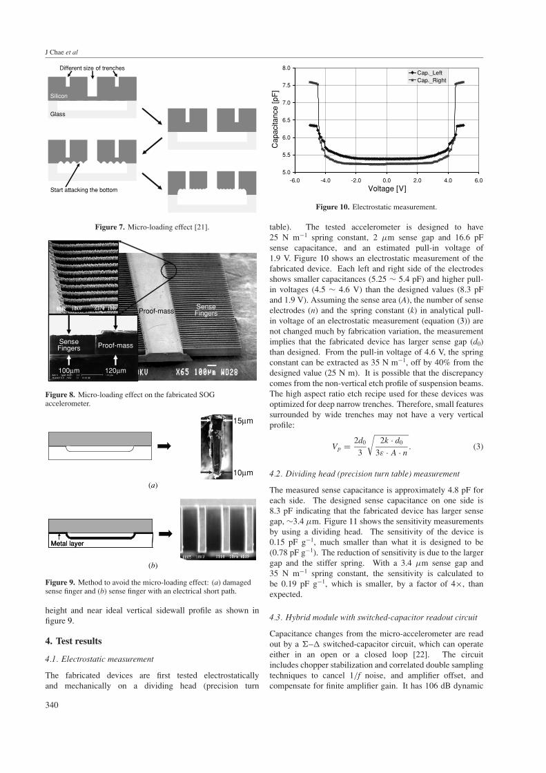
The fabricated devices are first tested electrostaticallyand mechanically on a dividing head (precision turn
5.0
5.5
6.0
6.5
7.0
7.5
8.0
-6.0 -4.0 -2.0 0.0 2.0 4.0 6.0
Voltage [V]
Cap
acita
nce
[pF
]
Cap._LeftCap._Right
Figure 10. Electrostatic measurement.
table). The tested accelerometer is designed to have25 N m−1 spring constant, 2 µm sense gap and 16.6 pFsense capacitance, and an estimated pull-in voltage of1.9 V. Figure 10 shows an electrostatic measurement of thefabricated device. Each left and right side of the electrodesshows smaller capacitances (5.25 ∼ 5.4 pF) and higher pull-in voltages (4.5 ∼ 4.6 V) than the designed values (8.3 pFand 1.9 V). Assuming the sense area (A), the number of senseelectrodes (n) and the spring constant (k) in analytical pull-in voltage of an electrostatic measurement (equation (3)) arenot changed much by fabrication variation, the measurementimplies that the fabricated device has larger sense gap (d0)than designed. From the pull-in voltage of 4.6 V, the springconstant can be extracted as 35 N m−1, off by 40% from thedesigned value (25 N m). It is possible that the discrepancycomes from the non-vertical etch profile of suspension beams.The high aspect ratio etch recipe used for these devices wasoptimized for deep narrow trenches. Therefore, small featuressurrounded by wide trenches may not have a very verticalprofile:
Vp = 2d0
3
√2k · d0
3ε · A · n. (3)
4.2. Dividing head (precision turn table) measurement
The measured sense capacitance is approximately 4.8 pF foreach side. The designed sense capacitance on one side is8.3 pF indicating that the fabricated device has larger sensegap, ∼3.4 µm. Figure 11 shows the sensitivity measurementsby using a dividing head. The sensitivity of the device is0.15 pF g−1, much smaller than what it is designed to be(0.78 pF g−1). The reduction of sensitivity is due to the largergap and the stiffer spring. With a 3.4 µm sense gap and35 N m−1 spring constant, the sensitivity is calculated tobe 0.19 pF g−1, which is smaller, by a factor of 4×, thanexpected.
4.3. Hybrid module with switched-capacitor readout circuit
Capacitance changes from the micro-accelerometer are readout by a �–� switched-capacitor circuit, which can operateeither in an open or a closed loop [22]. The circuitincludes chopper stabilization and correlated double samplingtechniques to cancel 1/f noise, and amplifier offset, andcompensate for finite amplifier gain. It has 106 dB dynamic
340

A CMOS-compatible high aspect ratio silicon-on-glass in-plane micro-accelerometer
y = 0.152x - 0.136R2 = 0.989
-0.3
-0.25
-0.2
-0.15
-0.1
-0.05
0
-1 -0.5 0 0.5 1Input Acceleration [g]
Diff
eren
tial C
apac
itanc
e [p
F]
Figure 11. Sensitivity measurement using a dividing head.
range, an offset of 370 µV and can resolve better than20 aF. Figure 12 shows the simplified schematics of theCMOS capacitive interface chip and its hybrid connectionto the sensor. Two fixed external reference capacitors areused to establish a full-bridge scheme. The hybrid systemis assembled onto a PC board and mounted in a standard24-pin IC package as shown in figure 12. Note that of thesix devices on a die, only one is connected to the circuit fortesting.
The hybrid system is tested for sensitivity and noise floorin an open-loop configuration. The open-loop test is performedon a dividing head, in a 1g gravitational field, by changing theacceleration from −1g to +1g. Figure 13 shows the open-looptest result for the hybrid system, indicating a sensitivity of∼40 mV g−1. This result matches with the expected valuesince the device has a sensitivity of ∼0.15 pF g−1 and thereadout circuit has a voltage gain of 300 mV pF−1.
The noise density of the SOG accelerometer system canbe estimated as (note that the mechanical noise is reduced to4.5 µg Hz−1/2 due to the enlarged sense gap):
Figure 12. Hybrid accelerometer and readout electronics system in IC package.
y = 38.641x + 16.719R2 = 0.986
-20
0
20
40
60
-0.8 -0.4 0 0.4 0.8Input Acceleration [g]
Diff
eren
tial O
utpu
t [m
V]
Figure 13. Open-loop test result of the hybrid system.
IRND =
√√√√(4.5 µg Hz−1/2)2 +
(25 µV/
√100 Hz
40 mV g−1
)2
= 82.6 µg Hz−1/2.
The measured output noise spectrum of the system (obtainedusing a dynamic signal analyzer HP3561) is shown in figure 14.The total noise over a bandwidth of 100 Hz is ∼22.4 µV,which indicates that the noise density of the current hybridsystem is
IRND =√
2 × 22.4 µV
40 mV g−1
/√100 Hz = 79.1 µg Hz−1/2.
The√
2 term is added to account for the two output channelsof the circuit. As is observed, the calculated output systemnoise floor matches well with the measured value.
The measured system noise floor of 79.1 µg Hz−1/2 is highbecause of the small gain of the hybrid module (40 mV g−1)and the low sensitivity of the accelerometer. Table 5
341

J Chae et al
Figure 14. Output spectrum of the hybrid system.
Table 5. Hybrid sensor/circuit module specifications.
MEMS device parametersSensitivity 0.15 pF g−1
Mechanical noise 4.51 µg Hz−1/2
Interface readout circuitry parametersSampling clock 30 kHzPower dissipation <6.6 mW @ 5 VCapacitance sensitivity 0.3 V pF−1
Resolution <20 aFOffset 2.7 mV (370 µV w/chopper
stabilization)
MEMS device and interface circuitry moduleSensitivity 40 mV g−1
Open-loop noise density 79.1 µg Hz−1/2
summarizes accelerometer-interface circuit hybrid modulespecifications. Table 6 shows the estimated and measuredsensitivity, noise floor and the sensitivity/noise ratio of thisaccelerometer, and compares these values to those of otherdevices reported in the literature.
5. CMOS compatibility
Surface micro-machining technology has been usedextensively for industrial MEMS accelerometer products[23, 24]. One of the biggest advantages of surface micro-machining technology is easy monolithic integration withelectronics to achieve small size and improve performance.However, surface-micro-machined devices often do not satisfythe requirements of high performance applications. In order
Table 6. Sensitivity/noise ratio.
SOG
ADXL [7] UCB [9] CMU [31] IMI [11] Estimated Measured
Sensitivity (fF g−1) 0.1 4.5 0.3 102 780 150Noise Floor (µg Hz−1/2) 225 32 50 25 14.6 79.1Sensitivity/noise floor 0.0004 0.14 0.006 4.1 53 1.9
ADXL stands for Analog Device Inc.’s; UCB stands for University of California at Berkeley; CMUstands for Carnegie Mellon University; IMI stands for Integrated Micro-Instruments.
to meet these requirements, devices fabricated using SOI orbulk micro-machining utilizing wafer bonding technologieshave been developed [11, 13, 25–27]. The silicon-on-glass(SOG) device, presented in this paper, is one of them.Although these devices offer higher sensitivity and lowernoise floor than surface-micro-machined devices, monolithiccircuit integration with these devices is a challenge. This isbecause the sensors often require additional steps before orafter standard circuit fabrication process.
We propose a standard post-CMOS monolithic fabricationtechnique utilizing the SOG configuration. This techniqueuses dielectric bridges, silicon islands and the SOGconfiguration to obtain simple, robust and a fully CMOS-compatible MEMS integration process.
5.1. Post-CMOS fabrication
Depending on where the additional steps to build MEMSdevices are performed with respect to circuit fabrication, theprocesses are referred to as pre-CMOS, pre-and-post CMOS[11, 28] and post-CMOS [29]. The post-CMOS technique hasbeen the most popular because it is the most reliable, simpleand inexpensive although it is limited to low-temperatureprocess steps to prevent any damage to electronics alreadyfabricated on the wafer [10, 29].
The post-CMOS technique has a few requirements. Firstof all, as mentioned above, the process steps after circuitfabrication must be performed at low temperature. Second,the interconnection scheme between MEMS devices and theelectronics should be robust enough to survive when MEMSdevices move. Finally, the additional manufacturing stepsafter circuit fabrication should be simple because as the post-CMOS fabrication becomes more complicated, the overallyield decreases, and the manufacturing cost increases.
5.2. A monolithic integration technique using SOGconfiguration
The SOG configuration is a low-temperature process andhas simple fabrication steps. In order to obtain robustinterconnections, as introduced in the previous section,dielectric bridges and silicon islands are developed andcombined with the SOG configuration. Figure 15 illustratesthe monolithic integration scheme. A glass substrate supportselectrically isolated pieces of silicon defined by DRIE. A metallayer is used for interconnection lines. Although the thicknessof silicon is chosen as 120 µm in this work, it can be thickerup to full wafer thickness. It is determined by the capabilityof DRIE, which is limited only by the required aspect ratio ofMEMS structures.
342

A CMOS-compatible high aspect ratio silicon-on-glass in-plane micro-accelerometer
IC
Silicon Islands
Interconnectionlines
Glass substrate
120µmFig.16
Figure 15. SOG monolithic integration scheme.
Figure 16 shows the structure of the dielectric bridgecarrying signals between silicon islands. The metalinterconnection goes over the silicon islands with the helpof the dielectric bridge. The dielectric bridge consists of anumber of layers such as thick field oxide and CVD oxideprovided by the CMOS fabrication steps. Output pads forconnecting to external power supplies, VDD and ground, or fortesting and sensor output are formed on the top of the siliconislands.
The SOG monolithic integration process is shown infigure 17. The process is quite similar to the SOGaccelerometer presented previously. First, conventional ICfabrication is performed on a silicon wafer. A glass substratewith a recess and a shielding metal is also prepared. The metalis deposited and patterned on the glass substrate not only toavoid the micro-loading effect from the following DRIE, butalso to protect the IC from the large electric field during thebonding process. Next, the fabricated silicon IC wafer isanodically bonded to the glass substrate, and is thinned tothe desired thickness using CMP. Finally, metal contacts areformed, and DRIE is used to define the MEMS structure,silicon islands and dielectric bridges.
(a)
(c)
(b)
(d )
Figure 17. Fabrication sequence of SOG monolithic integration: (a) standard CMOS process on a silicon wafer, (b) a glass substrate withshielding metal, (c) flip the silicon wafer & bond to the glass substrate and CMP the silicon wafer and (d ) deposit contact metal & DRIE.
Silicon Islands
DielectricBridge
InterconnectionLines
GlassRecess
GlassSubstrate
Silicon Islands
InterconnectionLines
DielectricBridge
Via
Figure 16. Dielectric bridge and silicon islands.
An integrated SOG accelerometer has been fabricatedusing the University of Michigan 3 µm 2-poly 1-metal CMOSprocess [30]. Figure 18 shows an optical photograph of aMEMS device integrated with readout electronics before post-CMOS MEMS fabrication steps. Reference capacitors forfull-bridge operation, metal interconnections and connectionto silicon islands are fabricated on a standard silicon wafer.Figure 19 shows the fabricated chip after the post-CMOS steps,including anodic bonding, CMP, contact metal deposition andDRIE. Each metal pad on top of silicon islands is electricallyisolated from the other, and is used to connect to the outsideworld. Close-up views of the silicon islands, dielectric bridgesand interconnection are shown in figure 20.
5.3. Test results
The threshold voltages of nMOS and pMOS transistors weremeasured to be 0.74 V and 0.49 V, respectively (figure 21).Obviously, the positive pMOS threshold voltage is not whatwas expected, and results in malfunction of the entire readoutcircuit. We do not know why the pMOS transistor’s thresholdvoltage was off the target, but nMOS was right on the target.This is likely due to some contamination or a problem in ionimplantation.
343

J Chae et al
ME
MS
Device
CM
OS
Circuitry
ReferenceCapacitors
MetalInterconnections
Connectionsto Silicon Islands
Figure 18. Fabricated integrated MEMS device with readoutelectronics.
SOGAccelerometers
CMOS electronicsunderneath
Bondpads
Figure 19. Fabricated chip after post-CMOS process.
Although MEMS devices integrated with CMOS circuitwere not realized successfully, the core elements of theintegration process have been successfully demonstrated. Ithas been shown that a standard CMOS wafer can be bonded toglass, polished back, and DRIE etched to form MEMS devices.The dielectric bridge and silicon islands are successfullyfabricated and enable signal routing and transfer between thecircuits and MEMS devices. The problem associated with thethreshold voltage of pMOS transistors can be solved by usingstandard CMOS wafers from a commercial foundry.
6. Conclusion
In this paper, a fully CMOS-compatible high aspect ratiosilicon-on-glass (SOG) configuration micro-accelerometerwith CMOS readout circuitry is presented. The SOGconfiguration uses a high aspect ratio structure with 120 µmthick single-crystal silicon proof-mass and 3.4 µm sense gap,bonded to a glass substrate. The accelerometer has a simple
Silicon Islands
Pad
Comb fingers bondedto the glass substrate
(Silicon Islands)
Glass recess
Dielectric bridge
Interconnection
Via holes50µm
(a)
(b)
Figure 20. Silicon islands, dielectric bridge and interconnection:(a) silicon islands and pad and (b) interconnection between combfingers.
y = 6.584x - 4.858
0
5
10
15
0 0.5 1 1.5 2 2.5 3
VGS [V]
SQ
RT
(ID
) [m
A]
SQ
RT
(ID
) [m
A]
y = -5.096x + 2.510
0
5
10
15
-2 -1.5 -1 -0.5 0 0.5VGS [V]
(a) nMOS
(b) pMOS
Figure 21. Transistor V GS versus ID characteristics.
3-mask, 5-step process, and is fully CMOS compatible. Targetsensitivity and noise floor of the SOG accelerometer withreadout circuitry are 0.78 pF g−1 and 15 µg Hz−1/2.
A CMOS switched-capacitor front-end circuit is usedto read out the capacitance changes from the micro-accelerometer. The circuit has a 106 dB open-loop dynamic
344

A CMOS-compatible high aspect ratio silicon-on-glass in-plane micro-accelerometer
range, a low input offset of 370 µV and can resolve betterthan 20 aF. A hybrid microsystem consisting of the SOGaccelerometer and �–� switched-capacitor readout circuitprovides a measured sensitivity of 0.15 pF g−1 and a noisefloor of 79 µg Hz−1/2. The sensitivity reduction is mostlyfrom an enlarged sense gap due to the finite lateral DRIE etch.
A monolithic post-CMOS integration technique utilizingdielectric bridges, silicon islands and SOG configurationhas been developed. This technique is simple, robust andfully post-CMOS compatible. A glass substrate supports thesilicon islands and signal routing is provided with the help ofthe dielectric bridge between the silicon islands. Utilizingthis technique, an integrated SOG accelerometer has beenfabricated using the University of Michigan 3 µm CMOSprocess.
Acknowledgments
The authors would like to thank Junmo Kang, Arvind Salianand the staff at WIMS, University of Michigan. This workhas been supported by DARPA under contract no F30602-98-2-0231. This work made use of the WIMS EngineeringResearch Center’s Shared Facilities supported by the NationalScience Foundation under award no EEC-0096866.
References
[1] Yazdi N, Ayazi F and Najafi K 1998 Micro-Machined inertialsensors Proc. IEEE 86 1640–58
[2] I S 1293-1998 1999 IEEE standard specification format guide,test procedure for linear, single-axis, nongyroscopicaccelerometers
[3] I O Inc. 2003 Si-Flex 1500-ULND Evaluation Board, SingleChannel Digital Output
[4] Rudolf F, Jornod A, Bergqvist J and Leuthold H 1990Precision accelerometers with µg resolution SensorsActuators A 21 297–302
[5] Chae J, Kulah H and Najafi K 2003 A monolithic three-axissilicon capacitive accelerometer with micro-g resolutionTransducers ’03: Proc. 12th Int. Conf. on Solid-StateSensors and Actuators (Boston, MA) pp 81–4
[6] Kulah H, Chae J and Najafi K 2003 Noise analysis andcharacterization of a sigma-delta capacitive siliconmicro-accelerometer Transducers ’03: Proc. 12th Int. Conf.on Solid-State Sensors and Actuators (Boston, MA) pp 95–8
[7] Analog-Devices 1999 ADXL105, High accuracy ±1g to ±5gsingle axis iMEMS accelerometer with analog input
[8] Lu C, Lemkin M and Boser B E 1995 Monolithic surfacemicro-machined accelerometer with digital output IEEEJ. Solid-State Circuits 30 1367–73
[9] Jiang X, Wang F, Kraft M and Boser B 2002 An integratedsurface micro-machined capacitive lateral accelerometerwith 2µg/
√Hz resolution Proc. Hilton Head Islands
pp 202–5[10] Xiao Z, Wu G, Chen M, Zhao C, Zhang D, Hao Y and Li Z
1999 Laterally capacity sensed accelerometer fabricatedwith the anodic bonding and the high aspect ratio etchingTransducers ’99: Proc. 10th Int. Conf. on Solid-StateSensors and Actuators (Sendai) pp 1518–21
[11] Lemkin M, Juneau T, Clark W, Roessig T and Brosnihan T1999 A low-noise digital accelerometer using integratedSOI-MEMS technology Transducers ’99: Proc. 10th Int.Conf. on Solid-State Sensors and Actuators (Sendai)pp 1294–7
[12] Iliescu C and Miao J 2003 One-mask process for siliconaccelerometers on Pyrex glass utilising notching effect ininductively coupled plasma DRIE Electron. Lett. 39 658–9
[13] Chae J, Kulah H and Najafi K 2002 A hybrid silicon-on-glass(SOG) lateral micro-accelerometer with CMOS readoutcircuitry MEMS ’02: Proc. 15th IEEE Int. Conf. onMicro Electro Mechanical Systems (Las Vegas, NV)pp 623–6
[14] Hein S, Holzner K, Schlichting V, Obermeier E and Barton K1997 Capacitive differential pressure sensor with highoverload capability using silicon/glass technologyTransducers ’97: Proc. Int. Conf. on Solid State Sensorsand Actuators (Chicago) vol 2 pp 1477–80
[15] Chae J, Kulah H and Najafi K 2004 An in-planehigh-sensitivity, low-noise micro-g silicon accelerometerwith CMOS readout circuitry J. Microelectromech. Syst. 13628–35
[16] Yazdi N 1999 Micro-g silicon accelerometers with highperformance CMOS interface circuitry DoctoralDissertation EECS, The University of Michigan, Ann Arbor
[17] Kulah H, Salian A, Yazdi N and Najafi K 2002 A 5v closed-loop second-order sigma-delta micro-g micro accelerometerProc. Hilton Head Islands pp 219–22
[18] Yi T, Li L and Kim C-J 2000 Microscale material testing ofsingle crystalline silicon: Process effects on surfacemorphology and tensile strength Sensors Actuators A 83172–8
[19] Ramos J 1997 Sensitivity enhancement in lateral capacitiveaccelerometers by structure width optimization Electron.Lett. 33 384–6
[20] Kuehl K, Vogel S, Schaber U, Schafflik R and Hillerich B1998 Advanced silicon trench etching in MEMSapplications Proc. SPIE 3511 97–105
[21] Chabloz M, Jiao J, Yoshida Y, Matsuura T and Tsutsumi K2000 Method to evade microloading effect in deep reactiveion etching for anodically bonded glass–silicon structuresMEMS ’00: Proc. 13th IEEE Int. Conf. on Micro ElectroMechanical Systems (Miyazaki) pp 283–7
[22] Yazdi N and Najafi K 1999 Interface IC for a capacitivesilicon µg accelerometer ISSCC ’99: Proc. IEEE Int. SolidState Circuits Conference (San Francisco, CA)pp 132–3
[23] Analog-Devices 1996 ADXL50, monolithic accelerometerwith signal conditioning, data sheet
[24] Cross-bow 2001 High sensitivity accelerometer, LF series datasheet
[25] Ishihara K, Yung CF, Ayon A A and Schmidt M A 1999Inertial sensor technology using DRIE and wafer bondingwith interconnecting capability J. Microelectromech. Syst. 8403–8
[26] Smith T, Nys O, Chevroulet M, DeCoulon Y and Degrauwe M1994 A 15 b electromechanical sigma-delta converter foracceleration measurements ISSCC ’94: Proc. IEEE Int.Solid-State Circuits Conference (San Francisco, CA)pp 160–1
[27] Yazdi N and Najafi K 2000 All-silicon single-wafer micro-gaccelerometer with a combined surface and bulkmicromachining process J. Microelectromech. Syst. 9544–50
[28] Parameswaran L, Hsu C and Schmidt M A 1995 MergedMEMS-CMOS process using silicon wafer bondingTechnical Digest International Electron Devices Meetingpp 613–6
[29] Xie H, Erdmann L, Zhu X, Gabriel K J and Fedder G K 2000Post-CMOS processing for high-aspect-ratio integratedsilicon microstructures Proc. Solid-State Sensors andActuators Workshop (Hilton Head Island, SC) pp 77–80
[30] Cho S T and Ji J 1992 CMOS integrated circuits and siliconmicromachining Thesis EECS, The University of Michigan,Ann Arbor
[31] Wu J and Carley L R 2002 A low-noise low-offsetchopper-stabilized capacitive readout amplifier for CMOSMEMS accelerometers ISSCC ’02: Proc. IEEE Int. SolidState Circuits Conference (San Francisco, CA)pp 428–9
345