Embed Size (px)
Citation preview
Section 3. Memory Organization
Mem
ory
Org
anizatio
n
3
HIGHLIGHTS
This section of the manual contains the following topics:
3.1 Introduction................................................................................................................3-2
3.2 Control Registers....................................................................................................... 3-2
3.3 Memory Layout........................................................................................................ 3-12
3.4 Address Map ........................................................................................................... 3-14
3.5 Bus Matrix................................................................................................................ 3-27
3.6 I/O Pin Control ......................................................................................................... 3-31
3.7 Operation in Power-Saving and Debug Modes ....................................................... 3-31
3.8 Code Examples ....................................................................................................... 3-31
3.9 Related Application Notes ....................................................................................... 3-32
3.10 Revision History....................................................................................................... 3-33
© 2007-2015 Microchip Technology Inc. DS60001115H-page 3-1

PIC32 Family Reference Manual
3.1 INTRODUCTION
The PIC32 microcontrollers provide 4 GB of unified virtual memory address space. All memoryregions, including program memory, data memory, SFRs and Configuration registers reside inthis address space at their respective unique addresses. The program and data memories canbe optionally partitioned into user and kernel memories. In addition, the data memory can bemade executable, allowing the PIC32 to execute from data memory.
Key features of PIC32 memory organization include the following:
• 32-bit native data width
• Separate User and Kernel mode address spaces
• Flexible program Flash memory partitioning
• Flexible data RAM partitioning for data and program space
• Separate boot Flash memory for protected code
• Robust bus-exception handling to intercept runaway code
• Simple memory mapping with Fixed Mapping Translation (FMT) unit
• Cacheable and non-cacheable address regions
3.2 CONTROL REGISTERS
This section lists the Special Function Registers (SFRs) used for setting the RAM and Flashmemory partitions for data and code (for both User and Kernel mode).
• BMXCON: Bus Matrix Configuration Register
This register configures program Flash cacheability for DMA accesses, bus errorexceptions, data RAM wait states and arbitration modes.
• BMXDKPBA: Data RAM Kernel Program Base Address Register, BMXDUDBA: Data RAM User Data Base Address Register, BMXDUPBA: Data RAM User Program Base Address Register, and BMXPUPBA: Program Flash Memory User Program Base Address Register
These registers identify relative base addresses for kernel, User mode data and User modeprogram space in RAM.
• BMXDRMSZ: Data RAM Size Register
This read-only register identifies the size of the Data RAM in bytes.
• BMXPFMSZ: Program Flash Memory Size Register
This read-only register identifies the size of the Program Flash Memory in bytes.
• BMXDRMSZ: Data RAM Size Register
This read-only register identifies the size of the Boot Program Flash Memory in bytes.
Note: This family reference manual section is meant to serve as a complement to devicedata sheets. Depending on the device variant, this manual section may not apply toall PIC32 devices.
Please consult the note at the beginning of the “Memory Organization” chapter inthe current device data sheet to check whether this document supports the deviceyou are using.
Device data sheets and family reference manual sections are available fordownload from the Microchip Worldwide Web site at: http://www.microchip.com
DS60001115H-page 3-2 © 2007-2015 Microchip Technology Inc.

© 2007-2015 M
icrochip Technolo
gy Inc.
DS
60001115H
-page 3-3
Sectio
n 3. M
emo
ry Org
anizatio
n
Ta fter the summary, which include detailedde
Ta
20/4 Bit 19/3 Bit 118/2 Bit 17/1 Bit 16/0
BM MXRIXI
BMXERRICD
BMXERRDMA
BMXERRDS
BMXERRIS
— BMXARB<2:0>
BM — — — BMXDKPBA<16>
BM — — — BMXDUDBA<16>
BM — — — BMXDUPBA<16>
BM
BM BMXPUPBA<19:16>
BM
BM
LeNo name with CLR, SET, or INV appended to the end of
r. Reads from these registers should be ignored.
Memory Organization 3
ble 3-1 provides a brief summary of all related Memory organization registers. Corresponding register tables appear ascription of each register bit.
ble 3-1: Memory Organization SFR Summary
NameBit
RangeBit 31/15 Bit 30/14 Bit 29/13 Bit 28/12 Bit 27/11 Bit 26/10 Bit 25/9 Bit 24/8 Bit 23/7 Bit 22/6 Bit 21/5 Bit
XCON(1)31:16 — — — — —
BMXCHEDMA
— — — — —B
ER
15:0 — — — — — — — — —BMX
WSDRM— —
XDKPBA(1) 31:16 — — — — — — — — — — — —
15:0 BMXDKPBA<15:0>
XDUDBA(1) 31:16 — — — — — — — — — — — —
15:0 BMXDUDBA<15:0>
XDUPBA(1) 31:16 — — — — — — — — — — — —
15:0 BMXDUPBA<15:0>
XDRMSZ 31:16 BMXDRMSZ<31:16>
15:0 BMXDRMSZ<15:0>
XPUPBA(1) 31:16 — — — — — — — — — — — —
15:0 BMXPUPBA<15:0>
XPFMSZ 31:16 BMXPFMSZ<31:16>
15:0 BMXPFMSZ<16:0>
XBOOTSZ 31:16 BMXBOOTSZ<31:16>
15:0 BMXBOOTSZ<15:0>
gend: — = unimplemented, read as ‘0’. Address offset values are shown in hexadecimal.te 1: This register has an associated Clear, Set, and Invert register at an offset of 0x4, 0x8, and 0xC bytes, respectively. These registers have the same
the register name (e.g., BMXCONCLR). Writing a ‘1’ to any bit position in these registers will clear, set, or invert valid bits in the associated registe

PIC32 Family Reference Manual
Register 3-1: BMXCON: Bus Matrix Configuration Register
Bit Range
Bit31/23/15/7
Bit30/22/14/6
Bit29/21/13/5
Bit28/20/12/4
Bit27/19/11/3
Bit26/18/10/2
Bit25/17/9/1
Bit24/16/8/0
31:24U-0 U-0 U-0 U-0 U-0 R/W-0 U-0 U-0
— — — — —BMX
CHEDMA(1) — —
23:16U-0 U-0 U-0 R/W-1 R/W-1 R/W-1 R/W-1 R/W-1
— — —BMX
ERRIXIBMX
ERRICDBMX
ERRDMABMX
ERRDSBMX
ERRIS
15:8U-0 U-0 U-0 U-0 U-0 U-0 U-0 U-0
— — — — — — — —
7:0U-0 R/W-1 U-0 U-0 U-0 R/W-0 R/W-0 R/W-1
—BMX
WSDRM— — — BMXARB<2:0>
Legend:
R = Readable bit W = Writable bit U = Unimplemented bit, read as ‘0’
-n = Value at POR ‘1’ = Bit is set ‘0’ = Bit is cleared x = Bit is unknown
bit 31-27 Unimplemented: Read as ‘0’
bit 26 BMXCHEDMA: BMX PFM Cacheability for DMA Accesses bit(1)
1 = Enable program Flash memory (data) cacheability for DMA accesses (requires cache to have data caching enabled)
0 = Disable program Flash memory (data) cacheability for DMA accesses (hits are still read from the cache, but misses do not update the cache)
bit 25-21 Unimplemented: Read as ‘0’
bit 20 BMXERRIXI: Enable Bus Error from IXI bit
1 = Enable bus error exceptions for unmapped address accesses initiated from IXI shared bus0 = Disable bus error exceptions for unmapped address accesses initiated from IXI shared bus
bit 19 BMXERRICD: Enable Bus Error from ICD Debug Unit bit
1 = Enable bus error exceptions for unmapped address accesses initiated from ICD0 = Disable bus error exceptions for unmapped address accesses initiated from ICD
bit 18 BMXERRDMA: Bus Error from DMA bit
1 = Enable bus error exceptions for unmapped address accesses initiated from DMA0 = Disable bus error exceptions for unmapped address accesses initiated from DMA
bit 17 BMXERRDS: Bus Error from CPU Data Access bit (disabled in Debug mode)
1 = Enable bus error exceptions for unmapped address accesses initiated from CPU data access0 = Disable bus error exceptions for unmapped address accesses initiated from CPU data access
bit 16 BMXERRIS: Bus Error from CPU Instruction Access bit (disabled in Debug mode)
1 = Enable bus error exceptions for unmapped address accesses initiated from CPU instruction access0 = Disable bus error exceptions for unmapped address accesses initiated from CPU instruction access
bit 15-7 Unimplemented: Read as ‘0’
bit 6 BMXWSDRM: CPU Instruction or Data Access from Data RAM Wait State bit
1 = Data RAM accesses from CPU have one wait state for address setup0 = Data RAM accesses from CPU have zero wait states for address setup
bit 5-3 Unimplemented: Read as ‘0’
Note 1: This bit is not available on all devices. Refer to the “Memory Organization” chapter in the specific device data sheet to determine availability.
DS60001115H-page 3-4 © 2007-2015 Microchip Technology Inc.

Section 3. Memory OrganizationM
emo
ry
Org
anizatio
n
3
bit 2-0 BMXARB<2:0>: Bus Matrix Arbitration Mode bits
111 = Reserved; do not use. Using these Configuration modes will produce undefined behavior•••
011 = Reserved; do not use. Using these Configuration modes will produce undefined behavior.010 = Arbitration Mode 2001 = Arbitration Mode 1 (default)000 = Arbitration Mode 0
Register 3-1: BMXCON: Bus Matrix Configuration Register (Continued)
Note 1: This bit is not available on all devices. Refer to the “Memory Organization” chapter in the specific device data sheet to determine availability.
© 2007-2015 Microchip Technology Inc. DS60001115H-page 3-5

PIC32 Family Reference Manual
Register 3-2: BMXDKPBA: Data RAM Kernel Program Base Address Register
Bit Range
Bit31/23/15/7
Bit30/22/14/6
Bit29/21/13/5
Bit28/20/12/4
Bit27/19/11/3
Bit26/18/10/2
Bit25/17/9/1
Bit24/16/8/0
31:24U-0 U-0 U-0 U-0 U-0 U-0 U-0 U-0
— — — — — — — —
23:16
U-0 U-0 U-0 U-0 U-0 U-0 U-0 R/W-0
— — — — — — —BMX
DKPBA<16>
15:8R/W-0 R/W-0 R/W-0 R/W-0 R/W-0 R/W-0 R-0 R-0
BMXDKPBA<15:8>
7:0R-0 R-0 R-0 R-0 R-0 R-0 R-0 R-0
BMXDKPBA<7:0>
Legend:
R = Readable bit W = Writable bit U = Unimplemented bit, read as ‘0’
-n = Value at POR ‘1’ = Bit is set ‘0’ = Bit is cleared x = Bit is unknown
bit 31-17 Unimplemented: Read as ‘0’
bit 16-10 BMXDKPBA<16:10>: DRM Kernel Program Base Address bits
When non-zero, this value selects the relative base address for kernel program space in RAM
bit 9-0 BMXDKPBA<9:0>: Read-Only bits
Value is always ‘0’, which forces 1 KB increments.
Note 1: At Reset, the value in this register is forced to zero, which causes all of the RAM to be allocated to Kernel mode data usage.
2: The value in this register must be less than or equal to BMXDRMSZ.
DS60001115H-page 3-6 © 2007-2015 Microchip Technology Inc.

Section 3. Memory OrganizationM
emo
ry
Org
anizatio
n
3
Register 3-3: BMXDUDBA: Data RAM User Data Base Address Register
Bit Range
Bit31/23/15/7
Bit30/22/14/6
Bit29/21/13/5
Bit28/20/12/4
Bit27/19/11/3
Bit26/18/10/2
Bit25/17/9/1
Bit24/16/8/0
31:24U-0 U-0 U-0 U-0 U-0 U-0 U-0 U-0
— — — — — — — —
23:16U-0 U-0 U-0 U-0 U-0 U-0 U-0 R/W-0
— — — — — — — BMXDUDBA<16>
15:8R/W-0 R/W-0 R/W-0 R/W-0 R/W-0 R/W-0 R-0 R-0
BMXDUDBA<15:8>
7:0R-0 R-0 R-0 R-0 R-0 R-0 R-0 R-0
BMXDUDBA<7:0>
Legend:
R = Readable bit W = Writable bit U = Unimplemented bit, read as ‘0’
-n = Value at POR ‘1’ = Bit is set ‘0’ = Bit is cleared x = Bit is unknown
bit 31-17 Unimplemented: Read as ‘0’
bit 16-10 BMXDUDBA<16:10>: DRM User Data Base Address bits
When non-zero, the value selects the relative base address for User mode data space in RAM. If non-zero,the value must be greater than BMXDKPBA.
bit 9-0 BMXDUDBA<9:0>: Read-only bits
Value is always ‘0’, which forces 1 KB increments.
Note 1: At Reset, the value in this register is forced to zero, which causes all of the RAM to be allocated to Kernel mode data usage.
2: The value in this register must be less than or equal to BMXDRMSZ.
© 2007-2015 Microchip Technology Inc. DS60001115H-page 3-7
PIC32 Family Reference Manual
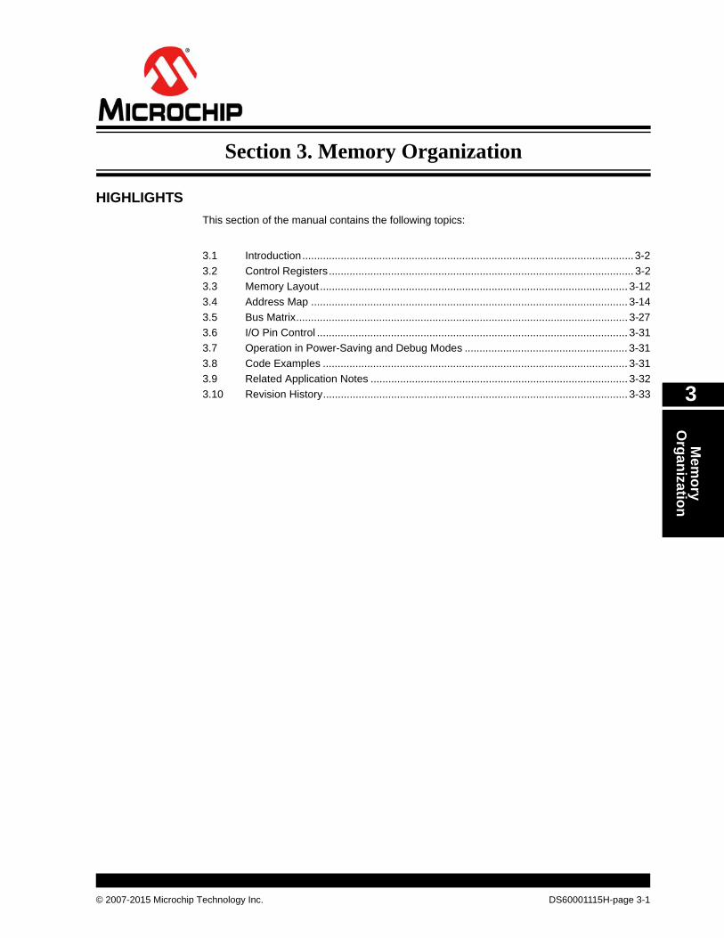
Register 3-4: BMXDUPBA: Data RAM User Program Base Address Register
Bit Range
Bit31/23/15/7
Bit30/22/14/6
Bit29/21/13/5
Bit28/20/12/4
Bit27/19/11/3
Bit26/18/10/2
Bit25/17/9/1
Bit24/16/8/0
31:24U-0 U-0 U-0 U-0 U-0 U-0 U-0 U-0
— — — — — — — —
23:16U-0 U-0 U-0 U-0 U-0 U-0 U-0 R/W-0
— — — — — — — BMXDUPBA<16>
15:8R/W-0 R/W-0 R/W-0 R/W-0 R/W-0 R/W-0 R-0 R-0
BMXDUPBA<15:8>
7:0R-0 R-0 R-0 R-0 R-0 R-0 R-0 R-0
BMXDUPBA<7:0>
Legend:
R = Readable bit W = Writable bit U = Unimplemented bit, read as ‘0’
-n = Value at POR ‘1’ = Bit is set ‘0’ = Bit is cleared x = Bit is unknown
bit 31-17 Unimplemented: Read as ‘0’
bit 16-10 BMXDUPBA<16:10>: DRM User Program Base Address bits
When non-zero, the value selects the relative base address for User mode program space in RAM. Ifnon-zero, BMXDUPBA must be greater than BMXDUDBA.
bit 9-0 BMXDUPBA<9:0>: Read-only bits
Value is always ‘0’, which forces 1 KB increments.
Note 1: At Reset, the value in this register is forced to zero, which causes all of the RAM to be allocated to Kernel mode data usage.
2: The value in this register must be less than or equal to BMXDRMSZ.
DS60001115H-page 3-8 © 2007-2015 Microchip Technology Inc.

Section 3. Memory OrganizationM
emo
ry
Org
anizatio
n
3
Register 3-5: BMXDRMSZ: Data RAM Size Register
Bit Range
Bit31/23/15/7
Bit30/22/14/6
Bit29/21/13/5
Bit28/20/12/4
Bit27/19/11/3
Bit26/18/10/2
Bit25/17/9/1
Bit24/16/8/0
31:24R R R R R R R R
BMXDRMSZ<31:24>
23:16R R R R R R R R
BMXDRMSZ<23:16>
15:8R R R R R R R R
BMXDRMSZ<15:8>
7:0R R R R R R R R
BMXDRMSZ<7:0>
Legend:
R = Readable bit W = Writable bit U = Unimplemented bit, read as ‘0’
-n = Value at POR ‘1’ = Bit is set ‘0’ = Bit is cleared x = Bit is unknown
bit 31-0 BMXDRMSZ<31:0>: Data RAM Memory (DRM) Size bits
Static value that indicates the size of the Data RAM in bytes:0x00002000 = device has 8 KB RAM0x00004000 = device has 16 KB RAM0x00008000 = device has 32 KB RAM0x00010000 = device has 64 KB RAM0x00020000 = device has 128 KB RAM
© 2007-2015 Microchip Technology Inc. DS60001115H-page 3-9

PIC32 Family Reference Manual
Register 3-6: BMXPUPBA: Program Flash Memory User Program Base Address Register
Bit Range
Bit31/23/15/7
Bit30/22/14/6
Bit29/21/13/5
Bit28/20/12/4
Bit27/19/11/3
Bit26/18/10/2
Bit25/17/9/1
Bit24/16/8/0
31:24U-0 U-0 U-0 U-0 U-0 U-0 U-0 U-0
— — — — — — — —
23:16U-0 U-0 U-0 U-0 R/W-0 R/W-0 R/W-0 R/W-0
— — — — BMXPUPBA<19:16>
15:8R/W-0 R/W-0 R/W-0 R/W-0 R/W-0 R-0 R-0 R-0
BMXPUPBA<15:8>
7:0R-0 R-0 R-0 R-0 R-0 R-0 R-0 R-0
BMXPUPBA<7:0>
Legend:
R = Readable bit W = Writable bit U = Unimplemented bit, read as ‘0’
-n = Value at POR ‘1’ = Bit is set ‘0’ = Bit is cleared x = Bit is unknown
bit 31-20 Unimplemented: Read as ‘0’
bit 19-11 BMXPUPBA<19:11>: Program Flash User Program Base Address bits
bit 10-0 BMXPUPBA<10:0>: Read-only bits
Value is always ‘0’, which forces 2 KB increments.
Note 1: At Reset, the value in this register is forced to zero, which causes all of the RAM to be allocated to Kernel mode program usage.
2: The value in this register must be less than or equal to BMXPFMSZ.
Register 3-7: BMXPFMSZ: Program Flash Memory Size Register
Bit Range
Bit31/23/15/7
Bit30/22/14/6
Bit29/21/13/5
Bit28/20/12/4
Bit27/19/11/3
Bit26/18/10/2
Bit25/17/9/1
Bit24/16/8/0
31:24R R R R R R R R
BMXPFMSZ<31:24>
23:16R R R R R R R R
BMXPFMSZ<23:16>
15:8R R R R R R R R
BMXPFMSZ<15:8>
7:0R R R R R R R R
BMXPFMSZ<7:0>
Legend:
R = Readable bit W = Writable bit U = Unimplemented bit, read as ‘0’
-n = Value at POR ‘1’ = Bit is set ‘0’ = Bit is cleared x = Bit is unknown
bit 31-0 BMXPFMSZ<31:0>: Program Flash Memory Size bits
Static value that indicates the size of the PFM in bytes:0x00008000 = device has 32 KB Flash0x00010000 = device has 64 KB Flash0x00020000 = device has 128 KB Flash0x00040000 = device has 256 KB Flash0x00080000 = device has 512 KB Flash
DS60001115H-page 3-10 © 2007-2015 Microchip Technology Inc.

Section 3. Memory OrganizationM
emo
ry
Org
anizatio
n
3
Register 3-8: BMXBOOTSZ: Boot Flash (IFM) Size Register
Bit Range
Bit31/23/15/7
Bit30/22/14/6
Bit29/21/13/5
Bit28/20/12/4
Bit27/19/11/3
Bit26/18/10/2
Bit25/17/9/1
Bit24/16/8/0
31:24R R R R R R R R
BMXBOOTSZ<31:24>
23:16R R R R R R R R
BMXBOOTSZ<23:16>
15:8R R R R R R R R
BMXBOOTSZ<15:8>
7:0R R R R R R R R
BMXBOOTSZ<7:0>
Legend:
R = Readable bit W = Writable bit U = Unimplemented bit, read as ‘0’
-n = Value at POR ‘1’ = Bit is set ‘0’ = Bit is cleared x = Bit is unknown
bit 31-0 BMXBOOTSZ<31:0>: Boot Flash Memory (BFM) Size bits
Static value that indicates the size of the Boot PFM in bytes. Refer to the “Memory Organization” chapterin the specific device data sheet for the available bit values.
© 2007-2015 Microchip Technology Inc. DS60001115H-page 3-11

PIC32 Family Reference Manual
3.3 MEMORY LAYOUT
The PIC32 microcontrollers implement two address spaces: virtual and physical. All hardwareresources, such as program memory, data memory and peripherals, are located at their respec-tive physical addresses. Virtual addresses are exclusively used by the CPU to fetch and executeinstructions. Physical addresses are used by peripherals, such as DMA and Flash controllers,that access memory independently of the CPU.
Figure 3-1: Virtual to Physical Fixed Memory Mapping Example
VirtualMemory Map
Physical Memory Map
0xFFFFFFFFReserved
Reserved
0xFFFFFFFF0xBFC030000xBFC02FFF Device
Configuration Registers0xBFC02FF0
0xBFC02FEFBoot Flash
0xBFC00000
Reserved0xBF9000000xBF8FFFFF
SFRs0xBF800000
Reserved0xBD0080000xBD007FFF
Program Flash(2)
0xBD000000
Reserved0xA00020000xA0001FFF
RAM(2)
0xA0000000 0x1FC03000
ReservedDevice
ConfigurationRegisters
0x1FC02FFF0x9FC030000x9FC02FFF Device
ConfigurationRegisters
0x1FC02FF0
Boot Flash0x1FC02FEF
0x9FC02FEF0x9FC02FEF
Boot Flash0x1FC00000
Reserved0x9FC00000 0x1F900000
Reserved SFRs0x1F8FFFFF
0x9D008000 0x1F8000000x9D007FFF
Program Flash(2) Reserved0x9D000000 0x1D008000
ReservedProgram Flash(2)
0x1D007FFF0x800020000x80001FFF
RAM(2)0x1D000000
Reserved0x80000000 0x00002000
Reserved RAM(2) 0x00001FFF0x00000000 0x00000000
Note 1: Memory areas are not shown to scale.
2: The size of this memory region is programmable and can be changed by initialization code provided by end-user developmenttools (refer to the specific development tool documentation for information).
KS
EG
1K
SE
G0
DS60001115H-page 3-12 © 2007-2015 Microchip Technology Inc.

Section 3. Memory OrganizationM
emo
ry
Org
anizatio
n
3
The entire 4 GB virtual address space is divided into two primary regions: user and kernel space.The lower 2 GB of space from the User mode segment is called USEG/KUSEG. A User modeapplication must reside and execute in the USEG segment. The USEG segment is also availableto all Kernel mode applications, which is why it is also named KUSEG – to indicate that it isavailable to both User and Kernel modes. When operating in User mode, the bus matrix must beconfigured to make part of the Flash and data memory available in the USEG/KUSEG segment.See 3.4 “Address Map” for more information.
Figure 3-2: User/Kernel Address Segments
The upper 2 GB of virtual address space forms the kernel only space. The kernel space is dividedinto four segments of 512 MB each: KSEG0, KSEG1, KSEG2 and KSEG3. Only Kernel modeapplications can access kernel space memory. The kernel space includes all peripheral registers.Consequently, only Kernel mode applications can monitor and manipulate peripherals. OnlyKSEG0 and KSEG1 segments point to real memory resources. Segment KSEG2 is available tothe EJTAG probe debugger, as explained in the MIPS documentation (refer to the EJTAGspecification). The PIC32 only uses KSEG0 and KSEG1 segments. The Boot Flash Memory(BFM), Program Flash Memory (PFM), Data RAM Memory (DRM) and peripheral SFRs areaccessible from either KSEG0 or KSEG1, while the peripheral SFRs are accessible only fromKSEG1.
The Fixed Mapping Translation (FMT) unit translates the memory segments into correspondingphysical address regions. Figure 3-1 illustrates the fixed mapping scheme implemented by thePIC32 core between the virtual and physical address space. A virtual memory segment may alsobe cached, provided the cache module is available on the device. The KSEG1 memory segmentis not cacheable, while KSEG0 and USEG/KUSEG are cacheable.
The mapping of the memory segments depend on the CPU error level (set by the ERL bit in theCPU Status register). Error Level is set (ERL = 1) by the CPU on a Reset, Soft Reset or NMI. Inthis mode, the processor runs in Kernel mode and USEG/KUSEG are treated as unmapped anduncached regions, and the mapping in Figure 3-1 does not apply. This mode is provided forcompatibility with other MIPS processor cores that use a TLB-based MMU. The C start-up codeclears the ERL bit to zero, so that when application software starts up, it sees the proper virtualto physical memory mapping as illustrated in Figure 3-1.
KSEG0 and KSEG1 segments are always translated to physical address 0x0. This translationarrangement allows the CPU to access identical physical addresses from two separate virtualaddresses: one from KSEG0 and the other from KSEG1. As a result, the application can chooseto execute the same piece of code as either cached or uncached. See Section 4. “PrefetchCache Module” (DS61119) for more details. The on-chip peripherals are visible through KSEG1segment only (uncached access).
KernelSegments
(KSEG0,1,2,3)
User/KernelSegment
(USEG/KUSEG)
0xFFFFFFFF
0x800000000x7FFFFFFF
0x00000000
© 2007-2015 Microchip Technology Inc. DS60001115H-page 3-13

PIC32 Family Reference Manual
3.4 ADDRESS MAP
The Program Flash Memory is divided into kernel and user partitions. The kernel program Flash space starts at physical address 0x1D000000, whereas the user program Flash space starts at physical address 0xBD000000 + BMXPUPBA register value. Similarly, the internal RAM is also divided into kernel and user partitions. The kernel RAM space starts at physical address 0x00000000, whereas the user RAM space starts at physical address 0xBF000000 + BMXDUDBA register value. By default, the full Flash memory and RAM are mapped to Kernel mode application only.
The BMXxxxBA register settings must match the memory model of the target software applica-tion. If the linked code does not match the register values, the program may not run and maygenerate bus error exceptions on start-up.
3.4.1 Virtual to Physical Address Calculation (and Vice-Versa)
To translate the kernel address (KSEG0 or KSEG1) to a physical address, perform a “BitwiseAND” operation of the virtual address with 0x1FFFFFFF:
• Physical Address = Virtual Address & 0x1FFFFFFF
For physical address to KSEG0 virtual address translation, perform a “Bitwise OR” operation ofthe physical address with 0x80000000:
• KSEG0 Virtual Address = Physical Address | 0x80000000
For physical address to KSEG1 virtual address translation, perform a “Bitwise OR” operation ofthe physical address with 0xA0000000:
• KSEG1 Virtual Address = Physical Address | 0xA0000000
To translate from KSEG0 to KSEG1 virtual address, perform a “Bitwise OR” operation of theKSEG0 virtual address with 0x20000000:
• KSEG1 Virtual Address = KSEG0 Virtual Address | 0x20000000
Note: The Program Flash Memory is not writable through its address map. A write to thePFM address range causes a bus error exception.
DS60001115H-page 3-14 © 2007-2015 Microchip Technology Inc.

Section 3. Memory OrganizationM
emo
ry
Org
anizatio
n
3
Table 3-2: Address Map
Memory TypeVirtual Addresses Physical Addresses Size in Bytes
Begin Address End Address Begin Address End Address Calculation
Ker
nel
Ad
dre
ss S
pac
e
Boot Flash 0xBFC00000 0xBFC02FFF 0x1FC00000 0x1FC02FFF 12 KB
Peripheral 0xBF800000 0xBF8FFFFF 0x1F800000 0x1F8FFFFF 4 KB
KSEG1 Program Flash(1,3)
0xBD000000 0xBD000000 +BMXPUPBA - 1
0x1D000000 0x1D00000 +BMXPUPBA - 1
BMXPUPBA
KSEG1 Program RAM(6)
0xA0000000 + BMXDKPBA
0xA0000000 + BMXDUDBA - 1
0x00000000 + BMXDKPBA
0x00000000 + BMXDUDBA - 1
BMXDUDBA - BMXDKPBA
KSEG1 Data RAM(6)
0xA0000000 0xA0000000 + BMXDKPBA - 1
0x00000000 0x00000000 + BMXDKPBA - 1
BMXPUPBA
KSEG0 Program Flash(2,5)
0x9D000000 0x9D000000 + BMXPUPBA - 1
0x1D000000 0x1D000000 + BMXPUPBA - 1
BMXPUPBA
KSEG0 Pro-gram RAM(6)
0x80000000 + BMXDKPBA
0x80000000 + BMXDUDBA - 1
0x00000000 + BMXDKPBA
0x00000000 + BMXDUDBA - 1
BMXDUDBA - BMXDKPBA
KSEG0 Data RAM(6)
0x80000000 0x80000000 + BMXDKPBA - 1
0x00000000 0x00000000 + BMXDKPBA - 1
BMXDKPBA
Memory TypeVirtual Addresses Physical Addresses Size in Bytes
Begin Address End Address Begin Address End Address Calculation
Us
er A
dd
ress
Sp
ace USEG/KSEG
Program RAM(6)
0x7F000000 + BMXDUPBA
0x7F000000 + BMXDRMSZ -1(3)
0xBF000000 + BMXDUPBA
0xBF000000 + BMXDRMSZ(3) - 1
BMXDRMSZ(3) -BMXDUPBA
USEG/KSEG Data RAM(6)
0x7F000000 + BMXDUDBA
0x7F000000 + BMXDUPBA - 1
0xBF000000 + BMXDUDBA
0xBF000000 + BMXDUPBA - 1
BMXDUPBA - BMXDUDBA
USEG/KSEG Program Flash(6)
0x7D000000 + BMXPUPBA
0x7D000000 + BMXPFMSZ(4) - 1
0xBD000000 + BMXPUPBA
0xBF000000 + BMXPFMSZ(4) - 1
BMXPFMSZ(4) - BMXPUPBA
Note 1: Program Flash virtual addresses in the non-cacheable range (KSEG1).
2: Program Flash virtual addresses in the cacheable and prefetchable range (KSEG0).
3: The RAM size varies between PIC32 device variants.
4: The Flash size varies between PIC32 device variants.
5: When the BMXPUPBA register is equal to ‘0’, all program Flash is allocated to Kernel mode program usage. This is the default state at Reset.
6: When the BMXDUDBA, BMXDUPBA, or BMXDKPBA register is equal to ‘0’, all RAM is allocated to Kernel mode data usage. This is the default state at Reset.
© 2007-2015 Microchip Technology Inc. DS60001115H-page 3-15

PIC32 Family Reference Manual
3.4.2 Program Flash Memory Partitioning
The Program Flash Memory can be partitioned for User and Kernel mode programs as illustratedin Figure 3-1.
At Reset, the User mode partition does not exist (BMXPUPBA is initialized to ‘0’). The entireprogram Flash memory is mapped to Kernel mode program space starting at virtual addressKSEG1:0xBD000000 (or KSEG0:0x9D000000). To set up a partition for the User mode program,initialize BMXPUPBA as follows:
• BMXPUPBA = BMXPFMSZ – USER_FLASH_PGM_SZ
The USER_FLASH_PGM_SZ is the partition size of the User mode program. BMXPFMSZ is thebus matrix register that holds the total size of program Flash memory.
Example:
• Assuming the PIC32 device has 512 Kbytes of Flash memory, the BMXPFMSZ will contain 0x00080000.
• To create a user Flash program partition of 20 Kbytes (0x5000): BMXPUPBA = 0x80000 – 0x5000 = 0x7B000
The size of the user Flash will be 20K and the size left for the kernel Flash will be 512 Kbytes – 20 Kbytes = 492 Kbytes.
The user Flash partition will extend from 0x7D07B000 to 0x7D07FFFF (virtual addresses).
The Kernel mode partition always starts from KSEG1:0xBD000000 or KSEG0:0x9D000000. Inthe above example, the kernel partition will extend from 0xBD000000 to 0xBD07AFFF(492 Kbytes in size).
Figure 3-3: Flash Partitioning
Note 1: Kernel Flash Size = BMXPUPBA.
2: User Flash Size = BMXPFMSZ-BMXPUPBA.
3: If BMXPUPBA is ‘0’, then:K Flash Size = BMXPFMSZ (i.e., all the Flash)User Flash Size = 0
Physical Address
0x1D000000
Virtual Address
KSEG0: 0x9D000000+BMXPUPBA
+BMXPUPBAKSEG1: 0xBD000000
KSEG0: 0x9D000000KSEG1: 0xBD000000
0x7D000000+BMXPUPBA
0x00000000
0xBD000000+
BMXPUPBA
Kernel F
lash Size
(1)
User F
lash Size
(2)
Flash Partition forKernel Program
(KSEG 0/1)
OptionalFlash Partition for
User Program(USEG/KUSEG)
DS60001115H-page 3-16 © 2007-2015 Microchip Technology Inc.

Section 3. Memory OrganizationM
emo
ry
Org
anizatio
n
3
3.4.3 RAM Partitioning
The RAM memory can be divided into four partitions:
• Kernel Data
• Kernel Program
• User Data
• User Program
To execute from data RAM, a kernel or user program partition must be defined. At Power-onReset (POR), the entire data RAM is assigned to the kernel data partition. This partition alwaysstarts from the base of the data RAM. See Figure 3-4 for more information.
Figure 3-4: RAM Partitioning
Note 1: To partition the RAM, you must program all of the following registers: BMXDKPBA,BMXDUDBA and BMXDUPBA.
2: The size of the available RAM is given by the BMXDRMSZ register.
Note 1: Kernel Data RAM Size = BMXDKPBA.
2: Kernel Program RAM Size = BMXDUDBA - BMXDKPBA.
3: User Data RAM Size = BMXDUPBA - BMXDUDBA.
4: User Program RAM Size = BMXDRMSZ - BMXDUPBA.
5: If BMXDKPBA, BMXDUDBA or BMXDUPBA is ‘0’, then:Kernel Data RAM Size = BMXDRMSZ (i.e., all RAM)Kernel Program RAM Size = 0User Data RAM Size = 0User Program RAM Size = 0
Physical Address
0x00000000
Virtual Address
KSEG0: 0x80000000+BMXDUDBA
+BMXDUDBAKSEG1: 0xA0000000
KSEG0: 0x80000000
KSEG1: 0xA0000000
0x7F000000+BMXDUPBA
0x00000000
0xBF000000 +BMXDUPBA
Kernel P
rogramU
ser Program
OptionalKernel Program Partition
KSEG 0/1
Kernel Data PartitionKSEG 0/1
+BMXDKPBA
+BMXDKPBA
KSEG0: 0x80000000KSEG1: 0xA0000000
0x7F000000+BMXDUDBA
+BMXDUDBA
0x00000000
0x00000000
0xBF000000
+BMXDKPBA
+BMXDUDBA
Kernel D
ataU
ser Da
ta
OptionalUser Program RAM Partition
(USEG/KUSEG)
OptionalUser RAM Partition
(USEG/KUSEG)
RA
M S
ize(2)
RA
M S
ize(1
) R
AM
Size
(4) R
AM
Size
(3)
© 2007-2015 Microchip Technology Inc. DS60001115H-page 3-17

PIC32 Family Reference Manual
3.4.3.1 Kernel Data RAM Partition
The kernel data RAM partition is located at virtual address KSEG0:0x80000000,KSEG1:0xA0000000. It is always active and cannot be disabled.
If any of the BMXDKPBA, BMXDUDBA or BMXDUPBA registers is ‘0’, the entire RAM isassigned to kernel data RAM (i.e., the size of the kernel data RAM partition is given by the BMX-DRMSZ register value; see Figure 3-5). Otherwise, the size of the kernel data RAM partition isgiven by the value of the BMXDKPBA register (see Figure 3-6).
The kernel data RAM partition exists on Reset and takes up all the available RAM, as theBMXDKPBA, BMXDUDBA and BMXDUPBA registers default to zero at any Reset.
Figure 3-5: RAM Partitioning When BMXDKPBA, BMXDUDBA or BMXDUPBA = 0
Note: Kernel Data RAM Size = BMXDRMSZ.
Physical AddressVirtual Address
Kernel Data RAM PartitionKSEG0/1
KSEG0: 0x80000000KSEG1: 0xA0000000
BMXDRMSZ
Kerne
l Data R
AM
Size
DS60001115H-page 3-18 © 2007-2015 Microchip Technology Inc.

Section 3. Memory OrganizationM
emo
ry
Org
anizatio
n
3
Figure 3-6: Kernel Data RAM Partitioning
Note 1: Kernel Data RAM Size = BMXDKPBA.
2: None of the registers BMXDKPBA, BMXDUDBA or BMXDUPBA = 0.
Physical AddressVirtual Address
BMXDRMSZ
Other Data RAM Partitions
Kernel Data RAM PartitionKSEG0/KSEG1
Kernel D
ata RA
M S
ize(1)
KSEG0: 0x80000000
KSEG1: 0xA0000000
+BMXDKPBA
+BMXDKPBA
KSEG0: 0x80000000KSEG1: 0xA0000000
© 2007-2015 Microchip Technology Inc. DS60001115H-page 3-19

PIC32 Family Reference Manual
3.4.3.2 Kernel Program RAM Partition
The kernel program RAM partition is required if code needs to be executed from data RAM inKernel mode.
This partition starts at KSEG0:0x80000000 + BMXDKPBA (KSEG1:0xA0000000 +BMXDKPBA), and its size is given by BMXDUDBA - BMXDKPBA (see Figure 3-7).
The kernel program RAM partition does not exist on Reset, as the BMXDKPBA and BMXDUDBAregisters default to zero at Reset.
Figure 3-7: Kernel Program RAM Partitioning
Note 1: Kernel Program RAM Size = BMXDUDBA - BMXDKPBA.
2: None of BMXDKPBA, BMXDUDBA or BMXDUPBA = 0.
Physical AddressVirtual Address
BMXDRMSZ
User Data RAM Partitions
Kernel Program RAM PartitionKSEG 0/1
Kernel Data RAM PartitionKSEG0/KSEG1
Kernel P
rogram R
AM
Size
(1)K
ernel D
ata RA
M S
ize
KSEG0: 0x80000000
KSEG1: 0xA0000000
+BMXDKPBA
+BMXDKPBA
KSEG0: 0x80000000
KSEG1: 0xA0000000
+BMXDUDBA
+BMXDUDBA
KSEG1: 0xA0000000KSEG0: 0x80000000
DS60001115H-page 3-20 © 2007-2015 Microchip Technology Inc.

Section 3. Memory OrganizationM
emo
ry
Org
anizatio
n
3
3.4.3.3 User Data RAM Partition
For User mode applications, a User mode data partition in RAM is required. This partition startsat address 0x7F000000 + BMXDUDBA, and its size is given by BMXDUPBA - BMXDUDBA (seeFigure 3-8).
The user data RAM partition does not exist on Reset, as the BMXDUDBA and BMXDUPBAregisters default to zero at Reset.
Figure 3-8: User Data RAM Partitioning
Note 1: User Data RAM Size = BMXDUPBA - BMXDUDBA.
2: None of the registers BMXDKPBA, BMXDUDBA or BMXDUPBA = 0.
Physical AddressVirtual Address
BMXDRMSZ
User Program RAM Partitions
User Data RAM Partitions
User D
ata RA
M S
ize(1)
0x7F000000+BMXDUDBA
0x7F000000+BMXDUPBA
© 2007-2015 Microchip Technology Inc. DS60001115H-page 3-21

PIC32 Family Reference Manual
3.4.3.4 User Program RAM Partition
The user program partition in data RAM is required if code needs to be executed from data RAMin User mode. This partition starts at address 0x7F000000 + BMXDUPBA, and its size is givenby BMXDRMSZ – BMXDUPBA (see Figure 3-9).
The User Program RAM partition does not exist on Reset, as the BMXDUPBA register defaultsto zero at Reset.
Figure 3-9: User Program RAM Partitioning
Note 1: User Program RAM Size = BMXDRMSZ - BMXDUPBA.
2: None of the registers BMXDKPBA, BMXDUDBA or BMXDUPBA = 0.
Physical AddressVirtual Address
BMXDRMSZ
User Program RAM Partition
User Data RAM Partition
User P
rogram R
AM
Size
(1)
0x7F000000+BMXDUDBA
0x7F000000+BMXDUPBA
DS60001115H-page 3-22 © 2007-2015 Microchip Technology Inc.

Section 3. Memory OrganizationM
emo
ry
Org
anizatio
n
3
3.4.3.5 RAM Partitioning Examples
This section provides the following practical examples of RAM partitioning:
• RAM Partitioned as Kernel Data
• RAM Partitioned as Kernel Data and Kernel Program
• RAM Partitioned as Kernel Data and User Data
• RAM Partitioned as Kernel Data, Kernel Program and User Data
• RAM Partitioned as Kernel Data, Kernel Program, User Data and User Program
3.4.3.5.1 Example 1. RAM Partitioned as Kernel Data
The entire RAM is partitioned as kernel data RAM after a Reset. No other programming isrequired. Setting the BMXDKPBA, BMXDUDBA or BMXDUPBA register to ‘0’ will partition theentire RAM space to a kernel data partition (see Figure 3-5).
3.4.3.5.2 Example 2. RAM Partitioned as Kernel Data and Kernel Program
For this example, assume that the available RAM on the PIC32 device is 32 KB, of which 8 KBkernel data RAM and 24 KB of kernel program RAM are needed. In this example, the user dataRAM and user program RAM will have their sizes set to ‘0’.
A kernel data RAM partition is always required (see Figure 3-10 for more information).
The values of the registers are as follows:
• BMXDRMSZ = 0x00008000 (read-only value)
• BMXDKPBA = 0x00002000 (i.e., 8 KB kernel data)
• BMXDUDBA = 0x00008000 (i.e., 0x6000 kernel program)
• BMXDUPBA = 0x00008000 (i.e., user data size = 0, and user program size = 0)
Figure 3-10: RAM Partitioning for 8 KB Kernel Data and 16 KB Kernel Program
BMXDKPBA = 0x2000BMXDUDBA = 0x8000BMXDUPBA = 0x8000
Note: Only KSEG0 addresses are shown. For KSEG1 addresses, start at 0xA000000.
Physical AddressVirtual Address
BMXDRMSZ
Kernel Data RAM Partition
Kernel Program RAM Partition
Kernel P
rogram
RA
M S
ize
= 0x80000000
+BMXDKPBA
KSEG0: 0x80008000
+BMXDUDBA
Kernel D
ata RA
M S
ize
= 0x00008000
KSEG 0/124 KB
KSEG 0/18 KB
= 0x80000000KSEG0: 0x80002000
KSEG0: 0x80000000
© 2007-2015 Microchip Technology Inc. DS60001115H-page 3-23
PIC32 Family Reference Manual
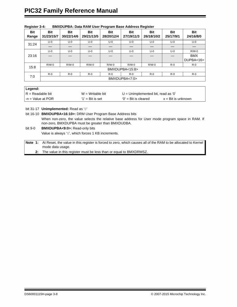
3.4.3.5.3 Example 3. RAM Partitioned as Kernel Data and User Data
For this example, assume that the available RAM on the PIC32 device is 32 KB, of which 16 KBof kernel data RAM and 16 KB of user data RAM are needed. In this example, the kernel programRAM and user program RAM will have their sizes set to ‘0’. See Figure 3-11 for details.
The values of the registers are as follows:
• BMXDRMSZ = 0x00008000 (read-only value)
• BMXDKPBA = 0x00004000 (i.e., 16 KB kernel data)
• BMXDUDBA = 0x00004000 (i.e., 0 kernel program)
• BMXDUPBA = 0x00008000 (i.e., user data size = 16 KB, and user program size = 0)
Figure 3-11: RAM Partitioning for 16 KB Kernel Data and 16 KB User Data
BMXDKPBA = 0x4000BMXDUDBA = 0x4000BMXDUPBA = 0x8000
Note: Only KSEG0 addresses are shown. For KSEG1 addresses, start at 0xA0000000.
Physical AddressVirtual Address
KSEG0: 0x80004000= 0x80000000+BMXDKPBA
KSEG0: 0x80000000
0x7F008000= 0x7F000000+BMXDUPBA
0x00000000
Kernel D
ata R
AM
Size
User D
ata RA
M S
ize
User Data RAM16 KB
Kernel Data RAM16 KB
0x7F004000= 0x7F000000+BMXDUDBA
DS60001115H-page 3-24 © 2007-2015 Microchip Technology Inc.

Section 3. Memory OrganizationM
emo
ry
Org
anizatio
n
3
3.4.3.5.4 Example 4. RAM Partitioned as Kernel Data, Kernel Program and User Data
For this example, assume that the available RAM on the PIC32 device is 32 KB, and 4 KB ofkernel data RAM, 6 KB of kernel program and 22 KB of user data RAM are needed. In thisexample, the user program RAM will have its size set to ‘0’. See Figure 3-12 for details.
The values of the registers are as follows:
• BMXDRMSZ = 0x00008000 (read-only value)
• BMXDKPBA = 0x00001000 (i.e., 4 KB kernel data)
• BMXDUDBA = 0x00002800 (i.e., 6 KB kernel program)
• BMXDUPBA = 0x00008000 (i.e., user data size = 22 KB, and user program size = 0)
Figure 3-12: RAM Partitioning for 4 KB K-Data, 6 KB K-Program and 22 KB U-Data
BMXDKPBA = 0x1000BMXDUDBA = 0x2800BMXDUPBA = 0x8000
Note: Only KSEG0 addresses are shown. For KSEG1 addresses, start at 0xA0000000.
Physical AddressVirtual Address
KSEG0: 0x80002800= 0x80000000+BMXDUDBA
KSEG0: 0x80000000
0x7F008000= 0x7F000000+BMXDUPBA
0x00000000
Kern
el Da
taU
ser Data R
AM
Size
User Data RAM22 KB
Kernel Program RAM6 KB
0x7F002800= 0x7F000000+BMXDUDBA
Kernel Data RAM4 KB
Kernel P
rogram
RA
M S
ize R
AM
Size
KSEG0: 0x80001000= 0x80000000+BMXDKPBA
© 2007-2015 Microchip Technology Inc. DS60001115H-page 3-25

PIC32 Family Reference Manual
3.4.3.5.5 Example 5. RAM Partitioned as Kernel Data, Kernel Program, User Data and User Program
For this example, assume that the available RAM on the PIC32 device is 32 KB, and 6 KB of ker-nel data RAM, 5 KB of kernel program RAM, 12 KB of user data RAM and 9 KB of user programRAM are needed. See Figure 3-13 for details.
The values of the registers are as follows:
• BMXDRMSZ = 0x00008000 (read-only value)
• BMXDKPBA = 0x00001800 (i.e., 6 KB kernel data)
• BMXDUDBA = 0x00002C00 (i.e., 5 KB kernel program)
• BMXDUPBA = 0x00005C00 (i.e., user data size = 12 KB, and user program size = 9 KB)
Figure 3-13: RAM Partitioning for 6 KB K-Data, 5 KB K-Program, 12 KB U-Data and 9 KB U-Program
BMXDKPBA = 0x1800BMXDUDBA = 0x2c00BMXDUPBA = 0x5c00
Note: Only KSEG0 addresses are shown. For KSEG1 addresses, start at 0xA0000000.
Physical AddressVirtual Address
KSEG0: 0x80002C00= 0x80000000+BMXDUDBA
KSEG0: 0x80000000
0x7F005C00= 0x7F000000+BMXDUPBA
0x00000000
Kernel D
ataU
ser D
ata
User Program RAM9 KB
Kernel Program RAM5 KB
0x7F002C00= 0x7F000000+BMXDUDBA
Kernel Data RAM6 KB
Kernel P
rogram R
AM
Size
RA
M S
ize
KSEG0: 0x80001800= 0x80000000+BMXDKPBA
User Data RAM12 KB
RA
M S
izeU
ser Program
RA
M S
ize
0x7F008000= 0x7F000000+BMXDRMSZ
DS60001115H-page 3-26 © 2007-2015 Microchip Technology Inc.
Section 3. Memory OrganizationM
emo
ry
Org
anizatio
n
3
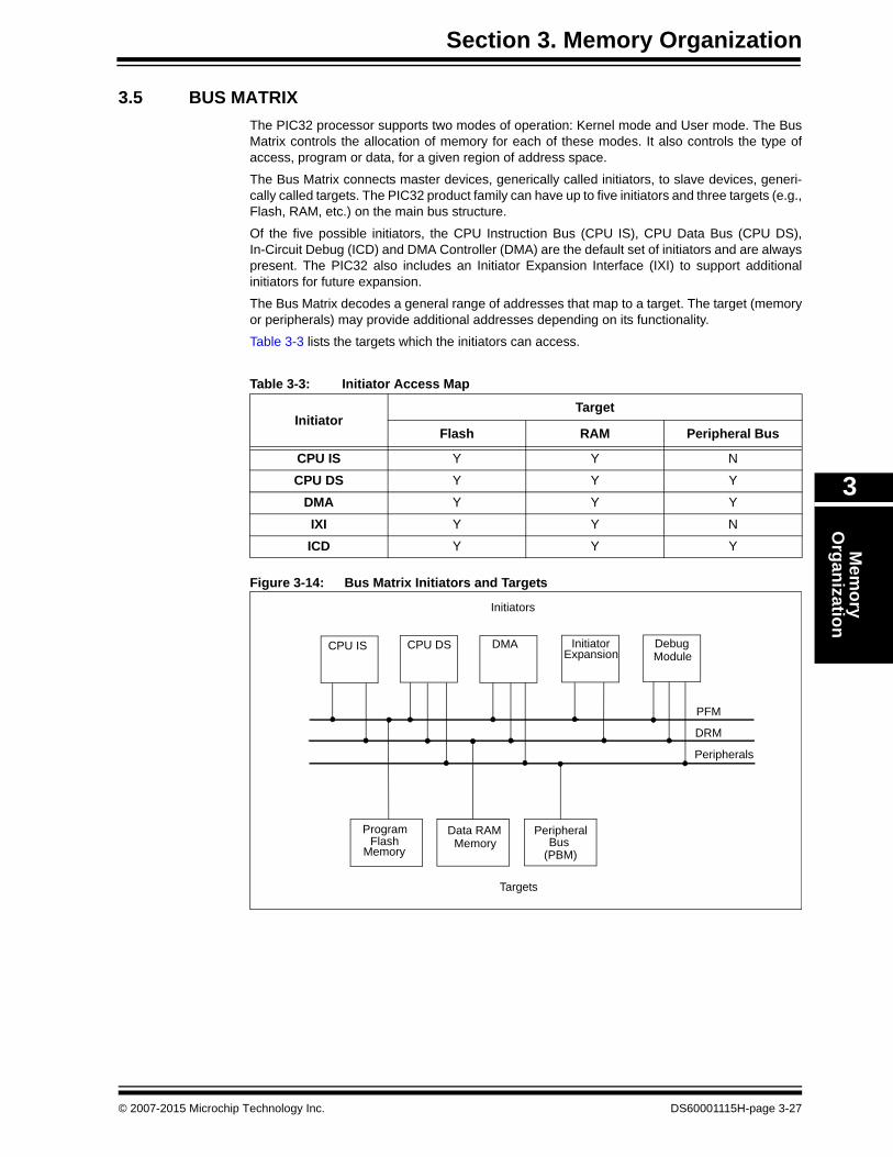
3.5 BUS MATRIX
The PIC32 processor supports two modes of operation: Kernel mode and User mode. The BusMatrix controls the allocation of memory for each of these modes. It also controls the type ofaccess, program or data, for a given region of address space.
The Bus Matrix connects master devices, generically called initiators, to slave devices, generi-cally called targets. The PIC32 product family can have up to five initiators and three targets (e.g.,Flash, RAM, etc.) on the main bus structure.
Of the five possible initiators, the CPU Instruction Bus (CPU IS), CPU Data Bus (CPU DS),In-Circuit Debug (ICD) and DMA Controller (DMA) are the default set of initiators and are alwayspresent. The PIC32 also includes an Initiator Expansion Interface (IXI) to support additionalinitiators for future expansion.
The Bus Matrix decodes a general range of addresses that map to a target. The target (memoryor peripherals) may provide additional addresses depending on its functionality.
Table 3-3 lists the targets which the initiators can access.
Table 3-3: Initiator Access Map
Figure 3-14: Bus Matrix Initiators and Targets
InitiatorTarget
Flash RAM Peripheral Bus
CPU IS Y Y N
CPU DS Y Y Y
DMA Y Y Y
IXI Y Y N
ICD Y Y Y
CPU IS CPU DS DMA InitiatorExpansion
DebugModule
PFM
DRM
Peripherals
Initiators
Targets
Program
Memory
Data RAMMemory
Peripheral
(PBM)Flash Bus
© 2007-2015 Microchip Technology Inc. DS60001115H-page 3-27

PIC32 Family Reference Manual
3.5.1 Initiator Arbitration Modes
Since there can be more than one initiator attempting to access the same target, an arbitrationscheme must be used to control access to the target. The arbitration modes assign priority levelsto all the initiators. The initiator with the higher priority level will always win target access over alower priority initiator.
3.5.1.1 Arbitration Mode 0
The fixed priority scheme in Arbitration Mode 0 is illustrated in Figure 3-15. The CPU data andinstruction access are given higher priority than DMA access. Since this mode can starve theDMA, choose this mode when DMA is not being used.
As illustrated in Figure 3-15, each initiator is assigned a fixed priority level. Programming the registerfield BMXARB (BMXCON<2:0>) to ‘0’ selects Mode 0 operation.
Figure 3-15: Priority Assignment in Arbitration Mode 0
ICD/Debug
CPU Data
CPUInstruction
Access
DMA
InitiatorExpansion
Hig
her
Prio
rity
Access
DS60001115H-page 3-28 © 2007-2015 Microchip Technology Inc.
Section 3. Memory OrganizationM
emo
ry
Org
anizatio
n
3
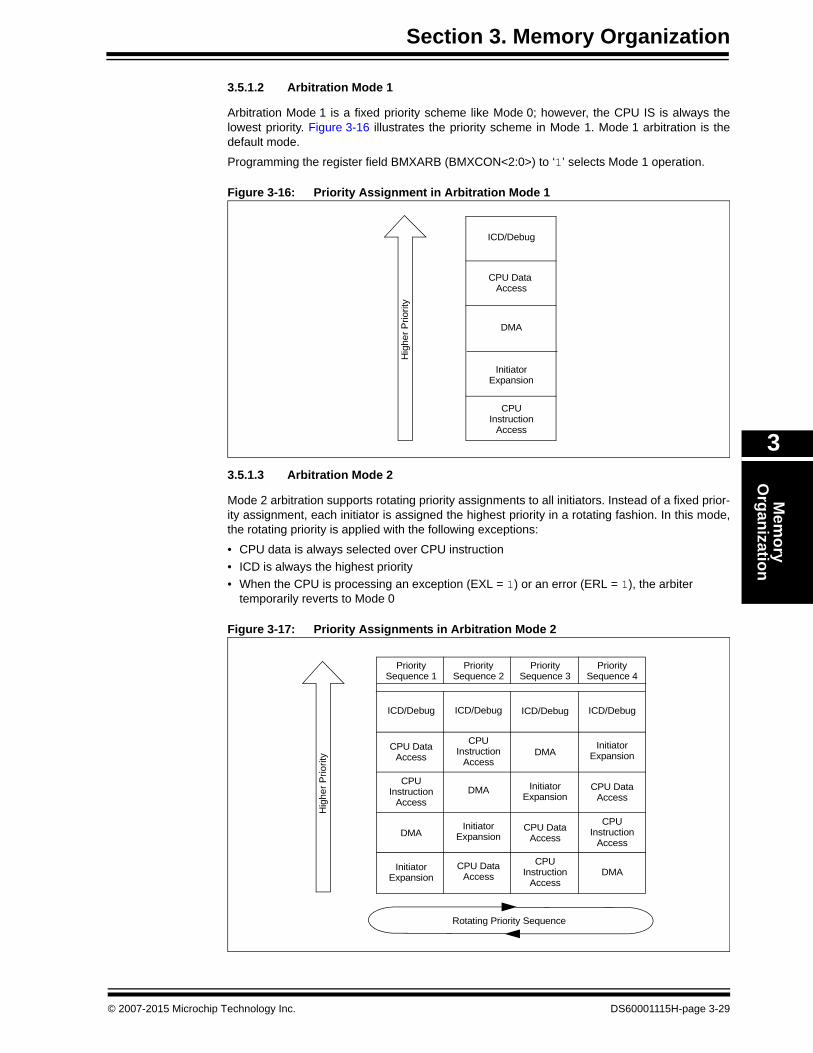
3.5.1.2 Arbitration Mode 1
Arbitration Mode 1 is a fixed priority scheme like Mode 0; however, the CPU IS is always thelowest priority. Figure 3-16 illustrates the priority scheme in Mode 1. Mode 1 arbitration is thedefault mode.
Programming the register field BMXARB (BMXCON<2:0>) to ‘1’ selects Mode 1 operation.
Figure 3-16: Priority Assignment in Arbitration Mode 1
3.5.1.3 Arbitration Mode 2
Mode 2 arbitration supports rotating priority assignments to all initiators. Instead of a fixed prior-ity assignment, each initiator is assigned the highest priority in a rotating fashion. In this mode,the rotating priority is applied with the following exceptions:
• CPU data is always selected over CPU instruction
• ICD is always the highest priority
• When the CPU is processing an exception (EXL = 1) or an error (ERL = 1), the arbiter temporarily reverts to Mode 0
Figure 3-17: Priority Assignments in Arbitration Mode 2
ICD/Debug
CPU Data
DMA
Initiator
CPUInstruction
Hig
her
Prio
rity
Access
Expansion
Access
PrioritySequence 1
PrioritySequence 2
PrioritySequence 3
PrioritySequence 4
ICD/Debug
CPU DataAccess
CPUInstruction
Access
DMA
InitiatorExpansion
ICD/Debug ICD/Debug ICD/Debug
CPUInstruction
Access
CPUInstruction
Access
CPUInstruction
Access
CPU DataAccess
CPU DataAccess
DMA
DMA
DMA
InitiatorExpansion
InitiatorExpansion
InitiatorExpansion
CPU DataAccess
Rotating Priority Sequence
Hig
he
r P
riorit
y
© 2007-2015 Microchip Technology Inc. DS60001115H-page 3-29
PIC32 Family Reference Manual
Note that priority sequence 2 is not selected in the rotating priority scheme if there is a pendingCPU data access. In this case, once the data access is complete, sequence 2 is selected.
Each target's arbiter state machine keeps track of which initiator last controlled it and re-ordersits priority separately from the other target arbiters. So if a target's priority sequence rotates witha data access pending, sequence 2 is skipped until the data access completes. This prevents aninstruction access from taking priority over a data access for that target.
Programming the BMXARB bit (BMXCON<2:0>) to ‘010’ selects Mode 2 operation.
3.5.2 Bus Error Exceptions
The Bus Matrix generates a bus error exception on:
• Any attempt to access unimplemented memory
• Any attempt to access an illegal target
• Any attempt to write to program Flash memory
Bus Error Exceptions may be temporarily disabled by clearing the BMXERRxxx bits in theBMXCON register, which is not recommended.
The Bus Matrix disables bus error exceptions for accesses from CPU IS and CPU DS while inDebug mode.
3.5.3 Break Exact Breakpoint Support
The PIC32 supports break exact breakpoints by inserting one Wait state to data RAM access.This method allows the CPU to stop execution before the breakpoint address instruction. This isuseful for breakpointed store instructions. When the Wait state is not used, the break will stilloccur at the store instruction, however, the DRM location is updated with the store value. If theWait state is enabled the DRM is not updated with the store value.
DS60001115H-page 3-30 © 2007-2015 Microchip Technology Inc.

Section 3. Memory OrganizationM
emo
ry
Org
anizatio
n
3
3.6 I/O PIN CONTROL
There are no I/O pins associated with this module.
3.7 OPERATION IN POWER-SAVING AND DEBUG MODES
3.7.1 Memory Operation on Power-up or Brown-out Reset (BOR):
• The contents of data RAM are undefined
• The BMX Base Address (BMXxxxBA) registers are reset to ‘0’
• The CPU is switched to Kernel mode
3.7.2 Memory Operation on Reset:
• The data RAM contents are retained. If the device is code-protected, the RAM contents are cleared
• The BMX base address registers (BMXxxxBA) are set to ‘0’
• The CPU is switched to Kernel mode
3.7.3 Memory Operation on Wake-up from Device Sleep or Idle Mode:
• The contents of data RAM are retained
• The contents of the BMX Base Address (BMXxxxBA) registers are not changed
• The CPU mode is unchanged
3.8 CODE EXAMPLES
Example 3-1: Create a User Mode Partition of 12K in Program Flash
Example 3-2: Create a Kernel Mode Data RAM Partition of 16K; Rest of RAM for Kernel Program
Example 3-3 can be used to create the following partitions in RAM:
• Kernel mode data = 12K
• Kernel mode program = 6K
• User mode data = 8K
• User mode program = 6K
Example 3-3: Create RAM Partitions
BMXPUPBA = BMXPFMSZ - (12*1024); // User Mode Flash 12K,// Kernel Mode Flash 500K (512K-12K)
BMXDKPBA = 16*1024;BMXDUDBA = BMXDRMSZ;BMXDUPBA = BMXDRMSZ;
BMXDKPBA = 12*1024; // Kernel Data Partition of 12K.// Start offset of Kernel Program Partition
BMXDUDBA = BMXDKPBA + (6*1024); // Kernel Program Partition of 6K// Start offset of User Data Partition
BMXDUPBA = BMXDUDBA + (8*1024); // User Data Partition of 8K// Start offset of User Program Partition.// This partition will go up to the size of// RAM (32K). So the partition size will be// 6K (32K - 8K - 6K - 12K)
© 2007-2015 Microchip Technology Inc. DS60001115H-page 3-31

PIC32 Family Reference Manual
3.9 RELATED APPLICATION NOTES
This section lists application notes that are related to this section of the manual. Theseapplication notes may not be written specifically for the PIC32 device family, but the concepts arepertinent and could be used with modification and possible limitations. The current applicationnotes related to the Memory Organization of the PIC32 family include the following:
Title Application Note #
No related application notes at this time. N/A
Note: Please visit the Microchip web site (www.microchip.com) for additional applicationnotes and code examples for the PIC32 family of devices.
DS60001115H-page 3-32 © 2007-2015 Microchip Technology Inc.

Section 3. Memory OrganizationM
emo
ry
Org
anizatio
n
3
3.10 REVISION HISTORY
Revision A (August 2007)
This is the initial released version of this document.
Revision B (October 2007)
Updated document to remove Confidential status.
Revision C (April 2008)
Revised status to Preliminary.
Revision D (June 2008)
Minor formatting updates to register tables.
Revision E (July 2009)
This revision includes the following updates:
• Minor updates to the text and formatting have been incorporated throughout the document
• Added Notes 1, 2 and 3, which describe the Clear, Set and Invert registers to the following:
- Table 3-1: Memory Organization SFR Summary
- Register 3-1: BMXCON: Bus Matrix Configuration
- Register 3-2: BMXDKPBA: Data RAM Kernel Program Base Address
- Register 3-3: BMXDUDBA: Data RAM User Data Base Address
- Register 3-4: BMXDUPBA: Data RAM User Program Base Address
- Register 3-6: BMXPUPBA: Program Flash Memory User Program Base Address
• Removed all Clear, Set, and Invert register descriptions
• Added additional bit value definition (0x0001000) to BMXDRMSZ: Data RAM Size Register (see Register 3-5)
Revision F (July 2010)
This revision includes the following updates:
• Minor updates to the text and formatting have been incorporated throughout the document
• Added Notes 4 and 5 to the following registers:
- BMXDKPBA: Data RAM Kernel Program Base Address Register (see Register 3-2)
- BMXDUDBA: Data RAM User Data Base Address Register (see Register 3-3)
- BMXDUPBA: Data RAM User Program Base Address Register (see Register 3-4)
- BMXPUPBA: Program Flash (PFM) User Program Base Address Register (see Register 3-6)
• Updated the PIC32 Address Map (see Table 3-2)
Revision G (July 2012)
This revision includes the following updates:
• All references to PIC32MX were changed to: PIC32
• Updated the notes in the Memory Organization SFR Summary (see Table 3-1)
• Removed the Clear, Set, and Invert register notes in all applicable register tables
• Updated the Virtual to Physical Fixed Memory Mapping Example (see Figure 3-1)
• Updated the Boot Flash Memory (BFM) Size bits value definition (see Register 3-8)
• Removed 3.9 “Design Tips”
• Minor updates to the text, as well as formatting changes have been incorporated throughout the document
© 2007-2015 Microchip Technology Inc. DS60001115H-page 3-33

PIC32 Family Reference Manual
Revision H (MAY 2015)
This revision includes the following updates:
• The following registers were updated:
- BMXDKPBA: Data RAM Kernel Program Base Address Register (see Register 3-2)
- BMXDUDBA: Data RAM User Data Base Address Register (see Register 3-3)
- BMXDUPBA: Data RAM User Program Base Address Register (see Register 3-4)
• 3.5.1.3 “Arbitration Mode 2” was updated
DS60001115H-page 3-34 © 2007-2015 Microchip Technology Inc.

Note the following details of the code protection feature on Microchip devices:
• Microchip products meet the specification contained in their particular Microchip Data Sheet.
• Microchip believes that its family of products is one of the most secure families of its kind on the market today, when used in the intended manner and under normal conditions.
• There are dishonest and possibly illegal methods used to breach the code protection feature. All of these methods, to our knowledge, require using the Microchip products in a manner outside the operating specifications contained in Microchip’s Data Sheets. Most likely, the person doing so is engaged in theft of intellectual property.
• Microchip is willing to work with the customer who is concerned about the integrity of their code.
• Neither Microchip nor any other semiconductor manufacturer can guarantee the security of their code. Code protection does not mean that we are guaranteeing the product as “unbreakable.”
Code protection is constantly evolving. We at Microchip are committed to continuously improving the code protection features of ourproducts. Attempts to break Microchip’s code protection feature may be a violation of the Digital Millennium Copyright Act. If such actsallow unauthorized access to your software or other copyrighted work, you may have a right to sue for relief under that Act.
Information contained in this publication regarding deviceapplications and the like is provided only for your convenienceand may be superseded by updates. It is your responsibility toensure that your application meets with your specifications.MICROCHIP MAKES NO REPRESENTATIONS ORWARRANTIES OF ANY KIND WHETHER EXPRESS ORIMPLIED, WRITTEN OR ORAL, STATUTORY OROTHERWISE, RELATED TO THE INFORMATION,INCLUDING BUT NOT LIMITED TO ITS CONDITION,QUALITY, PERFORMANCE, MERCHANTABILITY ORFITNESS FOR PURPOSE. Microchip disclaims all liabilityarising from this information and its use. Use of Microchipdevices in life support and/or safety applications is entirely atthe buyer’s risk, and the buyer agrees to defend, indemnify andhold harmless Microchip from any and all damages, claims,suits, or expenses resulting from such use. No licenses areconveyed, implicitly or otherwise, under any Microchipintellectual property rights.
2007-2015 Microchip Technology Inc.
QUALITY MANAGEMENT SYSTEM CERTIFIED BY DNV
== ISO/TS 16949 ==
Trademarks
The Microchip name and logo, the Microchip logo, dsPIC, FlashFlex, flexPWR, JukeBlox, KEELOQ, KEELOQ logo, Kleer, LANCheck, MediaLB, MOST, MOST logo, MPLAB, OptoLyzer, PIC, PICSTART, PIC32 logo, RightTouch, SpyNIC, SST, SST Logo, SuperFlash and UNI/O are registered trademarks of Microchip Technology Incorporated in the U.S.A. and other countries.
The Embedded Control Solutions Company and mTouch are registered trademarks of Microchip Technology Incorporated in the U.S.A.
Analog-for-the-Digital Age, BodyCom, chipKIT, chipKIT logo, CodeGuard, dsPICDEM, dsPICDEM.net, ECAN, In-Circuit Serial Programming, ICSP, Inter-Chip Connectivity, KleerNet, KleerNet logo, MiWi, MPASM, MPF, MPLAB Certified logo, MPLIB, MPLINK, MultiTRAK, NetDetach, Omniscient Code Generation, PICDEM, PICDEM.net, PICkit, PICtail, RightTouch logo, REAL ICE, SQI, Serial Quad I/O, Total Endurance, TSHARC, USBCheck, VariSense, ViewSpan, WiperLock, Wireless DNA, and ZENA are trademarks of Microchip Technology Incorporated in the U.S.A. and other countries.
SQTP is a service mark of Microchip Technology Incorporated in the U.S.A.
Silicon Storage Technology is a registered trademark of Microchip Technology Inc. in other countries.
GestIC is a registered trademarks of Microchip Technology Germany II GmbH & Co. KG, a subsidiary of Microchip Technology Inc., in other countries.
All other trademarks mentioned herein are property of their respective companies.
© 2007-2015, Microchip Technology Incorporated, Printed in the U.S.A., All Rights Reserved.
ISBN: 978-1-63277-374-6
DS60001115H-page 3-35
Microchip received ISO/TS-16949:2009 certification for its worldwide headquarters, design and wafer fabrication facilities in Chandler and Tempe, Arizona; Gresham, Oregon and design centers in California and India. The Company’s quality system processes and procedures are for its PIC® MCUs and dsPIC® DSCs, KEELOQ® code hopping devices, Serial EEPROMs, microperipherals, nonvolatile memory and analog products. In addition, Microchip’s quality system for the design and manufacture of development systems is ISO 9001:2000 certified.

DS60001115H-page 3-36 2007-2015 Microchip Technology Inc.
AMERICASCorporate Office2355 West Chandler Blvd.Chandler, AZ 85224-6199Tel: 480-792-7200 Fax: 480-792-7277Technical Support: http://www.microchip.com/supportWeb Address: www.microchip.com
AtlantaDuluth, GA Tel: 678-957-9614 Fax: 678-957-1455
Austin, TXTel: 512-257-3370
BostonWestborough, MA Tel: 774-760-0087 Fax: 774-760-0088
ChicagoItasca, IL Tel: 630-285-0071 Fax: 630-285-0075
ClevelandIndependence, OH Tel: 216-447-0464 Fax: 216-447-0643
DallasAddison, TX Tel: 972-818-7423 Fax: 972-818-2924
DetroitNovi, MI Tel: 248-848-4000
Houston, TX Tel: 281-894-5983
IndianapolisNoblesville, IN Tel: 317-773-8323Fax: 317-773-5453
Los AngelesMission Viejo, CA Tel: 949-462-9523 Fax: 949-462-9608
New York, NY Tel: 631-435-6000
San Jose, CA Tel: 408-735-9110
Canada - TorontoTel: 905-673-0699 Fax: 905-673-6509
ASIA/PACIFICAsia Pacific OfficeSuites 3707-14, 37th FloorTower 6, The GatewayHarbour City, KowloonHong KongTel: 852-2943-5100Fax: 852-2401-3431
Australia - SydneyTel: 61-2-9868-6733Fax: 61-2-9868-6755
China - BeijingTel: 86-10-8569-7000 Fax: 86-10-8528-2104
China - ChengduTel: 86-28-8665-5511Fax: 86-28-8665-7889
China - ChongqingTel: 86-23-8980-9588Fax: 86-23-8980-9500
China - Dongguan
Tel: 86-769-8702-9880
China - HangzhouTel: 86-571-8792-8115 Fax: 86-571-8792-8116
China - Hong Kong SARTel: 852-2943-5100 Fax: 852-2401-3431
China - NanjingTel: 86-25-8473-2460Fax: 86-25-8473-2470
China - QingdaoTel: 86-532-8502-7355Fax: 86-532-8502-7205
China - ShanghaiTel: 86-21-5407-5533 Fax: 86-21-5407-5066
China - ShenyangTel: 86-24-2334-2829Fax: 86-24-2334-2393
China - ShenzhenTel: 86-755-8864-2200 Fax: 86-755-8203-1760
China - WuhanTel: 86-27-5980-5300Fax: 86-27-5980-5118
China - XianTel: 86-29-8833-7252Fax: 86-29-8833-7256
ASIA/PACIFICChina - XiamenTel: 86-592-2388138 Fax: 86-592-2388130
China - ZhuhaiTel: 86-756-3210040 Fax: 86-756-3210049
India - BangaloreTel: 91-80-3090-4444 Fax: 91-80-3090-4123
India - New DelhiTel: 91-11-4160-8631Fax: 91-11-4160-8632
India - PuneTel: 91-20-3019-1500
Japan - OsakaTel: 81-6-6152-7160 Fax: 81-6-6152-9310
Japan - TokyoTel: 81-3-6880- 3770 Fax: 81-3-6880-3771
Korea - DaeguTel: 82-53-744-4301Fax: 82-53-744-4302
Korea - SeoulTel: 82-2-554-7200Fax: 82-2-558-5932 or 82-2-558-5934
Malaysia - Kuala LumpurTel: 60-3-6201-9857Fax: 60-3-6201-9859
Malaysia - PenangTel: 60-4-227-8870Fax: 60-4-227-4068
Philippines - ManilaTel: 63-2-634-9065Fax: 63-2-634-9069
SingaporeTel: 65-6334-8870Fax: 65-6334-8850
Taiwan - Hsin ChuTel: 886-3-5778-366Fax: 886-3-5770-955
Taiwan - KaohsiungTel: 886-7-213-7828
Taiwan - TaipeiTel: 886-2-2508-8600 Fax: 886-2-2508-0102
Thailand - BangkokTel: 66-2-694-1351Fax: 66-2-694-1350
EUROPEAustria - WelsTel: 43-7242-2244-39Fax: 43-7242-2244-393Denmark - CopenhagenTel: 45-4450-2828 Fax: 45-4485-2829
France - ParisTel: 33-1-69-53-63-20 Fax: 33-1-69-30-90-79
Germany - DusseldorfTel: 49-2129-3766400
Germany - MunichTel: 49-89-627-144-0 Fax: 49-89-627-144-44
Germany - PforzheimTel: 49-7231-424750
Italy - Milan Tel: 39-0331-742611 Fax: 39-0331-466781
Italy - VeniceTel: 39-049-7625286
Netherlands - DrunenTel: 31-416-690399 Fax: 31-416-690340
Poland - WarsawTel: 48-22-3325737
Spain - MadridTel: 34-91-708-08-90Fax: 34-91-708-08-91
Sweden - StockholmTel: 46-8-5090-4654
UK - WokinghamTel: 44-118-921-5800Fax: 44-118-921-5820
Worldwide Sales and Service
01/27/15