Embed Size (px)
Citation preview
-otl
aA
DD
0
42/
910
2
+bcjii
a*GMFTSH
9
NBSI 1-2988-06-259-879 )detnirp(
NBSI 8-3988-06-259-879 )fdp(
NSSI 4394-9971 )detnirp(
NSSI 2494-9971 )fdp(
ytisrevinU otlaA
ecneicS fo loohcS
scisyhP deilppA fo tnemtrapeD
fi.otlaa.www
+ SSENISUB YMONOCE
+ TRA
+ NGISED ERUTCETIHCRA
+ ECNEICS
YGOLONHCET
REVOSSORC
LAROTCOD SNOITATRESSID
gni
D g
noi
xrE
tn
era
psna
rt r
of
ecr
uos
n
obr
ac
diu
qil
mor
f s
eb
uto
nan
no
brac
d
ella
w-el
gni
s f
o si
seh
tny
s es
ahp-
saG
s
noi
tacil
ppa
ml
fi g
nitc
udn
oc y
tisr
evi
nU
otla
A
9102
scisyhP deilppA fo tnemtrapeD
fo sisehtnys esahp-saG nobrac dellaw-elgnis
diuqil morf sebutonan rof ecruos nobrac
gnitcudnoc tnerapsnart snoitacilppa mlfi
gniD gnoixrE
LAROTCOD SNOITATRESSID

seires noitacilbup ytisrevinU otlaASNOITATRESSID LAROTCOD 042 / 9102
dellaw-elgnis fo sisehtnys esahp-saG nobrac diuqil morf sebutonan nobrac mlfi gnitcudnoc tnerapsnart rof ecruos
snoitacilppa
gniD gnoixrE
fo rotcoD fo eerged eht rof detelpmoc noitatressid larotcod A eht fo noissimrep eht htiw ,dednefed eb ot )ygolonhceT( ecneicS
ta dleh noitanimaxe cilbup a ta ,ecneicS fo loohcS ytisrevinU otlaA 0202 yraunaJ 71 no loohcs eht fo 2T akkiinketoteiT llah erutcel eht
.00:21 ta
ytisrevinU otlaA ecneicS fo loohcS
scisyhP deilppA fo tnemtrapeD puorG slairetaMonaN
Printed matter4041-0619
NO
RDIC
SWAN ECOLABE
L
Printed matter1234 5678
rosseforp gnisivrepuS dnalniF ,ytisrevinU otlaA ,nenippuaK .I oksE rosseforP
srosivda sisehT
dnalniF ,ytisrevinU otlaA ,gnaiJ auH .rD dnalniF ,ytisrevinU otlaA ,gnahZ gnaiQ .rD
srenimaxe yranimilerP
anihC ,ytisrevinU auhgnisT ,gnaiJ iliaK rosseforP ASU ,ygolonhceT fo etutitsnI sttesuhcassaM ,traH nhoJ rosseforP
tnenoppO
modgniK detinU ,nodnoL egelloC lairepmI ,reffahS oliM rosseforP
seires noitacilbup ytisrevinU otlaASNOITATRESSID LAROTCOD 042 / 9102
© 9102 gniD gnoixrE
NBSI 1-2988-06-259-879 )detnirp( NBSI 8-3988-06-259-879 )fdp( NSSI 4394-9971 )detnirp( NSSI 2494-9971 )fdp(
:NBSI:NRU/if.nru//:ptth 8-3988-06-259-879
yO aifarginU iknisleH 9102
dnalniF
tcartsbA otlaA 67000-IF ,00011 xoB .O.P ,ytisrevinU otlaA if.otlaa.www
rohtuA gniD gnoixrE
noitatressid larotcod eht fo emaNtnerapsnart rof ecruos nobrac diuqil morf sebutonan nobrac dellaw-elgnis fo sisehtnys esahp-saG
snoitacilppa mlfi gnitcudnoc
rehsilbuP ecneicS fo loohcS
tinU scisyhP deilppA fo tnemtrapeD
seireS seires noitacilbup ytisrevinU otlaA SNOITATRESSID LAROTCOD 042 / 9102
hcraeser fo dleiF scisyhP gnireenignE
dettimbus tpircsunaM 9102 rebotcO 61 ecnefed eht fo etaD 0202 yraunaJ 71
)etad( detnarg ecnefed cilbup rof noissimreP 9102 rebmeceD 21 egaugnaL hsilgnE
hpargonoM noitatressid elcitrA noitatressid yassE
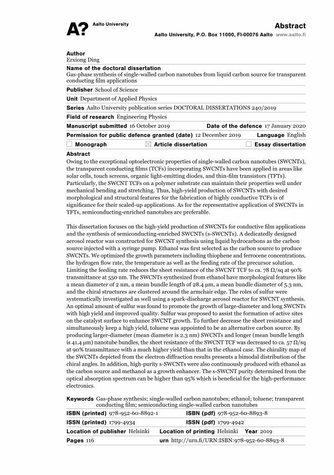
tcartsbA,)sTNCWS( sebutonan nobrac dellaw-elgnis fo seitreporp cinortceleotpo lanoitpecxe eht ot gniwO
ekil saera ni deilppa neeb evah sTNCWS gnitaroprocni )sFCT( smlfi gnitcudnoc tnerapsnart eht .)sTFT( srotsisnart mlfi-niht dna ,sedoid gnittime-thgil cinagro ,sneercs hcuot ,sllec ralos
rednu llew seitreporp rieht niatniam nac etartsbus remylop a no sFCT TNCWS eht ,ylralucitraP derised htiw sTNCWS fo noitcudorp dleiy-hgih ,suhT .gnihcterts dna gnidneb lacinahcem
fo si sFCT evitcudnoc ylhgih fo noitacirbaf eht rof serutaef larutcurts dna lacigolohprom ni sTNCWS fo noitacilppa evitatneserper eht rof sA .snoitacilppa pu-delacs rieht rof ecnacfiingis
.elbareferp era sebutonan dehcirne-gnitcudnocimes ,sTFT
snoitacilppa mlfi evitcudnoc rof sTNCWS fo noitcudorp dleiy-hgih eht no sesucof noitatressid sihT dengised yldetacided A .)sTNCWS-s( sTNCWS dehcirne-gnitcudnocimes fo sisehtnys eht dna
nobrac eht sa snobracordyh diuqil gnisu sisehtnys TNCWS rof detcurtsnoc saw rotcaer losorea ecudorp ot ecruos nobrac eht sa detceles tsrfi saw lonahtE .pmup egnirys a htiw detcejni ecruos
,snoitartnecnoc enecorref dna enehpoiht gnidulcni sretemarap htworg eht dezimitpo eW .sTNCWS .noitulos rosrucerp eht fo etar gnideef eht sa llew sa erutarepmet eht ,etar wofl negordyh eht
%09 ta qs/Ω 87 .ac ot FCT TNCWS eht fo ecnatsiser teehs eht secuder etar gnideef eht gnitimiL ekil serutaef lacigolohprom evah lonahte morf dezisehtnys sTNCWS ehT .mn 055 ta ecnattimsnart
,mn 3.5 fo retemaid eldnub naem a ,mμ 4.82 fo htgnel eldnub naem a ,mn 2 fo retemaid naem a erew ruflus fo selor ehT .egde riahcmra eht dnuora deretsulc era serutcurts larihc eht dna
.sisehtnys TNCWS rof rotcaer losorea egrahcsid-kraps a gnisu llew sa detagitsevni yllacitametsys sTNCWS gnol dna retemaid-egral fo htworg eht etomorp ot dnuof saw ruflus fo tnuoma lamitpo nA
setis evitca fo noitamrof eht tsissa ot desoporp saw rufluS .ytilauq devorpmi dna dleiy hgih htiw dna ecnatsiser teehs eht esaerced rehtruf oT .htworg TNCWS ecnahne ot ecafrus tsylatac eht no yB .ecruos nobrac evitanretla na eb ot detnioppa saw eneulot ,dleiy hgih a peek ylsuoenatlumis
htgnel eldnub naem( regnol dna sTNCWS )mn 3.2 si retemaid naem( retemaid-regral gnicudorp qs/Ω 75 .ac ot desaerced saw FCT TNCWS eht fo ecnatsiser teehs eht ,seldnub ebutonan )mμ 4.14 si fo pam ytilarihc ehT .esac lonahte eht ni taht naht dleiy rehgih hcum a htiw ecnattimsnart %09 ta eht fo noitubirtsid ladomib a stneserp stluser noitcarffid nortcele eht morf detciped sTNCWS eht sa lonahte htiw decudorp ylsuounitnoc osla erew sTNCWS-s ytirup-hgih ,noitidda nI .selgna larihc eht morf denimreted ytirup TNCWS-s ehT .recnahne htworg a sa lonahtem dna ecruos nobrac eht ecnamrofrep-hgih eht rof laicfieneb si hcihw %59 naht rehgih eb nac murtceps noitprosba lacitpo
.scinortcele
sdrowyeK tnerapsnart ;eneulot ;lonahte ;sebutonan nobrac dellaw-elgnis ;sisehtnys esahp-saG sebutonan nobrac dellaw-elgnis gnitcudnocimes ;mlfi gnitcudnoc
)detnirp( NBSI 1-2988-06-259-879 )fdp( NBSI 8-3988-06-259-879
)detnirp( NSSI 4394-9971 )fdp( NSSI 2494-9971
rehsilbup fo noitacoL iknisleH gnitnirp fo noitacoL iknisleH raeY 9102
segaP 611 nru :NBSI:NRU/fi.nru//:ptth 8-3988-06-259-879

i
Acknowledgements
The research work included in this dissertation, supervised by Professor Esko I. Kauppinen, was carried out during 2015-2019 in the NanoMaterials Group at the Department of Applied Physics, Aalto University School of Science. As a continuance of the research work during my Master’s study, I selected the NanoMaterials Group here for deep learning of the same research field. Esko’s acceptance of me joining this group has been greatly appreciated. It is Esko who taught me to concentrate on one research topic in depth for years, which encourages me to do so in future work. Additionally, Esko’s kindness and greetings in Chinese, as well as his energetic spirit, have been motivating me to concentrate on research work. I have learned a lot from my colleagues from different parts of the world, whose comments and guidance have been really valuable to my work which would be much poorer without their help.
My special gratitude goes to Esko who offered me a stage to work here without any financial concerns, and from whom I learned how to pursue my future career devotionally and energetically. Thank you for creating such a positive working environment in which everyone is that helpful in his/her expertise, for bringing me to the conferences from which I could follow the latest research progress and particular thanks for providing opportunities to many activities which have enriched my life in Finland. I also would like to express my gratitude to Dr. Hua Jiang who replied to my inquiries during the application period, guided me upon arriving in Finland. As one of the thesis advisors, Dr. Jiang efficiently provided valuable comments on my publications and dissertation and has been supporting my work all the time. I want to thank Dr. Qiang Zhang, as another thesis advisor, who has been offering useful suggestions and guidance on my experiments as well as comments on the writing. I wish to thank Dr. Ying Tian who taught me to perform optical characterizations and relevant analysis of samples, Dr. Patrik Laiho who established a sample collection system, Dr. Nan Wei who exploited a program for the generation of the chiral map of carbon nanotubes and created a group Wiki, and Dr. Mohammad Tavakkoli from whom I learned electrochemistry knowledge. Peer support and company from doctoral students Aqeel Hussain, Yongping Liao, Saeed Ahmad, Abu Taher Khan, and Nurcin Ugur have been important to me throughout the whole doctoral study. Except for discussions of research work, frequent gathering with you diversified my life as well. La-boratory and administrative supports provided by Timo Kajava, Marita Halme, and Reetta Lesonen have also been helpful to me. I also want to thank many of

ii
my friends studying or working at Aalto University. Thank you for your com-pany in different social activities which have been always joyful for me.
The dissertation pre-examiners Professor Kaili Jiang and Professor John Hart are greatly acknowledged for their insightful comments to polish the final version of this dissertation. I am also grateful to Professor Milo Shaffer for accepting to be the opponent.
Last but not least, my most sincere appreciation goes to my family, especially my parents. Thank you for believing and supporting me at any time. I could not feel assured of my work and have the achievements without your under-standing. Thanks to the playing around of my lovely nephew and niece who drove your loneliness away. Espoo, October 2019 Erxiong Ding
iii
Contents
Acknowledgements................................................................. i
Contents ............................................................................... iii
List of Abbreviations and Symbols......................................... v
List of Publications ............................................................... vi
Author’s Contribution ......................................................... vii
Other featured publications................................................ viii
1. Introduction .................................................................... 1
2. Single-walled carbon nanotubes ..................................... 4
2.1 Morphology and structure ......................................................... 4
2.2 Electronic properties ................................................................. 5
2.3 Optical properties ...................................................................... 7
2.3.1 Optical absorption .................................................................. 7
2.3.2 Raman .................................................................................... 8
2.4 Synthesis process ....................................................................... 9
2.5 Transparent conducting film .................................................... 11
3. Methods ......................................................................... 15
3.1 Reactor design and setup.......................................................... 15
3.2 SWCNT synthesis and TCF fabrication .................................... 16
3.2.1 Materials ............................................................................... 16
3.2.2 Ethanol as the carbon source ................................................ 17
3.2.3 SWCNT synthesis in a spark-discharge reactor .................... 17
3.2.4 Toluene as the carbon source ................................................ 17
3.2.5 Synthesis of semiconducting-enriched SWCNTs .................. 17
3.3 Optical spectroscopy characterizations ....................................18
3.3.1 Absorption .............................................................................18
3.3.2 Raman ...................................................................................18
3.4 Microscopy characterizations ...................................................18
3.4.1 Scanning electron microscopy ..............................................18
3.4.2 Atomic force microscopy ....................................................... 19
3.4.3 Transmission electron microscopy ....................................... 19
iv
3.5 Doping of SWCNT films .......................................................... 20
3.6 Measurement of sheet resistances .......................................... 20
4. Results ........................................................................... 21
4.1 Testing new reactor .................................................................. 21
4.2 Optimizing parameters after adding thiophene and H2 .......... 23
4.2.1 The effect of thiophene concentration .................................. 23
4.2.2 The effect of ferrocene concentration ................................... 25
4.2.3 The effects of H2 and temperature ........................................ 26
4.2.4 The effect of the feeding rate of precursor solution ............. 27
4.3 Chiral indices of the SWCNTs synthesized from ethanol ........ 32
4.4 Independent study on the roles of sulfur ................................. 35
4.5 Toluene as the carbon source for nanotube synthesis ............. 37
4.5.1 Controlling the quality of SWCNTs ..................................... 38
4.5.2 Tuning the diameters of SWCNT bundles ........................... 40
4.5.3 Enhancing film conductivity by dopant ............................... 41
4.5.4 Comparison of film performance and yield .......................... 42
4.5.5 Chiral indices of the SWCNTs synthesized from toluene ..... 45
4.6 Production of semiconducting-enriched SWCNTs ..................46
4.6.1 The effect of methanol amount ............................................. 47
5. Conclusion and outlook ................................................ 49
References ........................................................................... 52
Appendices Publications -

v
List of Abbreviations and Symbols
AFM atomic force microscope or microscopy
CVD chemical vapor deposition
CNT carbon nanotube
EDS Energy-dispersive X-ray spectroscopy
FCCVD floating catalyst chemical vapor deposition
FT-IR Fourier-transform infrared spectroscopy
ITO indium tin oxide
m-SWCNT metallic single-walled carbon nanotube
OLED organic light-emitting diode
PET polyethylene terephthalate
RBM radial breathing mode
RMS root-mean-square
SEM scanning electron microscope or microscopy
s-SWCNT semiconducting single-walled carbon nanotube
SWCNT single-walled carbon nanotube
TCF transparent conducting film
TEM transmission electron microscopy or microscope
TFT thin-film transistor
TG thermogravimetric
T% optical transmittance in percents
UV-Vis-NIR ultraviolet-visible-near infrared spectroscopy
XPS X-ray photoelectron spectroscopy
1D one-dimensional

vi
List of Publications
This doctoral dissertation consists of a summary and the following publica-tions which are referred to in the text by their Roman numerals. I. Ding, Er-Xiong; Jiang, Hua; Zhang, Qiang; Tian, Ying; Laiho, Patrik; Hussain, Aqeel; Liao, Yongping; Wei, Nan; Kauppinen, Esko I. 2017. Highly conductive and transparent single-walled carbon nanotube thin films from ethanol by floating catalyst chemical vapor deposition. The Royal Society of Chemistry. Nanoscale, volume 9, issue 44, pages 17601-17609. ISSN 2040-3372. DOI: 10.1039/c7nr05554d.
II. Ding, Er-Xiong; Zhang, Qiang; Wei, Nan; Khan, Abu Taher; Kauppinen, Esko I. 2018. High-performance single-walled carbon nanotube transparent conducting film fabricated by using low feeding rate of ethanol solution. The Royal Society Publishing. Royal Society open science, volume 5, issue 6, article number 180392 (8 pages). ISSN 2054-5703. DOI: 10.1098/rsos.180392.
III. Ahmad, Saeed; Ding, Er-Xiong; Zhang, Qiang; Jiang, Hua; Sainio, Jani; Tavakkoli, Mohammad; Hussain, Aqeel; Liao, Yongping; Kauppinen, Esko I. 2019. Roles of sulfur in floating-catalyst CVD growth of single-walled carbon nanotubes for transparent conductive film applications. Elsevier. Chemical Engineering Journal, volume 378, article number 122010 (8 pages). ISSN 1385-8947. DOI: 10.1016/j.cej.2019.122010.
IV. Ding, Er-Xiong; Hussain, Aqeel; Ahmad, Saeed; Zhang, Qiang; Liao, Yongping; Jiang, Hua; Kauppinen, Esko I. 2019. High-performance transpa-rent conducting films of long single-walled carbon nanotubes synthesized from toluene alone. Springer, Nano Research, 9 pages. ISSN 1998-0124. DOI: 10.1007/s12274-019-2581-7.
vii
Author’s Contribution
Publication I: Highly conductive and transparent single-walled carbon nanotube thin films from ethanol by floating catalyst chemical vapor deposi-tion The author designed and built the aerosol reactor for carbon nanotube synthe-sis together with the author’s supervisor, carried out all the experiments, ana-lyzed the data and wrote the manuscript. The co-authors polished the interpre-tation of the figures and helped to finalize the manuscript.
Publication II: High-performance single-walled carbon nanotube transpa-rent conducting film fabricated by using low feeding rate of ethanol solution The author carried out all the experiments except AFM characterization, inter-preted the results and wrote the manuscript. The third and fourth authors con-tributed to AFM characterization. All co-authors commented on the analysis of the results and the manuscript.
Publication III: Roles of sulfur in floating-catalyst CVD growth of single-walled carbon nanotubes for transparent conductive film applications The author helped to collect samples, jointly carried out the electron diffrac-tion work and analysis as well as the mechanism explanation of the sulfur role. The author also participated in data analysis and manuscript polishing.
Publication IV: High-performance transparent conducting films of long sin-gle-walled carbon nanotubes synthesized from toluene alone The author performed most of the experiments with the guide from the cor-responding authors, analyzed the results and wrote the manuscript. The second and third authors helped to collect samples and Raman spectra. The co-authors commented on the analysis of results and the manuscript.
viii
Other featured publications
The author has also contributed to the following publications:
Ding, Er-Xiong; Khan, Abu Taher; Wei, Nan; Zhang, Qiang; Ahmad, Saeed; Hussain, Aqeel; Jiang, Hua; Kauppinen, Esko I. 2019. Continuous production of semiconducting-enriched single-walled carbon nanotubes for high-performance electronics. Manuscript in preparation, 2019.
Hussain, Aqeel; Ding, Er-Xiong; McLean Ben; Mustonen, Kimmo; Ahmad, Saeed; Page J. Alister; Zhang, Qiang; Kotakoski, Jani; Kauppinen, Esko I. 2019. Scalable growth of single-walled carbon nanotubes with highly uniform structure. Submitted to the journal Nanoscale Horizons in the year 2019 (16 pages).
Hussain, Aqeel; Liao, Yongping; Zhang, Qiang; Ding, Er-Xiong; Laiho, Patrik; Ahmad, Saeed; Wei, Nan; Tian, Ying; Jiang, Hua; Kauppinen, Esko I. 2018. Floating catalyst CVD synthesis of single walled carbon nanotubes from ethylene for high performance transparent electrodes. The Royal Society of Chemistry. Nanoscale, volume 10, issue 20, pages 9752-9759. ISSN 2040-3372. DOI: 10.1039/c8nr00716k.
Inani, Heena; Mustonen, Kimmo; Markevich, Alexander; Ding, Er-Xiong; Tripathi, Mukesh; Hussain, Aqeel; Mangler, Clemens; Kauppinen, Esko I.; Susi, Toma; Kotakoski, Jani. 2019. Silicon substitution in nanotubes and graphene via intermittent vacancies. American Chemical Society. The Journal of Physical Chemistry C, volume 123, issue 20, pages 13136-13140. ISSN 1932-7447. DOI: 10.1021/acs.jpcc.9b01894.
Ahmad, Saeed; Liao, Yongping; Hussain, Aqeel; Zhang, Qiang; Ding, Er-Xiong; Jiang, Hua; Kauppinen, Esko I. 2019. Systematic investigation of the catalyst composition effects on single-walled carbon nanotubes synthesis in floating-catalyst CVD. Elsevier. Carbon, volume 149, pages 318-327. ISSN 0008-6223. DOI: 10.1016/j.carbon.2019.04.026.
Laiho, Patrik ; Rafiee, Mahdi; Liao, Yongping; Hussain, Aqeel; Ding, Er-Xiong; Kauppinen, Esko I. 2018. Wafer-scale thermophoretic dry deposition of single-walled carbon nanotube thin films. American Chemical Society. ACS Omega, volume 3, issue 1, pages 1322-1328. ISSN 2470-1343. DOI: 10.1021/acsomega.7b01869.

ix
Mustonen, Kimmo; Markevich, Alexander; Tripathi, Mukesh; Inani, Heena; Ding, Er-Xiong; Hussain, Aqeel; Mangler, Clemens; Kauppinen, Esko I.; Kotakoski, Jani; Susi, Toma. 2019. Electron-beam manipulation of silicon impurities in single-walled carbon nanotubes. Wiley. Advanced Functional Materials, article number 1901327 (7 pages). ISSN 1616-3028. DOI: 10.1002/adfm.201901327.
Liao, Yongping; Hussain, Aqeel; Laiho, Patrik; Zhang, Qiang; Tian, Ying; Wei, Nan; Ding, Er-Xiong; Khan, Sabbir A.; Nguyen, Nguyen Ngan; Ahmad, Saeed; Kauppinen, Esko I. 2018. Tuning geometry of SWCNTs by CO2 in floating catalyst CVD for high performance transparent conductive films. Wiley. Advanced Materials Interfaces, volume 5, issue 23, article number 1801209 (10 pages). ISSN 2196-7350. DOI: 10.1002/admi.201801209.
Ahmad, Saeed; Laiho, Patrik; Zhang, Qiang; Jiang, Hua; Hussain, Aqeel; Liao, Yongping; Ding, Er-Xiong; Wei, Nan; Kauppinen, Esko I. 2018. Gas phase synthesis of metallic and bimetallic catalyst nanoparticles by rod-to-tube type spark discharge generator. Elsevier. Journal of Aerosol Science, volume 123, pages 208-218. ISSN 0021-8502. DOI: 10.1016/j.jaerosci.2018.05.011.
Wei, Nan; Laiho, Patrik; Khan, Abu Taher; Hussain, Aqeel; Lyuleeva, Alina; Ahmad, Saeed; Zhang, Qiang; Liao, Yongping; Tian, Ying; Ding, Er-Xiong; Ohno, Yutaka; Kauppinen, Esko I. 2019. Fast and ultraclean approach for measuring the transport properties of carbon nanotubes. Wiley. Advanced Functional Materials, article number 1907150 (9 pages). ISSN 1616-3028. DOI: 10.1002/adfm.201907150.


1
1. Introduction
Carbon nanotubes (CNTs), especially single-walled CNTs (SWCNTs), are at-tracting much attention owing to their outstanding electrical, optical and me-chanical properties, and have been utilized in various fields accordingly[1]. The overlap of randomly oriented or aligned CNTs makes a network named CNT film which is generally transparent and conductive and can be applied directly into areas as solar cells[2], touch screens[3] and organic light-emitting diodes[4]. A CNT film on a flexible and/or stretchable substrate, e.g., polye-thylene terephthalate (PET), polydimethylsiloxane, preserves the properties very well under mechanical bending or stretching, thus exhibits a great poten-tial in flexible and transparent electronics[5] which are expected to be com-mercialized in the near future (there already exist some companies focusing on flexible and transparent electronics based on CNT films, e.g., Canatu Oy in Finland, Tsinghua-Foxconn Nanotechnology Research Center in China). We have developed a dry technique to fabricate SWCNT thin films in principle onto any substrate, which can retain the pristine morphology/structure of SWCNTs to demonstrate the properties of as-synthesized SWCNTs[6]. The SWCNTs produced by an aerosol-based or floating catalyst chemical vapor deposition (FCCVD) method can be deposited onto a membrane filter via gas- phase filtration, and be real-time monitored using the aerosol measurement equipment, which provides instant feedback for optimizing experimental pa-rameters. Besides, the size and thickness of an SWCNT film can be readily con-trolled by the filter size and collection time, respectively. The dry fabrication of SWCNT thin films avoids the irreversible change of morphology/structure including shortening of CNTs and wrapping of residue dispersant which gen-erally exists in those films prepared by the solution-evolved method[7]. As a result, the performance of dry-deposited SWCNT film-based thin-film transis-tor (TFT)[8] prevails over that of TFT fabricated from the solution-processed SWCNTs. Therefore, the FCCVD method was adopted to produce SWCNTs throughout the research topics presented in this dissertation.
To synthesize SWCNTs by the FCCVD method, carbon and catalyst precur-sors are needed. Compared with toxic carbon monoxide (CO), flammable and explosive gaseous hydrocarbons as methane (CH4), ethylene (C2H4), ethanol (C2H6O) has the advantages of low-cost, relative non-toxicity, easy accessibility and is a clean energy source, thus has been frequently employed as the carbon source for SWCNT synthesis. CNT fibers directly spun from the outlet of an FCCVD reactor have been reported using ethanol as the carbon source[9]. However, transparent conducting films (TCFs) consisting of SWCNTs synthe-

Introduction
2
sized from ethanol have not been fabricated yet. Although several references on FCCVD-produced SWCNTs with ethanol as the carbon source can be found[10–14], the characterizations were insufficient for detailed analysis, especially the chiral structures of SWCNTs need to be studied in depth. Herein, ethanol was used as the carbon source to produce SWCNTs in an aerosol reac-tor for the fabrication of TCFs. By optimizing the growth parameters, we fabri-cated AuCl3-doped SWCNT TCFs with a sheet resistance of ca. 78 Ω/sq at 90% transmittance (T) at 550 nm. Meanwhile, the morphologies and structures of as-produced SWCNTs were studied in detail. Particularly, the chiral indices, (n,m)s, of SWCNTs were determined by the electron diffraction technique, generating chirality maps which provide a comprehensive understanding of SWCNTs.
For SWCNT synthesis, a promoter like sulfur or water added into the synthe-sis reactor significantly affects SWCNT growth. For instance, sulfur has been frequently employed as a growth promoter in the FCCVD method for SWCNT synthesis. The addition of sulfur was found to increase nanotube yield, diame-ter, length and to tune the chirality distribution of SWCNTs. However, the roles of sulfur in regulating the morphological and structural features of SWCNTs are not clear enough. Here, we independently studied the roles of sulfur in SWCNT growth by using the spark-discharge-produced iron and co-balt particles as the catalysts and ethylene as the carbon source for SWCNT synthesis in an FCCVD reactor. The effects of sulfur on SWCNT yield, diameter, length, chiralities as well as the optoelectronic performance of SWCNT films were systematically investigated. We suggested that an optimal amount of sul-fur can promote the formation of active sites on the catalyst surface to enhance SWCNT growth.
Except for ethanol as the carbon source, toluene (C7H8) was also adopted to grow SWCNTs for the fabrication of TCFs with enhanced optoelectronic per-formance. Toluene has been selected as the carbon source to synthesize CNTs for spinning CNT fibers which require high-yield production of CNTs[15–17]. Thus, compared with that in ethanol case, the SWCNT yield may be increased further if toluene is selected as the carbon source here, meanwhile keeping the competitive optoelectronic performance of TCFs. Moreover, in contrast to ethanol, toluene is an aromatic compound that excludes the effect of the oxy-gen-containing group on SWCNT growth, which is helpful for the mechanism study of chirality distribution. By producing large-diameter (mean diameter is 2.3 nm) SWCNTs and long (mean length is 41.4 μm) nanotube bundles, we achieved a low sheet resistance of ca. 57 Ω/sq at 90% T for the SWCNT TCFs. For structural analysis of the SWCNTs, a chirality map of the SWCNTs was depicted from the electron diffraction results.
Ethanol has been frequently selected as the carbon source to synthesize se-miconducting SWCNTs (s-SWCNTs) as well. Due to the existence of variable band gaps, s-SWCNTs have been aggressively applied in the semiconductor fields, e.g., digital electronics[18], thermoelectric generators[19], photovol-taics[20] confirmed by the corresponding proof-of-concept demonstrations. The purities of s-SWCNTs higher than 99.9% have been claimed using both

Introduction
3
solution separation[21] and substrate CVD growth[22] methods. Nevertheless, the lengths of solution-sorted s-SWCNTs are limited roughly in the range of 0.5~2 μm[21], and the dispersant or polymer is hard to be completely removed. The s-SWCNTs directly grown on a substrate have to be post-transferred to a target substrate and suffer from low yield. Consequently, large-scale fabrica-tion of ultrahigh-performance electronics based on the s-SWCNTs produced by those two methods is still under investigation. Combining the FCCVD me-thod with ethanol being the carbon source, in this dissertation, we have pre-sented the continuous production of semiconducting-enriched SWCNTs.
This dissertation consists of five chapters. In Chapter 1, the research moti-vation and main conclusive results are summarized. Chapter 2 introduces fundamental knowledge of SWCNTs, i.e., structural, electrical and optical properties, as well as basic properties and figure of merit of SWCNT TCFs. Chapter 3 describes the experimental methods to synthesize SWCNTs, the fabrication of SWCNT TCFs, film doping process and characterization tech-niques. The result and discussion part locates in Chapter 4 in which reactor design, optimization of growth parameters and interpretation of results are included. Finally, Chapter 5 concludes the main results of the studies con-tained in the dissertation and discusses possible directions for the future re-search of SWCNT TCFs and s-SWCNTs.
4
2. Single-walled carbon nanotubes
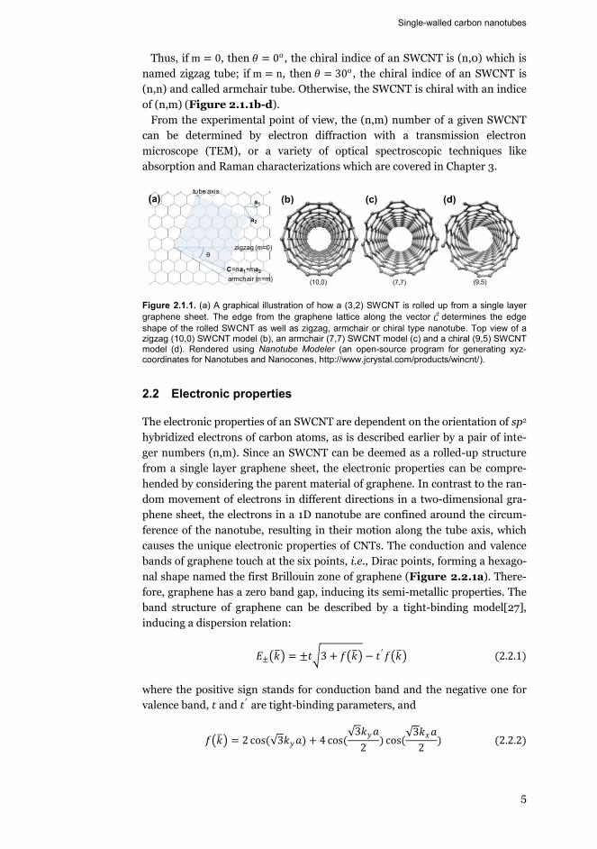
2.1 Morphology and structure
For easy understanding, an single-walled carbon nanotube (SWCNT) can be visually thought of as a one-dimensional (1D) cylindrical hollow structure rolled-up from a single layer graphene sheet (Figure 2.1.1a), though in an actual case no SWCNT grows in this way. The diameter of an SWCNT generally situates in the range of 0.7~2.5 nm, depending on the method used to synthesize nanotubes. An SWCNT with the smallest diameter of 0.3 nm has been found inside a multi-walled CNT through high-resolution transmission electron microscopy (TEM) obervation[23]. On the other hand, an SWCNT with a diameter approaching 6 nm was also obtained by the laser vaporization growth method[24]. Except for the growth method, the experimental parameters utilized in an specific synthesis technique can also affect the diameters of SWCNTs. For instance, we have found that the mean diameter of SWCNTs can be tuned by the concentration of hydrogen, and larger-diameter SWCNTs were synthesized with a higher flow rate of hydrogen[25]. Regarding the length of an SWCNT, the typical value spans from hundreds of nanometers to dozens of micrometers, which is also dependent on the growth method and experimental parameters.
According to the rolling-up illustration, an SWCNT can be described by a chiral vector[26]:
where and are the unit vectors of the graphene hexagonal lattice. The lengths of unit vectors and are calculated as follows:
, where is the distance between the nearest neighboring carbon atoms, 0.142 nm. Thus, the diameter of an SWCNT is determined by:
The angle named chiral angle is defined by the formula:
Single-walled carbon nanotubes
5
Thus, if , then , the chiral indice of an SWCNT is (n,0) which is named zigzag tube; if , then , the chiral indice of an SWCNT is (n,n) and called armchair tube. Otherwise, the SWCNT is chiral with an indice of (n,m) (Figure 2.1.1b-d).
From the experimental point of view, the (n,m) number of a given SWCNT can be determined by electron diffraction with a transmission electron microscope (TEM), or a variety of optical spectroscopic techniques like absorption and Raman characterizations which are covered in Chapter 3.
Figure 2.1.1. (a) A graphical illustration of how a (3,2) SWCNT is rolled up from a single layer graphene sheet. The edge from the graphene lattice along the vector determines the edge shape of the rolled SWCNT as well as zigzag, armchair or chiral type nanotube. Top view of a zigzag (10,0) SWCNT model (b), an armchair (7,7) SWCNT model (c) and a chiral (9,5) SWCNT model (d). Rendered using Nanotube Modeler (an open-source program for generating xyz-coordinates for Nanotubes and Nanocones, http://www.jcrystal.com/products/wincnt/).
2.2 Electronic properties
The electronic properties of an SWCNT are dependent on the orientation of sp2 hybridized electrons of carbon atoms, as is described earlier by a pair of inte-ger numbers (n,m). Since an SWCNT can be deemed as a rolled-up structure from a single layer graphene sheet, the electronic properties can be compre-hended by considering the parent material of graphene. In contrast to the ran-dom movement of electrons in different directions in a two-dimensional gra-phene sheet, the electrons in a 1D nanotube are confined around the circum-ference of the nanotube, resulting in their motion along the tube axis, which causes the unique electronic properties of CNTs. The conduction and valence bands of graphene touch at the six points, i.e., Dirac points, forming a hexago-nal shape named the first Brillouin zone of graphene (Figure 2.2.1a). There-fore, graphene has a zero band gap, inducing its semi-metallic properties. The band structure of graphene can be described by a tight-binding model[27], inducing a dispersion relation:
where the positive sign stands for conduction band and the negative one for valence band, and are tight-binding parameters, and
armchair (n=m)
zigzag (m=0)
C=na1+ma2
tube axisa1
a2
zθ
(a) (b) (c) (d)
(10,0) (7,7) (9,5)

Single-walled carbon nanotubes
6
where is the graphene lattice constant. In an SWCNT, the wave vector is quantized along the circumference of the
tube because of the periodic boundary condition[28]:
where is the chiral vector, is an integer. These two parameters define the allowed states of an SWCNT as well as the parallel lines in the reciprocal space. By slicing the band structure of graphene, each line generates an energy sub-band. In addition, the position of the line determines the metallicity of the SWCNT. If the line goes through the Dirac points of graphene, then the SWCNT is called metallic nanotube (Figure 2.2.1b). A semiconducting nano-tube is defined when no line passes through the points (Figure 2.2.1c). The (n,m) number determines whether the line inserts the points or not. If
, d is an integer, then an SWCNT behaves metallic properties, otherwise, it is a semiconductor in which exists a band gap between the conduction and valence bands. The band gap of a semiconducting SWCNT is inversely proportionally to its diameter, approximately following the empirical fomular[28]:
where d is the diameter of the SWCNT. It has also been predicted that small band gaps may exist in (n,0) metallic SWCNTs, due to the curvature-induced hybridization of s and p orbitals[29]. However, (n,n) armchair nanotubes are believed to be truly metallic.
In an SWCNT, the density of states (DOS) follows its electronic band struc-ture and exhibits the van Hove singularities characteristic of 1D structure.
Figure 2.2.1. (a) Top: The band structure of graphene. The conduction and valence bands touch at the six K-points in the Fermi energy plane. Bottom: The first Brillouin zone of graphene. The black lines are cuts of the graphene band structure and stand for the allowed states of a(3,3) nanotube. Reproduced from Ref. [30] with permission. Copyright 2002, American Chemi-cal Society. (b) For the metallic nanotubes, the line goes through a K point (corner of the hex-agonal) at the Fermi energy of graphite. (c) For the semiconducting nanotubes, the line does not pass through the K point. (b) and (c) are reproduced from Ref. [31] with permission. Copy-right 2000, American Physical Society.
(a) (b) (c)
Single-walled carbon nanotubes
7
2.3 Optical properties
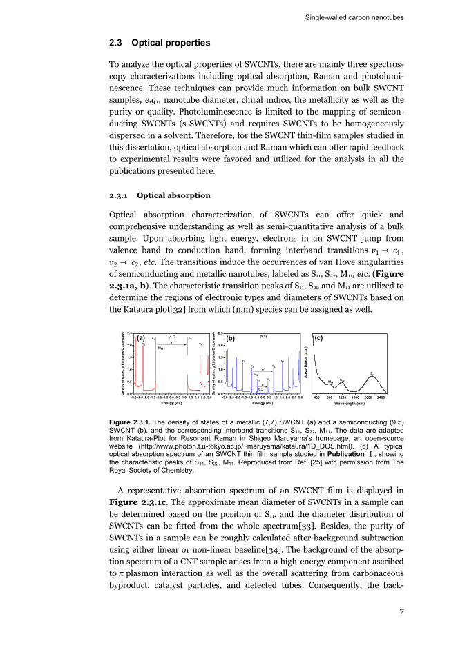
To analyze the optical properties of SWCNTs, there are mainly three spectros-copy characterizations including optical absorption, Raman and photolumi-nescence. These techniques can provide much information on bulk SWCNT samples, e.g., nanotube diameter, chiral indice, the metallicity as well as the purity or quality. Photoluminescence is limited to the mapping of semicon-ducting SWCNTs (s-SWCNTs) and requires SWCNTs to be homogeneously dispersed in a solvent. Therefore, for the SWCNT thin-film samples studied in this dissertation, optical absorption and Raman which can offer rapid feedback to experimental results were favored and utilized for the analysis in all the publications presented here.
2.3.1 Optical absorption
Optical absorption characterization of SWCNTs can offer quick and comprehensive understanding as well as semi-quantitative analysis of a bulk sample. Upon absorbing light energy, electrons in an SWCNT jump from valence band to conduction band, forming interband transitions ,
, etc. The transitions induce the occurrences of van Hove singularities of semiconducting and metallic nanotubes, labeled as S11, S22, M11, etc. (Figure 2.3.1a, b). The characteristic transition peaks of S11, S22 and M11 are utilized to determine the regions of electronic types and diameters of SWCNTs based on the Kataura plot[32] from which (n,m) species can be assigned as well.
Figure 2.3.1. The density of states of a metallic (7,7) SWCNT (a) and a semiconducting (9,5) SWCNT (b), and the corresponding interband transitions S11, S22, M11. The data are adapted from Kataura-Plot for Resonant Raman in Shigeo Maruyama’s homepage, an open-source website (http://www.photon.t.u-tokyo.ac.jp/~maruyama/kataura/1D_DOS.html). (c) A typical optical absorption spectrum of an SWCNT thin film sample studied in Publication , showing the characteristic peaks of S11, S22, M11. Reproduced from Ref. [25] with permission from The Royal Society of Chemistry.
A representative absorption spectrum of an SWCNT film is displayed in Figure 2.3.1c. The approximate mean diameter of SWCNTs in a sample can be determined based on the position of S11, and the diameter distribution of SWCNTs can be fitted from the whole spectrum[33]. Besides, the purity of SWCNTs in a sample can be roughly calculated after background subtraction using either linear or non-linear baseline[34]. The background of the absorp-tion spectrum of a CNT sample arises from a high-energy component ascribed to plasmon interaction as well as the overall scattering from carbonaceous byproduct, catalyst particles, and defected tubes. Consequently, the back-
-3.0 -2.5 -2.0 -1.5 -1.0 -0.5 0.0 0.5 1.0 1.5 2.0 2.5 3.00.0
0.5
1.0
1.5
2.0
2.5
e-
M11
c1v1
Den
sity
of s
tate
s, g
(E) (
stat
es/C
ato
ms/
eV)
Energy (eV)
v2 c2
(7,7)
-3.0 -2.5 -2.0 -1.5 -1.0 -0.5 0.0 0.5 1.0 1.5 2.0 2.5 3.00.0
0.5
1.0
1.5
2.0
2.5
e-
e-
S11
S22
c3v3
c1
v2
v1
Den
sity
of s
tate
s, g
(E) (
stat
es/C
ato
ms/
eV)
Energy (eV)
c2
(9,5)(a) (b)
400 800 1200 1600 2000 2400
M11
S11
Abs
orba
nce
(a.u
.)
Wavelength (nm)
S22
(c)

Single-walled carbon nanotubes
8
grounds of CNT samples prepared by different methods can be significantly varied. As for the accurate assignment of chiral indices of SWCNTs, one has to carefully prepare solution samples for absorption measurement to obtain the finely resolved transition peaks of individual nanotubes. However, the absorp-tion spectrum of SWCNTs in the form of a thin film always present broad tran-sition peaks under which many (n,m) species are overlapped. Numerical fitting with special care of the spectrum could result in some chiral indices of SWCNTs, though there always exist some variations depending on the fitting code used[35,36]. Except for those transition peaks, a strong plasmon peak located around 250 nm, i.e., ~4.9 eV, also appears in the absorption spectrum of a CNT sample. The plasmon resonance peak is generally believed to origi-nate from the M point in the Brillouin zone of graphene lattice[37]. In practice, the locations of the transition peaks might be shifted by the curvature-induced energy variation[38], the interactions with the environment and nanotube bundling. Among them, the bundling could induce redshifts, e.g., tens of meV, of transition peaks of SWCNTs, which can be understood as a result of the di-electric screening by adjacent nanotubes[39].
2.3.2 Raman
Resonant Raman spectroscopy characterization is also a non-destructive me-thod to provide fine features of SWCNTs. Raman spectroscopy is based on the inelastic Raman scattering of phonons related to the vibrational states in a molecule. In a normal case, the probability of inelastic scattering is rather low, since the electronic transition occurs to a virtual state with a short lifetime. However, the probability is significantly increased if the energy of incident phonon or the emitted phonon coincides with the energy discrepancy of the valence and conduction bands[40]. This process is called Raman resonance phenomenon. One typical Raman spectrum of SWCNTs is displayed in Figure 2.3.2b.
Figure 2.3.2. (a) The Kataura plot showing the optical transition energy Eii of SWCNTs. The blue and red dots stand for semiconducting and metallic SWCNTs, respectively. The family number (2n+m) and excitation wavelength (or energy) are also indicated. Data were adapted from [33]. Copyright 2010, American Chemical Society. (b) A representative Raman spectrum of an SWCNT thin film sample on a quartz substrate similar to those studied in Publication . The wavelength of the excitation laser is 633 nm.
100 150 200 250 300 3501.0
1.2
1.4
1.6
1.8
2.0
2.2
2.4
2.6
49
46
43
4040
37
50
4346
19
22
3835
32
29
36
1718
33
3027
24
26
23
2120
3633
30
27
1922
25
Raman shift (cm-1)
Ener
gy (e
V)
dt(nm)
49
37 488 nm514 nm
633 nm
785 nm
2.4 2 1.6 1.2 0.845
51
2831
34
3235
48
100 200 300 1200130014001500160017001800
RBM
G-
G+
D
Inte
nsity
(a.u
.)
Raman shift (cm-1)
633 nm(a)
(b)
Single-walled carbon nanotubes
9
Typically, the Raman spectrum of SWCNTs is characterized by the radial breathing mode (RBM) and the graphitic (G) mode. The RBM is a bond-stretching out-of-plane phonon mode for which carbon atoms move in the radial direction. The RBM frequency ( ) usually situates in the range of 100~350 cm-1 and is inversely proportional to the nanotube diameter following the empirical formula[33]:
where is the diameter of an SWCNT, and are two expe-rimentally obtained constants for SWCNT thin-film samples. It should be mentioned that some other formulae have also been put forward in specific situations[41] and small corrections to the empirical parameters come from substrate effect and tube-tube interactions. Therefore, the diameters and chir-al indices of resonant SWCNTs can be determined from RBM peaks based on the Kataura plot (Figure 2.3.2a). It is worth noting that even though Raman has been considered to be one of the most important routes for nanotube cha-racterization, one has to adopt multiple excitation wavelengths to excite a sta-tistically reliable (n,m) species in an SWCNT sample, since one laser can only excite a few certain SWCNTs which locate in the resonance energy range[42]. Furthermore, the intensity ratio of the RBM to G modes is highly chiral angle and mode dependent[43]. The nanotube bundling was also found to affect the frequencies of RBM peaks[44,45]. Accordingly, Raman alone cannot be used to reliably determine the (n,m) distribution of an unknown SWCNT sample.
The G band located around 1580 cm-1 in a Raman spectrum is related to tan-gential mode vibrations of the carbon atoms. The G band of SWCNTs normally consists of two sub-bands, higher frequency G+ mode which comes from the vibrations along the tube axis, and lower frequency G- mode that originates from the vibrations in the circumferential direction. The splitting of G band is caused by the curvature-induced energy difference between the axis and cir-cumference in-plane vibration modes. The G- mode is frequently used to dis-tinguish electronic types of SWCNTs. s-SWCNTs are characterized by Lorent-zian line shape and the metallic counterparts generate a broad Breit-Wigner-Fano (BWF) line shape[40].
Except for those first-order features of RBM and G bands, the Raman spec-trum of CNTs also displays a disorder-induced D band around 1350 cm-1. The D band is associated with the impurities and defects, e.g., catalyst particles, amorphous carbon, defected nanotubes, and thus can be used to evaluate the quality of a CNT sample by calculating the ratio of either peak intensities or integrated peak areas of G and D bands.
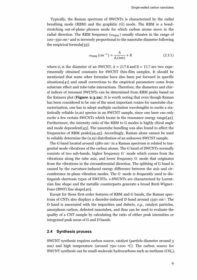
2.4 Synthesis process
SWCNT synthesis requires carbon source, catalyst (particle diameter around 3 nm) and high temperature (around 750~1100 oC). The carbon source for SWCNT synthesis can be small-molecule hydrocarbons such as methane (CH4),
Single-walled carbon nanotubes
10
ethylene (C2H4) and acetylene (C2H2), or carbon monoxide (CO), or liquid hy-drocarbons, e.g., ethanol (C2H6O), toluene (C7H8). Transition metals are the frequently utilized catalysts for nanotube growth, e.g., iron (Fe), cobalt (Co), nickel (Ni), molybdenum (Mo) and their alloys[46]. Copper (Cu) is also a pop-ular catalyst for SWCNT growth[47]. The generally acknowledged formation processes of an SWCNT involve following steps[48], 1) the decomposition of carbon source at high temperature assisted by the catalyst, 2) the permeation of carbon atoms into the catalyst (surface diffusion also happens in some cas-es), 3) the precipitation of carbon atoms on the surface of catalyst particle, forming a carbon cap, 4) the growth of the carbon cap with continuous carbon feeding to form an SWCNT.
Figure 2.4.1. A schematic illustration of the processes for SWCNT synthesis using the substrate CVD method. (1) Spraying coating of the catalyst precursor onto a silicon substrate situated on a hot plate. (2) Reduction of the catalyst precursor to metallic catalyst particles by hydrogen. (3) Introduction of carbon source for SWCNT growth in a tube furnace kept around 900 oC. The schematics are adapted from Ref. [49]. Copyright 2015, Nature publishing group.
The synthesis methods for SWCNTs mainly include high-pressure carbon monoxide (HiPCO)[50], laser ablation[51], arc discharge[52], catalyst-supported chemical vapor deposition (CVD)[53] and floating catalyst CVD (FCCVD)[54]. All the methods have enabled scaled-up production of SWCNTs for commercial applications. Among them, substrate CVD and FCCVD are the most popular methods for mechanism study and application of SWCNTs for the moment. In the substrate CVD method, firstly, the catalyst precursor is prepared by atomic level deposition, e.g., magnetron sputtering, atomic layer deposition, electron beam evaporation, or solution coating, e.g., spray coating, dip coating, spin coating, onto a silicon or quartz substrate. Then, the sub-strate is placed inside a furnace at a set temperature below growth tempera-ture for the reduction of the catalyst precursor by hydrogen. After reducing the catalyst, carbon source together with carrier gas is introduced into the furnace kept at an elevated temperature for a while (usually dozens of minutes) for CNT growth. Then, the introduction of the carbon source is terminated and the substrate is taken out after cooling down the furnace for characterizations. A
Single-walled carbon nanotubes
11
schematic description of the abovementioned processes is demonstrated in Figure 2.4.1. SWCNTs in a vertically[55] or horizontally[56] aligned form are grown by this method. In addition, substrate CVD method is advantageous for chirality- and metallicity-selective growth of SWCNTs since the catalyst can be intentionally designed before the growth for specific targets. On the whole, the substrate CVD is favorable for the mechanism investigation of SWCNT growth, though it suffers from low yield due to the limitation of active catalyst immobi-lized on the substrate, confining their applications in small-scale electronics, e.g., transistors.
By contrast, the FCCVD method enables large-scale production and conti-nuous collection of SWCNTs. In the FCCVD process, carbon precursor and catalyst source (typically ferrocene) are introduced by carrier gas into a reactor set at a target temperature. All the aerosol products are floating in a gas phase and the as-synthesized SWCNTs can be collected from the downstream of the reactor as a form of powder, fiber or film. Compared with the substrate CVD method, the primary difference in the FCCVD method is that the catalyst pre-cursor can be continuously injected into a reactor and the catalyst particles are floating in the gas phase, resulting in short residence times (several seconds) of the products in the growth zone. As a consequence, the FCCVD process is easier to be scaled-up for continuous and industrial-level production. SWCNT fibers and transparent conducting films (TCFs) have been fabricated by the FCCVD method. For instance, Li et al.[57], for the first time, fabricated CNT fibers through continuously withdrawing the product with a rotating spindle from the outlet of an FCCVD reactor. A press-transfer technique has been de-veloped by our group to fabricate SWCNT TCFs with tunable conductivity and transparency[6]. The as-synthesized SWCNTs can be deposited onto a mem-brane filter by gas filtration, forming a thin film of which the size is deter-mined by the collection area of the filter[6,58,59]. We also adopted the FCCVD method to produce SWCNTs studied in the dissertation. The schematic illu-stration of the FCCVD reactor can be found in Chapter 3.1.
2.5 Transparent conducting film
As mentioned in Chapter 1, SWCNTs own unique electrical and optical proper-ties, thus, they can be applied in TCFs. The light can go through the holes with sizes of micrometers in a network formed by SWCNTs which ensure high elec-trical conductivity simultaneously. In contrast to the conventional TCFs made of metal, e.g., silver nanowires, or metal oxide, e.g., indium tin oxide (ITO) film, SWCNT TCFs can maintain their electrical properties quite well under repeated mechanical bending or stretching, making them suitable for the ap-plication in flexible and/or stretchable electronics which could be manufac-tured by the roll-to-roll technique. Moreover, when polyethylene terephthalate (PET) is used as the substrate, SWCNT TCFs have less light reflection com-pared with the commercialized ITO film[3]. ITO also has other disadvantages like the scarcity of indium and high production cost. Therefore, the fabrication

Single-walled carbon nanotubes
12
of large-scale SWCNT TCFs is of great significance for their applications in flexible and/or stretchable electronics.
The fabrication approaches of SWCNT TCFs contain wet and dry processes. The wet process is a solution-evolved method, including vacuum filtration[60], spray coating[61], dip coating[62], spin coating[63], Mayer rod coating[64], etc. In the wet method, firstly, SWCNTs in a powder form are dispersed in a solvent followed by centrifugation to obtain a homogeneous SWCNT ink with a suitable viscosity. Then, the SWCNT ink is utilized to make TCFs by vacuum filtration or coating techniques, after which the TCFs have to be baked in an oven to improve the adhesion with the substrate and be washed repeatedly to remove the dispersant. During those multiple processes, SWCNT lengths can be shortened and the insulating dispersant is hard to be removed completely from the thick bundles (mean bundle diameter can be ca. 10~15 nm). Those negative effects on SWCNTs are the major factors increasing the sheet resis-tances of the SWCNT films fabricated by the wet method. As for the dry me-thod for TCF fabrication, it mainly refers to two routes, i.e., drawing CNT yarns from an aligned CNT array[65] and filter collection of as-synthesized SWCNTs from an FCCVD reactor[6]. The TCF made by drawing yarns from a CNT array is composed of multi-walled CNTs, thus is beyond the scope of the study in this dissertation. The advantages of the FCCVD method for the fabri-cation of SWCNT TCFs include outstanding optoelectronic performance, excel-lent compatibility with the roll-to-roll manufacturing, and the ability to scale-up production. A more detailed introduction of those fabrication techniques can be found in a well-written review article published recently[66]. Schematic illustrations of the fabrication methods of SWCNT TCFs are presented in Fig-ure 2.5.1.
Figure 2.5.1. Schematic illustrations of the fabrication methods for SWCNT TCFs. (a) Vacuum filtration. (b) Spray coating. (c) Dip coating. (d) Spin coating. (e) Mayer rod coating. (f) Drawing CNT yarns from a CNT array. (g) Filter collection of SWCNT film from an FCCVD reactor. The schematics are reproduced with permission from Ref. [66]. Copyright 2016, American Chemical Society.
Before comparing the optoelectronic performance, i.e., sheet resistance ver-sus transmittance demonstrated throughout the dissertation, of SWCNT TCFs
Single-walled carbon nanotubes
13
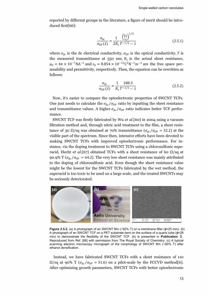
reported by different groups in the literature, a figure of merit should be intro-duced first[66]:
where is the dc electrical conductivity, is the optical conductivity, is the measured transmittance at 550 nm, is the actual sheet resistance,
and are the free space per-meability and permittivity, respectively. Then, the equation can be rewritten as follows:
Now, it’s easier to compare the optoelectronic properties of SWCNT TCFs. One just needs to calculate the ratio by inputting the sheet resistance and transmittance values. A higher ratio indicates better TCF perfor-mance.
SWCNT TCF was firstly fabricated by Wu et al.[60] in 2004 using a vacuum filtration method and, through nitric acid treatment to the film, a sheet resis-tance of 30 Ω/sq was obtained at 70% transmittance ( ) at the visible part of the spectrum. Since then, intensive efforts have been devoted to making SWCNT TCFs with improved optoelectronic performance. For in-stance, via the doping treatment to SWCNT TCFs using a chlorosulfonic supe-racid, Hecht et al.[67] obtained TCFs with a sheet resistance of 60 Ω/sq at 90.9% T ( ). The very low sheet resistance was mainly attributed to the doping of chlorosulfonic acid. Even though the sheet resistance value might be the lowest for the SWCNT TCFs fabricated by the wet method, the superacid is too toxic to be used on a large scale, and the treated SWCNTs may be seriously deteriorated.
Figure 2.5.2. (a) A photograph of an SWCNT film (~92% T) on a membrane filter (ɸ=25 mm). (b) A photograph of an SWCNT TCF on a PET substrate bent on the surface of a quartz tube (ɸ=28 mm) to demonstrate the flexibility of the SWCNT TCF. (b) is presented in Publication . Reproduced from Ref. [68] with permission from The Royal Society of Chemistry. (c) A typical scanning electron microscopy micrograph of the morphology of SWCNT film (~90% T) after ethanol densification.
Instead, we have fabricated SWCNT TCFs with a sheet resistance of 110 Ω/sq at 90% T ( ) on a pilot-scale by the FCCVD method[6]. After optimizing growth parameters, SWCNT TCFs with better optoelectronic
(a) (b) (c)
Single-walled carbon nanotubes
14
performance than the one reported using superacid have been fabricated with high reproductivity[69] and a low sheet resistance of 51 Ω/sq at 90% T ( ). More recently, Jiang et al.[59] released a remarkable result that the SWCNT TCF with an extremely low sheet resistance of 25 Ω/sq at 90% T ( ) was acquired after nitric acid doping. This TCF perfor-mance is comparable with that of ITO film. Therefore, these results have con-firmed that the optoelectronic performance of the SWCNT TCFs fabricated by the FCCVD method is superior to that of the TCFs made by the wet method.
15
3. Methods
3.1 Reactor design and setup
The FCCVD reactor was elaborately designed to synthesize SWCNTs for the formation of uniform films. Herein, laminar flow in the reactor was expected, hence, only a quartz tube (internal diameter is 23 mm, length is 1050 mm) was used without a water-cooling injector which has been adopted for other reac-tors in our laboratory. Ferrocene together with a small amount of thiophene was dissolved in ethanol to form a homogeneous liquid feedstock which can be injected using a syringe pump into a heating line. The syringe pump with a syringe needle diameter of 0.7 mm can precisely control the injection rate of precursor solution which can be evaporated in the heating line at 140 oC. A 10 cm-long stainless steel tube with an inner diameter of 0.5 mm was added to fully mix the gaseous precursors with carrier gas before being introduced into the quartz tube. A stainless steel cone was installed at the inlet part of the quartz tube to ensure the flow gradually expands to form a laminar flow when the vaporized gaseous precursors carried by a mixture of nitrogen (N2) and hydrogen (H2) go through. The mixed gas is heated in the whole heating line to avoid flow recirculation at the inlet part caused by the temperature difference between otherwise introduced cold gas and hot quartz tube. To keep laminar flow passing through the membrane filter for sample collection, at the outlet of the reactor, the upper part of the filter holder was machined to be a cone. All the aerosol products and gases filtrate through the membrane filter while the bypass line is closed when collecting samples. This kind of design for sample collection increases the collection efficiency and uniform SWCNT films can be obtained. A relief valve functionalized automatic release of excess gas was mounted in case of pressure rise inside the quartz tube. Additionally, the ex-haust was purified by a high-efficiency particulate air (HEPA) capsule to re-move ~99.7% particles larger than 0.3 μm and passed through a bubbler vessel containing 2 M/L sodium hydroxide (NaOH) solution to absorb sulfur com-pound decomposed from thiophene before being emitted into the air. The schematic of the FCCVD reactor for SWCNT synthesis is displayed in Figure 3.1.1. Both wall and centerline gas temperatures were measured with 800 standard cubic centimeters (sccm) N2 flushing the quartz tube before starting experiments.

Methods
16
Figure 3.1.1. (a) The flow schematics of the FCCVD reactor for SWCNT synthesis and the formation of SWCNT film on a membrane filter. For clear demonstration, the drawing of a 47 mm filter holder is displayed at the sample collection part. (b) The profiles of the wall and center-line gas temperatures measured with a set temperature of 1000 oC. Carrier gas of 800 sccm N2 was introduced into the reactor from the top of the reactor when measuring temperatures from the bottom. The diameter of the thermocouple tip is 1.5 mm. The schematics and temperature profiles are presented in Publication . Reproduced from Ref. [25] with permission from The Royal Society of Chemistry.
A spark-discharge FCCVD reactor was also utilized for the SWCNT synthesis presented in this dissertation. The main advantage of this reactor is that the catalyst can be pre-made prior to being introduced into the SWCNT synthesis reactor, which enabled us to control the size and composition of the catalyst particles. The catalyst particles were produced inside a rod-to-tube type spark-discharge generator. Briefly, highly pure iron (Fe) or cobalt (Co) rod and tube were utilized as the electrodes. The materials from the electrodes were evapo-rated by applying a high voltage of 2~3 kV across the electrode gap in N2 at-mosphere. The catalyst particles were formed by an evaporation-nucleation-condensation process and were carried into the SWCNT synthesis reactor by N2 flow. Ethylene was selected as the carbon source carried by N2 and H2. The schematics of the spark-discharge reactor for SWCNT synthesis can be found elsewhere[70].
3.2 SWCNT synthesis and TCF fabrication
3.2.1 Materials
Ferrocene (98%) and thiophene (≥99%) were ordered from Sigma-Aldrich. Ethanol (99.5%) was supplied by Altia Oyj, Finland. Toluene (99.7%) and me-thanol (99.9%) were purchased from Alfa Aesar and Acros Organics, respec-tively. Rod and tube iron (99.8%), cobalt (99.95%) electrodes were ordered from Goodfellow in UK. Gold chloride ( 99.99% trace metals basis), acetoni-trile (99.8%) and nitric acid (65%) were from Sigma-Aldrich. AGA in Finland provided hydrogen (99.999%), ethylene (99.999%), diluted H2S (0.01 vol% H2S in N2, 99.999%) and nitrogen (vaporized from liquid nitrogen and purified by an OT3-4 oxygen/moisture trap from Agilent). The membrane filter with a pore size of 0.45 μm was ordered from Merck Millipore, France.
200 300 400 500 600 700 800 900 1000-10
0102030405060708090
100
Axi
al lo
catio
n (c
m)
Temperature (oC)
Twall Tgas
(b)Reactor
top
Reactor bottom
(a)
Methods
17
3.2.2 Ethanol as the carbon source
First, 0.25~0.4 wt% ferrocene together with a small amount of thiophene (mo-lar ratio of S/Fe is in the range of 0.1~0.3) was dissolved in ethanol to form a homogeneous liquid feedstock via two minutes of ultrasonication. Then, the feedstock was loaded into a glass syringe and injected with a syringe pump (NE-1000 series, New Era Pump Systems, USA) at a feeding rate of 4~10 μl/min. The solution evaporated in a heating line at 140 oC enabled by a heat-ing cord and an SDC temperature controller from BriskHeat, USA. The vapo-rized precursors were carried by 600~800 sccm gaseous mixture of N2 and H2 into a vertical aerosol reactor kept at 980~1050 oC. The growth parameters were adjusted in the aforementioned ranges according to the expected results presented in the publications in which specific parameters can be found. As-synthesized SWCNTs were deposited onto a membrane filter placed at the downstream of the reactor to form a thin film by gas-phase filtration. The SWCNT film on the filter was press-transferred onto a quartz slide or silicon substrate for characterizations. The film thickness or transmittance was con-trolled by the collection time.
3.2.3 SWCNT synthesis in a spark-discharge reactor
In all the experiments, the total number concentration and the mobility di-ameter of the catalyst particles were fixed to ~4.3 × 106 cm-3 and ~3.5 nm, re-spectively. 0.1 sccm ethylene and 80 sccm H2 were introduced to the FCCVD reactor set at the temperature of 1050 oC for SWCNT synthesis. As the sulfur source, 0.01 vol% diluted H2S in the flow range of 0~50 sccm, i.e., 0~10 ppm H2S, was used. The pre-made catalyst particles were introduced to the reactor by 370~420 sccm N2. The total flow rate was kept at 500 sccm.
3.2.4 Toluene as the carbon source
An appropriate amount of ferrocene (2~3 wt%) and a small volume of thio-phene (Fe/S molar ratio is in the range of 1.5~3) were dissolved in toluene in a vial. The solution was sonicated for one minute and loaded into a glass syringe with a Teflon plunger tip (Innovative Labor Systeme, Germany). Then, the solution was injected with a syringe pump to a heating line at 130 oC. The va-porizers of the gaseous precursors were carried by N2 (300~500 sccm) and H2 (40~70 sccm) to an elevated temperature (1060~1120 oC) reactor for SWCNT synthesis.
3.2.5 Synthesis of semiconducting-enriched SWCNTs
Ethanol was the carbon source, ferrocene and thiophene were utilized as the catalyst and promoter sources, respectively. A variable amount of methanol (0~36 vol%) was intentionally added to enhance s-SWCNT growth. Based on the work presented in Publication , the experimental parameters were further optimized here. The precursor ethanol solution containing methanol, 0.25 wt% ferrocene and a small amount of thiophene (molar ratio of sulfur to
Methods
18
iron is 0.15) were sonicated for one minute to form a homogeneous solution which was injected at the feeding rate of 1 μl/min into a heating line. The eva-porated precursors in the heating line at 130 oC were carried by 200~300 sccm N2 and an appropriate volume of H2 (7~25 sccm). The temperature of the reac-tor was adjusted in the range of 900~960 oC. As-produced SWCNTs were col-lected at the outlet of the reactor with a patterned 25 mm membrane filter (the collection area was scaled to ca. 5 mm × 5 mm by patterning). The pressure inside the quartz tube was raised due to the usage of the patterned filter. The collection time for the 5 mm × 5 mm film with a transmittance of ca. 95% was around 1~2 hours. The pressure (0~20 KPa) inside the quartz tube was regu-lated by a needle valve (to partially block the exhaust) mounted at the outlet and was measured with a precision digital test gauge (type 2084, Ashcroft, USA).
3.3 Optical spectroscopy characterizations
3.3.1 Absorption
The optical absorption and transmittance spectra of the SWCNT films trans-ferred onto quartz slides (HSQ300, FinnishSpecialGlass, Finland) were meas-ured separately employing a UV-Vis-NIR spectrometer (Agilent Cary 5000) with a wavelength range of 175-3300 nm. A data interval of 1 nm was chosen to ensure a smooth spectrum. Before each measurement, the baseline correction was conducted with two blank quartz slides located in the reference and sam-ple beam paths, respectively. After baseline calibration, the blank slide in the reference beam path was kept to exclude the effect of the substrate while the one in the sample beam path was replaced by a sample slide. The transmit-tance values were read at 550 nm of the transmittance spectra.
3.3.2 Raman
Raman spectra were recorded using a Raman spectrometer (Horiba Jobin-Yvon Labram HR 800) equipped with laser wavelengths of 488 nm, 514 nm, 633 nm, and 785 nm. A 100x magnification objective was selected to minimize the effect of ambient light. A proper filter size was selected to prevent the laser burning of SWCNTs. Every present spectrum was averaged on three spectra collected at different regions (the distance between two locations was set to be longer than the mean length of nanotube bundles to avoid multiple counting of the same tubes) with each laser. All the spectroscopy data were normalized and plotted with Origin.
3.4 Microscopy characterizations
3.4.1 Scanning electron microscopy
Sparsely-distributed SWCNTs were deposited onto a silicon (Si with a 100 nm thick SiO2) substrate by a thermophoretic method[71] for imaging with a scan-
Methods
19
ning electron microscope (SEM, Zeiss Sigma VP) operated at an acceleration voltage of 1 kV using an inlens secondary electron detector. Only the isolated filaments (including individual nanotubes and bundles) whose two ends can be found were taken into account. For simplicity, “bundle length” is used to describe the length of nanotubes in this dissertation. The SWCNT bundle lengths were manually measured using ImageJ from the SEM micrographs. The SWCNT films were densified with ethanol for the observations of surface morphologies.
3.4.2 Atomic force microscopy
A dimension 3100 atomic force microscope (AFM) was employed to scan SWCNT films transferred onto silicon substrates at a tapping mode and Gwyddion was utilized to analyze the AFM images for measuring the surface roughnesses of SWCNT films. SWCNT films were densified with ethanol be-fore AFM characterization.
3.4.3 Transmission electron microscopy
For the TEM observation, SWCNTs were directly deposited onto a lacey car-bon TEM grid situated on a membrane filter. To measure SWCNT bundle di-ameters, the TEM micrographs of the SWCNTs were acquired with a JEOL 2200FS Double Cs-corrected TEM operated at 200 kV.
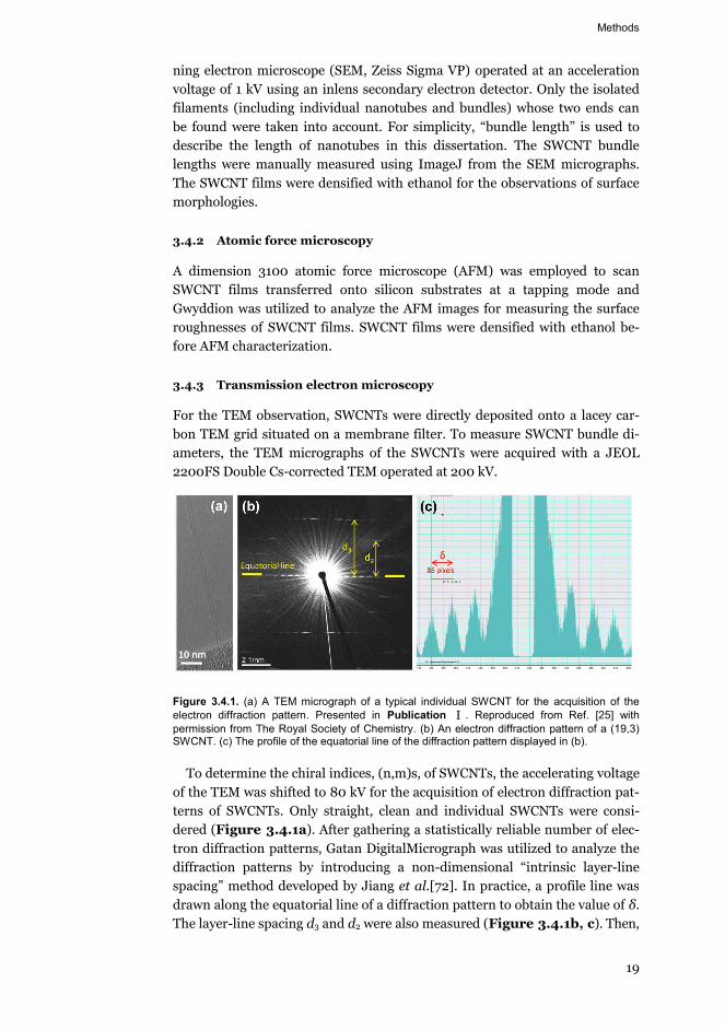
Figure 3.4.1. (a) A TEM micrograph of a typical individual SWCNT for the acquisition of the electron diffraction pattern. Presented in Publication . Reproduced from Ref. [25] with permission from The Royal Society of Chemistry. (b) An electron diffraction pattern of a (19,3) SWCNT. (c) The profile of the equatorial line of the diffraction pattern displayed in (b).
To determine the chiral indices, (n,m)s, of SWCNTs, the accelerating voltage of the TEM was shifted to 80 kV for the acquisition of electron diffraction pat-terns of SWCNTs. Only straight, clean and individual SWCNTs were consi-dered (Figure 3.4.1a). After gathering a statistically reliable number of elec-tron diffraction patterns, Gatan DigitalMicrograph was utilized to analyze the diffraction patterns by introducing a non-dimensional “intrinsic layer-line spacing” method developed by Jiang et al.[72]. In practice, a profile line was drawn along the equatorial line of a diffraction pattern to obtain the value of δ. The layer-line spacing d3 and d2 were also measured (Figure 3.4.1b, c). Then,

Methods
20
the chiral indice, (n,m), of an SWCNT can be calculated based on the three values following the reported method[72].
3.5 Doping of SWCNT films
First, the SWCNT films on membrane filters were press-transferred onto quartz slides. Then, 50 μl of 16 mM fresh gold chloride (AuCl3) solution was drop-casted to each film. The films were washed with pure acetonitrile five minutes later and dried by blowing compressed air prior to sheet resistance measurement. As for HNO3 doping, films were first transferred to PET sub-strates since the films on quartz slides detached upon casting HNO3. Concen-trated HNO3 (65 wt%) was dropped onto nanotube films which were washed with deionized water one minute later. Sheet resistances were measured after drying the films by compressed air. All the doping processes were carried out in a fume hood under ambient conditions.
3.6 Measurement of sheet resistances
Conducting thin films are usually characterized by their sheet resistances, . In a three-dimensional conductor, the resistance can be described as:
where is the resistivity of the conductor, is the length, is the cross-sectional area, is the width, is the thickness.
The sheet resistances of the SWCNT films on quartz slides were measured with a four-point probe (Jandel Engineering Ltd., UK) connected with a digital multimeter (HP 3458A, Hewlett Packard, Agilent) system. The probe consists of four tungsten needles with a separation of 1 mm between each other. The needle tip has a radius of curvature of 100 μm and a loading force of 15 grams per needle. The current is applied to the outer pair needles and voltage can be measured from the inner pair. The sheet resistance value is calculated from the following equation[73]:
where is the value shown on the data readout display, is the final value of
actual sheet resistance. Every data point of sheet resistance was averaged on three measurements at different locations of the same sample. Then, the data points were fitted based on an empirical formula described elsewhere[6].
21
4. Results
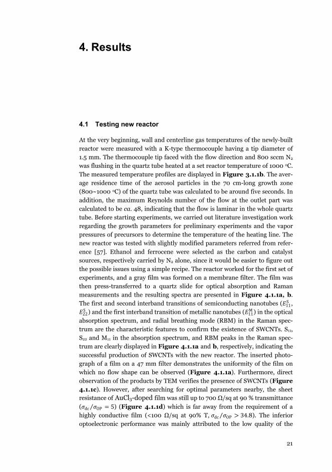
4.1 Testing new reactor
At the very beginning, wall and centerline gas temperatures of the newly-built reactor were measured with a K-type thermocouple having a tip diameter of 1.5 mm. The thermocouple tip faced with the flow direction and 800 sccm N2 was flushing in the quartz tube heated at a set reactor temperature of 1000 oC. The measured temperature profiles are displayed in Figure 3.1.1b. The aver-age residence time of the aerosol particles in the 70 cm-long growth zone (800~1000 oC) of the quartz tube was calculated to be around five seconds. In addition, the maximum Reynolds number of the flow at the outlet part was calculated to be ca. 48, indicating that the flow is laminar in the whole quartz tube. Before starting experiments, we carried out literature investigation work regarding the growth parameters for preliminary experiments and the vapor pressures of precursors to determine the temperature of the heating line. The new reactor was tested with slightly modified parameters referred from refer-ence [57]. Ethanol and ferrocene were selected as the carbon and catalyst sources, respectively carried by N2 alone, since it would be easier to figure out the possible issues using a simple recipe. The reactor worked for the first set of experiments, and a gray film was formed on a membrane filter. The film was then press-transferred to a quartz slide for optical absorption and Raman measurements and the resulting spectra are presented in Figure 4.1.1a, b. The first and second interband transitions of semiconducting nanotubes ( ,
) and the first interband transition of metallic nanotubes ( ) in the optical absorption spectrum, and radial breathing mode (RBM) in the Raman spec-trum are the characteristic features to confirm the existence of SWCNTs. S11, S22 and M11 in the absorption spectrum, and RBM peaks in the Raman spec-trum are clearly displayed in Figure 4.1.1a and b, respectively, indicating the successful production of SWCNTs with the new reactor. The inserted photo-graph of a film on a 47 mm filter demonstrates the uniformity of the film on which no flow shape can be observed (Figure 4.1.1a). Furthermore, direct observation of the products by TEM verifies the presence of SWCNTs (Figure 4.1.1c). However, after searching for optimal parameters nearby, the sheet resistance of AuCl3-doped film was still up to 700 Ω/sq at 90 % transmittance ( ) (Figure 4.1.1d) which is far away from the requirement of a highly conductive film (<100 Ω/sq at 90% T, 8). The inferior optoelectronic performance was mainly attributed to the low quality of the
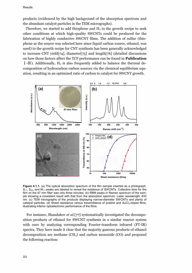
Results
22
products (evidenced by the high background of the absorption spectrum and the abundant catalyst particles in the TEM micrographs).
Therefore, we started to add thiophene and H2 to the growth recipe to seek other conditions at which high-quality SWCNTs could be produced for the fabrication of highly conductive SWCNT films. The addition of sulfur (thio-phene as the source was selected here since liquid carbon source, ethanol, was used) to the growth recipe for CNT synthesis has been generally acknowledged to increase CNT yield[74], diameter[75] and length[76] (detailed discussions on how those factors affect the TCF performance can be found in Publication
- ). Additionally, H2 is also frequently added to balance the thermal de-composition of hydrocarbon carbon sources via the chemical equilibrium equ-ation, resulting in an optimized ratio of carbon to catalyst for SWCNT growth.
Figure 4.1.1. (a) The optical absorption spectrum of the film sample inserted as a photograph. S11, S22, and M11 peaks are labeled to reveal the existence of SWCNTs. Collection time for the film on the 47 mm filter was only three minutes. (b) RBM peaks in Raman spectrum of the sam-ple showing a consistent result with that from the absorption spectrum. Laser wavelength: 633 nm. (c) TEM micrographs of the products displaying narrow-diameter SWCNTs and plenty of catalyst particles. (d) Sheet resistance versus transmittance of pristine and AuCl3-doped films, illustrating inferior optoelectronic performance of the films.
For instance, Shandakov et al.[77] systematically investigated the decompo-sition products of ethanol for SWCNT synthesis in a similar reactor system with ours by analyzing corresponding Fourier-transform infrared (FT-IR) spectra. They have made it clear that the majority gaseous products of ethanol decomposition are methane (CH4) and carbon monoxide (CO) and proposed the following reaction:
100 150 200 250 300 350
Inte
nsity
(a.u
.)
Raman shift (cm-1)
2.4 2 1.6 1.2 0.8dt (nm)
400 800 1200 1600 2000 2400
M11S11
Abs
orba
nce
(a.u
.)
Wavelength (nm)
S22
(a) (b)
(c)
47 mm filter
10 100 1000 10000
50
60
70
80
90
100 Pristine film AuCl3-doped
Tran
smitt
ance
at 5
50 n
m (%
)
Sheet resistance (Ω/sq)
(d)
Results
23
Apparently, the reaction was put forward based on stoichiometric chemistry according to the results analyzed from FT-IR spectra. There must exist some other decomposition routes to produce intermediates following the reactions which have been considered as the most important thermal decomposition means of ethanol at high temperatures[78]:
Then, CH4 and CO can be assumed to be produced via:
As a consequence, the concentration of H2 as one of the decomposed prod-ucts can shift the reaction 4.1.1 back and forward, and an appropriate volume of H2 is significant for the production of an optimal number of carbon atoms to grow high-quality SWCNTs.
4.2 Optimizing parameters after adding thiophene and H2
With the addition of thiophene and H2, the growth parameters were referred from reference [11] and optimized mainly by evaluating the optoelectronic per-formance, i.e., sheet resistance versus transmittance, of as-collected SWCNT films. Only those films collected at the optimal conditions were doped with AuCl3 to obtain lower sheet resistances. Compared with the commonly used dopant of nitric acid (HNO3), AuCl3 has been considered to be a more stable dopant which can downshift the Fermi level towards the valence band of SWCNTs, decreasing the Schottky barrier height and enhancing the film con-ductivity accordingly[79].
4.2.1 The effect of thiophene concentration
The starting feeding rate of the precursor solution was set to be 10 μl/min (the calculated vaporized gas flow rate is 3.8 sccm) in order to reduce the collection time. To study the sulfur effect, the concentration of thiophene was varied while that of ferrocene was fixed. According to the sheet resistance versus transmittance curves, the optimized ratio of sulfur to iron (S/Fe) is 0.2 (Fig-ure 4.2.1a). The sheet resistance of the pristine film collected at S/Fe=0.2 is around 487 Ω/sq at 90% T ( ). Analysis of the optical absorption spectra of the corresponding films with a transmittance close to 90% T indi-cates that the mean diameter of nanotubes increases with the increasing of

Results
24
S/Fe ratio, i.e., thiophene concentration. Furthermore, the S11 of the absorp-tion spectrum of the film collected with S/Fe=0.2 shifts to 2225 nm from 1160 nm when no thiophene was added (Figure 4.1.1a), corresponding to an in-crease in the mean diameter to 2.0 nm from 0.9 nm analyzed from the Kataura plot. Sulfur has been considered to decrease the carbon dissolution into cata-lyst by forming a 1~2 nm layer on the catalyst surface via Fe-S bonding, re-straining the supersaturation of carbon in catalyst particles and reducing the encapsulation of the particles by carbon coating (i.e., “poisoning” as claimed) accordingly[80–83]. At a low sulfur concentration, the superfluous decom-posed carbon radicals can still encapsulate some catalyst particles, leading to the presence of carbon-coated catalyst particles in the film[84]. However, the catalyst particles could be encapsulated by the sulfur layer if sulfur concentra-tion is too high, blocking enough carbon dissolution or surface diffusion for CNT growth[80,82]. Only an appropriate amount of sulfur enables the growth of high-quality SWCNTs. As for the increase in mean nanotube diameter with sulfur addition, several possible explanations have been proposed, e.g., surface diffusion of carbon atoms on the catalyst[80], the expansion of the active area on catalyst surface[85], an increased number of enlarged catalyst particles by the aggregation of active particles[81,82]. A further deeper investigation of the roes of sulfur in tuning the morphology and structure of SWCNTs is discussed in Chapter 4.4.
Figure 4.2.1. The effect of thiophene concentration. (a) Sheet resistance versus transmittance of pristine SWCNT films. The results are presented in Publication . Reproduced from Ref. [25] with permission from The Royal Society of Chemistry. (b) The optical absorption spectra of the corresponding films. S11 peak is labeled to indicate that mean nanotube diameter increases with S/Fe ratio. The feeding rate of precursor solution is 10 μl/min.
The background (comes from catalyst particles, amorphous carbon, and other carbonaceous products) area of the absorption spectrum has been calcu-lated to roughly estimate the purity of a CNT sample[34]. As seen from Figure 4.2.1b, the absorption spectrum with S/Fe=0.1 has the highest background which could support the interpretations and is responsible for the inferior TCF performance. Absorption alone is unable to provide enough information to illustrate the results shown in Figure 4.2.1a. Advanced characterizations like high-resolution TEM and elemental mapping of the catalyst particles (espe-
10 100 1000 1000050
60
70
80
90
100
S/Fe=0.1 S/Fe=0.2 S/Fe=0.25 S/Fe=0.3
Tran
sim
ittan
ce a
t 550
nm
(%)
Sheet resistance (Ω/sq)
(a) (b)
400 800 1200 1600 2000 2400
Abs
orba
nce
(a.u
.)
Wavelength (nm)
S/Fe=0.1 S/Fe=0.2 S/Fe=0.3
S11
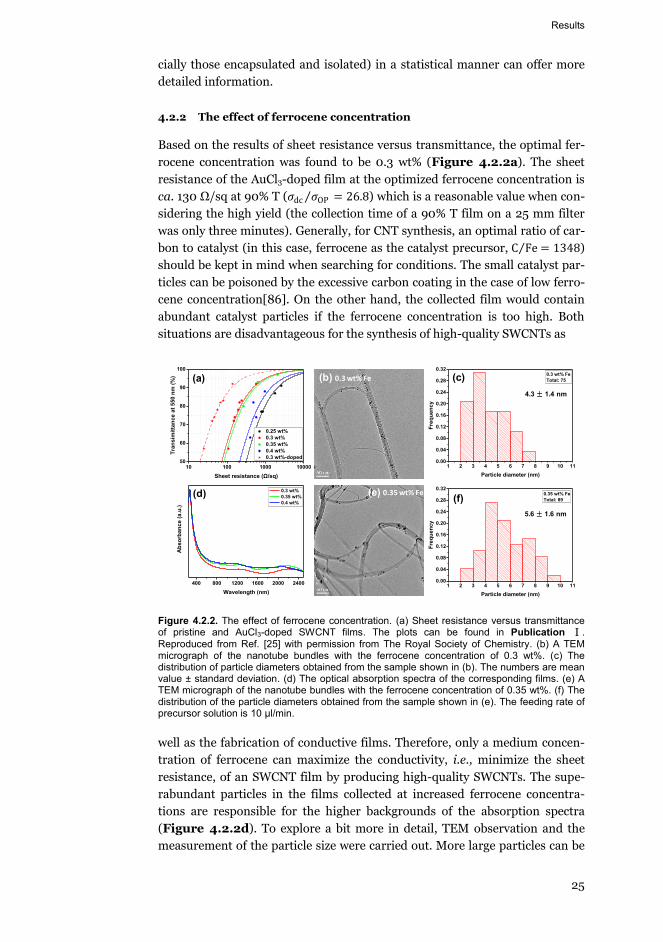
Results
25
cially those encapsulated and isolated) in a statistical manner can offer more detailed information.
4.2.2 The effect of ferrocene concentration
Based on the results of sheet resistance versus transmittance, the optimal fer-rocene concentration was found to be 0.3 wt% (Figure 4.2.2a). The sheet resistance of the AuCl3-doped film at the optimized ferrocene concentration is ca. 130 Ω/sq at 90% T ( ) which is a reasonable value when con-sidering the high yield (the collection time of a 90% T film on a 25 mm filter was only three minutes). Generally, for CNT synthesis, an optimal ratio of car-bon to catalyst (in this case, ferrocene as the catalyst precursor, ) should be kept in mind when searching for conditions. The small catalyst par-ticles can be poisoned by the excessive carbon coating in the case of low ferro-cene concentration[86]. On the other hand, the collected film would contain abundant catalyst particles if the ferrocene concentration is too high. Both situations are disadvantageous for the synthesis of high-quality SWCNTs as
Figure 4.2.2. The effect of ferrocene concentration. (a) Sheet resistance versus transmittance of pristine and AuCl3-doped SWCNT films. The plots can be found in Publication . Reproduced from Ref. [25] with permission from The Royal Society of Chemistry. (b) A TEM micrograph of the nanotube bundles with the ferrocene concentration of 0.3 wt%. (c) The distribution of particle diameters obtained from the sample shown in (b). The numbers are mean value ± standard deviation. (d) The optical absorption spectra of the corresponding films. (e) A TEM micrograph of the nanotube bundles with the ferrocene concentration of 0.35 wt%. (f) The distribution of the particle diameters obtained from the sample shown in (e). The feeding rate of precursor solution is 10 μl/min.
well as the fabrication of conductive films. Therefore, only a medium concen-tration of ferrocene can maximize the conductivity, i.e., minimize the sheet resistance, of an SWCNT film by producing high-quality SWCNTs. The supe-rabundant particles in the films collected at increased ferrocene concentra-tions are responsible for the higher backgrounds of the absorption spectra (Figure 4.2.2d). To explore a bit more in detail, TEM observation and the measurement of the particle size were carried out. More large particles can be
1 2 3 4 5 6 7 8 9 10 110.00
0.04
0.08
0.12
0.16
0.20
0.24
0.28
0.32
Freq
uenc
y
Particle diameter (nm)
0.3 wt% FeTotal: 75
1 2 3 4 5 6 7 8 9 10 110.00
0.04
0.08
0.12
0.16
0.20
0.24
0.28
0.32
Freq
uenc
y
Particle diameter (nm)
0.35 wt% FeTotal: 89
10 100 1000 1000050
60
70
80
90
100
0.25 wt% 0.3 wt% 0.35 wt% 0.4 wt% 0.3 wt%-doped
Tran
sim
ittan
ce a
t 550
nm
(%)
Sheet resistance (Ω/sq)
(a) (b) (c)
(d) (e) (f)
0.3 wt% Fe
0.35 wt% Fe
400 800 1200 1600 2000 2400
Abs
orba
nce
(a.u
.)
Wavelength (nm)
0.3 wt% 0.35 wt% 0.4 wt%
4.3 1.4 nm
5.6 1.6 nm
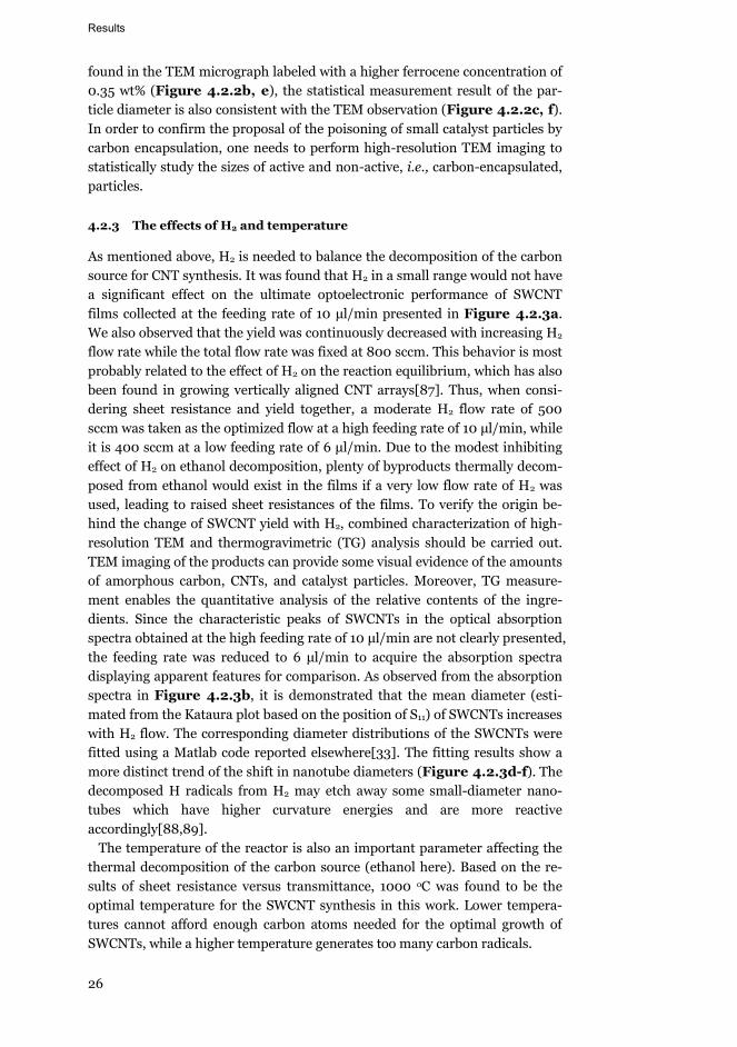
Results
26
found in the TEM micrograph labeled with a higher ferrocene concentration of 0.35 wt% (Figure 4.2.2b, e), the statistical measurement result of the par-ticle diameter is also consistent with the TEM observation (Figure 4.2.2c, f). In order to confirm the proposal of the poisoning of small catalyst particles by carbon encapsulation, one needs to perform high-resolution TEM imaging to statistically study the sizes of active and non-active, i.e., carbon-encapsulated, particles.
4.2.3 The effects of H2 and temperature
As mentioned above, H2 is needed to balance the decomposition of the carbon source for CNT synthesis. It was found that H2 in a small range would not have a significant effect on the ultimate optoelectronic performance of SWCNT films collected at the feeding rate of 10 μl/min presented in Figure 4.2.3a. We also observed that the yield was continuously decreased with increasing H2 flow rate while the total flow rate was fixed at 800 sccm. This behavior is most probably related to the effect of H2 on the reaction equilibrium, which has also been found in growing vertically aligned CNT arrays[87]. Thus, when consi-dering sheet resistance and yield together, a moderate H2 flow rate of 500 sccm was taken as the optimized flow at a high feeding rate of 10 μl/min, while it is 400 sccm at a low feeding rate of 6 μl/min. Due to the modest inhibiting effect of H2 on ethanol decomposition, plenty of byproducts thermally decom-posed from ethanol would exist in the films if a very low flow rate of H2 was used, leading to raised sheet resistances of the films. To verify the origin be-hind the change of SWCNT yield with H2, combined characterization of high-resolution TEM and thermogravimetric (TG) analysis should be carried out. TEM imaging of the products can provide some visual evidence of the amounts of amorphous carbon, CNTs, and catalyst particles. Moreover, TG measure-ment enables the quantitative analysis of the relative contents of the ingre-dients. Since the characteristic peaks of SWCNTs in the optical absorption spectra obtained at the high feeding rate of 10 μl/min are not clearly presented, the feeding rate was reduced to 6 μl/min to acquire the absorption spectra displaying apparent features for comparison. As observed from the absorption spectra in Figure 4.2.3b, it is demonstrated that the mean diameter (esti-mated from the Kataura plot based on the position of S11) of SWCNTs increases with H2 flow. The corresponding diameter distributions of the SWCNTs were fitted using a Matlab code reported elsewhere[33]. The fitting results show a more distinct trend of the shift in nanotube diameters (Figure 4.2.3d-f). The decomposed H radicals from H2 may etch away some small-diameter nano-tubes which have higher curvature energies and are more reactive accordingly[88,89].
The temperature of the reactor is also an important parameter affecting the thermal decomposition of the carbon source (ethanol here). Based on the re-sults of sheet resistance versus transmittance, 1000 oC was found to be the optimal temperature for the SWCNT synthesis in this work. Lower tempera-tures cannot afford enough carbon atoms needed for the optimal growth of SWCNTs, while a higher temperature generates too many carbon radicals.
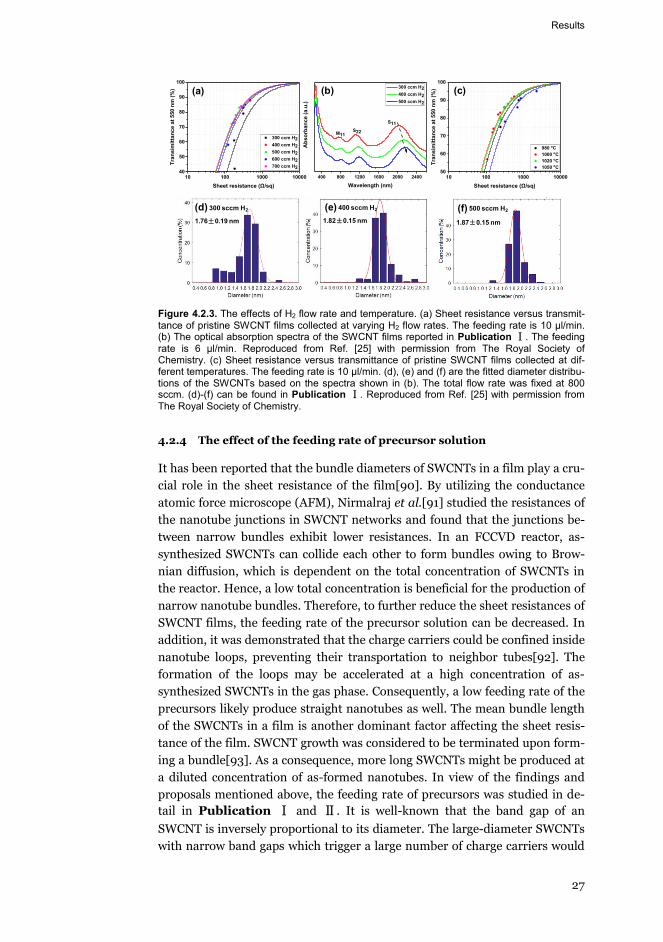
Results
27
Figure 4.2.3. The effects of H2 flow rate and temperature. (a) Sheet resistance versus transmit-tance of pristine SWCNT films collected at varying H2 flow rates. The feeding rate is 10 μl/min. (b) The optical absorption spectra of the SWCNT films reported in Publication . The feeding rate is 6 μl/min. Reproduced from Ref. [25] with permission from The Royal Society of Chemistry. (c) Sheet resistance versus transmittance of pristine SWCNT films collected at dif-ferent temperatures. The feeding rate is 10 μl/min. (d), (e) and (f) are the fitted diameter distribu-tions of the SWCNTs based on the spectra shown in (b). The total flow rate was fixed at 800 sccm. (d)-(f) can be found in Publication . Reproduced from Ref. [25] with permission from The Royal Society of Chemistry.
4.2.4 The effect of the feeding rate of precursor solution
It has been reported that the bundle diameters of SWCNTs in a film play a cru-cial role in the sheet resistance of the film[90]. By utilizing the conductance atomic force microscope (AFM), Nirmalraj et al.[91] studied the resistances of the nanotube junctions in SWCNT networks and found that the junctions be-tween narrow bundles exhibit lower resistances. In an FCCVD reactor, as-synthesized SWCNTs can collide each other to form bundles owing to Brow-nian diffusion, which is dependent on the total concentration of SWCNTs in the reactor. Hence, a low total concentration is beneficial for the production of narrow nanotube bundles. Therefore, to further reduce the sheet resistances of SWCNT films, the feeding rate of the precursor solution can be decreased. In addition, it was demonstrated that the charge carriers could be confined inside nanotube loops, preventing their transportation to neighbor tubes[92]. The formation of the loops may be accelerated at a high concentration of as-synthesized SWCNTs in the gas phase. Consequently, a low feeding rate of the precursors likely produce straight nanotubes as well. The mean bundle length of the SWCNTs in a film is another dominant factor affecting the sheet resis-tance of the film. SWCNT growth was considered to be terminated upon form-ing a bundle[93]. As a consequence, more long SWCNTs might be produced at a diluted concentration of as-formed nanotubes. In view of the findings and proposals mentioned above, the feeding rate of precursors was studied in de-tail in Publication and . It is well-known that the band gap of an SWCNT is inversely proportional to its diameter. The large-diameter SWCNTs with narrow band gaps which trigger a large number of charge carriers would
10 100 1000 1000040
50
60
70
80
90
100
300 ccm H2 400 ccm H2 500 ccm H2 600 ccm H2 700 ccm H2
Tran
sim
ittan
ce a
t 550
nm
(%)
Sheet resistance (Ω/sq)10 100 1000 10000
50
60
70
80
90
100
980 oC 1000 oC 1020 oC 1050 oC
Tran
sim
ittan
ce a
t 550
nm
(%)
Sheet resistance (Ω/sq)400 800 1200 1600 2000 2400
M11S22
Abs
orba
nce
(a.u
.)
Wavelength (nm)
300 ccm H2 400 ccm H2 500 ccm H2
S11
1.76 0.19 nm 1.82 0.15 nm 1.87 0.15 nm
(a) (c)
(f)(e)(d)
(b)
300 sccm H2 400 sccm H2 500 sccm H2

Results
28
be favorable for the fabrication of SWCNT TCFs. As a result, an SWCNT film comprising narrow, straight and long bundles as well as large-diameter SWCNTs should be preferable for their application in the conductive films. Here, we have been trying to optimize the growth parameters to reach those targets in the studies presented in this dissertation.
Figure 4.2.4. (a), (b) and (c) are TEM micrographs of the SWCNT bundles synthesized at the feeding rates of 8 μl/min, 6 μl/min and 4 μl/min, respectively. (a) and (c) were displayed in Pub-lication , (b) in Publication . Reproduced from Refs. [68] and [25], respectively with permissions from The Royal Society of Chemistry. (d), (e) and (f) are the histogram distributions of the bundle diameters in the samples represented by (a), (b) and (c), respectively.
TEM was employed to check the morphologies of the SWCNT bundles. Sev-eral individual SWCNTs and narrow bundles consisting of two or three SWCNTs are displayed in the TEM micrograph of the SWCNT sample col-lected at the feeding rate of 4 μl/min (Figure 4.2.4c), while only large bun-dles are visible in the samples collected at higher feeding rates (Figure 4.2.4a, b). A statistical measurement of the nanotube bundles in the three samples shows that the mean bundle diameter of SWCNTs synthesized at the feeding rates of 8 μl/min, 6 μl/min, and 4 μl/min are 10.2 nm, 6.3 nm, and 5.3 nm, respectively (Figure 4.2.4d-f). Among them, the individual SWCNTs account for 24.6% in the sample collected at the lowest feeding rate. The diameter dis-tribution of the extracted individual SWCNTs (totally 62 tubes, can be found in Publication ) demonstrates that the mean diameter of the SWCNTs is 2.1 nm. The decreased bundle diameter and increased percentage of individual SWCNTs are ascribed to the low feeding rate which leads to a reduced total concentration of catalyst particles and carbon radicals for nanotube growth. As a consequence, as-synthesized SWCNTs in the gas phase have fewer chances to collide each other, giving rise to the formation of narrow bundles and a grow-ing percentage of isolated SWCNTs. The number of conduction paths for the charge carriers in narrow bundles or even individual SWCNTs is much higher than that in large bundles, as charge carriers mainly transport at the bundle surface and that inboard nanotubes only contribute to optical absorption[90].
0 2 4 6 8 10 12 14 16 18 20 22 240.00
0.04
0.08
0.12
0.16
0.20
0.24
0.28
0.32
Freq
uenc
y
Bundle diameter (nm)
Total: 252
5.3 3.0nm
(c)
(f)
(a)
0 4 8 12 16 20 24 28 32 360.00
0.04
0.08
0.12
0.16
0.20
Freq
uenc
y
Bundle diameter (nm)
Total: 182(d)10.2 5.4 nm
20 nm20 nm
8 μl/min
8 μl/min
0 2 4 6 8 10 12 14 16 18 20 220.00
0.04
0.08
0.12
0.16
0.20
0.24
0.28
0.32
Freq
uenc
y
Bundle diameter (nm)
Total: 144 4 μl/min(e) 6 μl/min6.3 3.8nm
4 μl/min
20 nm
(b) 6 μl/min
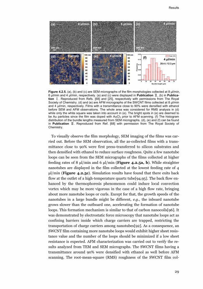
Results
29
Figure 4.2.5. (a), (b) and (c) are SEM micrographs of the film morphologies collected at 8 μl/min, 6 μl/min and 4 μl/min, respectively. (a) and (c) were displayed in Publication , (b) in Publica-tion . Reproduced from Refs. [68] and [25], respectively with permissions from The Royal Society of Chemistry. (d) and (e) are AFM micrographs of the SWCNT films collected at 8 μl/min and 4 μl/min, respectively. Films with a transmittance close to 90% were densified with ethanol before SEM and AFM observations. The whole area was considered for RMS analysis in (d) while only the white square was taken into account in (e). The bright spots in (e) are deemed to be Au particles since the film was doped with AuCl3 prior to AFM scanning. (f) The histogram distribution of the bundle lengths measured from SEM micrographs. (d), (e) and (f) can be found in Publication . Reproduced from Ref. [68] with permission from The Royal Society of Chemistry.
To visually observe the film morphology, SEM imaging of the films was car-ried out. Before the SEM observation, all the as-collected films with a trans-mittance close to 90% were first press-transferred to silicon substrates and then densified with ethanol to reduce surface roughness. Quite a few nanotube loops can be seen from the SEM micrographs of the films collected at higher feeding rates of 8 μl/min and 6 μl/min (Figure 4.2.5a, b). While straighter nanotubes are displayed in the film collected at the lowest feeding rate of 4 μl/min (Figure 4.2.5c). Simulation results have found that there exits back flow at the outlet of a high-temperature quartz tube[94,95]. The back flow en-hanced by the thermophoresis phenomenon could induce local convection vortex which may be more vigorous in the case of a high flow rate, bringing about more nanotube loops or curls. Except for that, the growth speeds of the nanotubes in a large bundle might be different, e.g., the inboard nanotube grows slower than the outboard one, accelerating the formation of nanotube loops. This formation mechanism is similar to that of carbon nanocoils[96]. It was demonstrated by electrostatic force microscopy that nanotube loops act as confining barriers inside which charge carriers are trapped, restricting the transportation of charge carriers among nanotubes[92]. As a consequence, an SWCNT film containing more nanotube loops would exhibit higher sheet resis-tance value and the number of the loops should be minimized if a low sheet resistance is expected. AFM characterization was carried out to verify the re-sults analyzed from TEM and SEM micrographs. The SWCNT films having a transmittance around 90% were densified with ethanol as well before AFM scanning. The root-mean-square (RMS) roughness of the SWCNT film col-
0 10 20 30 40 50 60 700.00
0.04
0.08
0.12
0.16
0.20
Freq
uenc
y
Bundle length (μm)
Total: 274
400 nm
28.4 12.3 μm
(a) (c)
(f)(e)
400 nm
8 μl/min
(d) 8 μl/min
400 nm
(b) 6 μl/min 4 μl/min
4 μl/min4 μl/min
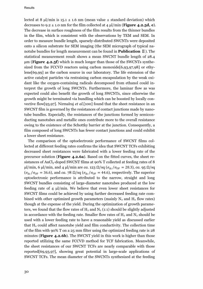
Results
30
lected at 8 μl/min is 15.1 ± 1.6 nm (mean value ± standard deviation) which decreases to 9.2 ± 1.0 nm for the film collected at 4 μl/min (Figure 4.2.5d, e). The decrease in surface roughness of the film results from the thinner bundles in the film, which is consistent with the observations by TEM and SEM. In order to measure bundle length, sparsely-distributed SWCNTs were deposited onto a silicon substrate for SEM imaging (the SEM micrograph of typical na-notube bundles for length measurement can be found in Publication ). The statistical measurement result shows a mean SWCNT bundle length of 28.4 μm (Figure 4.2.5f) which is much longer than those of the SWCNTs synthe-sized from the FCCVD reactors using carbon monoxide[6,93,97,98] or ethy-lene[69,99] as the carbon source in our laboratory. The life extension of the active catalyst particles via restraining carbon encapsulation by the weak oxi-dant like the oxygen-containing radicals decomposed from ethanol could in-terpret the growth of long SWCNTs. Furthermore, the laminar flow as was expected could also benefit the growth of long SWCNTs, since otherwise the growth might be terminated via bundling which can be boosted by locally con-vective flow[93,97]. Nirmalraj et al.[100] found that the sheet resistance in an SWCNT film is governed by the resistances of contact junctions made by nano-tube bundles. Especially, the resistances of the junctions formed by semicon-ducting nanotubes and metallic ones contribute more to the overall resistance owing to the existence of the Schottky barrier at the junction. Consequently, a film composed of long SWCNTs has fewer contact junctions and could exhibit a lower sheet resistance.
The comparison of the optoelectronic performance of SWCNT films col-lected at different feeding rates confirms the idea that SWCNT TCFs exhibiting decreased sheet resistances were fabricated with a lower feeding rate of the precursor solution (Figure 4.2.6a). Based on the fitted curves, the sheet re-sistances of AuCl3-doped SWCNT films at 90% T collected at feeding rates of 8 μl/min, 6 μl/min, and 4 μl/min are ca. 123 Ω/sq ( ), ca. 95 Ω/sq ( ), and ca. 78 Ω/sq ( ), respectively. The superior optoelectronic performance is attributed to the narrow, straight and long SWCNT bundles consisting of large-diameter nanotubes produced at the low feeding rate of 4 μl/min. We believe that even lower sheet resistances for SWCNT films could be achieved by using further decreased feeding rate com-bined with other optimized growth parameters (mainly N2 and H2 flow rates) though at the expense of the yield. During the optimization of growth parame-ters, we found that the flow rates of H2 and N2 (1:1) should be slightly adjusted in accordance with the feeding rate. Smaller flow rates of H2 and N2 should be used with a lower feeding rate to have a reasonable yield as discussed earlier that H2 could affect nanotube yield and film conductivity. The collection time of the film with 90% T on a 25 mm filter using the optimized feeding rate is 28 minutes (Figure 4.2.6b). The SWCNT yield in this work is higher than those reported utilizing the same FCCVD method for TCF fabrication. Meanwhile, the sheet resistances of our SWCNT TCFs are nearly comparable with those reported[69,93,97], showing great potential in large-scale applications of SWCNT TCFs. The mean diameter of the SWCNTs synthesized at the feeding
Results
31
rate of 4 μl/min is around 2 nm, and more than 60% of the SWCNTs have di-ameters in the range of 1.8~2.2 nm (obtained with the Matlab fitting, and re-ported in Publication ). The diameters calculated from the absorption spectrum match those obtained from the TEM micrographs. As mentioned above, the large-diameter SWCNTs are one of the contributors to the lowest sheet resistance achieved at 4 μl/min. The disappearance of van Hove singu-larity transition peaks S11 and S22 in the absorption spectrum of AuCl3-doped SWCNT film is ascribed to the increased work function of SWCNTs and a downshift in the Fermi level towards the valence band, which is induced by the charge transfer from SWCNTs to AuCl3[79].
Figure 4.2.6. (a) Sheet resistance versus transmittance curves of pristine and doped SWCNT films collected at different feeding rates. (b) Collection time versus transmittance. A filter with a diameter of 25 mm was used for film collection. (c) The optical absorption spectra of the SWCNT films. The film collected at the feeding rate of 4 μl/min was doped with AuCl3 to demon-strate the doping effect. (d) and (e) are the RBM peaks in Raman spectra excited by 488 nm and 633 nm laser, respectively. (f) G and D bands in Raman spectra of the SWCNT films. Laser wavelength is 633 nm. All the data were re-plotted based on the original data reported in Publi-cation and . Adapted from Refs. [25] and [68], respectively with permissions from The Royal Society of Chemistry.
Raman spectroscopy characterization is a semi-quantitative method to esti-mate the quality of SWCNTs by calculating the ratio of either intensities or integrated areas of G and D bands. As seen from the Raman spectra shown in Figure 4.2.6f, the D bands are almost invisible, revealing the excellent quali-ty of the SWCNT films. The intensity ratio of G and D bands, IG/ID, in the Ra-man spectra of the films at feeding rates of 8 μl/min, 6 μl/min, and 4 μl/min are 95, 125, and 106, respectively (details and the Raman spectra exited using other lasers can be found in Publication and ). The positions of RBM peaks in a Raman spectrum can be utilized to calculate the diameters of SWCNTs following formula 2.3.1. The calculated diameters of resonant SWCNTs are consistent with the results analyzed from the corresponding ab-sorption spectra. Additionally, more large-diameter SWCNTs can be found using the optimal feeding rate of 4 μl/min based on the analysis from RBM peaks (Figure 4.2.6d, e).
50 100 150 200 250 300
Inte
nsity
(a.u
.)
Raman shift (cm-1)
8 μl-400 H2 6 μl-400 H2 4 μl-300 H2
488 nm
50 100 150 200 250 300
633 nm
Inte
nsity
(a.u
.)
Raman shift (cm-1)
8 μl-400 H2 6 μl-400 H2 4 μl-300 H2
1200 1300 1400 1500 1600 1700 1800
D
633 nm
Inte
nsity
(a.u
.)
Raman shift (cm-1)
8 μl-400 H2 6 μl-400 H2 4 μl-300 H2
G
400 800 1200 1600 2000 2400 2800
M11S22
Abs
orba
nce
(a.u
.)
Wavelength (nm)
8 μl-400 H2-pristine 4 μl-300 H2-pristine 4 μl-300 H2-doped
S11
0 10 20 30 40 50 6050
60
70
80
90
100
6 μl-400 H2 4 μl-300 H2
Tran
smitt
ance
at 5
50 n
m (%
)
Collection time (min)
25 mm filter
10 100 1000 1000050
60
70
80
90
100
8 μl-400 H2-pristine 6 μl-400 H2-pristine 4 μl-300 H2-pristine 8 μl-400 H2-doped 6 μl-400 H2-doped 4 μl-300 H2-dopedTr
ansi
mitt
ance
at 5
50 n
m (%
)
Sheet resistance (Ω/sq)
(a) (c)
(f)(e)(d)
(b)
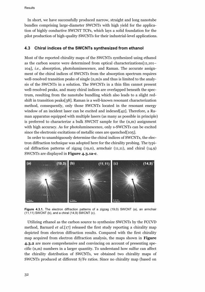
Results
32
In short, we have successfully produced narrow, straight and long nanotube bundles comprising large-diameter SWCNTs with high yield for the applica-tion of highly conductive SWCNT TCFs, which lays a solid foundation for the pilot production of high-quality SWCNTs for their industrial-level applications.
4.3 Chiral indices of the SWCNTs synthesized from ethanol
Most of the reported chirality maps of the SWCNTs synthesized using ethanol as the carbon source were determined from optical characterizations[11,101–104], i.e., absorption, photoluminescence, and Raman. The accurate assign-ment of the chiral indices of SWCNTs from the absorption spectrum requires well-resolved transition peaks of single (n,m)s and thus is limited to the analy-sis of the SWCNTs in a solution. The SWCNTs in a thin film cannot present well-resolved peaks, and many chiral indices are overlapped beneath the spec-trum, resulting from the nanotube bundling which also leads to a slight red-shift in transition peaks[38]. Raman is a well-known resonant characterization method, consequently, only those SWCNTs located in the resonant energy window of an incident laser can be excited and indexed[42]. Therefore, a Ra-man apparatus equipped with multiple lasers (as many as possible in principle) is preferred to characterize a bulk SWCNT sample for the (n,m) assignment with high accuracy. As for photoluminescence, only s-SWCNTs can be excited since the electronic excitations of metallic ones are quenched[105].
In order to unambiguously determine the chiral indices of SWCNTs, the elec-tron diffraction technique was adopted here for the chirality probing. The typi-cal diffraction patterns of zigzag (19,0), armchair (11,11), and chiral (14,9) SWCNTs are displayed in Figure 4.3.1a-c.
Figure 4.3.1. The electron diffraction patterns of a zigzag (19,0) SWCNT (a), an armchair(11,11) SWCNT (b), and a chiral (14,9) SWCNT (c).
Utilizing ethanol as the carbon source to synthesize SWCNTs by the FCCVD method, Barnard et al.[17] released the first study reporting a chirality map depicted from electron diffraction results. Compared with the first chirality map acquired from electron diffraction analysis, the maps shown in Figure 4.3.2 are more comprehensive and convincing on account of presenting spe-cific (n,m) numbers in a larger quantity. To understand how sulfur can affect the chirality distribution of SWCNTs, we obtained two chirality maps of SWCNTs produced at different S/Fe ratios. Since no chirality map (based on
Results
33
electron diffraction analysis) regarding the sulfur effect on ethanol-synthesized SWCNTs by FCCVD can be found ahead of the moment of writing the disserta-tion, the results presented here are much meaningful and can examine the maps depicted from the optical characterization results. At first glance, no ob-vious difference in the distributions of (n,m) can be found based on the maps displayed in Figure 4.3.2a and b. The majority of SWCNTs are near-armchair tubes, while some tubes are close to zigzag type. Some large-diameter SWCNTs are scattered beyond 2 nm since there exist more chiral indices in the large-diameter region. The analysis is also supported by the di-ameter and chiral angle distributions (Figure 4.3.2e, f, h and i). The optical absorption spectra of the SWCNTs for diffraction are displayed in Figure 4.3.2c. The absorption spectra indicate a modest increase in the mean diame-ter of SWCNTs with raising the sulfur concentration. Almost all the previous studies regarding the sulfur effect on SWCNT growth have confirmed that the addition of sulfur leads to an increase in the mean diameter of SWCNTs and a shift in chiral indices to the large-diameter region in a chirality map. However, as seen from the results studied here, a slight change of sulfur concentration in the growth recipe does not make a noticeable influence on the chirality distri-bution of SWCNTs. We have also carried out the research regarding the sulfur (sulfur source is H2S) effect on the chirality distribution of SWCNTs produced by a spark-discharge reactor, concluding that sulfur has little influence on the chirality modulating of SWCNTs[106]. It is supposed that a more distinct vari-ation of sulfur concentration would result in an apparent shift in chiral indices. Therefore, to probe the role of sulfur in shifting SWCNT chiralities, the chirali-ty maps obtained with and without sulfur (while all other growth parameters are kept constant) should be compared, though the quality of SWCNTs in both cases cannot be ensured to be high enough for gathering a statistically reliable number of electron diffraction patterns. For instance, there are some reports where no CNTs were found without adding thiophene to the growth recipe[107], or only a few short CNTs were observed with the absence of sul-fur[76].
In addition to the sulfur effect, the effect of H2 on the chirality distribution of SWCNTs was investigated as well. There is no apparent shift in chiral indic-es either when comparing the chirality maps displayed in Figure 4.3.2b and d. The mean diameter and diameter distributions of SWCNTs almost coincide with those analyzed from the absorption spectra shown in Figure 4.2.3b. Gathering more electron diffraction patters would minimize the slight discre-pancy. In all, based on the diffraction results, the mean diameters of SWCNTs in all the three cases locate in the range of 1.7~1.8 nm, and the mean chiral angles around 20o. It is worthy to mention that the purity of s-SWCNTs in all the cases ranges from 75% to 77%. As a whole, the chirality distributions pre-sented in these cases are consistent with those reported previously using etha-nol as the carbon source for SWCNT synthesis[17,108,109], indicating that the optical characterization techniques can be employed for a rough estimation of the SWCNT chiralities to enable timely feedback to the growth parameters.
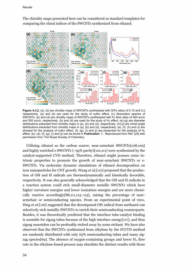
Results
34
The chirality maps presented here can be considered as standard templates for comparing the chiral indices of the SWCNTs synthesized from ethanol.
Figure 4.3.2. (a), (b) are chirality maps of SWCNTs synthesized with S/Fe ratios of 0.15 and 0.2, respectively. (a) and (b) are used for the study of sulfur effect. (c) Absorption spectra of SWCNTs. (b) and (d) are chirality maps of SWCNTs synthesized with H2 flow rates of 400 sccm and 500 sccm, respectively. (b) and (d) are used for the study of H2 effect. (e)-(g) are diameter distributions extracted from chirality maps in (a), (b) and (d), respectively. (h)-(j) are chiral angle distributions extracted from chirality maps in (a), (b) and (d), respectively. (e), (f), (h) and (i) are showed for the analysis of sulfur effect. (f), (g), (i) and (j) are presented for the analysis of H2 effect. (b), (d), (f), (g), (i) and (j) can be found in Publication . Reproduced from Ref. [25] with permission from The Royal Society of Chemistry.
Utilizing ethanol as the carbon source, near-armchair SWCNTs[108,109] and highly enriched s-SWCNTs (~95% purity)[110,111] were synthesized by the catalyst-supported CVD method. Therefore, ethanol might possess some in-trinsic properties to promote the growth of near-armchair SWCNTs or s-SWCNTs. Via molecular dynamic simulations of ethanol decomposition on iron nanoparticles for CNT growth, Wang et al.[112] proposed that the produc-tion of OH and H radicals are thermodynamically and kinetically favorable, respectively. It was also generally acknowledged that the OH and H radicals in a reaction system could etch small-diameter metallic SWCNTs which have higher curvature energies and lower ionization energies and are more chemi-cally reactive accordingly[88,111,113–115], raising the percentage of near-armchair or semiconducting species. From an experimental point of view, Ding et al.[116] suggested that the decomposed OH radical from methanol can selectively etch metallic SWCNTs to enrich their semiconducting counterparts. Besides, it was theoretically predicted that the interface tube-catalyst binding is unstable for zigzag tubes because of the high interface energy[117], and thus zigzag nanotubes can be preferably etched away by some etchant. We have also observed that the SWCNTs synthesized from ethylene by the FCCVD method are randomly distributed with only 65% semiconducting tubes and many zig-zag species[69]. The absence of oxygen-containing groups and lower H2 flow rate in the ethylene-based process may elucidate the distinct results with those
Total: 168 tubess-SWCNT purity : 76.8%
Total: 178 tubess-SWCNT purity : 75.3%
Total: 178 tubess-SWCNT purity: 76.4%
(d)
(a)2 nm
1.2 1.6 2.0 2.4 2.80.00
0.10
0.20
0.30
0.40
SWCNT diameter (nm)
S0.2-400 H2Total: 168 tubes
0 5 10 15 20 25 300.00
0.05
0.10
0.15
Chiral angle (o)
S0.2-400 H2Total: 168 tubes
1.2 1.6 2.0 2.4 2.80.00
0.10
0.20
0.30
0.40
SWCNT diameter (nm)
S0.2-500 H2Total:178 tubes
0 5 10 15 20 25 300.00
0.05
0.10
0.15
Chiral angle (o)
S0.2-500 H2Total: 178 tubes
1.2 1.6 2.0 2.4 2.80.00
0.10
0.20
0.30
0.40
0.50
Freq
uenc
y
SWCNT diameter (nm)
S0.15-400 H2Total: 178 tubes
0 5 10 15 20 25 300.00
0.05
0.10
0.15
Freq
uenc
y
Chiral angle (o)
S0.15-400 H2Total: 178 tubes
2 nm
(b)
(e) (f) (g)
(h) (i) (j)
400 800 1200 1600 2000 2400
Abs
orba
nce
(a.u
.)
Wavelength (nm)
S/Fe=0.15 S/Fe=0.2
S11
(c)
1.72 0.26 nm 1.67 0.22 nm 1.80 0.27 nm
20.2 7.8 (o) 19.4 8.0 (o) 18.9 8.0 (o)
Results
35
presented here. However, more solid evidence, e.g., the chirality maps ac-quired from the SWCNTs synthesized using a mixture of ethanol and methanol (or water) as the feedstock together with the investigation of the lattice struc-ture of the catalyst particle are needed to confirm the statements. Additionally, it is also possible that the oxygen-containing radicals could modify the struc-ture and/or morphology of catalyst nanoparticles, bringing about the appear-ance of a specific lattice plane for the selective growth of near-armchair tubes or s-SWCNTs. The modification of catalyst by the radicals has been confirmed by TEM observation of the catalyst nanoparticles[118]. In-situ TEM tracking of the evolution process of catalyst nanoparticles could verify the possible mod-ification of catalyst by some radicals[119].
4.4 Independent study on the roles of sulfur
As mentioned in Chapter 4.2.1, the effect of sulfur on SWCNT synthesis should be studied systematically. Here, by using a spark-discharge FCCVD reactor, we independently investigated the roles of sulfur (H2S as the sulfur source) in growing SWCNTs for the fabrication of TCFs. The effect of sulfur on the yield, diameter, quality, and length of SWCNTs as well as the optoelectronic perfor-mance of SWCNT TCFs was studied in detail.
The SWCNT yield was found to be sensitive to the sulfur concentration. The yield first increases then decreases with increasing the H2S concentration in the reactor (Figure 4.4.1a). The addition of an optimal amount of H2S leads to a 2.5-fold increase in the SWCNT yield. The effect of sulfur on the SWCNT growth was also found to be catalyst-dependent since the optimal sulfur con-centration which was required to achieve the maximum yield was different for Fe and Co catalysts. The regulation of CNT yield by sulfur has been reported in many cases[74,76,107,120]. Another generally acknowledged role of sulfur is to increase the CNT diameter[81,107,121], which has been also confirmed in our work. The S11 peak in the optical absorption spectra obtained with sulfur addi-tion behaves a redshift of ca. 200 nm (Figure 4.4.1b), indicating the increase in the mean diameter of SWCNTs. For instance, the mean diameter of the SWCNTs synthesized from Fe as the catalyst increases to 1.26 nm from 1.06 nm owing to the addition of 5 ppm H2S (Figure 4.4.1d). Besides, the IG/ID ratio in Raman spectra of the SWCNTs rises with the addition of an appropri-ate amount of sulfur (Figure 4.4.1c), implying the improvement of SWCNT quality.
To explore how sulfur can change SWCNT yield and diameter, TEM, energy-dispersive X-ray spectroscopy (EDS), and X-ray photoelectron spectroscopy (XPS) characterizations were performed. The TEM observation and EDS anal-ysis demonstrated that there is no obvious change in either the size or the composition of the catalyst particles with the addition of H2S. In contrast, the XPS analysis of the SWCNTs indicated the presence of both Fe (0.04 at%) and S (0.05 at%) (see Figure S6 in Publication ). The two peaks located 707 eV and 720 eV were displayed in the Fe 2p spectrum, manifesting the existence of metallic Fe. As for S, there exist two broad S 2p features between 161~166
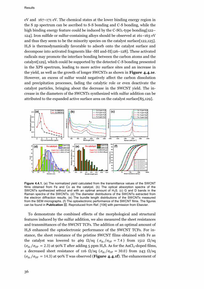
Results
36
eV and 167~171 eV. The chemical states at the lower binding energy region in the S 2p spectrum can be ascribed to S-S bonding and C-S bonding, while the high binding energy feature could be induced by the C-SOx-type bonding[122–124]. Iron sulfide or sulfur-containing alloys should be observed at 161~163 eV and thus they seem to be the minority species on the catalyst surface[122,125]. H2S is thermodynamically favorable to adsorb onto the catalyst surface and decompose into activated fragments like -SH and-H[126–128]. These activated radicals may promote the interface bonding between the carbon atoms and the catalyst[129], which could be supported by the detected C-S bonding presented in the XPS spectrum, leading to more active surface sites and an increase in the yield, as well as the growth of longer SWCNTs as shown in Figure 4.4.1e. However, an excess of sulfur would negatively affect the carbon dissolution and precipitation processes, fading the catalytic role or even deactivate the catalyst particles, bringing about the decrease in the SWCNT yield. The in-crease in the diameters of the SWCNTs synthesized with sulfur addition can be attributed to the expanded active surface area on the catalyst surface[85,129].
Figure 4.4.1. (a) The normalized yield calculated from the transmittance values of the SWCNT films obtained from Fe and Co as the catalyst. (b) The optical absorption spectra of the SWCNTs synthesized without and with an optimal amount of H2S. (c) G and D bands in the Raman spectra of the SWCNTs. (d) The diameter distributions of the SWCNTs extracted from the electron diffraction results. (e) The bundle length distributions of the SWCNTs measured from the SEM micrographs. (f) The optoelectronic performance of the SWCNT films. The figures can be found in Publication . Reproduced from Ref. [106] with permission from Elsevier.
To demonstrate the combined effects of the morphological and structural features induced by the sulfur addition, we also measured the sheet resistances and transmittances of the SWCNT TCFs. The addition of an optimal amount of H2S enhanced the optoelectronic performance of the SWCNT TCFs. For in-stance, the sheet resistance of the pristine SWCNT films obtained with Fe as the catalyst was lowered to 469 Ω/sq ( ) from 1512 Ω/sq ( ) at 90% T after adding 5 ppm H2S. As for the AuCl3-doped films, a decreased sheet resistance of 116 Ω/sq ( ) from 243 Ω/sq ( ) at 90% T was observed (Figure 4.4.1f). The enhancement of
0 2 4 6 8 100.0
0.5
1.0
1.5
2.0
2.5 Fe-SWCNTs Co-SWCNTs
H2S concentration (ppm)
Nor
mal
ized
yie
ld (a
.u.)
400 800 1200 1600 2000 2400
Co 8 ppm H2S Fe 5 ppm H2S Co 0 ppm H2S Fe 0 ppm H2S
Wavlength (nm)
Inte
nsity
(a.u
.)
0.6 0.8 1.0 1.2 1.4 1.6 1.8 2.00
5
10
15
20
25
30
35
Cou
nt
Diameter (nm)
0 ppm H2S 5 ppm H2S
0.5 2.5 4.5 6.5 8.5 10.5 12.50
5
10
15
20
25
Rel
ativ
e ab
unda
nce
(%)
Bundle length (μm)
0 ppm H2S 5 ppm H2S
Fe catalystFe catalyst
1 10 100 1000 100000
10
20
30
40
50
60
70
80
90
100
Fe: 0 ppm H2S (pristine)
Co: 0 ppm H2S (pristine)Fe: 0 ppm H2S (AuCl3 doped)Co: 0 ppm H2S (AuCl3 doped)Fe: 5 ppm H2S (pristine)
Fe: 5 ppm H2S (AuCl3 doped)
Co: 8 ppm H2S (pristine)
Co: 8 ppm H2S (AuCl3 doped)
Sheet resistance ( /sq.)
Tran
smitt
ance
(%)
1000 1200 1400 1600 1800 2000
Co: 8 ppm H2S Co: 0 ppm H2S Fe: 5 ppm H2S Fe: 0 ppm H2S
Raman shift (cm-1)
Inte
nsity
(a.u
.)
0 ppm H2S: 3.40±2.01 μm5 ppm H2S: 4.19±2.28 μm
0 ppm H2S: 1.06±1.23 nm5 ppm H2S: 1.26±1.17 nm
(a)
(d) (e)
(c)
(f)
(b)
S11

Results
37
the optoelectronic performance of the SWCNT films with sulfur addition was mainly ascribed to the large-diameter, long, and high-quality SWCNTs.
4.5 Toluene as the carbon source for nanotube synthesis
Inspired by the results discussed in Chapter 4.2, we tried to synthesize SWCNTs with larger diameters, narrower and longer bundles to further im-prove the conductivity of SWCNT TCFs. As suggested in Chapter 4.2.4, the sheet resistances of SWCNT TCFs could be lower if the feeding rate is further reduced. We have carried out some relevant experiments to validate the as-sumption. At a lower feeding rate of 2 μl/min (together with 350 sccm N2 and 180 sccm H2), the sheet resistance of the film at 90% T was reduced to 65 Ω/sq ( ) after AuCl3 doping, which was primarily attributed to the narrow bundles (mean bundle diameter is 3.53 nm with a standard deviation of 1.87 nm) and a raised percentage of individual SWCNTs with a proportion of 34.3% out of 230 nanotube filaments. Nevertheless, the yield (based on the collection time of the same size film) was around an order of magnitude lower than that at a higher feeding rate of 4 μl/min. Therefore, to increase the yield and simultaneously keep an excellent optoelectronic performance of SWCNT TCFs, an alternative liquid carbon source should be found to replace ethanol.
Toluene (C7H8) has been employed as the carbon source for the production of CNT fibers which require high yield of as-synthesized CNTs from an FCCVD reactor[15,17,130]. Unlike alcohol, the aromatic compound toluene is exclusive of the oxygen-containing group, which rules out the effect of oxygen on SWCNT growth and is advantageous for the mechanism study on chirality dis-tribution. More recently, a record low sheet resistance of 25 Ω/sq at 90% T ( ) for SWCNT TCF was achieved by feeding toluene and ethy-lene into an FCCVD reactor[59]. The mean diameter and length of the SWCNTs were reported to be 2 nm and 62 μm, respectively, and the propor-tion of individual SWCNTs was claimed to be 85%. Hence, we finally chose toluene as the carbon source to synthesize long and large-diameter SWCNTs for the fabrication of TCFs. Compared with the reported studies, we adopted a simpler recipe in which toluene alone acts as the carbon source carried by a much smaller H2 flow rate. The growth parameters were carefully investigated and evaluated by the optoelectronic performance of SWCNT TCFs. By optimiz-ing the growth parameters, SWCNT TCFs exhibiting a considerably low sheet resistance of 57 Ω/sq at 90% T ( ) were obtained. The yield is almost an order of magnitude higher than that in the ethanol case at the feed-ing rate of 2 μl/min. The outstanding optoelectronic performance was ascribed to the long (mean length is 41.4 μm), straight and narrowly bundled (mean bundle diameter is ca. 7 nm) SWCNTs with large diameters (mean diameter is 2.3 nm). Moreover, the corresponding mechanism behind the effect of each parameter on SWCNT growth was elaborated. Besides, the chiral structures of the SWCNTs were studied by the electron diffraction technique. The chiality map of the SWCNTs displays a bimodal distribution of chiral angles with 67.8% tubes close to armchair type and 32.2% near zigzag edge.
Results
38
Since a new carbon source was selected, the growth parameters also need to be optimized according to the new chemistry regime. Our target has been de-creasing the sheet resistances of SWCNT TCFs evaluated at the transmittance of 90%. Thus, only a narrow parameter window was considered regarding the optimization. The distinctions shown below and those in Publication can be amplified if the parameter window is expanded. The factors like the quality, diameter, and length of SWCNTs as well as SWCNT bundle diameter and film morphology can affect the optoelectronic performance of an SWCNT TCF. The mean diameter of the SWCNTs synthesized at different conditions was found to vary in the small range of 0.1~0.3 nm (Publication ). Additionally, the mean length of the SWCNTs was supposed would not change obviously, e.g., ~5 μm, when adjusting parameters though one needs to carefully investigate it. Therefore, the discussion of the diameter and length of SWCNTs are excluded in this dissertation. More detailed information regarding those two factors can be found in Publication . Here, SWCNT quality, SWCNT bundle diameters, dopant effect, the comparison of film performance and yield, and chiral struc-ture were mainly discussed.
4.5.1 Controlling the quality of SWCNTs
After optimizing the solution recipe (optimal ferrocene concentration and Fe/S ratio are 2 wt% and 2.5, respectively, see Figure 1 in Publication ), we started to investigate the control of the quality, morphology, and structure of SWCNTs by adjusting growth parameters.
The quality (in terms of the amounts of catalyst particles, amorphous carbon, and other non-crystalline carbon structures) of SWCNTs plays a critical role in determining the performance of SWCNT products. Thus, controlling the quali-ty is crucial for the selective production of SWCNTs to meet the criterion for applications. Herein, the growth parameters like temperature, H2 flow rate, and the feeding rate of precursors were mainly studied to tune the SWCNT quality.
As is well-known, the temperature is the factor influencing the decomposi-tion of the carbon source for CNT synthesis. The inadequate decomposition of carbon source at a low temperature would not provide enough carbon radicals for nanotube growth, while nanotubes synthesized at an elevated temperature have a higher crystallinity. The TEM micrograph displayed in Figure 4.5.1a presents the existence of abundant amorphous carbon on the surface of SWCNTs, while much cleaner SWCNTs can be observed in Figure 4.5.1d at the reactor temperature of 1120 oC. As a result, the SWCNT TCF collected at the low temperature of 1060 oC exhibits a 2.7 times higher pristine sheet resis-tance value than that of the film collected at the higher temperature of 1120 oC (Figure 4.5.1b). The IG/ID ratios also indicate that the quality of the SWCNTs synthesized at 1060 oC is the lowest (Figure 4.5.1e, the IG/ID ratios using other lasers show the same trend and can be found in Publication ), which is mainly caused by the amorphous carbon coating and the presence of more catalyst particles (see Figure S4 in Publication ). Reynaud et al.[107] also observed more catalyst particles and carbon soot in the nanotube film col-
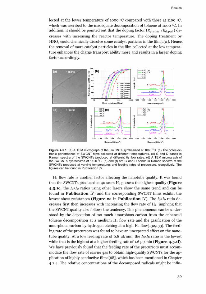
Results
39
lected at the lower temperature of 1000 oC compared with those at 1100 oC, which was ascribed to the inadequate decomposition of toluene at 1000 oC. In addition, it should be pointed out that the doping factor ( ) de-creases with increasing the reactor temperature. The doping treatment by HNO3 could chemically dissolve some catalyst particles in the film[131]. Hence, the removal of more catalyst particles in the film collected at the low tempera-ture enhances the charge transport ability more and results in a larger doping factor accordingly.
Figure 4.5.1. (a) A TEM micrograph of the SWCNTs synthesized at 1060 oC. (b) The optoelec-tronic performance of SWCNT films collected at different temperatures. (c) G and D bands in Raman spectra of the SWCNTs produced at different H2 flow rates. (d) A TEM micrograph of the SWCNTs synthesized at 1120 oC. (e) and (f) are G and D bands in Raman spectra of the SWCNTs produced at varying temperatures and feeding rates of precursors, respectively. The figures can be found in Publication .
H2 flow rate is another factor affecting the nanotube quality. It was found that the SWCNTs produced at 40 sccm H2 possess the highest quality (Figure 4.5.1c, the IG/ID ratios using other lasers show the same trend and can be found in Publication ) and the corresponding SWCNT films exhibit the lowest sheet resistances (Figure 2a in Publication ). The IG/ID ratio de-creases first then increases with increasing the flow rate of H2, implying that the SWCNT quality also follows the tendency. This phenomenon can be under-stood by the deposition of too much amorphous carbon from the enhanced toluene decomposition at a medium H2 flow rate and the gasification of the amorphous carbon by hydrogen etching at a high H2 flow[132,133]. The feed-ing rate of the precursors was found to have an unexpected effect on the nano-tube quality. At a low feeding rate of 0.8 μl/min, the IG/ID ratio is the lowest while that is the highest at a higher feeding rate of 1.6 μl/min (Figure 4.5.1f). We have previously found that the feeding rate of the precursors must accom-modate the flow rate of carrier gas to obtain high-quality SWCNTs for the ap-plication of highly conductive films[68], which has been mentioned in Chapter 4.2.4. The relative concentrations of the decomposed radicals might be influ-
(a)
(d)
1060 oC
1120 oC
1200 1300 1400 1500 1600 1700 1800
G
IG/ID=42.7
IG/ID=37.4
IG/ID=35.8
1060 oC 1080 oC 1100 oC 1120 oC
Inte
nsity
(a.u
.)
Raman shift (cm-1)
IG/ID=17.5D
(e)
1200 1300 1400 1500 1600 1700 1800
40 H2
50 H2
60 H2
70 H2
Inte
nsity
(a.u
.)
Raman shift (cm-1)
D
G
IG/ID=47.3
IG/ID=46.3
IG/ID=35.6
IG/ID=41.3
(c)
1200 1300 1400 1500 1600 1700 1800
D
0.8 μl 1.0 μl 1.3 μl 1.6 μl
Inte
nsity
(a.u
.)
Raman shift (cm-1)
IG/ID=63.8
IG/ID=44.1
IG/ID=47.3
IG/ID=43.3
G(f)
10 100 1000 1000080
84
88
92
96
100
1060 oC-pristine 1080 oC-pristine 1100 oC-pristine 1120 oC-pristine 1060 oC-doped 1080 oC-doped 1100 oC-doped 1120 oC-doped
Tran
smitt
ance
at 5
50 n
m (%
)
Sheet resistance (Ω/sq)
(b)
Results
40
enced by the flow rate of carrier gas. Further reduction of N2 and H2 flow rates are expected to produce SWCNTs with higher quality at the feeding rate of 0.8 μl/min. The more detailed discussion concerning the effects of the parameters on the nanotube quality can be found in Publication .
4.5.2 Tuning the diameters of SWCNT bundles
The study of an SWCNT TCF should always, at least, include the bundle di-ameters and lengths of SWCNTs, since those two factors can greatly influence the optoelectronic performance. In an aerosol reactor, the as-synthesized na-notubes in the gas phase can have more or less mutual collision caused by Brownian diffusion, and most of the bundles are formed in this way. Nanotube bundles can also form during the growth process due to the strong attraction of van der Waals forces among several independently growing nanotubes. In ad-dition, some floating bundles can re-bundle during the film formation on a membrane filter, since the film is formed through a gas-phase filtration process. Consequently, to study the bundle diameter, the diameter distribution of the SWCNT bundles in an actual as-formed film would be ideal. However, in a practical case, it is hard to measure the bundle diameters in a thick film though the measurement of the bundles in a film with the transmittance high-er than 97% with TEM would minimize the discrepancy. The thicker film in TEM can cause focus issues due to the variation of the height profiles of nano-tube bundles, leading to an increase in measurement error. AFM is another technique to check the bundle diameters by measuring the height profiles of sub-monolayer bundles situating on a silicon substrate. The tapping mode is usually adopted in the AFM scanning, thus compressing the nanotube bundles and inducing an underestimation of the bundle diameters accordingly. There-fore, TEM is the representative technique to study the bundle diameters. Even though there might exist a slight underestimation of the bundle diameters compared with those in an actual film, the trends shown in both cases should be the same.
In the toluene case, a low feeding rate of 0.8 μl/min and a higher feeding rate of 1.6 μl/min were selected to compare the bundle diameters. The TEM micrographs of the SWCNTs visually display the diameter difference of the SWCNT bundles (Figure 4.5.2a, b). Statistically gathering the nanotube bundles forms the histogram distributions of bundle diameters. The mean bundle diameters of the SWCNTs synthesized at the feeding rates of 0.8 μl/min and 1.6 μl/min are 6.4 nm and 8.8 nm, respectively (Figure 4.5.2d, e). It has been mentioned in Chapter 4.2.4 that the narrower bundles in an SWCNT film generate more charge transport routes and should behave better in terms of conductivity. However, the optoelectronic results presented here (see Figure 4f in Publication ) is in contrast to the general tendency. As discussed in the previous part on the effect of feeding rate on the nanotube quality, the quality of the SWCNTs is the lowest when adopting the low feeding rate of 0.8 μl/min while that is the highest at 1.6 μl/min. The flow rate of carri-er gas (both N2 and H2) should be decreased a bit to match the low feeding rate. Therefore, one is not recommended to claim that nanotube quality, diameter,

Results
41
length or the bundle diameter alone contributes most to the conductivity (or sheet resistance) of an SWCNT film. Furthermore, other factors should be ideally kept constant (or as close as possible) to investigate one of the factors. A more systematic experimental study of the growth parameters, combined with machine learning[134], might locate the optimal conditions to produce SWCNTs for the fabrication of TCFs with an optoelectronic performance ap-proaching or even outperforming that of ITO film.
Figure 4.5.2. (a) and (b) are TEM micrographs of the SWCNTs synthesized at the feeding rates of 0.8 μl/min and 1.6 μl/min, respectively. (c) An SEM micrograph of isolated SWCNT bundles for length measurement. The optimized feeding rate of 1 μl/min was utilized. (d) and (e) are diameter distributions of the SWCNT bundles collected at the feeding rates of 0.8 μl/min and 1.6 μl/min, respectively. (f) The length distribution of the nanotube bundles in (c). The figures are displayed in Publication .
The SWCNT length is another critical factor affecting the sheet resistance of a film. Here, we also measured SWCNT lengths since a new carbon source, i.e., toluene, was selected. We found that the mean length of the SWCNT bundles is up to 41.4 μm with a standard deviation of 21.5 μm (Figure 4.5.2f). The growth of such long SWCNTs may be on account of the fast growth speeds enabled by instant carbon feeding from toluene. Compared with the lengths of the SWCNTs synthesized from carbon monoxide[98], ethylene[69], or etha-nol[68] as the carbon source, it is suggested that the active hydrocarbon, here toluene, has the ability to provide adequate carbon atoms for the growth of long SWCNTs prior to the deactivation of catalyst particles out of the growth zone. As mentioned earlier in Chapter 4.2.4, long SWCNTs are always pre-ferred in TCF applications since the number of dominant resistance contribu-tors, i.e., contact junctions, is reduced in a film comprising long tubes.
4.5.3 Enhancing film conductivity by dopant
The conductivity of an as-fabricated SWCNT TCF is usually far away from the requirement of the device which needs high optoelectronic performance. Thus, chemical doping as the main strategy to enhance the film conductivity is needed, and the subsequent encapsulation of SWCNT films to prevent air and
0 4 8 12 16 20 24 280.00
0.05
0.10
0.15
0.20
0.25
0.30
0.35
Freq
uenc
y
Bundle diameter (nm)
Total: 142
0 4 8 12 16 20 24 280.00
0.05
0.10
0.15
0.20
0.25
Fr
eque
ncy
Bundle diameter (nm)
Total: 155
(b)
(e)
(a)
(d)
8.8 5.2nm6.4 3.5nm
0.8 μl/min 1.6 μl/min
0.8 μl/min 1.6 μl/min
0 10 20 30 40 50 60 70 80 90 1000.00
0.05
0.10
0.15
0.20
Freq
uenc
y
Bundle length (μm)
Total: 237(f)
41.4 21.5μm
10 μm
(c)
Results
42
moisture is imperative in the device fabrication process. Nitric acid (HNO3)[6,59,61,135] and gold chloride (AuCl3)[68,79,98,136] are two popular dopants utilized for doping CNTs. Via doping, the enhanced conductivity of SWCNTs is originated from decreasing the Schottky barrier between metallic and semiconducting nanotube contact junctions[137], shifting the Fermi level towards the valence band of nanotubes[79], and densifying the film[61]. HNO3 can also chemically dissolve the catalyst particles to improve the film conduc-tivity, which has been considered as one purification route[131]. Herein, Ra-man spectra of the pristine and doped SWCNTs were carefully analyzed to uncover the origin of the doping effect. As seen from the RBM peaks in Figure 4.5.3a, their intensities were suppressed after doping, indicating the related SWCNTs were doped. Moreover, the blue shift (to a high frequency) in the G band (Figure 4.5.3b) implies that both HNO3 and AuCl3 are p-type dopants which accept the electrons from nanotubes. It is worth noting that the G band in the Raman spectrum of AuCl3-doped SWCNTs has a larger shift compared to that in the HNO3-doped sample, revealing that AuCl3 is the stronger dopant for the SWCNTs produced in this work. The sheet resistance of the SWCNT TCF at 90% T was reduced to ca. 66 Ω/sq ( ) from the pristine value of ca. 143 Ω/sq ( ) through HNO3 treatment (Figure 4.5.3c). AuCl3 doping lowered the pristine value further to ca. 57 Ω/sq ( ) which is one of the lowest sheet resistances for the SWCNT TCFs at 90% T[59,69,97,138]. We have found that the doping ability, i.e., life time, of AuCl3 degrades with time if AuCl3 is stored under ambient conditions for one week (some precipitation can be observed), meaning the AuCl3 solution should be as fresh as possible for comparing doped resistances. Consequently, HNO3 was selected as the dopant throughout the optimization process since its concentration is constant (kept at 65 wt%). All in all, chemical doping of SWCNTs introduces extra atoms or impurities most probably. For instance, HNO3 as a strong acid can cause some structural defects[139] while AuCl3 treatment of SWCNTs brings about some gold particles[136]. The defects and impurities would ultimately impact device performance in certain applications. Therefore, a more stable and stronger dopant which has a weaker negative effect on SWCNTs should be adopted to meet the requirements of optoelec-tronic devices, such as solar cells[140], organic light-emitting diodes (OLEDs)[59]. Alternatively, the synthesis of metallic-enriched SWCNTs might be advantageous for their applications in transparent conductors[89].
4.5.4 Comparison of film performance and yield
To have a rough idea about how good the films are, the SWCNT films reported in this work and some other FCCVD-fabricated SWCNT films in the literature[59,68,69,97,98,138,141] were selected to compare with the repre-sentative TCFs made of graphene[142], silver nanowires[143], and ITO film[143] (Figure 4.5.3c). It is demonstrated that the optoelectronic perfor-mance of the SWCNT TCF reported in this work is comparable with those of TCFs made of other rigid materials. Additionally, SWCNT TCF has the advan-tages of low reflective index and maintaining electronic properties under me-
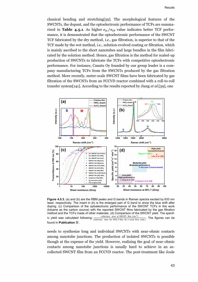
Results
43
chanical bending and stretching[59]. The morphological features of the SWCNTs, the dopant, and the optoelectronic performance of TCFs are summa-rized in Table 4.5.1. As higher value indicates better TCF perfor-mance, it is demonstrated that the optoelectronic performance of the SWCNT TCF fabricated by the dry method, i.e., gas filtration, is superior to that of the TCF made by the wet method, i.e., solution-evolved coating or filtration, which is mainly ascribed to the short nanotubes and large bundles in the film fabri-cated by the solution method. Hence, gas filtration is the method for scaled-up production of SWCNTs to fabricate the TCFs with competitive optoelectronic performance. For instance, Canatu Oy founded by our group leader is a com-pany manufacturing TCFs from the SWCNTs produced by the gas filtration method. More recently, meter-scale SWCNT films have been fabricated by gas filtration of the SWCNTs from an FCCVD reactor combined with a roll-to-roll transfer system[141]. According to the results reported by Jiang et al.[59], one
Figure 4.5.3. (a) and (b) are the RBM peaks and G bands in Raman spectra excited by 633 nm laser, respectively. The insert in (b) is the enlarged part of G band to show the blue shift after doping. (c) Comparison of the optoelectronic performance of the SWCNT TCFs in this work (toluene as the carbon source) with the reported SWCNT films fabricated by the gas filtration method and the TCFs made of other materials. (d) Comparison of the SWCNT yield. The specif-ic yield was calculated following: . The figures can be found in Publication .
needs to synthesize long and individual SWCNTs with near-ohmic contacts among nanotube junctions. The production of isolated SWCNTs is possible though at the expense of the yield. However, realizing the goal of near-ohmic contacts among nanotube junctions is usually hard to achieve in an as-collected SWCNT film from an FCCVD reactor. The post-treatment like Joule
1 10 100 1000 100000
20
40
60
80
100
Our SWCNT film-Pristine Our SWCNT film-HNO3
Our SWCNT film-AuCl3 SWCNT film [98]-AuCl3 SWCNT film [68]-AuCl3 SWCNT film [141]-HNO3
SWCNT film [97]-HNO3
SWCNT film [69]-HNO3
SWCNT film [138]-HAuCl4 SWCNT film [59]- HNO3
Graphene [142]-HNO3
Ag nanowires [143] ITO on glass [143]
Tran
smitt
ance
at 5
50 n
m (%
)
Sheet resistance (Ω/sq)
(c)
100 150 200 250 300
Pristine film HNO3-doped AuCl3-doped
Inte
nsity
(a.u
.)
Raman shift (cm-1)
1200 1400 1600 2600 2800
G'
G
D
Pristine film HNO3-doped
AuCl3-doped
Inte
nsity
(a.u
.)
Raman shift (cm-1)
1560 1580 1600 1620 1640 1660
1611
1617
1624
S M (b)
(a)
(d) High yieldLow performance
Moderate yieldModerate performance
Low yieldHigh performance
20 30 40 50 60 70 80 90 1000
2
4
6
8
10
12
14
16
18
Jiang et al. [59] Hussain et al. [69]
Our work [Toluene-based]
Ding et al. [68] Liao et al. [98]
Spec
ific
yiel
d (c
m2 ·h
-1·s
lm-1
)
Sheet resistance at 90% T (Ω/sq)

Results
44
heating of the film in an inert gas atmosphere might weld the nanotubes to-gether at the junction parts to facilitate the transport of charge carriers[147].
Table 4.5.1. Summary of the morphological features of as-synthesized SWCNTs and the optoe-lectronic performance of corresponding TCFs after doping treatment.
Fabrication method
Dt(nm)
L(μm)
Dbun
dle(nm)
Substrate
Dopant Rpristine(Ω/sq)
Rdoped(Ω/sq)
T550(%)
Reference
Spin coating
- - - Glass HNO3+SOCl2
- 59 71 17.1 [63]
Spray coating
- - - PET HNO3 400 170 90 20.5 [61]
Rod coating
- - - PET HNO3 500 160 90 21.8 [64]
Gas filtration
1.26 4.2 3.5 Quartz AuCl3 469 116 90 30.0
Gas filtration+grid
1.35 - - PEN HNO3 - 53 80 30.1 [144]
Gas filtration
1.45 9.4 12.8 PET HNO3 820 110 90 31.6 [6]
Gas filtration
1.82 27.4 6.3 Quartz AuCl3 440 95 90 36.6
Gas filtration
1.3 4.8 3.5 PEN HNO3 950 89 90 39.1 [93]
Gas filtration
1.9 7.5 7.1 Quartz AuCl3 273.4 86.8 90 40.1 [98]
Gas filtration
- ~10 - PET NO2 300 84 90 41.4 [58]
Gas filtration
2.0 28.4 5.3 Quartz AuCl3 360 78 90 44.6
TP collection
2.0 7.6 - PET AuCl3 390 76 90 45.8 [145]
Gas filtration
1.7~2.4
20 - PET HNO3 200 65 90 53.6 [141]
Gas filtration
1.1 4 1.21 Quartz HNO3 - 63 90 55.3 [97]
Gas filtration
2.3 41.4 ~7 PET AuCl3 143 57 90 61.1
Aerosol doping
2 - - PET HAuCl4 485 36 85 61.8 [146]
Liquid filtration
- - - PET HSO3Cl - 60 90.9 64.2 [67]
Gas filtration
1.3 13 4 Quartz HNO3 195 51 90 68.3 [69]
Doping study
- - - PET HAuCl4 ~600 40 90 87.0 [138]
Gas filtration
2.0 62 85% isolated
PET HNO3 41 25 90 139.2 [59]
Note: 1. “TP” stands for the thermophoretic precipitator which is a plate system designed for the collection of CNTs or other aerosol particles. 2. A gird method is used to increase the transpa-rency of CNT film while keeping low sheet resistance simultaneously by depositing a dense film. 3. Dt is the mean diameter of SWCNTs, L is the mean length of SWCNTs, Dbundle is the mean diameter of SWCNT bundles, Rpristine and Rdoped are the sheet resistances of pristine and doped SWCNT TCFs, respectively, T550 is the transmittance value obtained at 550 nm. 4. “–” means the relevant data are not available in the literature. 5. PEN and PET stand for polyethylene naphthalate and polyethylene terephthalate, respectively. 6. , , and refer to Publica-tion , Publication , Publication and Publication , respectively.
To qualitatively assess SWCNT yield, the result in this work was compared with those reported in the literature[59,68,69,98] (Figure 4.5.3d). Here, the specific yield was utilized for the comparison. Considering the comparable optoelectronic performance of SWCNT TCFs, the yield in this work is 7.5 times higher than that in ethylene case[69], and around 12 times higher than that of SWCNTs synthesized from ethanol at the feeding rate of 2 μl/min (evaluated
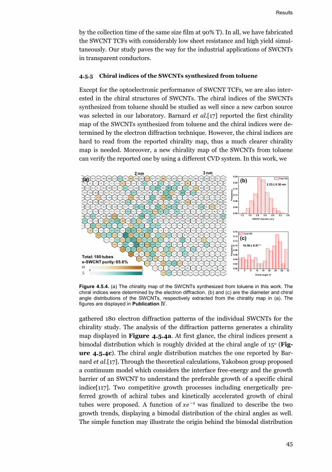
Results
45
by the collection time of the same size film at 90% T). In all, we have fabricated the SWCNT TCFs with considerably low sheet resistance and high yield simul-taneously. Our study paves the way for the industrial applications of SWCNTs in transparent conductors.
4.5.5 Chiral indices of the SWCNTs synthesized from toluene
Except for the optoelectronic performance of SWCNT TCFs, we are also inter-ested in the chiral structures of SWCNTs. The chiral indices of the SWCNTs synthesized from toluene should be studied as well since a new carbon source was selected in our laboratory. Barnard et al.[17] reported the first chirality map of the SWCNTs synthesized from toluene and the chiral indices were de-termined by the electron diffraction technique. However, the chiral indices are hard to read from the reported chirality map, thus a much clearer chirality map is needed. Moreover, a new chirality map of the SWCNTs from toluene can verify the reported one by using a different CVD system. In this work, we
Figure 4.5.4. (a) The chirality map of the SWCNTs synthesized from toluene in this work. The chiral indices were determined by the electron diffraction. (b) and (c) are the diameter and chiral angle distributions of the SWCNTs, respectively extracted from the chirality map in (a). The figures are displayed in Publication .
gathered 180 electron diffraction patterns of the individual SWCNTs for the chirality study. The analysis of the diffraction patterns generates a chirality map displayed in Figure 4.5.4a. At first glance, the chiral indices present a bimodal distribution which is roughly divided at the chiral angle of 15o (Fig-ure 4.5.4c). The chiral angle distribution matches the one reported by Bar-nard et al.[17]. Through the theoretical calculations, Yakobson group proposed a continuum model which considers the interface free-energy and the growth barrier of an SWCNT to understand the preferable growth of a specific chiral indice[117]. Two competitive growth processes including energetically pre-ferred growth of achiral tubes and kinetically accelerated growth of chiral tubes were proposed. A function of was finalized to describe the two growth trends, displaying a bimodal distribution of the chiral angles as well. The simple function may illustrate the origin behind the bimodal distribution
1.2 1.6 2.0 2.4 2.8 3.2 3.60.00
0.04
0.08
0.12
0.16
0.20
0.24
Freq
uenc
y
SWCNT diameter (nm)
Total:180
0 4 8 12 16 20 24 28 320.00
0.02
0.04
0.06
0.08
0.10
0.12
0.14
0.16
Fr
eque
ncy
Chiral angle (o)
Total:180
2.23 0.36 nm
18.56 8.97 o
(a) (b)
(c)
Total: 180 tubess-SWCNT purity: 65.6%
2 nm 3 nm
Results
46
of the chiralities observed in our work. More detailed discussions can be found in Publication and the reference[117]. Besides, as the armchair tubes overcome lower energy barrier for the nucleation compared with the zigzag counterparts[117], the near armchair tubes behave a prevalence and account for 67.8% out of 180 tubes. Using ethanol[25] as the carbon source, the ma-jority of the chiral indices of as-collected SWCNTs are close to armchair type. Thus, the chirality distribution shown here might support the etching proposal which holds that the unstable near-zigzag tubes can be etched away by the oxygen-containing radicals like OH decomposed from ethanol[25]. Further-more, the purity of the s-SWCNTs produced from toluene is 65.6% which is ca. 10% lower than that of the s-SWCNTs synthesized from ethanol[25], which could be also caused by the etching of small-diameter metallic tubes[88,115]. In addition, the diameters of the SWCNTs were extracted from the chirality map and constitute the histogram distribution of diameters. The mean diame-ter of the SWCNTs was found to be ca. 2.23 nm (Figure 4.5.4b) which is con-sistent with that (ca. 2.32 nm) fitted from the absorption spectrum (see Fig-ure S10 in Publication ). The large-diameter SWCNTs could also enhance the conductivity of the corresponding TCFs since numerous charge carriers can be excited in virtue of their narrow band gaps[148]. The chirality map in Figure 4.5.4a can serve as a reference for those SWCNTs synthesized from toluene in spite of the diversity of CVD systems for nanotube production.
4.6 Production of semiconducting-enriched SWCNTs
Apart from improving the conductivity of SWCNT TCFs, selective growth, e.g., chirality, metallicity, of SWCNTs is also a meaningful research topic for the moment. Especially, semiconducting SWCNTs (s-SWCNTs) are drawing in-creasing attention due to the existence of variable band gaps and have been applied in many semiconductor fields like digital electronics[18], thermoelec-tric generators[19], photovoltaics[20]. Most recently, a milestone accom-plishment that a 16-bit computer was built entirely from CNT transistors using s-SWCNTs with the purity of 99.99% has been achieved by Shulaker group[149]. The computer was able to output the message of “Hello, World” by running a simple program. Therefore, the production of s-SWCNTs with high purity (>95%) is of significant meaning for the semiconductor devices.
To produce s-SWCNTs, solution-evolved separation and substrate CVD growth are two dominant methods at the moment. Among them, solution se-paration is more popular on account of the advantages of high-purity s-SWCNTs and scaled-up production. The s-SWCNT purity of ca. 99.997% de-termined by the high throughout electrical testing has been achieved by the polymer-assisted extraction method[21]. With a film coating technique[66], e.g., spray coating, dip coating, roll-to-roll coating, the s-SWCNTs in a solution can be coated onto many smooth substrates for large-scale applications[150]. Nevertheless, the solution process is too time-consuming, including repeated sonication, ultracentrifugation, and separation procedures. The major chal-lenge, thus, for the separated s-SWCNTs is that their lengths are usually short-
Results
47
er than 2 μm[21,151]. As for the direct growth of s-SWCNTs by the substrate CVD method, the yield of s-SWCNTs is pretty low (even invisible by naked eyes)[151], limiting their scaled-up applications. Furthermore, the as-grown s-SWCNTs have to be transferred to some temperature-sensitive substrates for the applications of flexible devices, introducing structural defects in the trans-fer process[152]. Hence, a simple, one-step method is needed to produce s-SWCNTs on a large scale.
As was inspired by the semiconducting ratio of 76.8% described in Chapter 4.3, we were encouraged to adopt ethanol as the carbon source and optimize the growth parameters further to synthesize s-SWCNTs on a pilot scale using our FCCVD reactor. Herein, methanol was selected as an additive to enhance the growth of s-SWCNTs. The effect of methanol amount was selectively dis-cussed through optical characterizations in the dissertation.
4.6.1 The effect of methanol amount
Optical absorption characterization is a fast and easily accessible technique for relatively comprehensive understanding of SWCNTs. Therefore, the optimiza-tion of the growth parameters targeting high-purity s-SWCNTs was mainly based on the analysis of the optical absorption spectra. To minimize the effect of ambient doping on SWCNTs, all the absorption spectra were acquired im-mediately upon taking out the film sample from the reactor downstream (air exposure time throughout the whole process was around two minutes). We have reported a semiconducting ratio of 76.8% in our previous work using ethanol as the carbon source[25]. Meanwhile, it has been suggested that me-thanol, as a weak etchant, has the potential to enrich s-SWCNTs by preferen-tially etching some metallic tubes[116]. Thus, methanol was selected as a growth enhancer for s-SWCNT production in this work, as it is easily miscible in ethanol and the concentration can be finely tuned due to the gentle oxida-tion ability. The purity of the s-SWCNTs synthesized without methanol is rela-tively low compared with those obtained with the addition of a suitable amount of methanol, though excess methanol decreases the purity (Figure 4.6.1a, b). The purity of the s-SWCNTs synthesized at the optimal conditions was calculated to be higher than 95% (Figure 4.6.1b). Besides, it should be pointed out that the width of S11 peak in the absorption spectrum shrinks and the height rises with the addition of methanol. By fitting the absorption spec-tra to obtain the corresponding diameter distributions, the proportion of nar-row-diameter SWCNTs was found to reduce after adding an excess amount of methanol, though the mean diameter only has a slight shift from ca. 1.29 nm (0 v% methanol) to ca. 1.31 nm (18 v% methanol). A semiconducting-enriched SWCNT film displaying light green color on a 13 mm membrane filter is pre-sented in Figure 4.6.1b to demonstrate the scalability of our reactor. The comparison of RBM features (Figure 4.6.1c-f) indicates the disappearance of some near-zigzag SWCNTs with the addition of an appropriate volume of me-thanol.
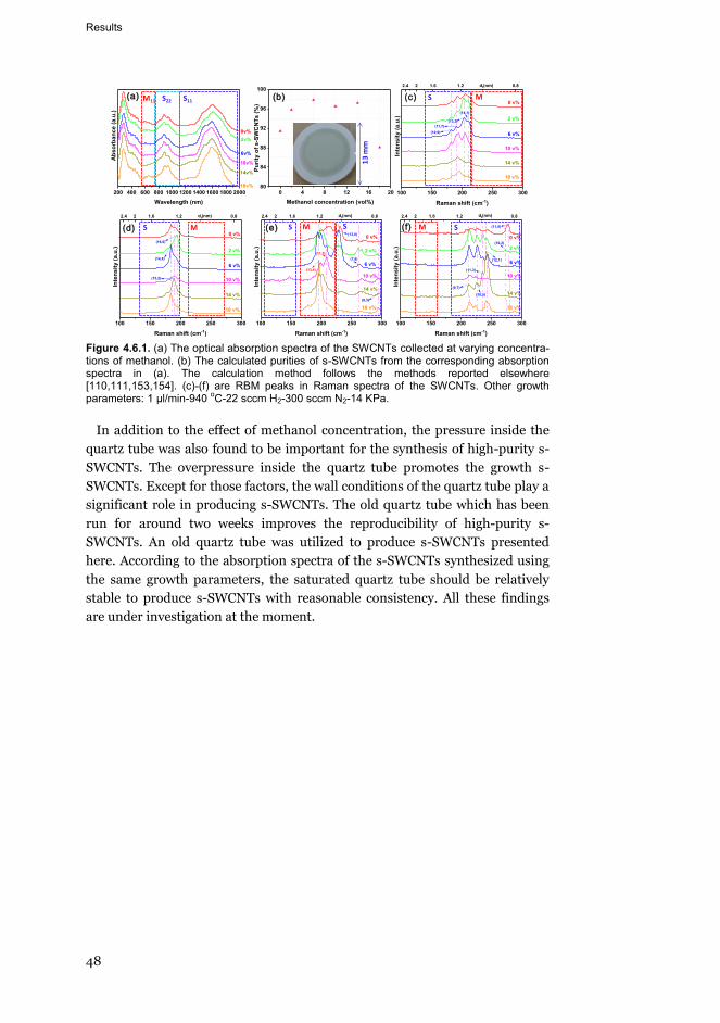
Results
48
Figure 4.6.1. (a) The optical absorption spectra of the SWCNTs collected at varying concentra-tions of methanol. (b) The calculated purities of s-SWCNTs from the corresponding absorption spectra in (a). The calculation method follows the methods reported elsewhere [110,111,153,154]. (c)-(f) are RBM peaks in Raman spectra of the SWCNTs. Other growth parameters: 1 μl/min-940 oC-22 sccm H2-300 sccm N2-14 KPa.
In addition to the effect of methanol concentration, the pressure inside the quartz tube was also found to be important for the synthesis of high-purity s-SWCNTs. The overpressure inside the quartz tube promotes the growth s-SWCNTs. Except for those factors, the wall conditions of the quartz tube play a significant role in producing s-SWCNTs. The old quartz tube which has been run for around two weeks improves the reproducibility of high-purity s-SWCNTs. An old quartz tube was utilized to produce s-SWCNTs presented here. According to the absorption spectra of the s-SWCNTs synthesized using the same growth parameters, the saturated quartz tube should be relatively stable to produce s-SWCNTs with reasonable consistency. All these findings are under investigation at the moment.
100 150 200 250 300
(10,2)
Inte
nsity
(a.u
.)
Raman shift (cm-1)
2.4 2 1.6 1.2 0.8
(11,0)
(9,7)
(10,5)
(12,1)
dt(nm)
18 v%
14 v%
10 v%
6 v%
2 v%
0 v%
(11,3)
0 4 8 12 16 2080
84
88
92
96
100
Purit
y of
s-S
WC
NTs
(%)
Methanol concentration (vol%)
S11S22M11
SM
100 150 200 250 300
18 v%
14 v%
10 v%
6 v%
2 v%
0 v%
(11,7)(13,3)
Inte
nsity
(a.u
.)
Raman shift (cm-1)
(14,1)
(10,9)
2.4 2 1.6 1.2 0.8dt(nm)
S M
13 m
m
200 400 600 800 1000 1200 1400 1600 1800 200018v%
2v%
6v%
0v%
14v%
10v%
Abs
orba
nce
(a.u
.)
Wavelength (nm)
100 150 200 250 300
Inte
nsity
(a.u
.)
Raman shift (cm-1)
2.4 2 1.6 1.2 0.8dt(nm)
18 v%
14 v%
10 v%
6 v%
2 v%
0 v%
(15,2)
(16,0)
(14,4)
S M
100 150 200 250 300
Inte
nsity
(a.u
.)
Raman shift (cm-1)
2.4 2 1.6 1.2 0.8
(13,4)
(13,0)
(11,5)
(8,3)
dt(nm)
18 v%
14 v%
10 v%
6 v%
2 v%
0 v%
(7,6)
M SS
49
5. Conclusion and outlook
The work of this dissertation demonstrates the first results on the applications of SWCNTs synthesized from ethanol and toluene separately as the carbon source in the field of TCFs and continuous production of semiconducting-enriched SWCNTs by the FCCVD method. The primary objective was to manif-est the ability of liquid carbon source, i.e., ethanol and toluene, to synthesize good-quality SWCNTs with high yield for the rapid fabrication of highly con-ductive TCFs. Specifically, we targeted to improve the optoelectronic perfor-mance of SWCNT TCFs and the purity of s-SWCNTs via optimizing the growth parameters.
First, an inexpensive and environmental-friendly liquid hydrocarbon com-pound, ethanol, was chosen to be the carbon source for SWCNT synthesis with a newly-built FCCVD reactor. The various growth parameters were optimized with respect to the optoelectronic performance of TCFs. SWCNT TCF with a low sheet resistance of ca. 78 Ω/sq at 90% T was obtained with a reasonable yield. The distinct finding compared with other studies is the mean length of the SWCNT bundles reaches 28.4 μm which is particularly beneficial for the fabrication of stretchable electronics. What is worthy to be mentioned is the chiral indices of the SWCNTs clustered around armchair edge were deter-mined by the electron diffraction technique.
Then, a spark-discharge FCCVD reactor was utilized to investigate the roles of sulfur in SWCNT growth. We found that sulfur can increase the SWCNT yield, diameter, length, and can improve nanotube quality. The optoelectronic performance of the SWCNT TCF collected with the addition of an optimal amount of sulfur exhibits a sheet resistance of ca. 116 Ω/sq at 90% T which is almost half of the value for the TCFs obtained without sulfur. We suggested that sulfur with an appropriate concentration promotes the formation of active sites on the catalyst surface to enhance SWCNT growth.
Since the yield of as-produced SWCNTs decreased a lot in ethanol case when lower sheet resistances of TCFs were expected, an alternative carbon source may address the yield issue. Then, toluene was selected to be another liquid carbon source. The growth parameters were carefully investigated as well in the toluene case. A remarkably low sheet resistance of ca. 57 Ω/sq at 90% T was achieved for the SWCNT TCFs. It should be pointed out that the yield in the toluene case is around 12 times higher than that in the ethanol case, consi-dering the comparable optoelectronic performance. The mean length of the SWCNT bundles is as long as 41.4 μm. By electron diffraction analysis, a chi-

Conclusion and outlook
50
rality map displaying a bimodal distribution of the chiral angles was generated. The chirality distribution of the SWCNTs verifies the theoretical prediction proposed by the Yakobson group. The work using toluene as the carbon source has laid a solid foundation for the industrial-level application of SWCNTs. When it comes to the industrial-level production, the flow rates of N2 and H2, and the feeding rate of precursor solution should be scaled with the diameter of the quartz tube used, while the recipe of precursor solution can be copied from this work. In addition, the stability and durability of the pilot reactor to-gether with the cost should be taken into account.
Except for improving the optoelectronic performance of TCFs, selective growth of s-SWCNTs was also carried out using ethanol as the carbon source. Methanol was added to be a promoter for s-SWCNT growth. With the addition of an optimal volume of methanol, the purity of s-SWCNTs can be higher than 95% calculated from the absorption spectrum. The continuous production of semiconducting-enriched SWCNTs demonstrated here has significant mean-ing for the application of s-SWCNTs in large-area flexible and stretchable sem-iconductor devices, e.g., OLED.
In terms of the optoelectronic performance of SWCNT TCFs, there is still some room to be improved. One needs to be very careful with the growth pa-rameters and should keep in mind that the feeding rate of the precursors must accommodate the flow rates of carrier gases, e.g., N2 and H2. There may exist other optimal parameters, thus investigating more parameter combinations probably locate another region for further lowered sheet resistances. Decreas-ing the feeding rate of the precursors induces the production of more individu-al SWCNTs and lower film sheet resistances accordingly, which is also benefi-cial for the fabrication of TFTs. Machine learning could be combined with a series of experimental data sets (the data from several variables with each of the other parameters fixed) to accelerate the optimization of growth parame-ters targeting high-performance SWCNT TCFs. Additionally, a systematic in-vestigation of SWCNT doping may improve the TCF performance via optimiz-ing the doping process, e.g., in-situ gas-phase doping of as-formed SWCNTs in the synthesis reactor, and/or selecting a stronger dopant, e.g., HAuCl4. Re-garding the mechanism study, H2 effect on the morphological and structural features of SWCNTs should be given special care. Independent experimental investigations particularly combined with theoretical simulations on the H2 effect can be carried out. Theoretical studies on sulfur effect are also helpful for the understanding of the sulfur role in SWCNT growth at the atomic scale.
To further raise the purity of s-SWCNTs, the feeding rate of the precursors can be decreased a bit with appropriate flow rates of N2 and H2. The growth temperature can also be moderately adjusted. Except for methanol, other oxy-gen-containing compounds like isopropanol, H2O, CO2 with a finely controlled concentration may be considered to be an additive to the recipe for the synthe-sis of s-SWCNTs by the FCCVD method. The repeatability of the s-SWCNT synthesis, especially the roles of the reactions at the quartz tube wall, needs to be further studied. Additionally, magnet-assisted separation of s-SWCNTs and the metallic counterparts could be tried if individual SWCNTs are dominant in

Conclusion and outlook
51
the synthesis reactor. The alignment of as-produced s-SWCNTs from the reac-tor outlet using the thermophoretic collection system can be tested as well, which is meaningful for the high-current electronics.
52
References
[1] R.H. Baughman, A.A. Zakhidov, W.A. De Heer, Carbon nanotubes-the route toward applications, Science. 297 (2002) 787–792.
[2] M.W. Rowell, M.A. Topinka, M.D. McGehee, H.J. Prall, G. Dennler, N.S. Sariciftci, L. Hu, G. Gruner, Organic solar cells with carbon nanotube network electrodes, Appl. Phys. Lett. 88 (2006) 233-506.
[3] D.S. Hecht, D. Thomas, L. Hu, C. Ladous, T. Lam, Y. Park, G. Irvin, P. Drzaic, Carbon-nanotube film on plastic as transparent electrode for resistive touch screens, J. Soc. Inf. Disp. 17 (2009) 941-946.
[4] D. Zhang, K. Ryu, X. Liu, E. Polikarpov, J. Ly, M.E. Tompson, C. Zhou, Transparent, conductive, and flexible carbon nanotube films and their application in organic light-emitting diodes, Nano Lett. 6 (2006) 1880–1886.
[5] S. Park, M. Vosguerichian, Z. Bao, A review of fabrication and applications of carbon nanotube film-based flexible electronics, Nanoscale. 5 (2013) 1727–1752.
[6] A. Kaskela, A.G. Nasibulin, M.Y. Timmermans, B. Aitchison, A. Papadimitratos, Y. Tian, Z. Zhu, H. Jiang, D.P. Brown, A. Zakhidov, E.I. Kauppinen, Aerosol-synthesized SWCNT networks with tunable conductivity and transparency by a dry transfer technique, Nano Lett. 10 (2010) 4349–4355.
[7] Q. Cao, S.J. Han, G.S. Tulevski, A.D. Franklin, W. Haensch, Evaluation of field-effect mobility and contact resistance of transistors that use solution-processed single-walled carbon nanotubes, ACS Nano. 6 (2012) 6471–6477.
[8] D.M. Sun, M.Y. Timmermans, Y. Tian, A.G. Nasibulin, E.I. Kauppinen, S. Kishimoto, T. Mizutani, Y. Ohno, Flexible high-performance carbon nanotube integrated circuits, Nat. Nanotechnol. 6 (2011) 156–161.
[9] Y.-L. Li, I.A. Kinloch, A.H. Windle, Direct spinning of carbon nanotube fibers from chemical vapor deposition synthesis, Science. 304 (2004) 276–278.
[10] W. Xu, Y. Chen, H. Zhan, J.N. Wang, High-strength carbon nanotube film from improving alignment and densification, Nano Lett. 16 (2016) 946–952.
[11] R. Bhowmick, B.M. Clemens, B.A. Cruden, Parametric analysis of chirality families and diameter distributions in single-wall carbon nanotube production by the floating catalyst method, Carbon. 46 (2008) 907–922.
[12] A.G. Nasibulin, A. Moisala, H. Jiang, E.I. Kauppinen, Carbon nanotube synthesis from alcohols by a novel aerosol method, J. Nanoparticle Res. 8 (2006) 465–475.
[13] S.D. Shandakov, M.S. Rybakov, A.V. Kosobutsky, O.G. Sevostyanov, N.S. Zvidentsova, A.N. Gutov, M.V. Lomakin, I.V. Anoshkin, Controllable growth of single-walled carbon nanotubes by ethanol-ferrocene aerosol method, Nanotechnologies Russ. 7 (2012) 370–376.
[14] S.D. Shandakov, A.V. Kosobutsky, O.G. Sevostyanov, M.V. Lomakin, M.S. Rybakov, D.M. Russakov, Analysis of the efficiency of CVD synthesis of carbon nanotubes by the aerosol method based on ethanol, Russ. Phys. J. 58 (2015) 1028–1031.
[15] C. Paukner, K.K.K. Koziol, Ultra-pure single wall carbon nanotube fibres continuously spun without promoter, Sci. Rep. 4 (2014) 1–7.
[16] B. Alemán, M.M. Bernal, B. Mas, E.M. Pérez, V. Reguero, G. Xu, Y. Cui, J.J. Vilatela, Inherent predominance of high chiral angle metallic carbon nanotubes in continuous fibers grown from a molten catalyst, Nanoscale. 8 (2016) 4236–4244.
[17] J.S. Barnard, C. Paukner, K.K. Koziol, The role of carbon precursor on carbon nanotube chirality in floating catalyst chemical vapour deposition, Nanoscale. 8 (2016) 17262–17270.

References
53
[18] J. Tang, Q. Cao, G. Tulevski, K.A. Jenkins, L. Nela, D.B. Farmer, S.J. Han, Flexible CMOS integrated circuits based on carbon nanotubes with sub-10 ns stage delays, Nat. Electron. 1 (2018) 191–196.
[19] A.D. Avery, B.H. Zhou, J. Lee, E.S. Lee, E.M. Miller, R. Ihly, D. Wesenberg, K.S. Mistry, S.L. Guillot, B.L. Zink, Y.H. Kim, J.L. Blackburn, A.J. Ferguson, Tailored semiconducting carbon nanotube networks with enhanced thermoelectric properties, Nat. Energy. 1 (2016) 16033.
[20] R. Ihly, A.M. Dowgiallo, M. Yang, P. Schulz, N.J. Stanton, O.G. Reid, A.J. Ferguson, K. Zhu, J.J. Berry, J.L. Blackburn, Efficient charge extraction and slow recombination in organic-inorganic perovskites capped with semiconducting single-walled carbon nanotubes, Energy Environ. Sci. 9 (2016) 1439–1449.
[21] T. Lei, L.-L. Shao, Y.-Q. Zheng, G. Pitner, G. Fang, C. Zhu, S. Li, R. Beausoleil, H.-S.P. Wong, T.-C. Huang, K.-T. Cheng, Z. Bao, Low-voltage high-performance flexible digital and analog circuits based on ultrahigh-purity semiconducting carbon nanotubes, Nat. Commun. 10 (2019) 2161.
[22] J. Wang, X. Jin, Z. Liu, G. Yu, Q. Ji, H. Wei, J. Zhang, K. Zhang, D. Li, Z. Yuan, J. Li, P. Liu, Y. Wu, Y. Wei, J. Wang, Q. Li, L. Zhang, J. Kong, S. Fan, K. Jiang, Growing highly pure semiconducting carbon nanotubes by electrotwisting the helicity, Nat. Catal. 1 (2018) 326–331.
[23] X. Zhao, Y. Liu, S. Inoue, T. Suzuki, R.O. Jones, Y. Ando, Smallest carbon nanotube is 3 Å in diameter , Phys. Rev. Lett. 92 (2004) 125502.
[24] S. Lebedkin, P. Schweiss, B. Renker, S. Malik, F. Hennrich, M. Neumaier, C. Stoermer, M.M. Kappes, Single-wall carbon nanotubes with diameters approaching 6 nm obtained by laser vaporization, Carbon. 40 (2002) 417–423.
[25] E.X. Ding, H. Jiang, Q. Zhang, Y. Tian, P. Laiho, A. Hussain, Y. Liao, N. Wei, E.I. Kauppinen, Highly conductive and transparent single-walled carbon nanotube thin films from ethanol by floating catalyst chemical vapor deposition, Nanoscale. 9 (2017) 17601–17609.
[26] G. Dresselhaus, M.S. Dresselhaus, R. Saito, Physical properties of carbon nanotubes, World Scientific, (1998) ISBN 1783262419, 9781783262410.
[27] P.R. Wallace, The band theory of graphite, Phys. Rev. 71 (1947) 622–634. [28] T.W. Odom, J.-L. Huang, P. Kim, C.M. Lieber, Structure and Electronic
Properties of Carbon Nanotubes, J. Phys. Chem. B. 104 (2000) 2794–2809. [29] P.G. Collins, P. Avouris, Chapter 3 The electronic properties of carbon
nanotubes, Contemp. Concepts Condens. Matter Sci. 3 (2008) 49–81. [30] P. Avouris, Molecular electronics with carbon nanotubes, Acc. Chem. Res. 35
(2002) 1026–1034. [31] R. Saito, G. Dresselhaus, Trigonal warping effect of carbon nanotubes, Phys.
Rev. B-Condens. Matter Mater. Phys. 61 (2000) 2981–2990. [32] H. Kataura, Y. Kumazawa, Y. Maniwa, I. Umezu, S. Suzuki, Y. Ohtsuka, Y.
Achiba, Optical properties of single-wall carbon nanotubes, Synth. Met. 103 (1999) 2555–2558.
[33] Y. Tian, H. Jiang, J.V. Pfaler, Z. Zhu, A.G. Nasibulin, T. Nikitin, B. Aitchison, L. Khriachtchev, D.P. Brown, E.I. Kauppinen, Analysis of the size distribution of single-walled carbon nanotubes using optical absorption spectroscopy, J. Phys. Chem. Lett. 1 (2010) 1143–1148.
[34] B.J. Landi, H.J. Ruf, C.M. Evans, C.D. Cress, R.P. Raffaelle, Purity assessment of single-wall carbon nanotubes, using optical absorption spectroscopy, J. Phys. Chem. B. 109 (2005) 9952–9965.
[35] Y. Tian, H. Jiang, I. V. Anoshkin, L.J.I. Kauppinen, K. Mustonen, A.G. Nasibulin, E.I. Kauppinen, A reference material of single-walled carbon nanotubes: quantitative chirality assessment using optical absorption spectroscopy, RSC Adv. 5 (2015) 102974–102980.
[36] M. Pfohl, D.D. Tune, A. Graf, J. Zaumseil, R. Krupke, B.S. Flavel, Fitting single-walled carbon nanotube optical spectra, ACS Omega. 2 (2017) 1163–1171.
[37] G.A. Rance, D.H. Marsh, R.J. Nicholas, A.N. Khlobystov, UV-vis absorption spectroscopy of carbon nanotubes: Relationship between the π-electron plasmon and nanotube diameter, Chem. Phys. Lett. 493 (2010) 19–23.
References
54
[38] V.N. Popov, Curvature effects on the structural, electronic and optical properties of isolated single-walled carbon nanotubes within a symmetry-adapted non-orthogonal tight-binding model, New J. Phys. 6 (2004) 17.
[39] F. Wang, M.Y. Sfeir, L. Huang, X.M.H. Huang, Y. Wu, J. Kim, J. Hone, S. O’Brien, L.E. Brus, T.F. Heinz, Interactions between individual carbon nanotubes studied by Rayleigh scattering spectroscopy, Phys. Rev. Lett. 96 (2006) 167401.
[40] M.S. Dresselhaus, G. Dresselhaus, R. Saito, A. Jorio, Raman spectroscopy of carbon nanotubes, Phys. Rep. 409 (2005) 47–99.
[41] S.M. Bachilo, M.S. Strano, C. Kittrell, R.H. Hauge, R.E. Smalley, R.B. Weisman, Structure-assigned optical spectra of single-walled carbon nanotubes, Science. 298 (2002) 2361–2366.
[42] Y. Tian, H. Jiang, P. Laiho, E.I. Kauppinen, Validity of measuring metallic and semiconducting single-walled carbon nanotube fractions by quantitative Raman spectroscopy, Anal. Chem. 90 (2018) 2517–2525.
[43] Y. Piao, J.R. Simpson, J.K. Streit, G. Ao, M. Zheng, J.A. Fagan, A.R.H. Walker, Intensity ratio of resonant Raman modes for (n,m) enriched semiconducting carbon nanotubes, ACS Nano. 10 (2016) 5252–5259.
[44] A.M. Rao, J. Chen, E. Richter, U. Schlecht, P.C. Eklund, R.C. Haddon, U.D. Venkateswaran, Y.K. Kwon, D. Tománek, Effect of van der Waals interactions on the Raman modes in single walled carbon nanotubes, Phys. Rev. Lett. 86 (2001) 3895–3898.
[45] M.J. O’Connell, S. Sivaram, S.K. Doorn, Near-infrared resonance Raman excitation profile studies of single-walled carbon nanotube intertube interactions: A direct comparison of bundled and individually dispersed HiPco nanotubes, Phys. Rev. B-Condens. Matter Mater. Phys. 69 (2004) 235415.
[46] A. Moisala, A.G. Nasibulin, E.I. Kauppinen, The role of metal nanoparticles in the catalytic production of single-walled carbon nanotubes—a review, J. Phys. Condens. Matter. 15 (2003) S3011–S3035.
[47] W. Zhou, Z. Han, J. Wang, Y. Zhang, Z. Jin, X. Sun, Y. Zhang, C. Yan, Y. Li, Copper catalyzing growth of single-walled carbon nanotubes on substrates, Nano Lett. 6 (2006) 2987–2990.
[48] V. Jourdain, C. Bichara, Current understanding of the growth of carbon nanotubes in catalytic chemical vapour deposition, Carbon. 58 (2013) 2–39.
[49] E.-X. Ding, J. Wang, H.-Z. Geng, W.-Y. Wang, Y. Wang, Z.-C. Zhang, Z.-J. Luo, H.-J. Yang, C.-X. Zou, J. Kang, L. Pan, Y-junction carbon nanocoils: Synthesis by chemical vapor deposition and formation mechanism, Sci. Rep. 5 (2015) 11281.
[50] P. Nikolaev, M.J. Bronikowski, R.K. Bradley, F. Rohmund, D.T. Colbert, K.A. Smith, R.E. Smalley, Gas-phase catalytic growth of single-walled carbon nanotubes from carbon monoxide, Chem. Phys. Lett. 313 (1999) 91–97.
[51] C.D. Scott, S. Arepalli, P. Nikolaev, R.E. Smalley, Growth mechanisms for single-wall carbon nanotubes in a laser-ablation process, Appl. Phys. A Mater. Sci. Process. 72 (2001) 573–580.
[52] C. Journet, W.K. Maser, P. Bernier, A. Loiseau, M. Lamy de la Chapelle, S. Lefrant, P. Deniard, R. Lee, J.E. Fischer, Large-scale production of single-walled carbon nanotubes by the electric-arc technique, Nature. 388 (1997) 756–758.
[53] J. Kong, H.T. Soh, A.M. Cassell, C.F. Quate, H. Dai, Synthesis of individual single-walled carbon nanotubes on patterned silicon wafers, Nature. 395 (1998) 878–881.
[54] H.M. Cheng, F. Li, G. Su, H.Y. Pan, L.L. He, X. Sun, M.S. Dresselhaus, Large-scale and low-cost synthesis of single-walled carbon nanotubes by the catalytic pyrolysis of hydrocarbons, Appl. Phys. Lett. 72 (1998) 3282–3284.
[55] K. Hata, D.N. Futaba, K. Mizuno, T. Namai, M. Yumura, S. Iijima, Water-assisted highly efficient synthesis of impurity-free single-walled carbon nanotubes, Science. 306 (2004) 1362–1364.
[56] S. Huang, X. Cai, J. Liu, Growth of millimeter-long and horizontally aligned single-walled carbon nanotubes on flat substrates, J. Am. Chem. Soc. 125 (2003) 5636–5637.
References
55
[57] Y.L. Li, I.A. Kinloch, A.H. Windle, Direct spinning of carbon nanotube fibers from chemical vapor deposition synthesis, Science. 304 (2004) 276–278.
[58] A.G. Nasibulin, A. Kaskela, K. Mustonen, A.S. Anisimov, V. Ruiz, S. Kivistö, S. Rackauskas, M.Y. Timmermans, M. Pudas, B. Aitchison, M. Kauppinen, D.P. Brown, O.G. Okhotnikov, E.I. Kauppinen, Multifunctional free-standing single-walled carbon nanotube films, ACS Nano. 5 (2011) 3214–3221.
[59] S. Jiang, P.X. Hou, M.L. Chen, B.W. Wang, D.M. Sun, D.M. Tang, Q. Jin, Q.X. Guo, D.D. Zhang, J.H. Du, K.P. Tai, J. Tan, E.I. Kauppinen, C. Liu, H.M. Cheng, Ultrahigh-performance transparent conductive films of carbon-welded isolated single-wall carbon nanotubes, Sci. Adv. 4 (2018) eaap9264.
[60] Z.C. Wu, Z.H. Chen, X. Du, J.M. Logan, J. Sippel, M. Nikolou, K. Kamaras, J.R. Reynolds, D.B. Tanner, A.F. Hebard, A.G. Rinzler, Transparent, conductive carbon nanotube films, Science. 305 (2004) 1273–1276.
[61] H.-Z. Geng, K.K. Kim, K.P. So, Y.S.H. Lee, Y. Chang, Y.S.H. Lee, Effect of acid treatment on carbon nanotube-based flexible transparent conducting films, J. Am. Chem. Soc. 129 (2007) 7758–7759.
[62] F. Mirri, A.W.K. Ma, T.T. Hsu, N. Behabtu, S.L. Eichmann, C.C. Young, D.E. Tsentalovich, M. Pasquali, High-performance carbon nanotube transparent conductive films by scalable dip coating, ACS Nano. 6 (2012) 9737–9744.
[63] J.W. Jo, J.W. Jung, J.U. Lee, W.H. Jo, Fabrication of highly conductive and transparent thin films from single-walled carbon nanotubes using a new non-ionic surfactant via spin coating, ACS Nano. 4 (2010) 5382–5388.
[64] Y. Meng, X.-B. Xu, H. Li, Y. Wang, E.-X. Ding, Z.-C. Zhang, H.-Z. Geng, Optimisation of carbon nanotube ink for large-area transparent conducting films fabricated by controllable rod-coating method, Carbon. 70 (2014) 103–110.
[65] C. Feng, K. Liu, J.S. Wu, L. Liu, J.S. Cheng, Y. Zhang, Y. Sun, Q. Li, S. Fan, K. Jiang, Flexible, stretchable, transparent conducting films made from superaligned carbon nanotubes, Adv. Funct. Mater. 20 (2010) 885–891.
[66] L. Yu, C. Shearer, J. Shapter, Recent development of carbon nanotube transparent conductive films, Chem. Rev. 116 (2016) 13413–13453.
[67] D.S. Hecht, A.M. Heintz, R. Lee, L. Hu, B. Moore, C. Cucksey, S. Risser, High conductivity transparent carbon nanotube films deposited from superacid, Nanotechnology. 22 (2011) 075201.
[68] E.-X. Ding, Q. Zhang, N. Wei, A.T. Khan, E.I. Kauppinen, High-performance single-walled carbon nanotube transparent conducting film fabricated by using low feeding rate of ethanol solution, R. Soc. Open Sci. 5 (2018) 180392.
[69] A. Hussain, Y. Liao, Q. Zhang, E.-X. Ding, P. Laiho, S. Ahmad, N. Wei, Y. Tian, H. Jiang, E.I. Kauppinen, Floating catalyst CVD synthesis of single walled carbon nanotubes from ethylene for high performance transparent electrodes, Nanoscale. 10 (2018) 9752–9759.
[70] S. Ahmad, P. Laiho, Q. Zhang, H. Jiang, A. Hussain, Y. Liao, E.-X. Ding, N. Wei, E.I. Kauppinen, Gas phase synthesis of metallic and bimetallic catalyst nanoparticles by rod-to-tube type spark discharge generator, J. Aerosol Sci. 123 (2018) 208–218.
[71] P. Laiho, K. Mustonen, Y. Ohno, S. Maruyama, E.I. Kauppinen, Dry and direct deposition of aerosol-synthesized single-walled carbon nanotubes by thermophoresis, ACS Appl. Mater. Interfaces. 9 (2017) 20738–20747.
[72] H. Jiang, A.G. Nasibulin, D.P. Brown, E.I. Kauppinen, Unambiguous atomic structural determination of single-walled carbon nanotubes by electron diffraction, Carbon. 45 (2007) 662–667.
[73] F.M. Smits, Measurement of sheet resistivities with the four point probe, Bell Syst. Tech. J. 37 (1958) 711–718.
[74] T.P. McNicholas, L. Ding, D. Yuan, J. Liu, Density enhancement of aligned single-walled carbon nanotube thin films on quartz substrates by sulfur-assisted synthesis, Nano Lett. 9 (2009) 3646–3650.
[75] J. Wei, H. Zhu, Y. Jia, Q. Shu, C. Li, K. Wang, B. Wei, Y. Zhu, Z. Wang, J. Luo, W. Liu, D. Wu, The effect of sulfur on the number of layers in a carbon nanotube, Carbon. 45 (2007) 2152–2158.

References
56
[76] C. Hoecker, F. Smail, M. Pick, L. Weller, A.M. Boies, The dependence of CNT aerogel synthesis on sulfur-driven catalyst nucleation processes and a critical catalyst particle mass concentration, Sci. Rep. 7 (2017) 14519.
[77] S.D. Shandakov, A.V. Kosobutsky, M.S. Rybakov, O.G. Sevostyanov, D.M. Russakov, M.V. Lomakin, A.I. Vershinina, I.M. Chirkova, Effect of gaseous and condensate products of ethanol decomposition on aerosol CVD synthesis of single-walled carbon nanotubes, Carbon. 126 (2018) 522–531.
[78] R. Sivaramakrishnan, M.C. Su, J. V. Michael, S.J. Klippenstein, L.B. Harding, B. Ruscic, Rate constants for the thermal decomposition of ethanol and its bimolecular reactions with OH and D: Reflected shock tube and theoretical studies, J. Phys. Chem. A. 114 (2010) 9425–9439.
[79] K.K. Kim, J.J. Bae, H.K. Park, S.M. Kim, H.-Z. Geng, K.A. Park, H.-J. Shin, S.-M. Yoon, A. Benayad, J.-Y. Choi, Y.H. Lee, Fermi level engineering of single-walled carbon nanotubes by AuCl3 doping, J. Am. Chem. Soc. 130 (2008) 12757–12761.
[80] M.S. Motta, A. Moisala, I.A. Kinloch, A.H. Windle, The role of sulphur in the synthesis of carbon nanotubes by chemical vapour deposition at high temperatures, J. Nanosci. Nanotechnol. 8 (2008) 2442–2449.
[81] V. Reguero, B. Alemán, B. Mas, J.J. Vilatela, Controlling carbon nanotube type in macroscopic fibers synthesized by the direct spinning process, Chem. Mater. 26 (2014) 3550–3557.
[82] R. Rao, N. Pierce, X. Zhang, R. Wheeler, B. Maruyama, S. Talapatra, Understanding the role of sulfur in tuning the diameter and morphology in the chemical vapor deposition growth of carbon nanotubes, Mater. Express. 1 (2011) 160–166.
[83] S.-H. Lee, J. Park, H.-R. Kim, J. Lee, K.-H. Lee, Synthesis of high-quality carbon nanotube fibers by controlling the effects of sulfur on the catalyst agglomeration during the direct spinning process, RSC Adv. 5 (2015) 41894–41900.
[84] T.S. Gspann, F.R. Smail, A.H. Windle, Spinning of carbon nanotube fibres using the floating catalyst high temperature route: Purity issues and the critical role of sulphur, Faraday Discuss. 173 (2014) 47–65.
[85] J. Wei, H. Zhu, Y. Jia, Q. Shu, C. Li, K. Wang, B. Wei, Y. Zhu, Z. Wang, J. Luo, W. Liu, D. Wu, The effect of sulfur on the number of layers in a carbon nanotube, Carbon. 45 (2007) 2152–2158.
[86] P.T.A. Reilly, W.B. Whitten, The role of free radical condensates in the production of carbon nanotubes during the hydrocarbon CVD process, Carbon. 44 (2006) 1653–1660.
[87] J.B. In, C.P. Grigoropoulos, A.A. Chernov, A. Noy, Growth kinetics of vertically aligned CNT arrays in clean oxygen-free conditions, ACS Nano. 5 (2011) 9602–10.
[88] V. Zolyomi, J. Kurti, First-principles calculations for the electronic band structures of small diametersingle-wall carbon nanotubes, Phys. Rev. B. 70 (2004) 085403.
[89] P.X. Hou, W.S. Li, S.Y. Zhao, G.X. Li, C. Shi, C. Liu, H.M. Cheng, Preparation of metallic single-wall carbon nanotubes by selective etching, ACS Nano. 8 (2014) 7156–7162.
[90] K. Mustonen, P. Laiho, A. Kaskela, T. Susi, A.G. Nasibulin, E.I. Kauppinen, Uncovering the ultimate performance of single-walled carbon nanotube films as transparent conductors, Appl. Phys. Lett. 107 (2015) 143113.
[91] P.N. Nirmalraj, P.E. Lyons, S. De, J.N. Coleman, J.J. Boland, Electrical connectivity in single-walled carbon nanotube networks, Nano Lett. 9 (2009) 3890–3895.
[92] T.S. Jespersen, J. Nygård, Charge trapping in carbon nanotube loops demonstrated by electrostatic force microscopy, Nano Lett. 5 (2005) 1838–1841.
[93] A. Kaskela, P. Laiho, N. Fukaya, K. Mustonen, T. Susi, H. Jiang, N. Houbenov, Y. Ohno, E.I. Kauppinen, Highly individual SWCNTs for high performance thin film electronics, Carbon. 103 (2016) 228–234.
References
57
[94] H. Endo, K. Kuwana, K. Saito, D. Qian, R. Andrews, E.A. Grulke, CFD prediction of carbon nanotube production rate in a CVD reactor, Chem. Phys. Lett. 387 (2004) 307–311.
[95] G. Hou, R. Su, A. Wang, V. Ng, W. Li, Y. Song, L. Zhang, M. Sundaram, V. Shanov, D. Mast, D. Lashmore, M. Schulz, Y. Liu, The effect of a convection vortex on sock formation in the floating catalyst method for carbon nanotube synthesis, Carbon. 102 (2016) 513–519.
[96] E.X. Ding, H.Z. Geng, W.Y. Wang, L. Mao, Y. Wang, Z.C. Zhang, Z.J. Luo, J. Wang, H.J. Yang, L. Pan, Growth of morphology-controllable carbon nanocoils from Ni nanoparticle prepared by spray-coating method, Carbon. 82 (2015) 604–607.
[97] K. Mustonen, P. Laiho, A. Kaskela, Z. Zhu, O. Reynaud, N. Houbenov, Y. Tian, T. Susi, H. Jiang, A.G. Nasibulin, E.I. Kauppinen, Gas phase synthesis of non-bundled, small diameter single-walled carbon nanotubes with near-armchair chiralities, Appl. Phys. Lett. 107 (2015) 013106.
[98] Y. Liao, A. Hussain, P. Laiho, Q. Zhang, Y. Tian, N. Wei, E.X. Ding, S.A. Khan, N.N. Nguyen, S. Ahmad, E.I. Kauppinen, Tuning geometry of SWCNTs by CO2 in floating catalyst CVD for high-performance transparent conductive films, Adv. Mater. Interfaces. 5 (2018) 1801209.
[99] S. Ahmad, Y. Liao, A. Hussain, Q. Zhang, E.X. Ding, H. Jiang, E.I. Kauppinen, Systematic investigation of the catalyst composition effects on single-walled carbon nanotubes synthesis in floating-catalyst CVD, Carbon. 149 (2019) 318–327.
[100] P.N. Nirmalraj, P.E. Lyons, S. De, J.N. Coleman, J.J. Boland, Electrical connectivity in single-walled carbon canotube networks, Nano Lett. 9 (2009) 3890–3895.
[101] B. Wang, C.H.P. Poa, L. Wei, L. Li, Y. Yang, Y. Chen, (n,m) selectivity of single-walled carbon nanotubes by different carbon precursors on Co-Mo catalysts, J. Am. Chem. Soc. 129 (2007) 9014–9019.
[102] M. Fouquet, B. Bayer, S. Esconjauregui, C. Thomsen, S. Hoffmann, J. Robertson, Effect of catalyst pretreatment on chirality-selective growth of single-walled carbon nanotubes, J. Phys. Chem. C. 118 (2014) 5773–5781.
[103] T. Maruyama, H. Kondo, R. Ghosh, A. Kozawa, S. Naritsuka, Y. Iizumi, T. Okazaki, S. Iijima, Single-walled carbon nanotube synthesis using Pt catalysts under low ethanol pressure via cold-wall chemical vapor deposition in high vacuum, Carbon. 96 (2016) 6–13.
[104] F. Yang, X. Wang, J. Si, X. Zhao, K. Qi, C. Jin, Z. Zhang, M. Li, D. Zhang, J. Yang, Z. Zhang, Z. Xu, L.M. Peng, X. Bai, Y. Li, Water-assisted preparation of high-purity semiconducting (14,4) carbon nanotubes, ACS Nano. 11 (2017) 186–193.
[105] M.J.O. Connell, S.M. Bachilo, C.B. Huffman, V.C. Moore, M.S. Strano, E.H. Haroz, K.L. Rialon, P.J. Boul, W.H. Noon, C. Kittrell, J. Ma, R.H. Hauge, R.B. Weisman, R.E. Smalley, Band gap fluorescence from individual single-walled carbon nanotubes, Science. 297 (2002) 593–596.
[106] S. Ahmad, E.X. Ding, Q. Zhang, H. Jiang, J. Sainio, M. Tavakkoli, A. Hussain, Y. Liao, E.I. Kauppinen, Roles of sulfur in floating-catalyst CVD growth of single-walled carbon nanotubes for transparent conductive film applications, Chem. Eng. J. 378 (2019) 122010.
[107] O. Reynaud, A.G. Nasibulin, A.S. Anisimov, I. V. Anoshkin, H. Jiang, E.I. Kauppinen, Aerosol feeding of catalyst precursor for CNT synthesis and highly conductive and transparent film fabrication, Chem. Eng. J. 255 (2014) 134–140.
[108] S. Maruyama, Y. Miyauchi, Y. Murakami, S. Chiashi, Optical characterization of single-walled carbon nanotubes synthesized by catalytic decomposition of alcohol, New J. Phys. 5 (2003) 149.
[109] T. Maruyama, H. Kondo, R. Ghosh, A. Kozawa, S. Naritsuka, Y. Iizumi, T. Okazaki, S. Iijima, Single-walled carbon nanotube synthesis using Pt catalysts under low ethanol pressure via cold-wall chemical vapor deposition in high vacuum, Carbon. 96 (2016) 6–13.

References
58
[110] F. Zhang, P.X. Hou, C. Liu, B.W. Wang, H. Jiang, M.L. Chen, D.M. Sun, J.C. Li, H.T. Cong, E.I. Kauppinen, H.M. Cheng, Growth of semiconducting single-wall carbon nanotubes with a narrow band-gap distribution, Nat. Commun. 7 (2016) 11160.
[111] L. Kang, S. Zhang, Q. Li, J. Zhang, Growth of horizontal semiconducting SWNT arrays with density higher than 100 tubes/μm using ethanol/methane chemical vapor deposition, J. Am. Chem. Soc. 138 (2016) 6727–6730.
[112] Y. Wang, M. Jiao, Z. Wu, S. Irle, Theoretical studies on ethanol dissociation on iron nanoparticles in the early stage of SWCNT growth, J. Phys. Chem. C. 121 (2017) 2276–2284.
[113] S. Maruyama, R. Kojima, Y. Miyauchi, S. Chiashi, M. Kohno, Low-temperature synthesis of high-purity single-walled carbon nanotubes from alcohol, Chem. Phys. Lett. 360 (2002) 229–234.
[114] W.-S. Li, P.-X. Hou, C. Liu, D.-M. Sun, J. Yuan, S.-Y. Zhao, L.-C. Yin, H. Cong, H.-M. Cheng, High-quality, highly concentrated semiconducting single-wall carbon nanotubes for use in field effect transistors and biosensors, ACS Nano. 7 (2013) 6831–6839.
[115] C.M. Yang, K.H. An, J.S. Park, K.A. Park, S.C. Lim, S.H. Cho, Y.S. Lee, W. Park, C.Y. Park, Y.H. Lee, Preferential etching of metallic single-walled carbon nanotubes with small diameter by fluorine gas, Phys. Rev. B-Condens. Matter Mater. Phys. 73 (2006) 075419.
[116] L. Ding, A. Tselev, J. Wang, D. Yuan, H. Chu, T.P. McNicholas, Y. Li, J. Liu, Selective growth of well-aligned semiconducting single-walled carbon nanotubes, Nano Lett. 9 (2009) 800–805.
[117] V.I. Artyukhov, E.S. Penev, B.I. Yakobson, Why nanotubes grow chiral, Nat. Commun. 5 (2014) 4892.
[118] A.R. Harutyunyan, G. Chen, T.M. Paronyan, E.M. Pigos, O.A. Kuznetsov, K. Hewaparakrama, S.M. Kim, D. Zakharov, E.A. Stach, G.U. Sumanasekera, Preferential growth of single-walled carbon nanotubes with metallic conductivity, Science. 326 (2009) 116–120.
[119] F. Yang, H. Zhao, X. Wang, X. Liu, Q. Liu, X. Liu, C. Jin, R. Wang, Y. Li, Atomic scale stability of tungsten-cobalt intermetallic nanocrystals in reactive environment at high temperature, J. Am. Chem. Soc. 141 (2019) 5871–5879.
[120] N. Sonoyama, M. Ohshita, A. Nijubu, H. Nishikawa, H. Yanase, J. ichiro Hayashi, T. Chiba, Synthesis of carbon nanotubes on carbon fibers by means of two-step thermochemical vapor deposition, Carbon. 44 (2006) 1754–1761.
[121] W. Ren, F. Li, H.M. Cheng, Evidence for, and an understanding of, the initial nucleation of carbon nanotubes produced by a floating catalyst method, J. Phys. Chem. B. 110 (2006) 16941–16946.
[122] R.S.C. Smart, W.M. Skinner, A.R. Gerson, XPS of sulphide mineral surfaces: Metal-deficient, polysulphides, defects and elemental sulphur, Surf. Interface Anal. 28 (1999) 101–105.
[123] J.J. Fan, Y.J. Fan, R.X. Wang, S. Xiang, H.G. Tang, S.G. Sun, A novel strategy for the synthesis of sulfur-doped carbon nanotubes as a highly efficient Pt catalyst support toward the methanol oxidation reaction, J. Mater. Chem. A. 5 (2017) 19467–19475.
[124] D.C. Higgins, M.A. Hoque, F. Hassan, J.Y. Choi, B. Kim, Z. Chen, Oxygen reduction on graphene-carbon nanotube composites doped sequentially with nitrogen and sulfur, ACS Catal. 4 (2014) 2734–2740.
[125] M. Descostes, F. Mercier, N. Thromat, C. Beaucaire, M. Gautier-Soyer, Use of XPS in the determination of chemical environment and oxidation state of iron and sulfur samples: Constitution of a data basis in binding energies for Fe and S reference compounds and applications to the evidence of surface species of an oxidized py, Appl. Surf. Sci. 165 (2000) 288–302.
[126] S. AN, The Reaction mechanisms of H2S decomposition into hydrogen and sulfur: Application of classical and biological thermodynamics, J. Thermodyn. Catal. 8 (2017) 1000186.
[127] A.N. Startsev, N.N. Bulgakov, S.P. Ruzankin, O. V. Kruglyakova, E.A. Paukshtis, The reaction thermodynamics of hydrogen sulfide decomposition into hydrogen and diatomic sulfur, J. Sulfur Chem. 36 (2015) 234–239.
References
59
[128] D.R. Alfonso, First-principles studies of H2S adsorption and dissociation on metal surfaces, Surf. Sci. 602 (2008) 2758–2768.
[129] L. Zhang, P.X. Hou, S. Li, C. Shi, H.T. Cong, C. Liu, H.M. Cheng, In situ TEM observations on the sulfur-assisted catalytic growth of single-wall carbon nanotubes, J. Phys. Chem. Lett. 5 (2014) 1427–1432.
[130] B. Alemán, M.M. Bernal, B. Mas, E.M. Pérez, V. Reguero, G. Xu, Y. Cui, J.J. Vilatela, Inherent predominance of high chiral angle metallic carbon nanotubes in continuous fibers grown from a molten catalyst, Nanoscale. 8 (2016) 4236–4244.
[131] H. Hu, B. Zhao, M.E. Itkis, R.C. Haddon, Nitric acid purification of single-walled carbon nanotubes, J. Phys. Chem. B. 107 (2003) 13838–13842.
[132] Y. Ma, A.B. Dichiara, D. He, L. Zimmer, J. Bai, Control of product nature and morphology by adjusting the hydrogen content in a continuous chemical vapor deposition process for carbon nanotube synthesis, Carbon. 107 (2016) 171–179.
[133] X.K. Wang, X.W. Lin, V.P. Dravid, J.B. Ketterson, R.P.H. Chang, Carbon nanotubes synthesized in a hydrogen arc discharge, Appl. Phys. Lett. 66 (1995) 2430–2432.
[134] E.M. Khabushev, D.V. Krasnikov, O.T. Zaremba, A.P. Tsapenko, A.E. Goldt, A.G. Nasibulin, Machine learning for tailoring optoelectronic properties of single-walled carbon nanotube films, J. Phys. Chem. Lett. 10 (2019) 6962–6966.
[135] D.W. Shin, J.H. Lee, Y.H. Kim, S.M. Yu, S.Y. Park, J.B. Yoo, A role of HNO3 on transparent conducting film with single-walled carbon nanotubes, Nanotechnology. 20 (2009) 475703.
[136] S.M. Kim, K.K. Kim, Y.W. Jo, M.H. Park, S.J. Chae, D.L. Duong, C.W. Yang, J. Kong, Y.H. Lee, Role of anions in the AuCl3-doping of carbon nanotubes, ACS Nano. 5 (2011) 1236–1242.
[137] J.L. Blackburn, T.M. Barnes, M.C. Beard, Y.H. Kim, R.C. Tenent, T.J. McDonald, B. To, T.J. Coutts, M.J. Heben, Transparent conductive single-walled carbon nanotube networks with precisely tunable ratios of semiconducting and metallic nanotubes, ACS Nano. 2 (2008) 1266–1274.
[138] A.P. Tsapenko, A.E. Goldt, E. Shulga, Z.I. Popov, K.I. Maslakov, A.S. Anisimov, P.B. Sorokin, A.G. Nasibulin, Highly conductive and transparent films of HAuCl4-doped single-walled carbon nanotubes for flexible applications, Carbon. 130 (2018) 448–457.
[139] J. Zhang, H. Zou, Q. Qing, Y. Yang, Q. Li, Z. Liu, X. Guo, Z. Du, Effect of chemical oxidation on the structure of single-walled carbon nanotubes, J. Phys. Chem. B. 107 (2003) 3712–3718.
[140] J.W. Lee, I. Jeon, H.S. Lin, S. Seo, T.H. Han, A. Anisimov, E.I. Kauppinen, Y. Matsuo, S. Maruyama, Y. Yang, Vapor-assisted ex-situ doping of carbon nanotube toward efficient and stable perovskite solar cells, Nano Lett. 19 (2019) 2223–2230.
[141] B.-W. Wang, S. Jiang, Q.-B. Zhu, Y. Sun, J. Luan, P.-X. Hou, S. Qiu, Q.-W. Li, C. Liu, D.-M. Sun, H.-M. Cheng, Continuous fabrication of meter-scale single-wall carbon nanotube films and their use in flexible and transparent integrated circuits, Adv. Mater. 30 (2018) 1802057.
[142] S. Bae, H. Kim, Y. Lee, X. Xu, J.S. Park, Y. Zheng, J. Balakrishnan, T. Lei, H. Ri Kim, Y. Il Song, Y.J. Kim, K.S. Kim, B. Özyilmaz, J.H. Ahn, B.H. Hong, S. Iijima, Roll-to-roll production of 30-inch graphene films for transparent electrodes, Nat. Nanotechnol. 5 (2010) 574–578.
[143] J.Y. Lee, S.T. Connor, Y. Cui, P. Peumans, Solution-processed metal nanowire mesh transparent electrodes, Nano Lett. 8 (2008) 689–692.
[144] N. Fukaya, D.Y. Kim, S. Kishimoto, S. Noda, Y. Ohno, One-step sub-10 μm patterning of carbon-nanotube thin films for transparent conductor applications, ACS Nano. 8 (2014) 3285–3293.
[145] P. Laiho, M. Rafiee, Y. Liao, A. Hussain, E.-X. Ding, E.I. Kauppinen, Wafer-scale thermophoretic dry deposition of single-walled carbon nanotube thin films, ACS Omega. 3 (2018) 1322–1328.
[146] A.P. Tsapenko, S.A. Romanov, D.A. Satco, D.V. Krasnikov, P.M. Rajanna, M. Danilson, O. Volobujeva, A.S. Anisimov, A.E. Goldt, A.G. Nasibulin, Aerosol-
References
60
assisted fine-tuning of optoelectrical properties of SWCNT Films, J. Phys. Chem. Lett. 10 (2019) 3961–3965.
[147] Y. Yao, K.K. Fu, S. Zhu, J. Dai, Y. Wang, G. Pastel, Y. Chen, T. Li, C. Wang, T. Li, L. Hu, Carbon welding by ultrafast Joule heating, Nano Lett. 16 (2016) 7282–7289.
[148] S.B. Yang, B.-S. Kong, D.-H. Jung, Y.-K. Baek, C.-S. Han, S.-K. Oh, H.-T. Jung, Recent advances in hybrids of carbon nanotube network films and nanomaterials for their potential applications as transparent conducting films, Nanoscale. 3 (2011) 1361–1373.
[149] G. Hills, C. Lau, A. Wright, S. Fuller, M.D. Bishop, T. Srimani, P. Kanhaiya, R. Ho, A. Amer, Y. Stein, D. Murphy, Arvind, A. Chandrakasan, M.M. Shulaker, Modern microprocessor built from complementary carbon nanotube transistors, Nature. 572 (2019) 595–602.
[150] S. Qiu, K. Wu, B. Gao, L. Li, H. Jin, Q. Li, Solution-processing of high-purity semiconducting single-walled carbon nanotubes for electronics devices, Adv. Mater. 31 (2019) 1800750.
[151] A.E. Islam, J.A. Rogers, M.A. Alam, Recent progress in obtaining semiconducting single-walled carbon nanotubes for transistor applications, Adv. Mater. 27 (2015) 7908–7937.
[152] S.H. Tseng, N.H. Tai, Fabrication of a transparent and flexible thin film transistor based on single-walled carbon nanotubes using the direct transfer method, Appl. Phys. Lett. 95 (2009) 204104.
[153] Y. Miyata, K. Yanagi, Y. Maniwa, H. Kataura, Optical evaluation of the metal-to-semiconductor ratio of single-wall carbon nanotubes, J. Phys. Chem. C. 112 (2008) 13187–13191.
[154] L. Huang, H. Zhang, B. Wu, Y. Liu, D. Wei, J. Chen, Y. Xue, G. Yu, H. Kajiura, Y. Li, A generalized method for evaluating the metallic-to-semiconducting ratio of separated single-walled carbon nanotubes by UV-vis-NIR characterization, J. Phys. Chem. C. 114 (2010) 12095–12098.

-otl
aA
DD
0
42/
910
2
+bcjii
a*GMFTSH
9
NBSI 1-2988-06-259-879 )detnirp(
NBSI 8-3988-06-259-879 )fdp(
NSSI 4394-9971 )detnirp(
NSSI 2494-9971 )fdp(
ytisrevinU otlaA
ecneicS fo loohcS
scisyhP deilppA fo tnemtrapeD
fi.otlaa.www
+ SSENISUB YMONOCE
+ TRA
+ NGISED ERUTCETIHCRA
+ ECNEICS
YGOLONHCET
REVOSSORC
LAROTCOD SNOITATRESSID
gni
D g
noi
xrE
tn
era
psna
rt r
of
ecr
uos
n
obr
ac
diu
qil
mor
f s
eb
uto
nan
no
brac
d
ella
w-el
gni
s f
o si
seh
tny
s es
ahp-
saG
s
noi
tacil
ppa
ml
fi g
nitc
udn
oc y
tisr
evi
nU
otla
A
9102
scisyhP deilppA fo tnemtrapeD
fo sisehtnys esahp-saG nobrac dellaw-elgnis
diuqil morf sebutonan rof ecruos nobrac
gnitcudnoc tnerapsnart snoitacilppa mlfi
gniD gnoixrE
LAROTCOD SNOITATRESSID