Embed Size (px)
Citation preview
1
Scaling of Semiconductor Integrated Circuits and EUV Lithography
(半導体集積回路の微細化とEUVリソグラフィー)
December 13, 2016
EIDEC (Emerging nano process Infrastructure Development Center, Inc.)
Hidemi Ishiuchi
2
OUTLINE
Scaling Trend: End of Moore’s Law ?
EUV Lithography: Present Status
EUV-FEL as light source for EUV Lithography
Conclusion
3
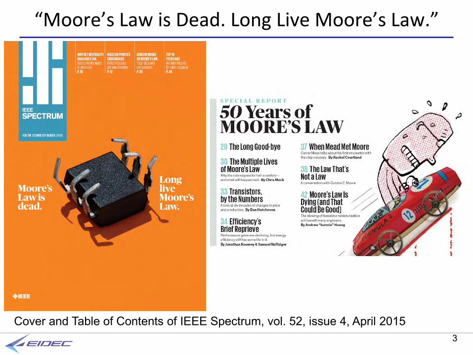
“Moore’s Law is Dead. Long Live Moore’s Law.”
Cover and Table of Contents of IEEE Spectrum, vol. 52, issue 4, April 2015

4
Moore’s Law (G. E. Moore, 1965)“The complexity for minimum component costs has increased at a rate of roughly a factor of two per year”
Ref: Gordon E. Moore, Electronics vol. 38, no. 8, pp. 114-117, 1965
Reprint version: Proc. IEEE vol. 86, no. 1, pp. 82-85, 1998
5
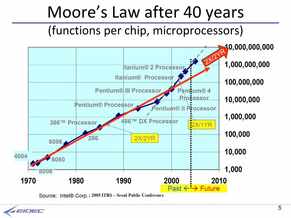
Moore’s Law after 40 years(functions per chip, microprocessors)
6
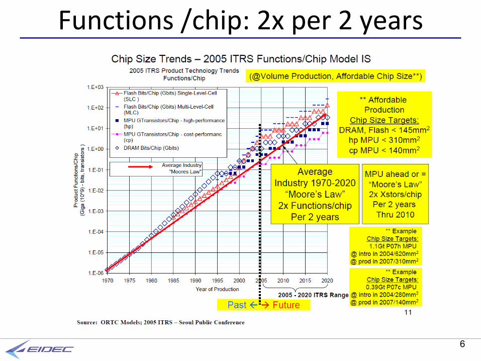
Functions /chip: 2x per 2 years
7
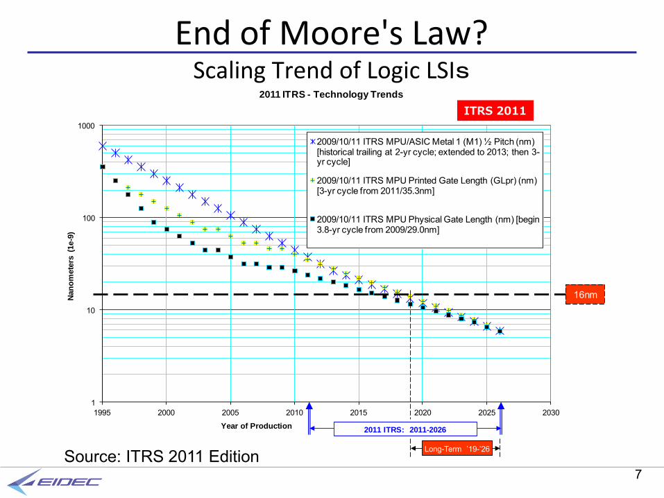
1
10
100
1000
1995 2000 2005 2010 2015 2020 2025 2030
Nan
om
ete
rs (
1e-9
)
Year of Production
2011 ITRS - Technology Trends
2009/10/11 ITRS MPU/ASIC Metal 1 (M1) ½ Pitch (nm) [historical trailing at 2-yr cycle; extended to 2013; then 3-yr cycle]
2009/10/11 ITRS MPU Printed Gate Length (GLpr) (nm) [3-yr cycle from 2011/35.3nm]
2009/10/11 ITRS MPU Physical Gate Length (nm) [begin 3.8-yr cycle from 2009/29.0nm]
2011 ITRS: 2011-2026
Long-Term ’19-’26
16nm
ITRS 2011
End of Moore's Law?Scaling Trend of Logic LSIs
Source: ITRS 2011 Edition

8
1
10
100
1000
1995 2000 2005 2010 2015 2020 2025 2030
Nan
om
ete
rs (
1e-9
)
Year of Production
2011 ITRS - Technology Trends
2009/10/11 ITRS MPU/ASIC Metal 1 (M1) ½ Pitch (nm) [historical trailing at 2-yr cycle; extended to 2013; then 3-yr cycle]
2009/10/11 ITRS MPU Printed Gate Length (GLpr) (nm) [3-yr cycle from 2011/35.3nm]
2009/10/11 ITRS MPU Physical Gate Length (nm) [begin 3.8-yr cycle from 2009/29.0nm]
2011 ITRS: 2011-2026
Long-Term ’19-’26
16nm
Physical Gate Length(High Performance Logic)
Metal1 Half Pitch
ITRS 2015
ITRS 2011 & 2015
“16/14nm”
“11/10nm”“8/7nm”
“6/5nm”
Source: ITRS 2011 Edition / ITRS 2015 Edition
End of Moore‘s Law?Scaling Trend of Logic LSIs
9
10
11
12
13
14

15
16

17
More Complex MOSFET Structure (ITRS 2015)
18

19

20

21
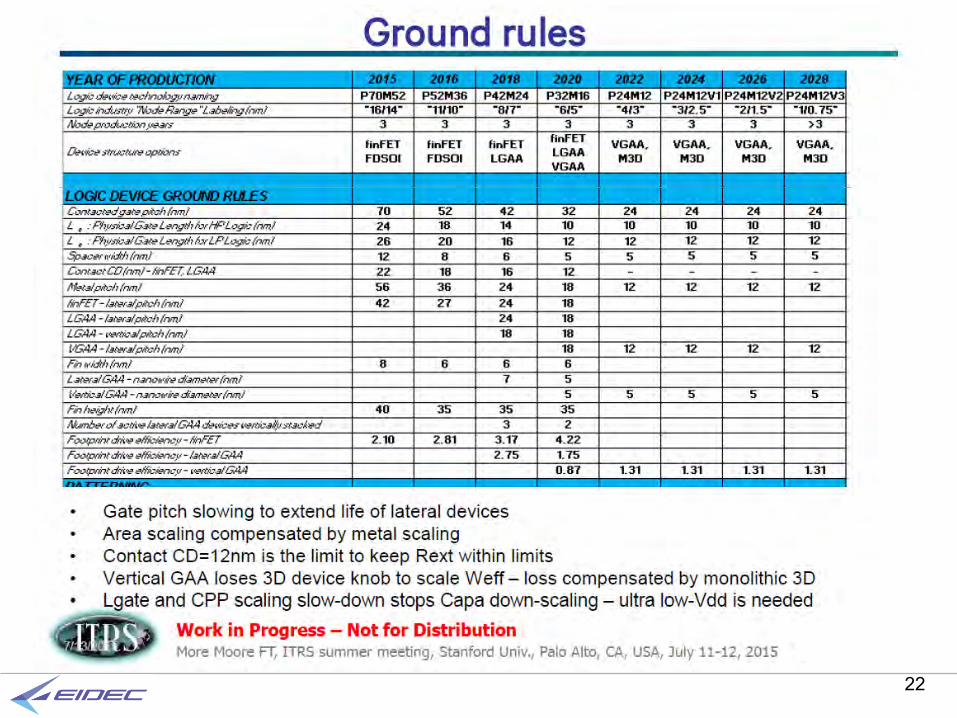
Scaling of MOSFETTable MM01 - More Moore - Logic Core Device Technology Roadmap
YEAR OF PRODUCTION 2015 2017 2019 2021 2024 2027 2030
Logic device technology naming P70M56 P48M36 P42M24 P32M20 P24M12G1 P24M12G2 P24M12G3
Logic industry "Node Range" Labeling (nm) "16/14" "11/10" "8/7" "6/5" "4/3" "3/2.5" "2/1.5"
Logic device structure optionsfinFET
FDSOI
finFET
FDSOI
finFET
LGAA
finFET
LGAA
VGAA
VGAA,
M3DVGAA, M3D VGAA, M3D
LOGIC DEVICE GROUND RULESMPU/SoC Metalx ½ Pitch (nm)[1,2] 28.0 18.0 12.0 10.0 6.0 6.0 6.0
MPU/SoC Metal0/1 ½ Pitch (nm) 28.0 18.0 12.0 10.0 6.0 6.0 6.0
Contacted poly half pitch (nm) 35.0 24.0 21.0 16.0 12.0 12.0 12.0
L g : Physical Gate Length for HP Logic (nm) [3] 24 18 14 10 10 10 10
L g : Physical Gate Length for LP Logic (nm) 26 20 16 12 12 12 12
Gate
FDSOI
TBOX
Gate
FDSOI
TBOX
finFET: fin Field Effect Transistor FDSOI: Fully Depleted Silicon On Wafer
LGAA: Lateral Gate-All-Around VGAA: Vertical Gate-All-Around
M3D: Monolithic 3 Dimensional
Source: ITRS 2015 Edition, “More Moore” Chapter, Table MM01
Table MM01 - More Moore - Logic Core Device Technology Roadmap
YEAR OF PRODUCTION 2015 2017 2019 2021 2024 2027 2030
Logic device technology naming P70M56 P48M36 P42M24 P32M20 P24M12G1 P24M12G2 P24M12G3
Logic industry "Node Range" Labeling (nm) "16/14" "11/10" "8/7" "6/5" "4/3" "3/2.5" "2/1.5"
Logic device structure optionsfinFET
FDSOI
finFET
FDSOI
finFET
LGAA
finFET
LGAA
VGAA
VGAA,
M3DVGAA, M3D VGAA, M3D
LOGIC DEVICE GROUND RULESMPU/SoC Metalx ½ Pitch (nm)[1,2] 28.0 18.0 12.0 10.0 6.0 6.0 6.0
MPU/SoC Metal0/1 ½ Pitch (nm) 28.0 18.0 12.0 10.0 6.0 6.0 6.0
Contacted poly half pitch (nm) 35.0 24.0 21.0 16.0 12.0 12.0 12.0
L g : Physical Gate Length for HP Logic (nm) [3] 24 18 14 10 10 10 10
L g : Physical Gate Length for LP Logic (nm) 26 20 16 12 12 12 12
Gate
FDSOI
TBOX
Gate
FDSOI
TBOX
22

23
3D Cell Arrays of NAND Flash Memories
Floating Gate Cell(intel / Micron)
Charge Trap Cell(Samsung)

24
Rayleigh’s Formula
𝑅 = 𝑘1𝜆
NA
𝑅: Resolution (nm)𝑘1: Constant𝜆: Wave Length (nm)NA:Numerical Aperture
𝑅 (nm) 𝑘1𝜆
(nm)NA
64 0.31193
(ArF)0.93
37 0.26193
(ArF)1.35
12 0.3013.5
(EUV)0.33
7.9 0.3013.5
(EUV)0.51
7.3 0.3013.5
(EUV)0.55
25
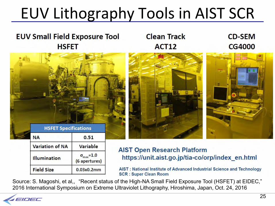
Source: S. Magoshi, et al,, “Recent status of the High-NA Small Field Exposure Tool (HSFET) at EIDEC,” 2016 International Symposium on Extreme Ultraviolet Lithography, Hiroshima, Japan, Oct. 24, 2016
EUV Lithography Tools in AIST SCR

26
Source: S. Magoshi, et al,, “Recent status of the High-NA Small Field Exposure Tool (HSFET) at EIDEC,” 2016 International Symposium on Extreme Ultraviolet Lithography, Hiroshima, Japan, Oct. 24, 2016
Variable NA – NA0.33 vs. NA0.51

27
Source: S. Magoshi, et al,, “Recent status of the High-NA Small Field Exposure Tool (HSFET) at EIDEC,” 2016 International Symposium on Extreme Ultraviolet Lithography, Hiroshima, Japan, Oct. 24, 2016
HSFET Image Contrast (Simulation)

28
Source: S. Magoshi, et al,, “Recent status of the High-NA Small Field Exposure Tool (HSFET) at EIDEC,” 2016 International Symposium on Extreme Ultraviolet Lithography, Hiroshima, Japan, Oct. 24, 2016
Imaging Performance ‐ Quad. Illumination
29
Source: S. Magoshi, et al,, “Recent status of the High-NA Small Field Exposure Tool (HSFET) at EIDEC,” 2016 International Symposium on Extreme Ultraviolet Lithography, Hiroshima, Japan, Oct. 24, 2016
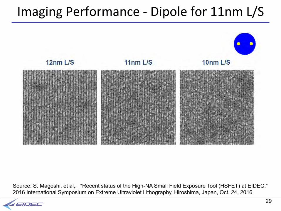
Imaging Performance ‐ Dipole for 11nm L/S
30
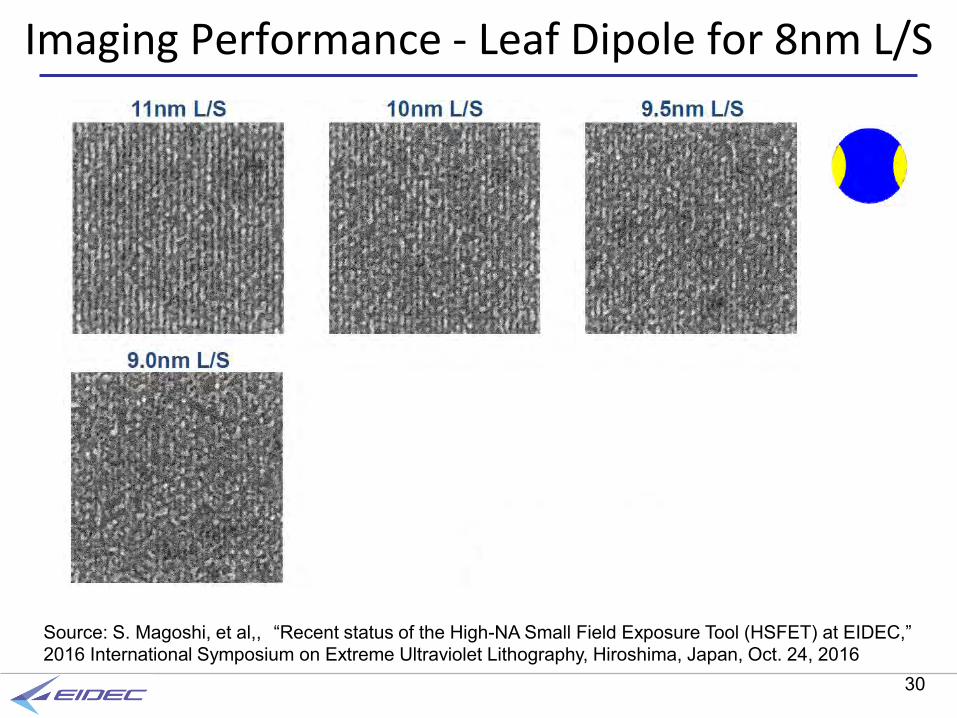
Source: S. Magoshi, et al,, “Recent status of the High-NA Small Field Exposure Tool (HSFET) at EIDEC,” 2016 International Symposium on Extreme Ultraviolet Lithography, Hiroshima, Japan, Oct. 24, 2016
Imaging Performance ‐ Leaf Dipole for 8nm L/S
31
32
33
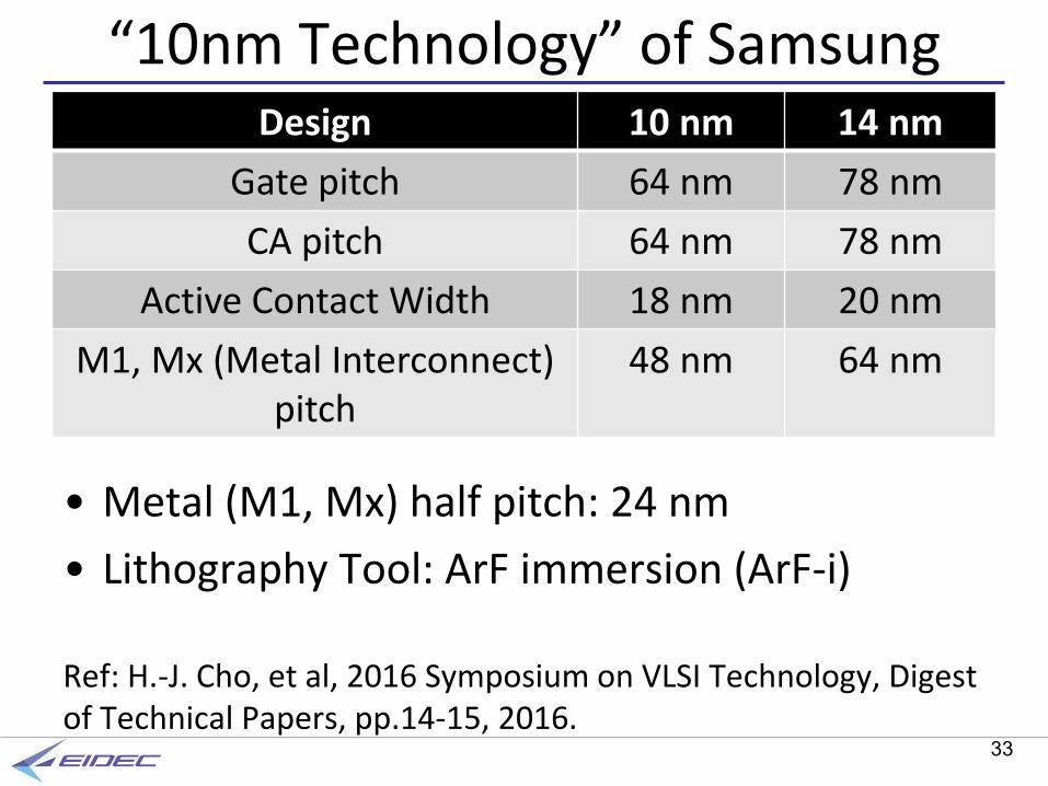
“10nm Technology” of SamsungDesign 10 nm 14 nm
Gate pitch 64 nm 78 nm
CA pitch 64 nm 78 nm
Active Contact Width 18 nm 20 nm
M1, Mx (Metal Interconnect) pitch
48 nm 64 nm
• Metal (M1, Mx) half pitch: 24 nm
• Lithography Tool: ArF immersion (ArF-i)
Ref: H.-J. Cho, et al, 2016 Symposium on VLSI Technology, Digest of Technical Papers, pp.14-15, 2016.
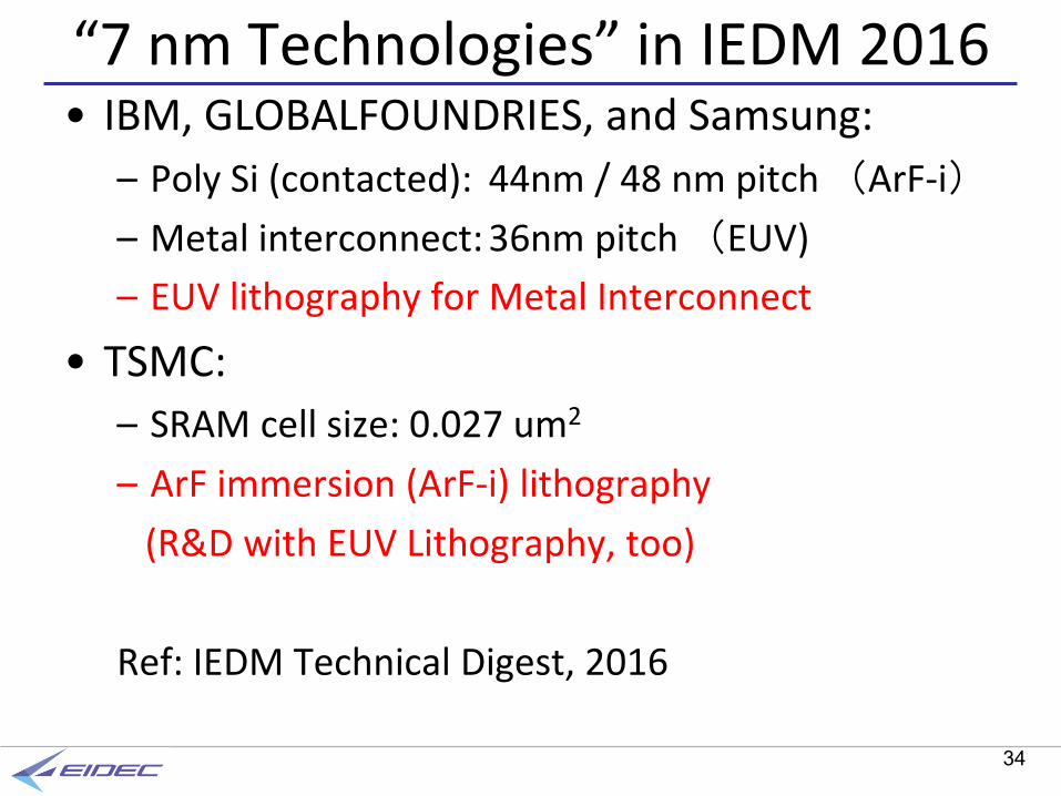
34
“7 nm Technologies” in IEDM 2016• IBM, GLOBALFOUNDRIES, and Samsung:
– Poly Si (contacted): 44nm / 48 nm pitch (ArF-i)
– Metal interconnect: 36nm pitch (EUV)
– EUV lithography for Metal Interconnect
• TSMC:
– SRAM cell size: 0.027 um2
– ArF immersion (ArF-i) lithography
(R&D with EUV Lithography, too)
Ref: IEDM Technical Digest, 2016

35
IEDM 2016, #2.6, IBM/GF/Samsung
Ref: IEDM Technical Digest, 2016

36
IEDM 2016, #2.6, IBM/GF/Samsung
Ref: IEDM Technical Digest, 2016
37
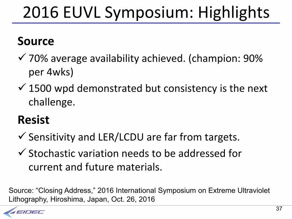
2016 EUVL Symposium: Highlights
Source
70% average availability achieved. (champion: 90% per 4wks)
1500 wpd demonstrated but consistency is the next challenge.
Resist
Sensitivity and LER/LCDU are far from targets.
Stochastic variation needs to be addressed for current and future materials.
Source: “Closing Address,” 2016 International Symposium on Extreme Ultraviolet Lithography, Hiroshima, Japan, Oct. 26, 2016

38
2016 EUVL Symposium: HighlightsMask
Very positive year (ABI optic upgraded, AIMS tool shipped).
Blank suppliers making progress (0 defect blanks possible).
Infrastructure gap for pattern mask inspection.
Pellicle (keeping mask clean)
Good progress but very far to go for HVM readiness.
Need industry focus to bring all the required components together.
Source: “Closing Address,” 2016 International Symposium on Extreme Ultraviolet Lithography, Hiroshima, Japan, Oct. 26, 2016

39
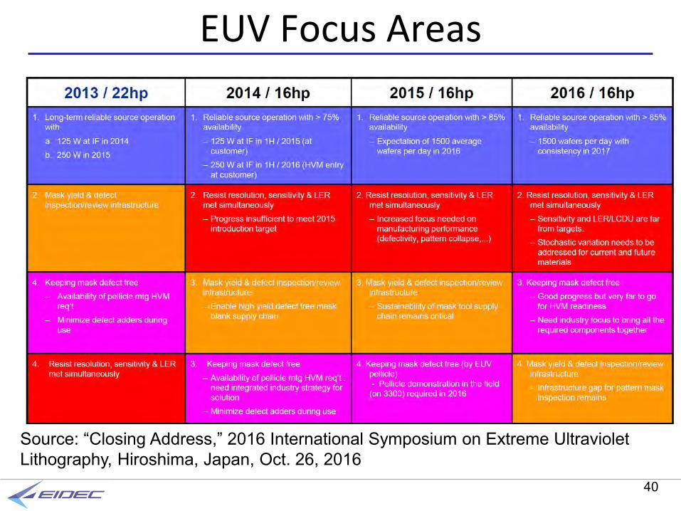
2016 EUV Focus Areas
Source: “Closing Address,” 2016 International Symposium on Extreme Ultraviolet Lithography, Hiroshima, Japan, Oct. 26, 2016
40
EUV Focus Areas
Source: “Closing Address,” 2016 International Symposium on Extreme Ultraviolet Lithography, Hiroshima, Japan, Oct. 26, 2016

41
EUV-FEL (Free Electron Laser)
Source: H. Kawata, “Strategy to realize the EUV-FEL high power light source,” 2016 International Symposium on Extreme Ultraviolet Lithography, Hiroshima, Japan, Oct. 24, 2016

42
Potential Problems in EUV-FEL• R&D expense to develop EUV-FEL
– Who pays the cost? International collaboration necessary.
– When and where available?
• Cost of ownership
– to be less expensive than existing EUV source
• Foot print
• Stable operation
– two beam lines are necessary for back up
• Generation of radioactive materials due to high energy electron irradiation
• High peak power
– potential damage in mirrors and reticles
– Resist
• Too coherent EUV light

43
Tradeoff: Resolution vs Sensitivity
Low sensitivity is acceptable if higher EUV source power is available.
Ref: 2016 International Symposium on Extreme Ultraviolet Lithography, Hiroshima, Japan
44
Summary
• Scaling limit is 10nm for MOSFET gate length; 6nm for metal interconnect, according to ITRS 2015.
• Performance and degree of integration will be getting better by using new device structures, new materials, 3D device structure, 3D assembly & packaging, etc. even if we reach the scaling limit
• EUV lithography will be used in mass production tool for 7nm or 5nm logic products and beyond.
• EUV-FEL is a possible solution as an EUV source with higher average power than 1 kW. Its cost of ownership, peak power, coherence of the EUV-FEL source might be the potential problems to be solved
45
• ITRS (International Technology Roadmap for Semiconductors)– http://www.itrs2.net/– ITRS latest version, and archives– White Paper, Presentation Materials, etc.
• JEITA / STRJ (Semiconductor Technology Roadmap committee of Japan)– http://semicon.jeita.or.jp/STRJ/– ITRS 2013 Edition (Japanese version) and older– Presentation material of STRJ Workshop, etc.
• SEMATECH and ISMI Proceedings Archives: Lithography– http://www.sematech.org/meetings/archives/litho/index.htm
• IEUVI (International EUV Initiative)– http://ieuvi.org/index.html– http://ieuvi.org/TWG/IEUVI_TWGs01.htm
References


![ITRS Winter Conference 2007 Makuhara, Japan 1 International Technology Roadmap for Semiconductors 2007 ITRS ORTC [12/5 Makuhari Japan ITRS Public Conference]](https://img.dokumen.tips/doc/110x75/5514961d550346b0158b62f5/itrs-winter-conference-2007-makuhara-japan-1-international-technology-roadmap-for-semiconductors-2007-itrs-ortc-125-makuhari-japan-itrs-public-conference.jpg)