Embed Size (px)
Citation preview
Rev. 2.0
Seiko Instruments Inc. 1
SUPER-SMALL PACKAGE HIGH-PRECISION VOLTAGE DETECTOR S-808 Series
The S-808 Series is a high-precision voltage detector developed usingCMOS process. The detection voltage is fixed internally, with anaccuracy of ±2.0%. Two output types, Nch open-drain and CMOSoutput, are available.
n Features
ùUltra-low current consumption
1.3 µA typ. (VDD=1.5 V)
Products with detection voltage of 1.4 V or lesselectronic
0.8µA typ. (VDD=3.5 V)
Products with detection voltage of 1.5 V or more
ùHigh-precision detection voltage
±2.0%
ùLow operating voltage
0.7 to 5.0 V
Products with detection voltage of 1.4 V or less
0.95 to 10.0 V
Products with a detection voltage of 1.5 V or more
ùHysteresis characteristics
5% typ.
ùDetection voltage
0.8 to 6.0 V
(0.1 V step)
ùNch open-drain active low and CMOS active low output
ùSC-82AB Super-small plastic package
ùTO-92 Plastic package
ùSOT-89-3 Miniaturized power mold plastic package
ùSOT-23-5 Very-small plastic package
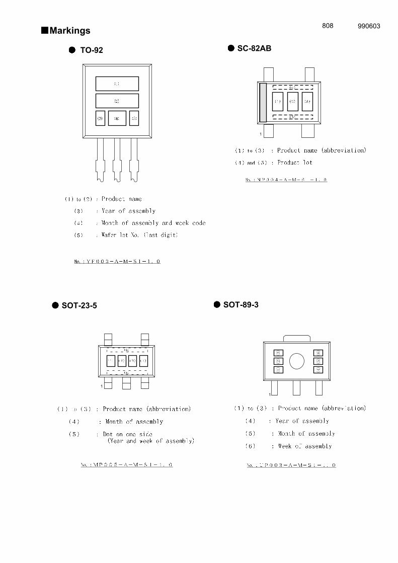
n Pin Assignment
(1) SC-82AB (2) TO-92 (3) SOT-89-3 (4) SOT-23-5
n Applications
ùBattery checker
ùPower failure detector
ùPower monitor for pagers, calculators,organizers,
ùConstant voltage power monitor for cameras,
video equipment, communication devices
ùPower monitor for microcomputers and resetCPUs
Top view
1 2 3
1 2 3 Bottom view
1 OUT2 VDD
3 VSS
Top view5 4
321
1 OUT2 VDD
3 NC4 VSS
4 3
21
1 OUT2 VDD
3 VSS
1 OUT2 VDD
3 VSS
4 NC5 NC
Figure 1
Top view
SUPER-SMALL PACKAGE HIGH-PRECISION VOLTAGE DETECTORS-808 Series
2 Seiko Instruments Inc.
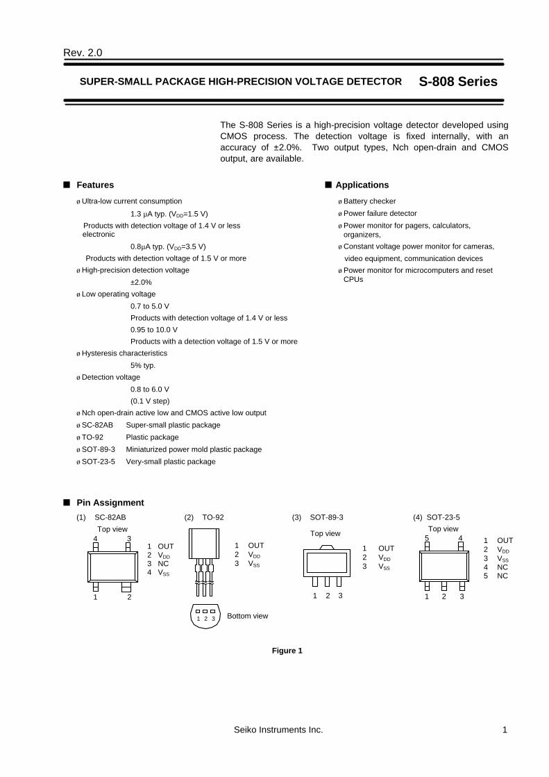
n Block Diagram
(1) Nch open-drain active low output (2) CMOS active low output
OUT
VREF
VSS
−
+
VDD
*
OUT
VREF
VSS
VDD
*
*
−
+
*Parasitic diode
Figure 2
n Selection Guide
S-808XX AX XX - XXX - T2
Output typeN: Nch open-drain (active low output)L: CMOS (active low output)
Detection voltage rank
Package name (abbreviation)NP: SC-82ABMP: SOT-23-5UP: SOT-89-3Y: TO-92
Product name (abbreviation)Directions of the IC for taping specifications
SUPER-SMALL PACKAGE HIGH-PRECISION VOLTAGE DETECTOR S-808 Series
Seiko Instruments Inc. 3
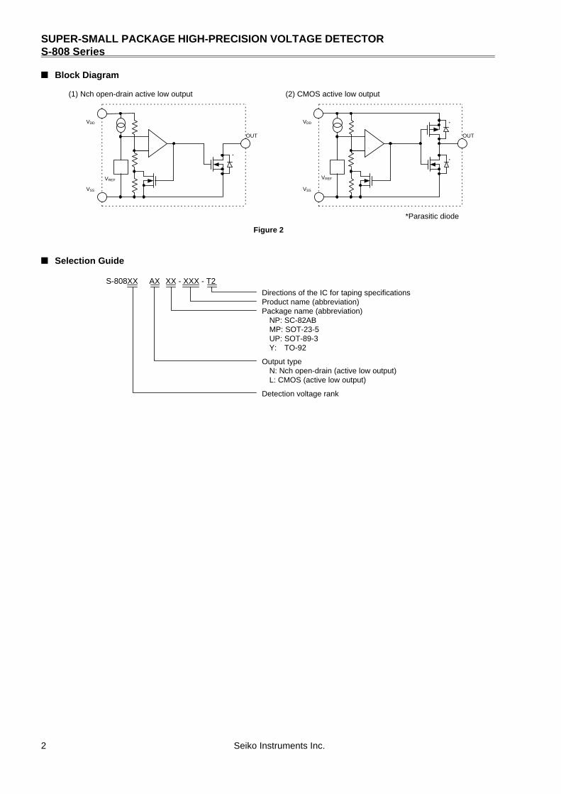
Table 1
Detection voltage range Hysteresis width Nch Open Drain(Low)(V) VHYS typ.(V) SC-82AB TO-92 SOT-89-3 SOT-23-5
0.8V±2.0% 0.034 S-80808ANNP-E7Y-T2 — — —
0.9V±2.0% 0.044 S-80809ANNP-E7Z-T2 — — —
1.0V±2.0% 0.054 S-80810ANNP-E70-T2 — — —
1.1V±2.0% 0.064 S-80811ANNP-E71-T2 — — —
1.2V±2.0% 0.073 S-80812ANNP-E72-T2 — — —
1.3V±2.0% 0.083 S-80813ANNP-EDA-T2 — — —
1.4V±2.0% 0.093 S-80814ANNP-EDB-T2 — — —
1.5V±2.0% 0.075 S-80815ANNP-EDC-T2 S-80815ANY S-80815ANUP-EDC-T2 —
1.6V±2.0% 0.080 S-80816ANNP-EDD-T2 S-80816ANY S-80816ANUP-EDD-T2 —
1.7V±2.0% 0.085 S-80817ANNP-EDE-T2 S-80817ANY S-80817ANUP-EDE-T2 S-80817ANMP-EDE-T2
1.8V±2.0% 0.090 S-80818ANNP-EDF-T2 S-80818ANY S-80818ANUP-EDF-T2 S-80818ANMP-EDF-T2
1.9V±2.0% 0.095 S-80819ANNP-EDG-T2 S-80819ANY S-80819ANUP-EDG-T2 S-80819ANMP-EDG-T2
2.0V±2.0% 0.100 S-80820ANNP-EDH-T2 S-80820ANY S-80820ANUP-EDH-T2 S-80820ANMP-EDH-T2
2.1V±2.0% 0.105 S-80821ANNP-EDJ-T2 S-80821ANY S-80821ANUP-EDJ-T2 S-80821ANMP-EDJ-T2
2.2V±2.0% 0.110 S-80822ANNP-EDK-T2 S-80822ANY S-80822ANUP-EDK-T2 S-80822ANMP-EDK-T2
2.3V±2.0% 0.115 S-80823ANNP-EDL-T2 S-80823ANY S-80823ANUP-EDL-T2 S-80823ANMP-EDL-T2
2.4V±2.0% 0.120 S-80824ANNP-EDM-T2 S-80824ANY S-80824ANUP-EDM-T2 S-80824ANMP-EDM-T2
2.5V±2.0% 0.125 S-80825ANNP-EDN-T2 S-80825ANY S-80825ANUP-EDN-T2 S-80825ANMP-EDN-T2
2.6V±2.0% 0.130 S-80826ANNP-EDP-T2 S-80826ANY S-80826ANUP-EDP-T2 —
2.7V±2.0% 0.135 S-80827ANNP-EDQ-T2 S-80827ANY S-80827ANUP-EDQ-T2 S-80827ANMP-EDQ-T2
2.8V±2.0% 0.140 S-80828ANNP-EDR-T2 S-80828ANY S-80828ANUP-EDR-T2 S-80828ANMP-EDR-T2
2.9V±2.0% 0.145 S-80829ANNP-EDS-T2 S-80829ANY S-80829ANUP-EDS-T2 —
3.0V±2.0% 0.150 S-80830ANNP-EDT-T2 S-80830ANY S-80830ANUP-EDT-T2 S-80830ANMP-EDT-T2
3.1V±2.0% 0.155 S-80831ANNP-EDV-T2 S-80831ANY S-80831ANUP-EDV-T2 —
3.2V±2.0% 0.160 S-80832ANNP-EDW-T2 S-80832ANY S-80832ANUP-EDW-T2 S-80832ANMP-EDW-T2
3.3V±2.0% 0.165 S-80833ANNP-EDX-T2 S-80833ANY S-80833ANUP-EDX-T2 S-80833ANMP-EDX-T2
3.4V±2.0% 0.170 S-80834ANNP-EDY-T2 S-80834ANY S-80834ANUP-EDY-T2 S-80834ANMP-EDY-T2
3.5V±2.0% 0.175 S-80835ANNP-EDZ-T2 S-80835ANY S-80835ANUP-EDZ-T2 S-80835ANMP-EDZ-T2
3.6V±2.0% 0.180 S-80836ANNP-ED0-T2 S-80836ANY S-80836ANUP-ED0-T2 S-80836ANMP-ED0-T2
3.7V±2.0% 0.185 S-80837ANNP-ED1-T2 S-80837ANY S-80837ANUP-ED1-T2 —
3.8V±2.0% 0.190 S-80838ANNP-ED2-T2 S-80838ANY S-80838ANUP-ED2-T2 —
3.9V±2.0% 0.195 S-80839ANNP-ED3-T2 S-80839ANY S-80839ANUP-ED3-T2 S-80839ANMP-ED3-T2
4.0V±2.0% 0.200 S-80840ANNP-ED4-T2 S-80840ANY S-80840ANUP-ED4-T2 S-80840ANMP-ED4-T2
4.1V±2.0% 0.205 S-80841ANNP-ED5-T2 S-80841ANY S-80841ANUP-ED5-T2 —
4.2V±2.0% 0.210 S-80842ANNP-ED6-T2 S-80842ANY S-80842ANUP-ED6-T2 S-80842ANMP-ED6-T2
4.3V±2.0% 0.215 S-80843ANNP-ED7-T2 S-80843ANY S-80843ANUP-ED7-T2 —
4.4V±2.0% 0.220 S-80844ANNP-ED8-T2 S-80844ANY S-80844ANUP-ED8-T2 S-80844ANMP-ED8-T2
4.5V±2.0% 0.225 S-80845ANNP-ED9-T2 S-80845ANY S-80845ANUP-ED9-T2 S-80845ANMP-ED9-T2
4.6V±2.0% 0.230 S-80846ANNP-EJA-T2 S-80846ANY S-80846ANUP-EJA-T2 —
4.7V±2.0% 0.235 S-80847ANNP-EJB-T2 S-80847ANY S-80847ANUP-EJB-T2 —
4.8V±2.0% 0.240 S-80848ANNP-EJC-T2 S-80848ANY S-80848ANUP-EJC-T2 —
4.9V±2.0% 0.245 S-80849ANNP-EJD-T2 S-80849ANY S-80849ANUP-EJD-T2 —
5.0V±2.0% 0.250 S-80850ANNP-EJE-T2 S-80850ANY S-80850ANUP-EJE-T2 S-80850ANMP-EJE-T2
5.1V±2.0% 0.255 S-80851ANNP-EJF-T2 S-80851ANY S-80851ANUP-EJF-T2 S-80851ANMP-EJF-T2
5.2V±2.0% 0.260 S-80852ANNP-EJG-T2 — S-80852ANUP-EJG-T2 —
5.3V±2.0% 0.265 S-80853ANNP-EJH-T2 S-80853ANY — —
5.4V±2.0% 0.270 S-80854ANNP-EJJ-T2 — — —
5.5V±2.0% 0.275 S-80855ANNP-EJK-T2 — — —
5.6V±2.0% 0.280 S-80856ANNP-EJL-T2 — — —
5.7V±2.0% 0.285 S-80857ANNP-EJM-T2 — — —
5.8V±2.0% 0.290 S-80858ANNP-EJN-T2 — — —
5.9V±2.0% 0.295 S-80859ANNP-EJP-T2 — — —
6.0V±2.0% 0.300 S-80860ANNP-EJQ-T2 — S-80860ANUP-EJQ-T2 —
SUPER-SMALL PACKAGE HIGH-PRECISION VOLTAGE DETECTORS-808 Series
4 Seiko Instruments Inc.
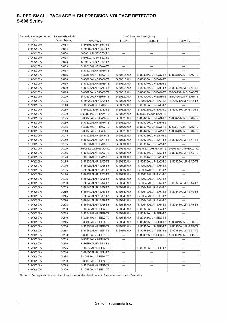
Detection voltage range Hysteresis width CMOS Output Drain(Low)(V) VHYS typ.(V) SC-82AB TO-92 SOT-89-3 SOT-23-5
0.8V±2.0% 0.034 S-80808ALNP-E5Y-T2 — — —
0.9V±2.0% 0.044 S-80809ALNP-E5Z-T2 — — —
1.0V±2.0% 0.054 S-80810ALNP-E50-T2 — — —
1.1V±2.0% 0.064 S-80811ALNP-E51-T2 — — —
1.2V±2.0% 0.073 S-80812ALNP-E52-T2 — — —
1.3V±2.0% 0.083 S-80813ALNP-EAA-T2 — — —
1.4V±2.0% 0.093 S-80814ALNP-EAB-T2 — — —
1.5V±2.0% 0.075 S-80815ALNP-EAC-T2 S-80815ALY S-80815ALUP-EAC-T2 S-80815ALMP-EAC-T2
1.6V±2.0% 0.080 S-80816ALNP-EAD-T2 S-80816ALY S-80816ALUP-EAD-T2 —
1.7V±2.0% 0.085 S-80817ALNP-EAE-T2 S-80817ALY S-80817ALUP-EAE-T2 —
1.8V±2.0% 0.090 S-80818ALNP-EAF-T2 S-80818ALY S-80818ALUP-EAF-T2 S-80818ALMP-EAF-T2
1.9V±2.0% 0.095 S-80819ALNP-EAG-T2 S-80819ALY S-80819ALUP-EAG-T2 S-80819ALMP-EAG-T2
2.0V±2.0% 0.100 S-80820ALNP-EAH-T2 S-80820ALY S-80820ALUP-EAH-T2 S-80820ALMP-EAH-T2
2.1V±2.0% 0.105 S-80821ALNP-EAJ-T2 S-80821ALY S-80821ALUP-EAJ-T2 S-80821ALMP-EAJ-T2
2.2V±2.0% 0.110 S-80822ALNP-EAK-T2 S-80822ALY S-80822ALUP-EAK-T2 —
2.3V±2.0% 0.115 S-80823ALNP-EAL-T2 S-80823ALY S-80823ALUP-EAL-T2 S-80823ALMP-EAL-T2
2.4V±2.0% 0.120 S-80824ALNP-EAM-T2 S-80824ALY S-80824ALUP-EAM-T2 —
2.5V±2.0% 0.125 S-80825ALNP-EAN-T2 S-80825ALY S-80825ALUP-EAN-T2 S-80825ALMP-EAN-T2
2.6V±2.0% 0.130 S-80826ALNP-EAP-T2 S-80826ALY S-80826ALUP-EAP-T2 —
2.7V±2.0% 0.135 S-80827ALNP-EAQ-T2 S-80827ALY S-80827ALUP-EAQ-T2 S-80827ALMP-EAQ-T2
2.8V±2.0% 0.140 S-80828ALNP-EAR-T2 S-80828ALY S-80828ALUP-EAR-T2 S-80828ALMP-EAR-T2
2.9V±2.0% 0.145 S-80829ALNP-EAS-T2 S-80829ALY S-80829ALUP-EAS-T2 —
3.0V±2.0% 0.150 S-80830ALNP-EAT-T2 S-80830ALY S-80830ALUP-EAT-T2 S-80830ALMP-EAT-T2
3.1V±2.0% 0.155 S-80831ALNP-EAV-T2 S-80831ALY S-80831ALUP-EAV-T2 —
3.2V±2.0% 0.160 S-80832ALNP-EAW-T2 S-80832ALY S-80832ALUP-EAW-T2 S-80832ALMP-EAW-T2
3.3V±2.0% 0.165 S-80833ALNP-EAX-T2 S-80833ALY S-80833ALUP-EAX-T2 S-80833ALMP-EAX-T2
3.4V±2.0% 0.170 S-80834ALNP-EAY-T2 S-80834ALY S-80834ALUP-EAY-T2 —
3.5V±2.0% 0.175 S-80835ALNP-EAZ-T2 S-80835ALY S-80835ALUP-EAZ-T2 S-80835ALMP-EAZ-T2
3.6V±2.0% 0.180 S-80836ALNP-EA0-T2 S-80836ALY S-80836ALUP-EA0-T2 —
3.7V±2.0% 0.185 S-80837ALNP-EA1-T2 S-80837ALY S-80837ALUP-EA1-T2 —
3.8V±2.0% 0.190 S-80838ALNP-EA2-T2 S-80838ALY S-80838ALUP-EA2-T2 —
3.9V±2.0% 0.195 S-80839ALNP-EA3-T2 S-80839ALY S-80839ALUP-EA3-T2 —
4.0V±2.0% 0.200 S-80840ALNP-EA4-T2 S-80840ALY S-80840ALUP-EA4-T2 S-80840ALMP-EA4-T2
4.1V±2.0% 0.205 S-80841ALNP-EA5-T2 S-80841ALY S-80841ALUP-EA5-T2 —
4.2V±2.0% 0.210 S-80842ALNP-EA6-T2 S-80842ALY S-80842ALUP-EA6-T2 S-80842ALMP-EA6-T2
4.3V±2.0% 0.215 S-80843ALNP-EA7-T2 S-80843ALY S-80843ALUP-EA7-T2 —
4.4V±2.0% 0.220 S-80844ALNP-EA8-T2 S-80844ALY S-80844ALUP-EA8-T2 —
4.5V±2.0% 0.225 S-80845ALNP-EA9-T2 S-80845ALY S-80845ALUP-EA9-T2 S-80845ALMP-EA9-T2
4.6V±2.0% 0.230 S-80846ALNP-EEA-T2 S-80846ALY S-80846ALUP-EEA-T2 —
4.7V±2.0% 0.235 S-80847ALNP-EEB-T2 S-80847ALY S-80847ALUP-EEB-T2 —
4.8V±2.0% 0.240 S-80848ALNP-EEC-T2 S-80848ALY S-80848ALUP-EEC-T2 —
4.9V±2.0% 0.245 S-80849ALNP-EED-T2 S-80849ALY S-80849ALUP-EED-T2 S-80849ALMP-EED-T2
5.0V±2.0% 0.250 S-80850ALNP-EEE-T2 S-80850ALY S-80850ALUP-EEE-T2 S-80850ALMP-EEE-T2
5.1V±2.0% 0.255 S-80851ALNP-EEF-T2 S-80851ALY S-80851ALUP-EEF-T2 S-80851ALMP-EEF-T2
5.2V±2.0% 0.260 S-80852ALNP-EEG-T2 — S-80852ALUP-EEG-T2 S-80852ALMP-EEG-T2
5.3V±2.0% 0.265 S-80853ALNP-EEH-T2 — — —
5.4V±2.0% 0.270 S-80854ALNP-EEJ-T2 — — —
5.5V±2.0% 0.275 S-80855ALNP-EEK-T2 — S-80855ALUP-EEK-T2 —
5.6V±2.0% 0.280 S-80856ALNP-EEL-T2 — — —
5.7V±2.0% 0.285 S-80857ALNP-EEM-T2 — — —
5.8V±2.0% 0.290 S-80858ALNP-EEN-T2 — — —
5.9V±2.0% 0.295 S-80859ALNP-EEP-T2 — — —
6.0V±2.0% 0.300 S-80860ALNP-EEQ-T2 — — —
Remark: Some products described here in are under development. Please contact us for Samples.
SUPER-SMALL PACKAGE HIGH-PRECISION VOLTAGE DETECTOR S-808 Series
Seiko Instruments Inc. 5
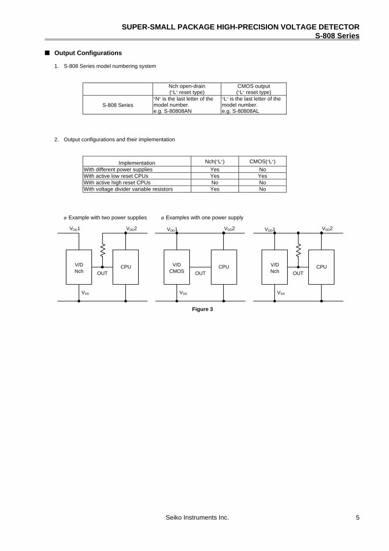
n Output Configurations
1. S-808 Series model numbering system
Nch open-drain(“L” reset type)
CMOS output(“L” reset type)
S-808 Series“N” is the last letter of themodel number.e.g. S-80808AN
“L” is the last letter of themodel number.e.g. S-80808AL
2. Output configurations and their implementation
Implementation Nch(“L”) CMOS(“L”)
With different power supplies Yes NoWith active low reset CPUs Yes YesWith active high reset CPUs No NoWith voltage divider variable resistors Yes No
ù Example with two power supplies ù Examples with one power supply
VSS
OUTCPU
VDD2VDD1
V/DNch
VSS
OUTCPU
VDD2VDD1
V/DCMOS
VSS
OUTCPU
VDD2VDD1
V/DNch
Figure 3
SUPER-SMALL PACKAGE HIGH-PRECISION VOLTAGE DETECTORS-808 Series
6 Seiko Instruments Inc.
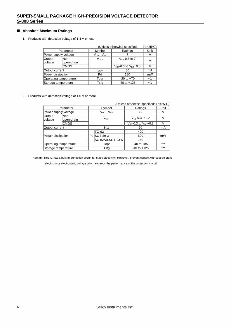
n Absolute Maximum Ratings
1. Products with detection voltage of 1.4 V or less
(Unless otherwise specified: Ta=25°C)Parameter Symbol Ratings Unit
Power supply voltage VDD - VSS 7 VOutputvoltage
Nchopen-drain
VOUT VSS-0.3 to 7V
CMOS VSS-0.3 to VDD+0.3 VOutput current IOUT 50 mAPower dissipation Pd 150 mWOperating temperature Topr -20 to +70 °CStorage temperature Tstg -40 to +125 °C
2. Products with detection voltage of 1.5 V or more
(Unless otherwise specified: Ta=25°C)Parameter Symbol Ratings Unit
Power supply voltage VDD - VSS 12 VOutputvoltage
Nchopen-drain VOUT VSS-0.3 to 12 V
CMOS VSS-0.3 to VDD+0.3 VOutput current IOUT 50 mA
TO-92 400Power dissipation Pd SOT-89-3 500 mW
SC-82AB,SOT-23-5 150Operating temperature Topr -40 to +85 °CStorage temperature Tstg -40 to +125 °C
Remark:This IC has a built-in protection circuit for static electricity. However, prevent contact with a large static
electricity or electrostatic voltage which exceeds the performance of the protection circuit
SUPER-SMALL PACKAGE HIGH-PRECISION VOLTAGE DETECTOR S-808 Series
Seiko Instruments Inc. 7
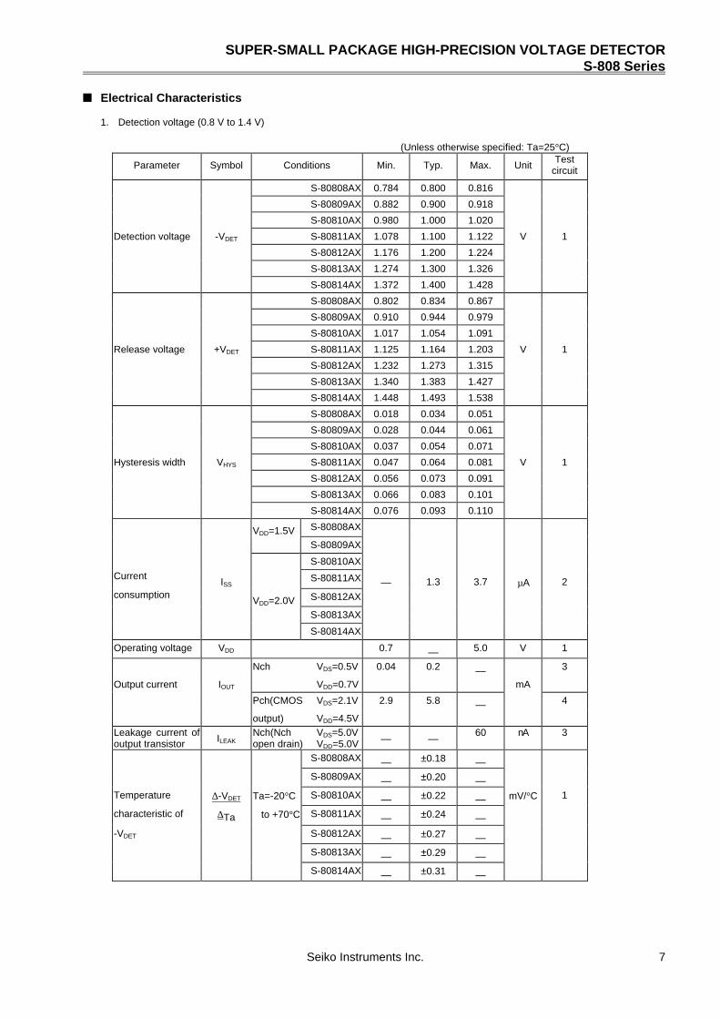
n Electrical Characteristics
1. Detection voltage (0.8 V to 1.4 V)
(Unless otherwise specified: Ta=25°C)
Parameter Symbol Conditions Min. Typ. Max. UnitTest
circuit
S-80808AX 0.784 0.800 0.816
S-80809AX 0.882 0.900 0.918
S-80810AX 0.980 1.000 1.020
Detection voltage -VDET S-80811AX 1.078 1.100 1.122 V 1
S-80812AX 1.176 1.200 1.224
S-80813AX 1.274 1.300 1.326
S-80814AX 1.372 1.400 1.428
S-80808AX 0.802 0.834 0.867
S-80809AX 0.910 0.944 0.979
S-80810AX 1.017 1.054 1.091
Release voltage +VDET S-80811AX 1.125 1.164 1.203 V 1
S-80812AX 1.232 1.273 1.315
S-80813AX 1.340 1.383 1.427
S-80814AX 1.448 1.493 1.538
S-80808AX 0.018 0.034 0.051
S-80809AX 0.028 0.044 0.061
S-80810AX 0.037 0.054 0.071
Hysteresis width VHYS S-80811AX 0.047 0.064 0.081 V 1
S-80812AX 0.056 0.073 0.091
S-80813AX 0.066 0.083 0.101
S-80814AX 0.076 0.093 0.110
VDD=1.5V S-80808AX
S-80809AX
S-80810AX
CurrentISS
S-80811AX — 1.3 3.7 µA 2consumption
VDD=2.0V S-80812AX
S-80813AX
S-80814AX
Operating voltage VDD 0.7 — 5.0 V 1
Nch VDS=0.5V 0.04 0.2 — 3
Output current IOUT VDD=0.7V mA
Pch(CMOS VDS=2.1V 2.9 5.8 — 4
output) VDD=4.5VLeakage current ofoutput transistor ILEAK
Nch(Nchopen drain)
VDS=5.0VVDD=5.0V — —
60 nA 3
S-80808AX — ±0.18 —S-80809AX — ±0.20 —
Temperature ∆-VDET Ta=-20°C S-80810AX — ±0.22 — mV/°C 1
characteristic of ∆Ta to +70°C S-80811AX — ±0.24 —
-VDET S-80812AX — ±0.27 —S-80813AX — ±0.29 —S-80814AX — ±0.31 —
SUPER-SMALL PACKAGE HIGH-PRECISION VOLTAGE DETECTORS-808 Series
8 Seiko Instruments Inc.
2. Detection voltage (1.5 V to 2.6 V)
(Unless otherwise specified: Ta=25°C)
Parameter Symbol Conditions Min. Typ. Max. UnitTest
circuit
S-80815AX 1.470 1.500 1.530
S-80816AX 1.568 1.600 1.632
S-80817AX 1.666 1.700 1.734
S-80818AX 1.764 1.800 1.836
S-80819AX 1.862 1.900 1.938
Detection voltage -VDET S-80820AX 1.960 2.000 2.040 V 1
S-80821AX 2.058 2.100 2.142
S-80822AX 2.156 2.200 2.244
S-80823AX 2.254 2.300 2.346
S-80824AX 2.352 2.400 2.448
S-80825AX 2.450 2.500 2.550
S-80826AX 2.548 2.600 2.652
Hysteresis width VHYS-VDET
×0.03-VDET
×0.05-VDET
×0.08V 1
Currentconsumption ISS VDD=3.5V — 0.8 2.4 µA 2
Operating voltage VDD 0.95 — 10.0 V 1
Nch VDD=1.2V 0.23 0.50 — 3
Output current VDS=0.5V
IOUT Pch(CMOS mA
output) VDD=4.8V 0.36 0.62 — 4
VDS=0.5VLeakage current ofoutput transistor ILEAK
Nch(Nchopen drain)
VDS=10.0VVDD=10.0V
— —0.1 µA 3
Response time tPLH — — 60 µs 1
S-80815AX — ±0.18 ±0.54
S-80816AX — ±0.19 ±0.57
S-80817AX — ±0.20 ±0.60
S-80818AX — ±0.21 ±0.63
Temperature S-80819AX — ±0.22 ±0.66
characteristic of ∆-VDET Ta=-40°C S-80820AX — ±0.24 ±0.72 mV/°C 1
-VDET ∆Ta to +85°C S-80821AX — ±0.25 ±0.75
S-80822AX — ±0.26 ±0.78
S-80823AX — ±0.27 ±0.81
S-80824AX — ±0.28 ±0.84
S-80825AX — ±0.29 ±0.87
S-80826AX — ±0.31 ±0.93
SUPER-SMALL PACKAGE HIGH-PRECISION VOLTAGE DETECTOR S-808 Series
Seiko Instruments Inc. 9
3. Detection voltage (2.7 V to 3.9 V)
(Unless otherwise specified: Ta=25°C)
Parameter Symbol Conditions Min. Typ. Max. UnitTest
circuit
S-80827AX 2.646 2.700 2.754
S-80828AX 2.744 2.800 2.856
S-80829AX 2.842 2.900 2.958
S-80830AX 2.940 3.000 3.060
S-80831AX 3.038 3.100 3.162
S-80832AX 3.136 3.200 3.264
Detection voltage -VDET S-80833AX 3.234 3.300 3.366 V 1
S-80834AX 3.332 3.400 3.468
S-80835AX 3.430 3.500 3.570
S-80836AX 3.528 3.600 3.672
S-80837AX 3.626 3.700 3.774
S-80838AX 3.724 3.800 3.876
S-80839AX 3.822 3.900 3.978
Hysteresis width VHYS-VDET
×0.03-VDET
×0.05-VDET
×0.08V 1
Currentconsumption ISS VDD=4.5V — 0.9 2.7 µA 2
Operating voltage VDD 0.95 — 10.0 V 1
Nch VDD=1.2V 0.23 0.50 —Output current VDS=0.5V VDD=2.4V 1.60 3.70 — 3
IOUT Pch(CMOS mA
output) VDD=4.8V 0.36 0.62 — 4
VDS=0.5VLeakage current ofoutput transistor ILEAK
Nch(Nchopen drain)
VDS=10.0VVDD=10.0V
— — 0.1 µA 3
Response time tPLH — — 60 µs 1
S-80827AX — ±0.32 ±0.96
S-80828AX — ±0.33 ±0.99
S-80829AX — ±0.34 ±1.02
S-80830AX — ±0.35 ±1.05
Temperature S-80831AX — ±0.36 ±1.08
characteristic of ∆-VDET Ta=-40°C S-80832AX — ±0.38 ±1.14 mV/°C 1
-VDET ∆Ta to +85°C S-80833AX — ±0.39 ±1.17
S-80834AX — ±0.40 ±1.20
S-80835AX — ±0.41 ±1.23
S-80836AX — ±0.42 ±1.26
S-80837AX — ±0.44 ±1.32
S-80838AX — ±0.45 ±1.35
S-80839AX — ±0.46 ±1.38
SUPER-SMALL PACKAGE HIGH-PRECISION VOLTAGE DETECTORS-808 Series
10 Seiko Instruments Inc.
4. Detection voltage (4.0 V to 5.6 V)
(Unless otherwise specified: Ta=25°C)
Parameter Symbol Conditions Min. Typ. Max. UnitTest
circuitS-80840AX 3.920 4.000 4.080
S-80841AX 4.018 4.100 4.182
S-80842AX 4.116 4.200 4.284
S-80843AX 4.214 4.300 4.386
S-80844AX 4.312 4.400 4.488
S-80845AX 4.410 4.500 4.590
S-80846AX 4.508 4.600 4.692
S-80847AX 4.606 4.700 4.794
Detection voltage -VDET S-80848AX 4.704 4.800 4.896 V 1
S-80849AX 4.802 4.900 4.998
S-80850AX 4.900 5.000 5.100
S-80851AX 4.998 5.100 5.202
S-80852AX 5.096 5.200 5.304
S-80853AX 5.194 5.300 5.406
S-80854AX 5.292 5.400 5.508
S-80855AX 5.390 5.500 5.610
S-80856AX 5.488 5.600 5.712
Hysteresis width VHYS-VDET
×0.03-VDET
×0.05-VDET
×0.08 V 1
Currentconsumption ISS VDD=6.0V — 1.0 3.0 µA 2
Operating voltage VDD 0.95 — 10.0 V 1
Nch VDD=1.2V 0.23 0.50 —
VDS=0.5V VDD=2.4V 1.60 3.70 — 3
Output current IOUT Pch(CMOS mA
output) VDD=6.0V 0.46 0.75 — 4
VDS=0.5VLeakage current ofoutput transistor ILEAK
Nch(Nchopen drain)
VDS=10.0VVDD=10.0V
— — 0.1 µA 3
Response time tPLH — — 60 µs 1
S-80840AX — ±0.47 ±1.41
S-80841AX — ±0.48 ±1.44
S-80842AX — ±0.49 ±1.47
S-80843AX — ±0.51 ±1.53
S-80844AX — ±0.52 ±1.56
S-80845AX — ±0.53 ±1.59
Temperature S-80846AX — ±0.54 ±1.62
characteristic of ∆-VDET Ta=-40°C S-80847AX — ±0.55 ±1.65 mV/°C 1
-VDET ∆Ta to +85°C S-80848AX — ±0.56 ±1.68
S-80849AX — ±0.58 ±1.74
S-80850AX — ±0.59 ±1.77
S-80851AX — ±0.60 ±1.80
S-80852AX — ±0.61 ±1.83
S-80853AX — ±0.62 ±1.86
S-80854AX — ±0.64 ±1.92
S-80855AX — ±0.65 ±1.95
S-80856AX — ±0.66 ±1.98
SUPER-SMALL PACKAGE HIGH-PRECISION VOLTAGE DETECTOR S-808 Series
Seiko Instruments Inc. 11
5. Detection voltage (5.7 V to 6.0 V)
(Unless otherwise specified: Ta=25°C)
Parameter Symbol Conditions Min. Typ. Max. UnitTest
circuitS-80857AX 5.586 5.700 5.814
Detection voltage -VDET S-80858AX 5.684 5.800 5.916 V 1
S-80859AX 5.782 5.900 6.018
S-80860AX 5.880 6.000 6.120
Hysteresis width VHYS-VDET
×0.03-VDET
×0.05-VDET
×0.08V 1
Currentconsumption ISS VDD=7.5V — 1.0 3.0 µA 2
Operating voltage VDD 0.95 — 10.0 V 1
Nch VDD=1.2V 0.23 0.50 —
VDS=0.5V VDD=2.4V 1.60 3.70 — 3
Output current IOUT Pch(CMOS mA
output) VDD=8.4V 0.59 0.96 — 4
VDS=0.5V
Leakage current ofoutput transistor
ILEAKNch(Nchopen drain)
VDS=10.0VVDD=10.0V
— — 0.1 µA 3
Response time tPLH — — 60 µs 1
S-80857AX — ±0.67 ±2.01
Temperature ∆-VDET Ta=-40°C S-80858AX — ±0.68 ±2.04 mV/°C 1
characteristic of ∆Ta to +85°C S-80859AX — ±0.69 ±2.07
-VDET S-80860AX — ±0.71 ±2.13
n Test Circuits
(1) (2)
R*
100kΩ
V
S-808
Series
OUT
VDD
VSS
VVDD
S-808
Series
OUT
VDD
VSS
A
VDD
* R is unnecessary for CMOS output products.
(3) (4)
A
V
S-808
Series
OUT
VDD
VSS
V
VDS
VDD A
V
S-808
SeriesOUT
VDD
VSS
V
VDS
VDD
Figure 4
SUPER-SMALL PACKAGE HIGH-PRECISION VOLTAGE DETECTORS-808 Series
12 Seiko Instruments Inc.
n Technical Terms
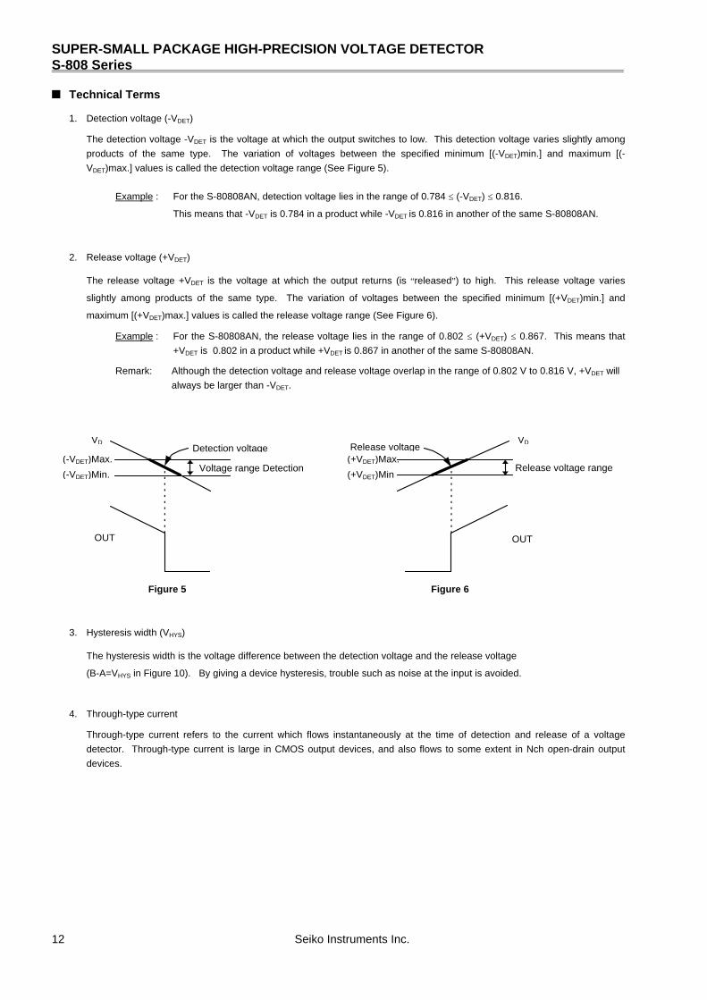
1. Detection voltage (-VDET)
The detection voltage -VDET is the voltage at which the output switches to low. This detection voltage varies slightly among
products of the same type. The variation of voltages between the specified minimum [(-VDET)min.] and maximum [(-
VDET)max.] values is called the detection voltage range (See Figure 5).
Example : For the S-80808AN, detection voltage lies in the range of 0.784 ≤ (-VDET) ≤ 0.816.
This means that -VDET is 0.784 in a product while -VDET is 0.816 in another of the same S-80808AN.
2. Release voltage (+VDET)
The release voltage +VDET is the voltage at which the output returns (is “released”) to high. This release voltage varies
slightly among products of the same type. The variation of voltages between the specified minimum [(+VDET)min.] and
maximum [(+VDET)max.] values is called the release voltage range (See Figure 6).
Example : For the S-80808AN, the release voltage lies in the range of 0.802 ≤ (+VDET) ≤ 0.867. This means that
+VDET is 0.802 in a product while +VDET is 0.867 in another of the same S-80808AN.
Remark: Although the detection voltage and release voltage overlap in the range of 0.802 V to 0.816 V, +VDET will
always be larger than -VDET.
3. Hysteresis width (VHYS)
The hysteresis width is the voltage difference between the detection voltage and the release voltage
(B-A=VHYS in Figure 10). By giving a device hysteresis, trouble such as noise at the input is avoided.
4. Through-type current
Through-type current refers to the current which flows instantaneously at the time of detection and release of a voltage
detector. Through-type current is large in CMOS output devices, and also flows to some extent in Nch open-drain output
devices.
VD
OUT
(-VDET)Max.
(-VDET)Min.Voltage range Detection
Detection voltage
Figure 5
(+VDET)Max.
(+VDET)MinRelease voltage range
VDRelease voltage
OUT
Figure 6
SUPER-SMALL PACKAGE HIGH-PRECISION VOLTAGE DETECTOR S-808 Series
Seiko Instruments Inc. 13
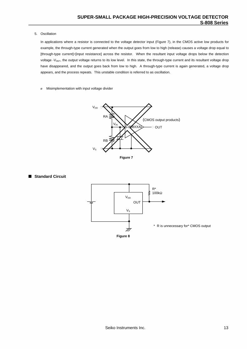
5. Oscillation
In applications where a resistor is connected to the voltage detector input (Figure 7), in the CMOS active low products for
example, the through-type current generated when the output goes from low to high (release) causes a voltage drop equal to
[through-type current]×[input resistance] across the resistor. When the resultant input voltage drops below the detection
voltage -VDET, the output voltage returns to its low level. In this state, the through-type current and its resultant voltage drop
have disappeared, and the output goes back from low to high. A through-type current is again generated, a voltage drop
appears, and the process repeats. This unstable condition is referred to as oscillation.
ù Misimplementation with input voltage divider
n Standard Circuit
RB
RA
OUTVIN
VS
VDD
S-808XXAL
(CMOS output products)
Figure 7
VDD
OUT
VS
R*100kΩ
* R is unnecessary for* CMOS output
Figure 8
SUPER-SMALL PACKAGE HIGH-PRECISION VOLTAGE DETECTORS-808 Series
14 Seiko Instruments Inc.
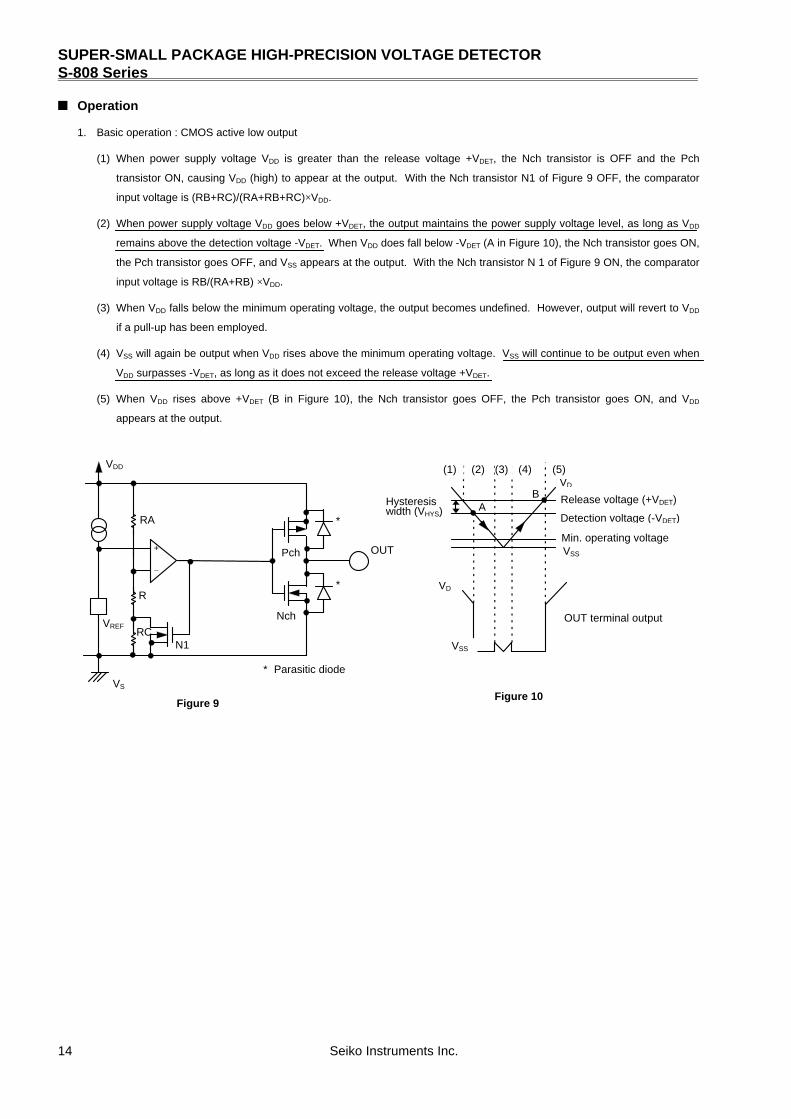
n Operation
1. Basic operation : CMOS active low output
(1) When power supply voltage VDD is greater than the release voltage +VDET, the Nch transistor is OFF and the Pch
transistor ON, causing VDD (high) to appear at the output. With the Nch transistor N1 of Figure 9 OFF, the comparator
input voltage is (RB+RC)/(RA+RB+RC)×VDD.
(2) When power supply voltage VDD goes below +VDET, the output maintains the power supply voltage level, as long as VDD
remains above the detection voltage -VDET. When VDD does fall below -VDET (A in Figure 10), the Nch transistor goes ON,
the Pch transistor goes OFF, and VSS appears at the output. With the Nch transistor N 1 of Figure 9 ON, the comparator
input voltage is RB/(RA+RB) ×VDD.
(3) When VDD falls below the minimum operating voltage, the output becomes undefined. However, output will revert to VDD
if a pull-up has been employed.
(4) VSS will again be output when VDD rises above the minimum operating voltage. VSS will continue to be output even when
VDD surpasses -VDET, as long as it does not exceed the release voltage +VDET.
(5) When VDD rises above +VDET (B in Figure 10), the Nch transistor goes OFF, the Pch transistor goes ON, and VDD
appears at the output.
AB
VD
VSS
Release voltage (+VDET)
Detection voltage (-VDET)
Min. operating voltage
OUT terminal output
Hysteresiswidth (VHYS)
VD
VSS
(1) (2) (3) (5)(4)
+
VREF
RA
−
R
RCN1
VS
VDD
Figure 9
*
OUT
*
Pch
Nch
Figure 10
* Parasitic diode

SUPER-SMALL PACKAGE HIGH-PRECISION VOLTAGE DETECTOR S-808 Series
Seiko Instruments Inc. 15
2. Other characteristics
(1) Temperature characteristic of detection voltage
The temperature characteristics of the detection voltage are expressed by the oblique line parts in Figure 11.
(2) Temperature characteristics of release voltage
(3) Temperature characteristics of hysteresis voltage
Remark: An example of temperature characteristics of (1) to (3) is shown on pages 16 and 17.
The temperature factor of the release voltage is calculated by the temperature factor of the
detection voltage as follows:
The temperature characteristics of hysteresis voltage is calculated as
∆+VDET
∆Ta-
∆-VDET
∆Ta=
VHY
-VDET×
∆-VDET
∆Ta
∆+VDET
∆Ta-
∆-VDET
∆Ta
-40 25
+0.54mV/°C
-VDET
[V]
-VDET25 is the detection voltage at 25°C-
85 Ta[°C]
-0.54mV/°C
Figure 11
S-80815AXNP:
The temperature factor of the release voltage has a same sign characteristics as the temperature factor
of the detection voltage.
∆Ta
∆-VDET×
+VDET
-VDET
=∆+VDET
∆Ta
∆Ta
∆+VDET
SUPER-SMALL PACKAGE HIGH-PRECISION VOLTAGE DETECTORS-808 Series
16 Seiko Instruments Inc.
n Characteristics (typical characteristics)
(1) Detection voltage (VDET) - Temperature (Ta)
10 40
Ta (°C)
3020-10
VDET
(V)
(a) S-80808AL (b) S-80814AL
1.3
1.35
1.4
1.45
1.5
1.55
1.6
VDET
(V)
Ta (°C)
0.76
0.74
0.78
0.8
0.82
0.84
0.86
0.88
0.9
-20 706050
+VDET
-VDET -VDET
+VDET
20 80
Ta (°C)
60400-20
VDET
(V)
(c) S-80815AL(d) S-80860AL
5.95
6.00
6.05
6.15
VDET
(V)
1.45
1.50
1.55
1.60
-40
20 8060400-20-40
6.10
6.20
6.25
-VDET
+VDET
0
+VDET
-VDET
10 403020-10-20 7060500
Ta (°C)
SUPER-SMALL PACKAGE HIGH-PRECISION VOLTAGE DETECTOR S-808 Series
Seiko Instruments Inc. 17
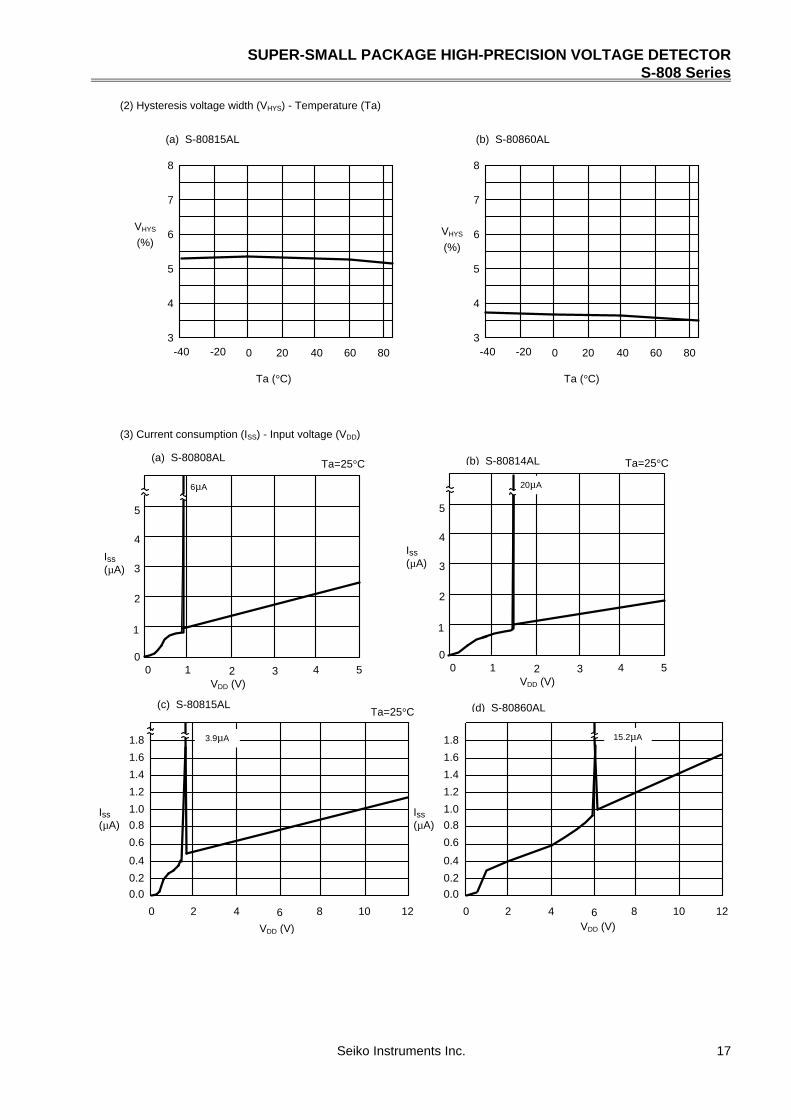
(2) Hysteresis voltage width (VHYS) - Temperature (Ta)
(3) Current consumption (ISS) - Input voltage (VDD)
Iss(µA)
(a) S-80808AL
VDD (V)
(b) S-80814AL
0 1 2 3 4 50
1
2
3
4
5
Iss(µA)
Ta (°C)
VDD (V)
(a) S-80815AL (b) S-80860AL
20 8060400
0
-20
1 2 3 4 50
1
-40
2
3
4
8
5
7
6
5
4
3
VHYS
(%)
Ta (°C)
6µA
20
20µA
8060400-20-40
8
7
6
5
4
3
VHYS
(%)
Ta=25°C Ta=25°C
Ta=25°C
Iss(µA)
(c) S-80815AL
VDD (V)
(d) S-80860AL
0 2 4 6 8 12
1.8
VDD (V)
3.9µA
10
1.6
1.4
1.2
1.0
0.8
0.6
0.4
0.2
0.0
Iss(µA)
0 2 4 6 8 12
1.8 15.2µA
10
1.6
1.4
1.2
1.0
0.8
0.6
0.4
0.2
0.0
SUPER-SMALL PACKAGE HIGH-PRECISION VOLTAGE DETECTORS-808 Series
18 Seiko Instruments Inc.
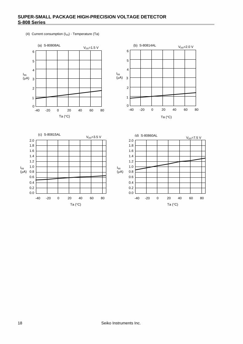
(4) Current consumption (ISS) - Temperature (Ta)
806040200-20-40 806040200-20-40
VDD=1.5 V(a) S-80808AL
Iss(µA)
0
1
2
3
4
5
6VDD=2.0 V(b) S-80814AL
Iss(µA)
0
1
2
3
4
5
6
Ta (°C)Ta (°C)
VDD=3.5 V
Iss(µA)
(c) S-80815AL (d) S-80860AL
1.8
1.6
1.4
1.2
1.0
0.8
0.6
0.4
0.2
0.0
Iss(µA)
2.0
Ta (°C) Ta (°C)
806040200-20-40
1.8
1.6
1.4
1.2
1.0
0.8
0.6
0.4
0.2
0.0
2.0
806040200-20-40
VDD=7.5 V
SUPER-SMALL PACKAGE HIGH-PRECISION VOLTAGE DETECTOR S-808 Series
Seiko Instruments Inc. 19
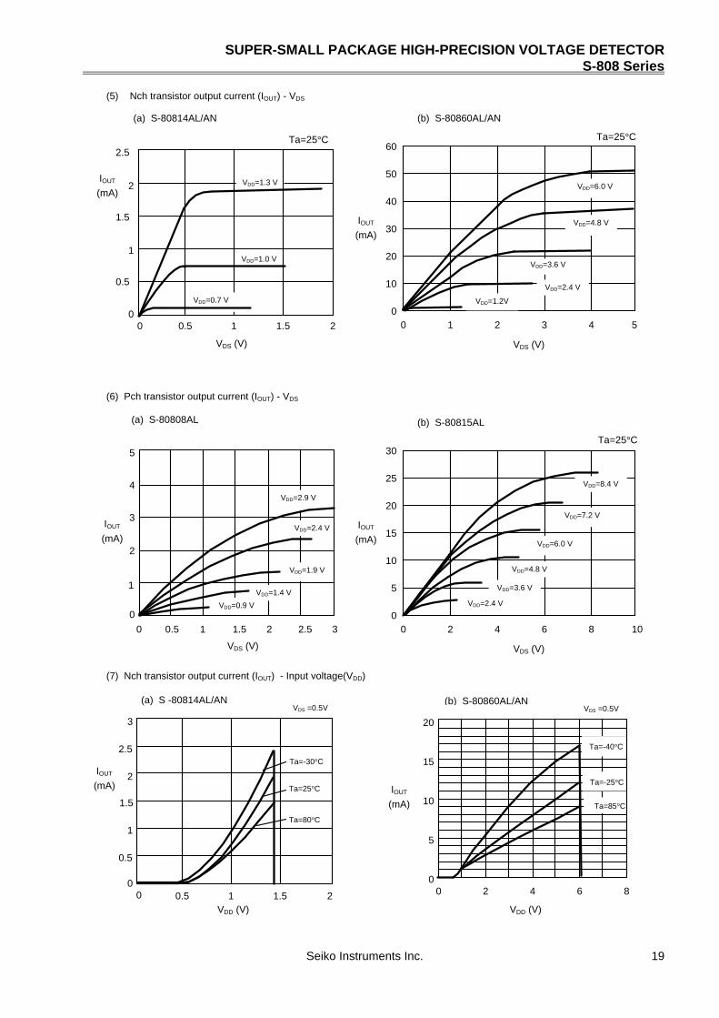
(5) Nch transistor output current (IOUT) - VDS
(6) Pch transistor output current (IOUT) - VDS
(7) Nch transistor output current (IOUT) - Input voltage(VDD)
Ta=25°CTa=25°C
Ta=25°C
VDS (V)
(a) S-80814AL/AN (b) S-80860AL/AN
IOUT
(mA)
VDS (V)
0 0.5 1 20
0.5
1
1.5
2.5
1.5
2 VDD=1.3 V
VDD=1.0 V
VDD=0.7 V
60
50
40
30
20
10
00 1 2 3 4 5
VDD=6.0 V
VDD=4.8 V
VDD=3.6 V
VDD=2.4 V
VDD=1.2V
IOUT
(mA)
(a) S-80808AL
IOUT
(mA)
VDS (V)
0
32.521.50.50 1
1
2
3
4
5
VDD=0.9 V
VDD=1.4 V
VDD=1.9 V
VDD=2.4 V
VDD=2.9 V
(b) S-80815AL
VDS (V)
30
25
20
15
10
5
00 2 4 6 8 10
IOUT
(mA)
VDD=8.4 V
VDD=7.2 V
VDD=6.0 V
VDD=4.8 V
VDD=3.6 V
VDD=2.4 V
VDS =0.5VVDS =0.5V(a) S -80814AL/AN
VDD (V)
(b) S-80860AL/AN
00
0.5
1
2
3
0.5 1 21.5
2.5
1.5
IOUT
(mA)
Ta=-30°C
Ta=25°C
Ta=80°C
20
15
10
5
00 2 4 6 8
IOUT
(mA)
Ta=-40°C
Ta=-25°C
Ta=85°C
VDD (V)
SUPER-SMALL PACKAGE HIGH-PRECISION VOLTAGE DETECTORS-808 Series
20 Seiko Instruments Inc.
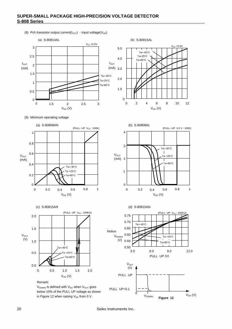
(8) Pch transistor output current(IOUT) - Input voltage(VDD)
(9) Minimum operating voltage
VDS =0.5V
Ta=80°C
Ta=25°C
Ta=-30°C
(a) S-80814AL
VDD (V)
0 1.5 2 2.5 30
0.5
1
2
3
2.5
1.5
IOUT
(mA)
VDS =0.5V
5.0
4.0
3.0
2.0
1.0
00 2 4 6 8 10 12
Ta=-40°CTa=25°C
Ta=85°C
(b) S-80815AL
VOUT
(V)1.0
(c) S-80815AN
(PULL- UP VDD : 100KΩ)
(d) S-80815AN
(PULL- UP VDD : 100KΩ)
PULL_UP (V)
0.0
0.
VDD (V)
0.5
1.5
0.5 1.0 1.5 2.0
2.0
Ta=-40°C
Ta =25°C
Ta=80°C
VDDMIN
(V)
0.75
0.70
0.65
0.60
0.55
0.503.0 6.0 9.0 12.0
Notice
VOUT
(V)
PULL_UP
PULL_UP×0.10 VDD (V)VDDMIN
Ta=-40°C
Ta =25°C
0.4
Ta=85°C
Ta =25°CVOUT
(mA)
0.6
(a) S-80808AN(PULL- UP 3.0 V : 100K)
(b) S-80808AL
VOUT
(mA)
0
1
2
3
4
0.60.40.20
(PULL- UP VDD : 100K)
0.8 1
VDD (V)
0
0.2
0.60.20 0.8 1
VDD (V)
0.4
0.8
1
Ta =25°C
Ta=80°C
Ta=80°C
Ta=-30°C
Ta=-30°C
VDD (V)
IOUT
(mA)
Figure 12
Remark:
VDDMIN is defined with VDD when VOUT goes
below 10% of the PULL UP voltage as shown
in Figure 12 when raising VDD from 0 V.
SUPER-SMALL PACKAGE HIGH-PRECISION VOLTAGE DETECTOR S-808 Series
Seiko Instruments Inc. 21
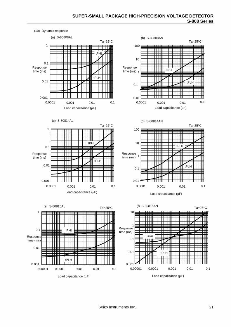
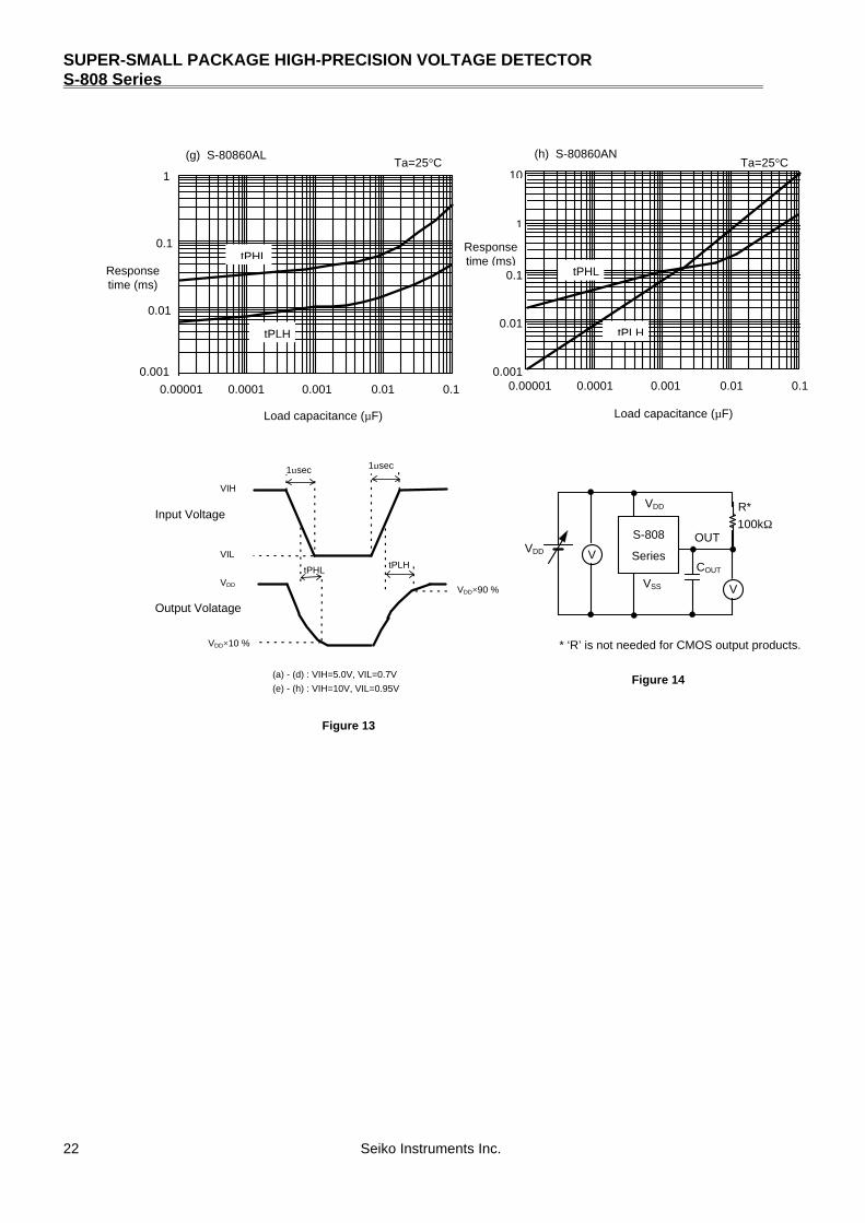
(10) Dynamic response
(e) S-80815AL
Responsetime (ms)
(a) S-80808AL (b) S-80808AN
1
(f) S-80815AN
0.1
(d) S-80814AN
0.01
0.1
1
10
100
0.0001 0.001 0.01 0.1
(c) S-80814AL
0.0001 0.001 0.01 0.1
0.001
1
0.01
0.1
tPLH
tPHL
tPLH
tPHL
Load capacitance (µF) Load capacitance (µF)
Load capacitance (µF)
Load capacitance (µF)
Responsetime (ms)
Responsetime (ms)
Responsetime (ms)
Responsetime (ms)
Response
Load capacitance (µF)
Load capacitance (µF)
Responsetime (ms)
0.01
0.1
1
10
100
0.0001 0.001 0.01 0.1
0.001
0.01
0.1
0.0001 0.001 0.01
tPLH
tPHL
tPLH
tPHL
0.001
1
0.01
0.1
0.00001 0.0001 0.001 0.01 0.1
Ta=25°C
Ta=25°C
Ta=25°C
Ta=25°C
Ta=25°C Ta=25°C
0.1
1
10
0.01
0.0010.00001 0.0001 0.001 0.01 0.1
tPHL
tPLH
tPHL
tPLH
SUPER-SMALL PACKAGE HIGH-PRECISION VOLTAGE DETECTORS-808 Series
22 Seiko Instruments Inc.
(g) S-80860AL
Load capacitance (µF)
(h) S-80860AN
Load capacitance (µF)
0.001
1
0.01
0.1
0.00001 0.0001 0.001 0.01 0.1 0.1
0.1
1
10
0.01
0.0010.00001 0.0001 0.001 0.01
tPHL
tPLH
tPHL
tPLH
Responsetime (ms)
Responsetime (ms)
COUT
VDD
VSS
OUT
VDD
V
S-808
Series
V
R*
* ‘R’ is not needed for CMOS output products.
100kΩ
VDD×90 %
VDD×10 %
VIH
VIL
VDD
tPHL tPLH
(a) - (d) : VIH=5.0V, VIL=0.7V
(e) - (h) : VIH=10V, VIL=0.95V
1µsec1µsec
Input Voltage
Output Volatage
Figure 13
Figure 14
Ta=25°C Ta=25°C
SUPER-SMALL PACKAGE HIGH-PRECISION VOLTAGE DETECTOR S-808 Series
Seiko Instruments Inc. 23
n Application Circuit Examples
1. Microcomputer reset circuits
If the power supply voltage to a microcomputer falls below the specified level, an unspecified operation may be performed or
the contents of the memory register may be lost. When power supply voltage returns to normal, the microcomputer needs to
be initialized before normal operations can be done.
Reset circuits protect microcomputers in the event of current being momentarily switched off or lowered.
With the S-808 Series which has a low operating voltage, a high-precision detection voltage and hysteresis characteristic, the
reset circuits shown in Figures 15 to 16 can be easily constructed.
2. Addition of power-on reset circuit
A power-on reset circuit can be constructed using Nch open-drain product of S-808 Series.
(Nch open-drain products)
OUTVIN
VS
VDD
Note 1: R should be 75 kΩ or less for purpose of protection against oscillation.Note 2: Di instantaneously discharges the electric charge stored by C at the falling of the power.
Di is not necessary if delay in falling time is normal.
S-808XXAN
R
C
Di
(R≤75kΩ)
VDD
(V)
t(s)
OUT(V)
t(s)Figure 17
Note 3: When the power steeply rises, output may goes high for a instant due to the IC inconstant regioncharacteristics (output voltage is unstable in the region under minimum operating voltage) as shown inFigure. 18.
VDD
(V)
t(s)
OUT(V)
t(s)
Figure 18
VS
VS
VDD
Micro-computer
S-808XXAL
Figure 15(Nch open-drain output products only)
VDD1 VDD2
Micro-computer
S-808XXAN
Figure 16
SUPER-SMALL PACKAGE HIGH-PRECISION VOLTAGE DETECTORS-808 Series
24 Seiko Instruments Inc.
3. Change of detection voltage
In Nch open-drain output products of the S-808 Series, detection voltage can be changed using resistance dividers
or diodes as shown in Figures 19 and 20. In Figure 19, hysteresis width is also changed.
n Remarks
In CMOS output products of the S-808 Series, through-type current flows when the device is detecting or releasing. If a high
impedance is connected to the input, oscillation may be caused due to the fall of the voltage by the through-type current when
lowering the voltage during releasing.
When designing for mass production using an application circuit described herein, take the product deviation and temperature
characteristic into consideration.
Seiko Instruments Inc. shall not bear any responsibility for the patents on the circuits described herein.
(Nch open-drain products)
RA
OUTVIN
VS
VDD
Note1: If RA and RB are large, the hysteresis width may belarger than the value given by the formula above dueto through-type current (which flows slightly in Nchopen-drain circuit).
Note2: RA should be 75kΩor less for purpose of protectionagainst oscillation.
+
-
S-808XXSN
Figure 19
R (Nch open-drain products)
Vf1
OUTVIN
VS
VDD
S-808XXSN
Vf2
Detection voltage = ù -VDETRA+RB
RB
Hysteresis width = ù VHYSRA+RB
RB Figure 20
Detection voltage =Vf1+Vf2+ (-VDET)
(RA≤75kΩ)
12.7±1.0
12.7±0.3(20 pitches 254.0±1.0
6.35±0.4φ4.0±0.2
0.5max.
6.0±0.5
24.7max
Marked side
1#pin 3#pin
1.0max. 1.0max.
0.7±0.2
1.45max.
Feed direction
2.5min.
Feed direction
Marked sideFtype T type
No. YF003 A C SD 1 0
φ358 2
43 0.5
53 0.5
5 0.5
45 0.5
Side Spacer(Place it in front)
33047
262
Leave enough space toaccommodate 4 components.
Spacer
32040
60
Side Spacer
165
320
Feed derection
5.2max.4.2max.
0.6max.
0.45 0.1 0.45 0.1
1.27
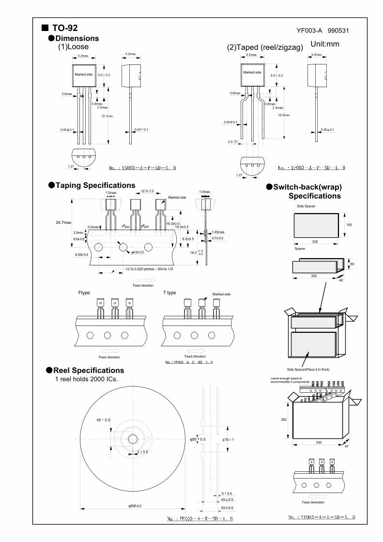
TO-92Dimensions
Taping Specifications
Reel Specifications
4.2max.
0.45 0.1
1.27
5.2max.
0.45 0.1
0.6max.
2.5 +0.4- 0.1
Switch-back(wrap)Specifications
(1)Loose (2)Taped (reel/zigzag)
YF003-A 990531
φ30 0.5
Unit:mm
1 reel holds 2000 ICs.
Marked sideMarked side
Feed direction

0.05
1 2
4 3
0∼0.1
0.15
0.16+0.1-0.06
0.30.4
1.3±0.2
1.1±0.1
0.2±0.05
2.6±0.2
T2 type
8.0±0.2
1.75±0.14.0±0.1
2.0±0.054.0±0.11.5
1.05±0.1
Feed direction
+0.1-0.05
21±0.5
2±0.2
(60°)(60°)
φ13±0.2
Winding core
Unit:mmDimensions
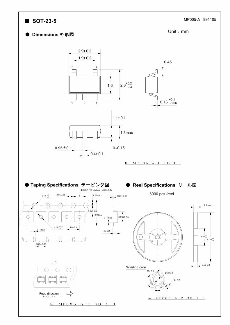
Taping Specifications Reel Specifications1 reel holds 3000 ICs.
12.5max.
9.0±0.3
SC-82ABNP004-A 990531
1.25 2.1±0.3
0.9±0.11.1max
3.5±0.1
(2.0)
φ60 +1 -0
φ180 +0 -3
3.25±0.15
ø1.5 +0.1 -0
ø1.0 +0.1 -0 4.0±0.1
2.0±0.050.27±0.05
1.4±0.2
Feed direction
SOT-23-5 MP005-A 991105
0.95 0.1
2.9±0.2
+0.1 -0.060.16
1.9±0.2
0.4±0.1
1 2 3
45
21±0.5
2±0.2
(60°)(60°)
φ13±0.2
12.5max.
9.0±0.3
+0.2 -0.32.81.6
1.1±0.1
0.45
1.3max
3 max.
3 max.
4.0±0.1 (10 pitches 40.0±0.2)
Taping Specifications Reel Specifications
Dimensions Unit mm
3000 pcs./reel
2.0±0.1
0.3±0.05
4.0±0.1 10 pitches 40.0±0.2
8.0±0.1
ø1.5+0.1 -0
2.0±0.05
ø1.5+0.1 -0
4.75±0.1
13.0±0.3
16.5max
(60°)(60°)
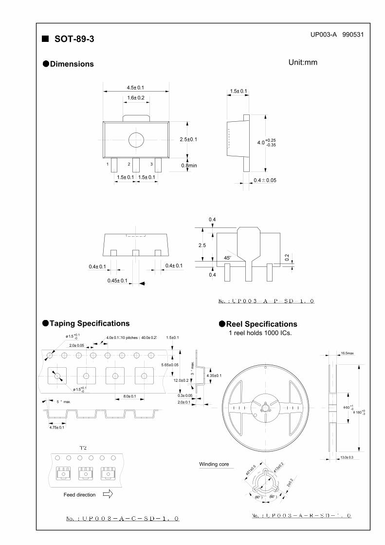
SOT-89-3UP003-A 990531
1.5±0.14.5±0.1
1.6±0.2
1.5±0.1 1.5±0.1
0.45±0.1
0.4±0.10.4±0.1
45
31 2
5 ° max.
Winding core
Unit:mmDimensions
Taping Specifications Reel Specifications1 reel holds 1000 ICs.
Feed direction
1
Markings990603
TO-92 SC-82AB
SOT-23-5 SOT-89-3
1
808
1

• The information herein is subject to change without notice.
• Seiko Instruments Inc. is not responsible for any problems caused by circuits or other diagrams
described herein whose industrial properties, patents or other rights belong to third parties. The
application circuit examples explain typical applications of the products, and do not guarantee any
mass-production design.
• When the products described herein include Strategic Products (or Service) subject to regulations,
they should not be exported without authorization from the appropriate governmental authorities.
• The products described herein cannot be used as part of any device or equipment which influences
the human body, such as physical exercise equipment, medical equipment, security system, gas
equipment, vehicle or airplane, without prior written permission of Seiko Instruments Inc.