Embed Size (px)
Citation preview
Rob
ust
Low
Power
VLSI
Robust
LowPower
VLSI
Finding the Optimal Switch Box Topology for an FPGA Interconnect
Seyi AyorindePooja Paul Chaudhury

Rob
ust
Low
Power
VLSI 2
FPGA Field
Programmable Gate Array
Reconfigurable Circuit
Configurable Logic Blocks (CLBs) Calhoun et al.: Flexible Circuits and Architectures for Ultralow Power
Rob
ust
Low
Power
VLSI 3
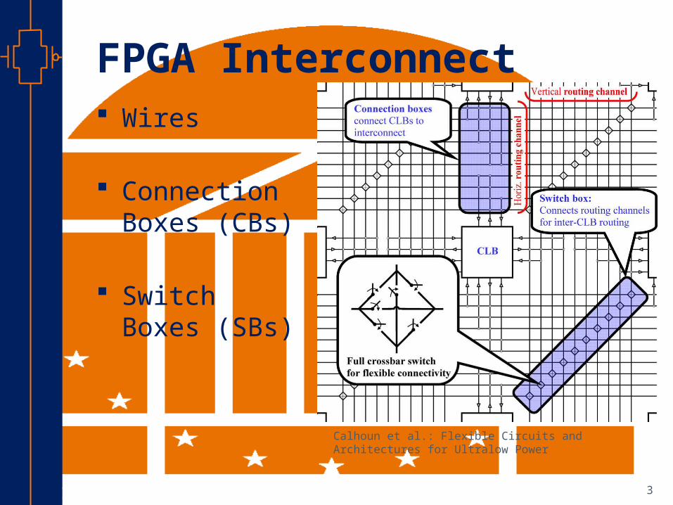
FPGA Interconnect Wires
Connection Boxes (CBs)
Switch Boxes (SBs)
Calhoun et al.: Flexible Circuits and Architectures for Ultralow Power
Rob
ust
Low
Power
VLSI 4
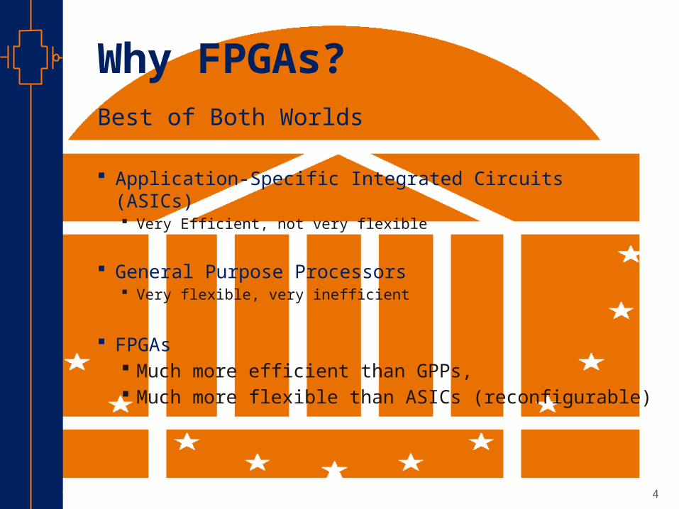
Why FPGAs?Best of Both Worlds
Application-Specific Integrated Circuits (ASICs) Very Efficient, not very flexible
General Purpose Processors Very flexible, very inefficient
FPGAs Much more efficient than GPPs, Much more flexible than ASICs (reconfigurable)
Rob
ust
Low
Power
VLSI 5
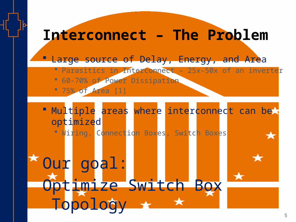
Interconnect – The Problem Large source of Delay, Energy, and Area
Parasitics in Interconnect – 25x-50x of an inverter 60-70% of Power Dissipation 75% of Area [1]
Multiple areas where interconnect can be optimized Wiring, Connection Boxes, Switch Boxes
Our goal:Optimize Switch Box Topology
Rob
ust
Low
Power
VLSI 6
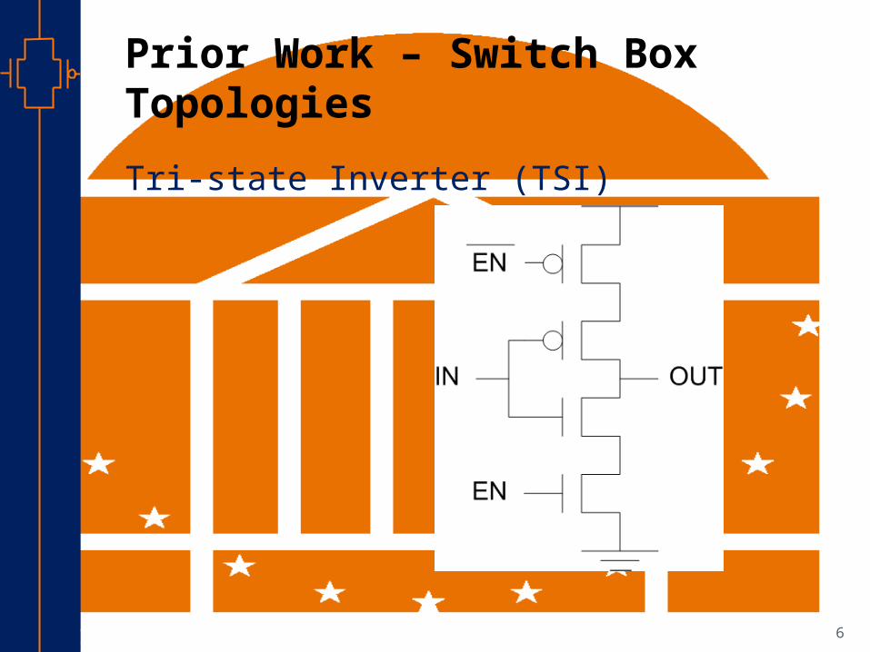
Prior Work – Switch Box Topologies
Tri-state Inverter (TSI)
Rob
ust
Low
Power
VLSI 7
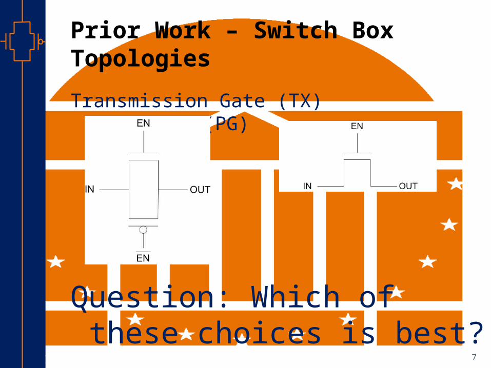
Prior Work – Switch Box Topologies
Transmission Gate (TX) Pass Gate (PG)
Question: Which of these choices is best?
Rob
ust
Low
Power
VLSI 8
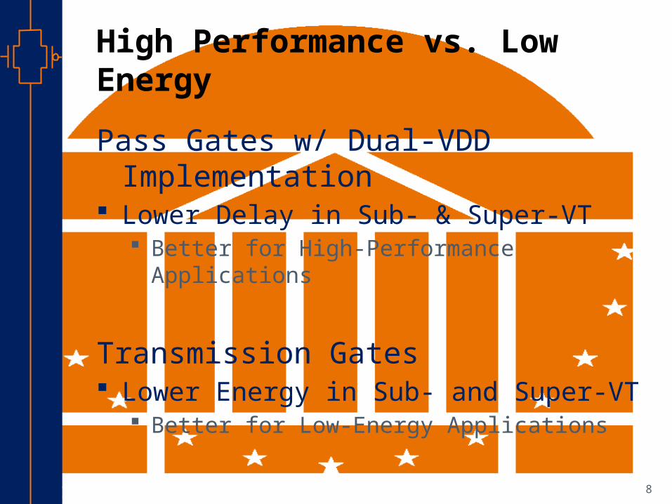
High Performance vs. Low EnergyPass Gates w/ Dual-VDD Implementation Lower Delay in Sub- & Super-VT
Better for High-Performance Applications
Transmission Gates Lower Energy in Sub- and Super-VT
Better for Low-Energy Applications
Rob
ust
Low
Power
VLSI 9
Outline Design Methodology
Test Circuits Qualifications/Assumptions
Comparison of switches w/ Single VDD scheme Comparison w/ Dual VDD scheme Conclusions
Rob
ust
Low
Power
VLSI 10
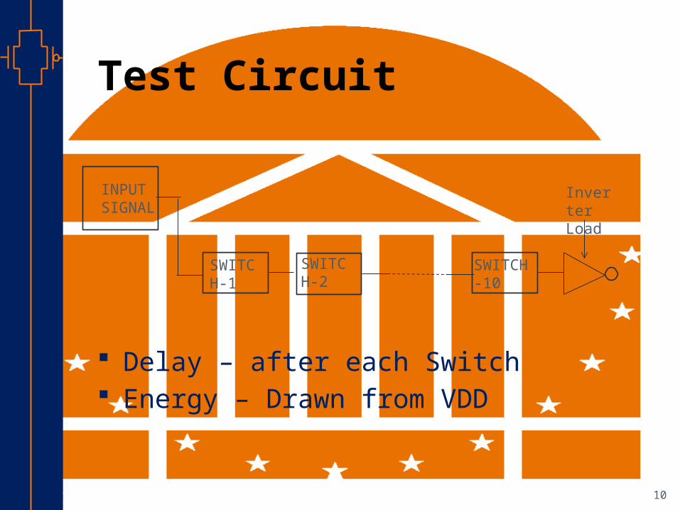
Test Circuit
Delay – after each Switch Energy – Drawn from VDD
SWITCH-1
SWITCH-2
SWITCH-10
Inverter Load
INPUT SIGNAL
Rob
ust
Low
Power
VLSI 11
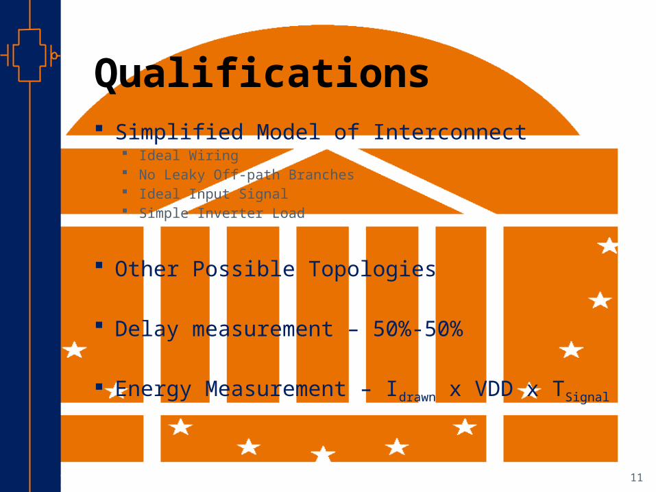
Qualifications Simplified Model of Interconnect
Ideal Wiring No Leaky Off-path Branches Ideal Input Signal Simple Inverter Load
Other Possible Topologies
Delay measurement – 50%-50%
Energy Measurement – Idrawn x VDD x TSignal
Rob
ust
Low
Power
VLSI 12
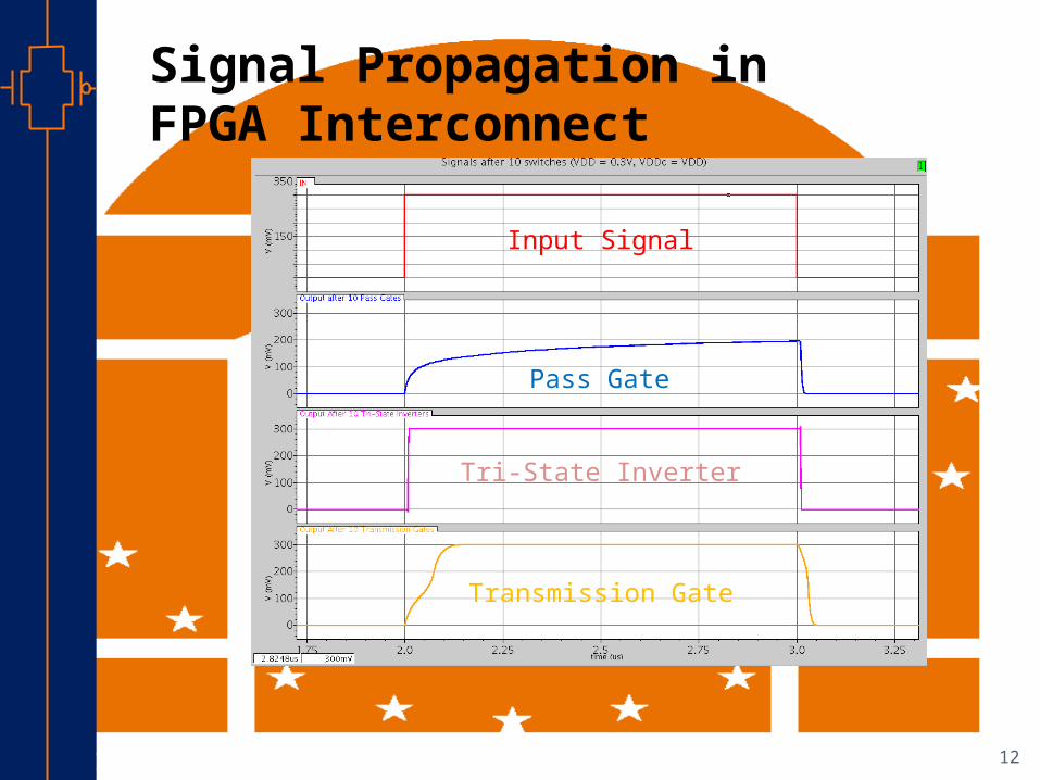
Signal Propagation in FPGA Interconnect
Pass Gate
Tri-State Inverter
Transmission Gate
Input Signal
Rob
ust
Low
Power
VLSI 13
Signal Propagation in FPGA Interconnect
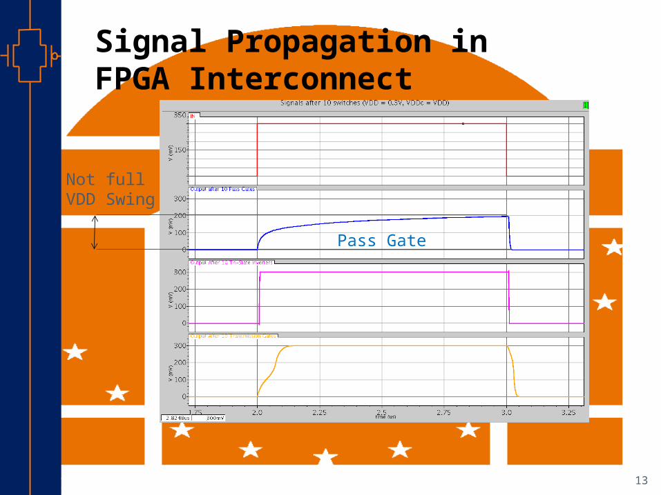
Not full VDD Swing
Pass Gate

Rob
ust
Low
Power
VLSI 14
Signal Propagation in FPGA Interconnect
Long Propagation Delay
Pass Gate
Rob
ust
Low
Power
VLSI 15
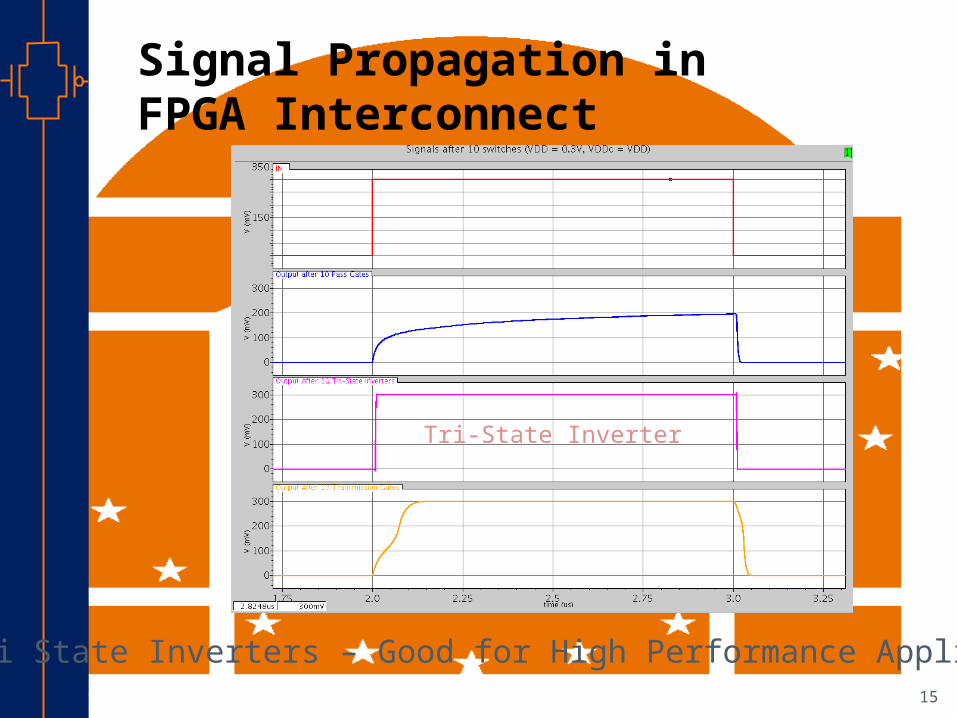
Signal Propagation in FPGA Interconnect
Tri-State Inverter
Tri State Inverters – Good for High Performance Applications

Rob
ust
Low
Power
VLSI 16
Current Draw in FPGA Interconnect
Switching Current
Rob
ust
Low
Power
VLSI 17
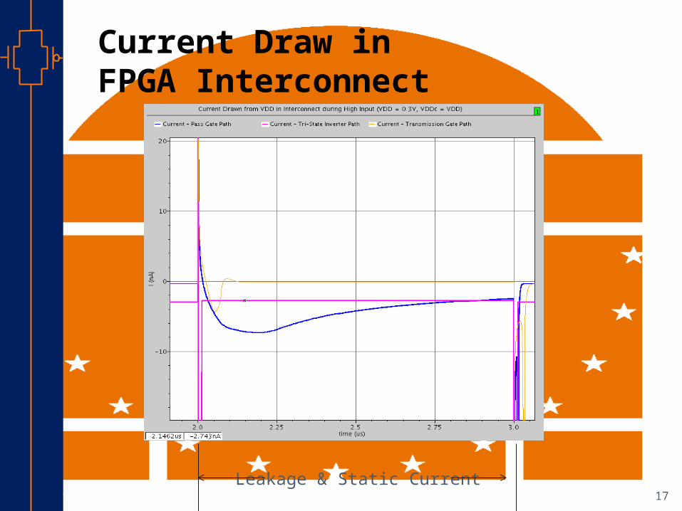
Current Draw in FPGA Interconnect
Leakage & Static Current
Rob
ust
Low
Power
VLSI 18
Current Draw in FPGA Interconnect
Pass Gate
Transmission Gate
Tri-State

Rob
ust
Low
Power
VLSI 19
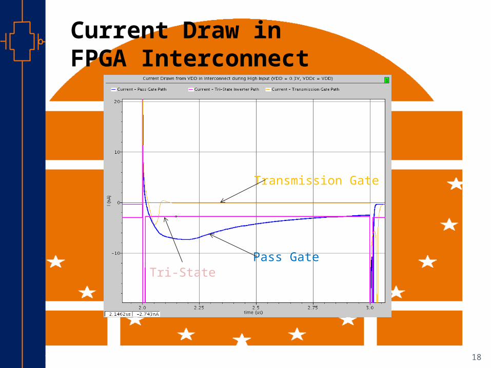
Current Draw in FPGA Interconnect
Transmission Gate
Transmission Gates – Good for Low Power Applications
Rob
ust
Low
Power
VLSI 20
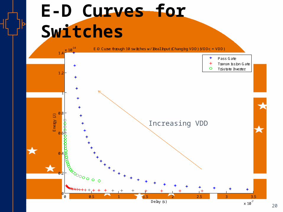
E-D Curves for Switches
0 0.5 1 1.5 2 2.5 3 3.5
x 10-7
0
0.2
0.4
0.6
0.8
1
1.2
1.4x 10
-14
Delay (s)
Ene
rgy
(J)
E-D Curve through 10 switches w/ Ideal Input (Changing VDD) (VDDc = VDD)
Pass Gate
Transmission GateTri-state Inverter
Increasing VDD
Rob
ust
Low
Power
VLSI 21
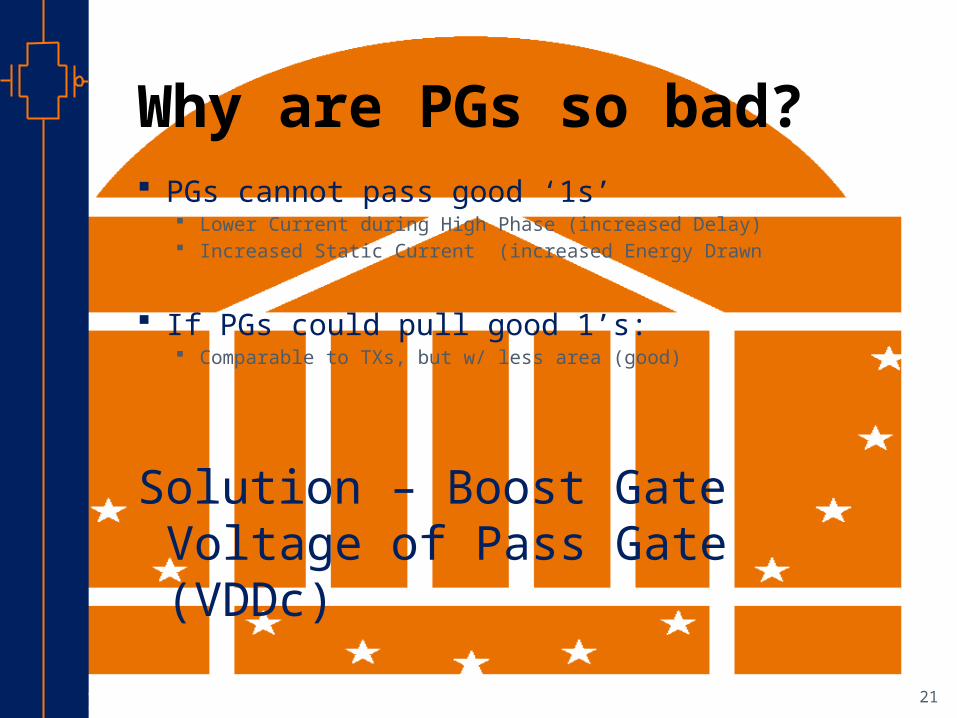
Why are PGs so bad? PGs cannot pass good ‘1s’
Lower Current during High Phase (increased Delay) Increased Static Current (increased Energy Drawn
If PGs could pull good 1’s: Comparable to TXs, but w/ less area (good)
Solution – Boost Gate Voltage of Pass Gate (VDDc)
Rob
ust
Low
Power
VLSI 22
0 0.2 0.4 0.6 0.8 1 1.2 1.4
x 10-7
2
4
6
8
10
12
14
16x 10
-16
Delay (s)
Ene
rgy
(J)
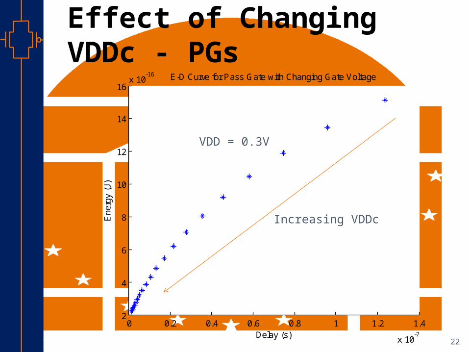
E-D Curve for Pass Gate with Changing Gate Voltage
Effect of Changing VDDc - PGs
Increasing VDDc
VDD = 0.3V
Rob
ust
Low
Power
VLSI 23
E-D Curves Revisited
0 0.5 1 1.5
x 10-7
0
1
2
3
4
5
6
7x 10
-15
Delay (s)
Ene
rgy
(J)
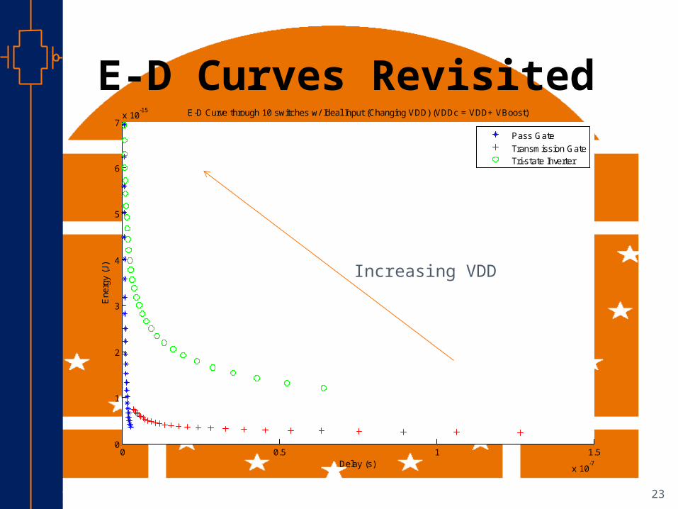
E-D Curve through 10 switches w/ Ideal Input (Changing VDD) (VDDc = VDD+ VBoost)
Pass Gate
Transmission GateTri-state Inverter
Increasing VDD
Rob
ust
Low
Power
VLSI 24
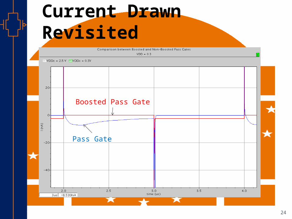
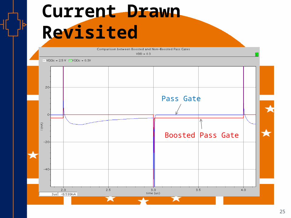
Current Drawn Revisited
Boosted Pass Gate
Pass Gate
Rob
ust
Low
Power
VLSI 25
Current Drawn Revisited
Boosted Pass Gate
Pass Gate
Rob
ust
Low
Power
VLSI 26
ConclusionsPass Gates w/ Dual VDD Scheme – Good for
High Performance
Transmission Gates – Good for Low Energy
Rob
ust
Low
Power
VLSI 27
Further Study Different Optimization of VDDc
Minimize Static Current
Dual-VDD Schemes for other topologies
Other Switch Topologies
More intricate interconnect model Wire resistance and capacitance, non-ideal signals, etc.
Rob
ust
Low
Power
VLSI 28
References[1] Calhoun, B. H., J. Ryan, S. Khanna, M. Putic, and J. Lach, "
Flexible Circuits and Architectures for Ultra Low Power", Proceedings of the IEEE, vol. 98, pp. 267-282, 02/2010.
[2] Ryan, J. F., and B. H. Calhoun, "A Sub-Threshold FPGA with Low-Swing Dual-VDD Interconnect in 90nm CMOS", Custom Integrated Circuits Conference (CICC), 20/09/2010.

Rob
ust
Low
Power
VLSI 29
Thank you!


