Embed Size (px)
Citation preview
RL-TR-91-393 AD-A 2 5 1 473Final Technical Report /December 1991
RELIABILITY OF SCHOTTKYAND OHMIC METALLIZATIONIN GaAs
Rensselaer Polytechnic Institute
A.N. Saxena and K Ramkumar
JUN 17 9-
APPROVED FORPUBLICRELASE, DISTRIBUTION UNIUMITED.
92-15798
Rome LaboratoryAir Force Systems Command
Griffiss Air Force Base, NY 13441-5700

This report has been reviewed by the Rome Laboratory Public Affairs Office(PA) and is releasable to the National Technical Information Service (NTIS). At NTISit will be releasable to the general public, including foreign nations.
RL-TR-91-393 has been reviewed and is approved for publication.
APPROVED:
LOIS H. WALSHProject Engineer
FOR THE COMMANDER:
JOHN 3. BARTTechnical Director of Reliability & Compatibility
If your address has changed or if you wish to be removed from the Rome Laboratorymailing list, or if the addressee is no longer employed by your organization, pleasenotify RL(ERDR), Griffiss AFB NY 13441-5700. This will assist us in maintaining acurrent mailing list.
Do not return copies of this report unless contractual obligations or notices on aspecific document require that it be returned.

Form ApprovedREPORT DOCUMENTATION PAGE J_0MB No. 0704-0188Pucept * b r I1a hretwcab~ictian dkmifonmt m is m~a dtwmd m I hoLar per mpa-w rmcUWkMtI- "ta1r ~ mwwn i .uri -mrdra . u
es
ga'wrg" w rrw'ltw g rcm rcid a-d vW wn -m ocd d . Sw'd wmrrwt: m ig tVoii "b~rrm aa ewwoo" w asp= dl f'.s
cclcmnd kliuv m tLck v.Ueinsb ft reaO r ts hzLzdor to Watigtn mdqiws Swvb O@W* fc ItRaTIg OpinUWs a3RWits, 1 ?i 5 JefteSom
Ovai Highwq, SL* 1204, AdnP, VA 22-43OZ Wv dt0V Ol d MWuqWTW wd&. Pawauoc Rudj Ptco (071&-0 Wswgw DC 25
1. AGENCY USE ONLY (Leave Blank) 2. REPORT DATE a REPORT TYPE AND DATES COVERED
December 1991 Final May 90 - May 91
4. TITLE AND SUBTITLE 5, FUNDING NUMBERS
RELIABILITY OF SCHOTTKY AND OHMIC METALLIZATION IN GaAs C - F30602-88-D-0028PE - 61102F
6. AUTHOR(S) PR - 2306
A. N. Saxena and K. Ramkumar TA - J4mwU - P3
7. PERFORMING ORGANIZATION NAME(S) AND ADDRESS(ES) 8. PERFORMING ORGANIZATION
Rensselaer Polytechnic Institute REPORT NUMBER
Troy NY 12180 N/A
9. SPONSORING/MONITORING AGENCY NAME(S) AND ADDRES$(ES) 10. SPONSORING/MONITORINGAGENCY REPORT NUMBER
Rome Laboratory (ERDR)
Griffiss AFB NY 13441-5700 RL-TR-91-393
I1i. SUPPLEMENTARY NOTES
Rome Laboratory Project Engineer: Lois H. Walsh/ERDR/(315) 330-4055
Prime Contractor: University of Dayton, 300 College Park, Dayton OH 45469
S12a. DISTRIBUTION/AVALABILY STATEMENT 12b. DISTRIBUTION CODE
Approved for public release; distribution unlimited.
13. ABSTRACT(m iw-rn 2wo.)
A study was undertaken on the reproducibility and reliability of AuGeNi ohmic contacts
(with a barrier layer of Ag) to n-GaAs using a limited number of as available samples.
The study showed that there is a large spread in the value of specific contact
resistance among the samples and even within each chip or wafer which means that the
reproducibility is poor. The contact resistance degrades (increasing by a factor of
up to 5) beyond a temperature of 300'C-350*C even for relatively short durations of
aging. There is also a significant variation in the aging behavior of different
contacts on the chip. Under an electrical stress, the large area contacts are stable
at 200'C while the small area contacts show significant degradation in specific
contact resistance after about 10 hours of aging. The studies carried out of the
reliability of Ti/Pt/Au Schottky contacts on n-GaAs showed that the saturation
currents increase by 4 to 5 orders of magnitude beyond a temperature of 300°C-350°C.
14. SUBJECT TERMS 15 NUMBER OF PAGES
GaAs, Ohmic Contact, Schottky Contact, Contact Resistance, 32
Reliability, AuGeNi Contact, V-I Characteristics 16 PRICECODE
17. SECURITY CLASSIFICATION 18. SECURITY CLASSIFICATION 19. SECURITY CLASSIFICATION 20. UMITATION OF ABSTRACTOF REPORT OF THIS PAGE OF A S
UNCLASSIFIED UNCLASSIFIED U
NSN 7540201 0 U1 A).l5E 51 3 O v F t S ?96 Z". c @Psawc by ANSI S%; Z20 -

EVALUATION
This contract was intended to provide valuableinformation on the reliability of contacts to GaAs. Theobjective of this research program was to understand andmodel ohmic and Schottky contacts and their degradation uponaging. The reproducibility and the dependence of contactresistance on contact size, contact metallurgy, semiconductorsheet resistance and surface concentration in available teststructures were evaluated. However, the modeling for theohmic contact in order to predict the contact resistance as afunction of various structural parameter, the process ofcontact formation and the behavior of the contact with agingwas not attempted.
I 1 -, . .. j
LOIS H. WALSHMaterials Research EngineerReliability Physics Branch
Accession For
NTIS T.A&IDTIC TA-6C
. . "
f''' ..hll7Ce

Summary
The work described in this report was carried out to evaluate the reproducibility and thereliability of contact resistance in AuGeNi ohmic contacts to n-GaAs in as available sam-ples. In the study on the reproducibility in the limited number of samples, it was found thatthere is a large spread in the values of specific contact resistance (pc) among the samples andeven within each chip/wafer. In the studies on reliability, the aging behavior of the contactsat high temperatures was examined. These studies revealed that the AuGeNi contacts witha barrier layer of Ag, are stable up to about 3000C. with the pc varying within only 5 - 10percent over long periods like 5 - 10 hrs. Beyond these temperatures, the contacts showconsiderable degradation with the p, increasing by a factor of 4 to 5 when aging is doneat 4500C for short durations like 20 to 40 mins. During the high temperature aging, thelarge area contacts (area:4500 sq.microns) showed a unique recovery behavior of p, beforeundergoing failure. The small area contacts (area:25 sq.microns) however do not show anyrecovery behavior. It was also found that there is a large variation in the aging behavior ofdifferent contacts on the same chip. ;4!oough their initial pc values are almost same. Whenthe contacts were aged at 200°C with an electrical stress applied, it was found that the largearea contacts are stable for long periods like 50 hrs and more, while the small area contactsshow significant degradation with the pc increasing by almost 100% in about 10 hrs. However.if the initial value of p, is low in the small area contacts, they do not degrade as rapidly asthose having higher values of p,. This is consistent with the model of joule heating to belargely responsible for contact degradation.
The unique aging behavior of the contacts at high temperatures indicates that complexinteractions occur at the interface involving different phases which make high resistance andlow resistance contacts to GaAs. The aging behavior with the electrical stress shows that thelocalized self heating of the contacts due to the current flow is responsible for the observeddegradation in p,.
This work has thus shed new light on the reproducibility and reliability of ohmic contactsused in GaAs MESFETs which play a crucial role in ICs used in variety of defense electronicequipment. It has brought out the following issues which need further investigation:
1. The reproducibility of p, from sample to sample needs to be improved. The variation inthe aging behavior of the contacts on the same chip should be be studied in detail.
2. There is a significant degradation of pc beyond 3500C without electrical stressing andeven at 2000C with electrical stress. In view of this, new contact metallurgies/barriermetals should be explored to achieve higher reliability.
3. The present technologies use ion implantation to realize the required sheet resistaaceof the GaAs below the contact. There is a limit to the carrier concentration ar,-,evedby this technique. This calls for new techniques to achieve higher surface conce'.rration.Further, the effective carrier concentration at the ohmic contact / GaAs interf,'ce is muchless than that predicted by the implant profile. This is due to the " deactivation - ofdopants on account of the carrier trapping by the interface states. This phenomenon wasfirst published by Saxena [8] while evaluating ohmic / Schottky contacts on degenerateSi. Similar effects are expected in the case of GaAs and other compou-d semiconductors.
41. During the aging, the sheet resistance of GaAs below the conta, t interface undergoeschanges which cannot be sensed by the presently available test structures. The six ter-minal test structure proposed bv Linholm. Mazer and Saxena 7) enables an independentmeasurement of the sheet resistance. This test structure should be incorporated into theMMIC test chip.

Some studies were also carried out on the reliability of Schottky contacts at high tempera-tures. These indicated that the contacts show significant degradation in V-I characteristicsbeyond a temperature of 3000C - 3500C. with the saturation current increasing by 4 to 5orders of magnitude and the ideality factor increasing up to about 3. This indicates thatadditional interface states are created during the aging.
ii.
Foreword
Although the ohmic contacts to GaAs. specially the AuGeNi contacts, have been studiedextensively in the past two decades [1-41. their reliability over a wide range of operatingconditions have not been established clearly vet. The metallurgical interactions that takeplace at the contact interface during the contact formation are fairly well understood throughTEM and X-ray analyses: however, the effect of aging on these interactions and i's impacton the contact resistance is not clearly understood. In this project. a study was undertakenon the aging behavior of AuGeNi contacts at high temperatures at which the effects ofthe interactions at the interface are enhanced and hence provide a better insight into thedegradation mechanisms. From the observed behavior, processes which might lead to thedegradation in p, were identified.
The reliability of Schottky contacts to GaAs has also been widely investigated. In spite ofthis, a contact metallurgy which is stable at high temperatures is still not available. TiPtA.\is one of the most widely used metallurgy. In this project some studies were made on thereliability of this contact at high temperatures. The effect of aging on the important d.cparameters of the contact was evaluated.
iii

1. Int roduction
The reliability of AuGeNi ohmic contacts to n-GaAs over a wide range of operating condi-tions is not clearly established in spite of the extensive studies carried out so far. Very littleis reported on the high temperature aging behavior of these contacts. In view of this a sys-tematic study was undertaken on the variation of contact resistance during high temperatureaging in available samples. The stability of the contacts at elevated temperatures with anapplied electrical stress was also examined. In addition. some studies were also made on theaging behavior of Schottky contacts and MESFETs. The details of the experiments carriedout and the results obtained are given below.
2. Tasks involved in the project
The following tasks were proposed to be carried out in the project1. Evaluation of Specific contact resistance (pc) of ohmic contacts to n-GaAs in available
samples
- reproducibility of Pc fom sample to sample.
- variation of p. with contact area and surface concentration.
2. Evaluation of effect of accelerated testing (witt_ time. temperature) on p. with and with-out electrical stressing.
3.Samples
The tasks mentioned above required a iarge number of samples (for studies on repro-ducibility) of various types: different semiconductor sheet resistances, different areas anddifferent contact/barrier metallurgies. However. a very limited number of samples ofonly two types were available for the studies. These samples were provided by RADC andGE (Syracuse). Three types of samples were used - 3" wafers. chips and packaged chips.These samples consist of NIMIC test structures which include Transmission line (TLM') andCross bridge (CBKR) structures for contact resistance measurement. The metallurgy of theohmic contacts in the chips was Au/Ge/Ag/Ni with an overlay of Ti/Pt/Au. The FLNlstructures had a chain of 6 contacts with spacings of 5, 10, 15. :30 and 40 microns betweenadjacent contacts. The area of each contact was 4500 sq.micron. The CBKR structureshad a chain of 7 contacts. The area of each contact was 25 sq.inicron. The test structuresare shown in fig. 1. The studies on the Schottkv contacts were made on the NIESFETstructures ( FATFET and Circuit FET structures ) available on the MIMIC test chip tfig.2).These contacts had the configuration of Ti/Pt/Au on n-GaAs.
4 .Specific tasks adldressed
In view of the samples made available, the following issues were addressed in the project:
i. Evaluation of reproducibility of p, of ohmic contacts to n-GaAs in the available samples.
I. . . .i tasks addres
nsedn nn n nn

TLM STRUCTURE CBKFL STRUCT
Fig. 1 Test structures usedi for contaict resistance measurement in ohmic contacts4---
Fi.2 MESFET tructureq |sea ir -,Liules on Schottkv contacts

ii. Evaluation of reliability of pC of ohmic contacts subjected to aging under different con-ditions of stressing (temperature, time. current).
5. Measurement of contact resistance
a. Background
The contact resistance is obtained by measurement of resistance in the TLM or CBKR teststructures. In the case of CBKR structures. the ratio of the measured voltage to currentdirectly gives the contact resistance (re). In the case of TLM structures. the ratio of themeasured voltage to current gives a resistance value which includes the sheet resistance of thesemiconductor channel between any two adjacent contacts. This resistance can be expressedas:
r = 2r, + R,.(l/w)
where R. is the sheet resistance of the semiconductor channel between adjacent contacts
I is the length of the semiconductor channel
and w is the width of the channel
w is also the width of the ohmic contact window.
If r, and r 2 are the measured resistances between two pairs of contacts with channel lengthsof 11 and 12 respectively, then
ri = 2r, + R,.(ll/w)
and r2 = 2r, + R,.(1./w)
This assumes that all the contacts have the same contact resistance.
From these r, can be obtained as:
r, = (r 112 - r21)/(2(1, - 11))
It may be noted that this r. is the "'Front" contact resistance.
In the case of CBKR structures, the Pc is related to r, by:
Pc = r,.A
where A is the contact area.
In the c& of TLM structures, pC and r, are related by:
r, = (R,.pe)'/ 2 coth [(R,/pj'/.d]
Using these relations. the p, can be obtained from the measured valus of r. in both TL.%Iand (.BKR structures.
3

b. Experimental Work
In the chips provided, the contact resistance was measured in the TLM and CBKR structures.In the case of 3" wafers, the measurements were done on the TLM structures. In themeasurement. constant currents of different values (2mA, 5mA and lOmA), of both polaritiesare passed through the structures and the corresponding voltage drops (across one contact inthe case of CBKR structures and between adjacent contacts in the case of TLM structures)are measured. From these. tile r.. and p, values are obtaii:ed.
6.Aging experiments
Most of the aging studies reported in tile literature are limited to temperatures of 2300Cto 3000C. Very little has been reported on the high temperature aging behavior of ohmiccontacts. In the present study, the ohmic contacts were aged at high temperatures of up to65001C and the behavior of P. was studied. This type of aging is required to understand andmodel the degradation/reliability mechanisms and understand the roles of the ohmic contactmetallurgies and the barrier metals. In addition to the high temperature aging, the contactswere also subjected to aging with applied electrical stress.
a. Aging without electrical stressing
In this case, the samples were aged in a furnace in a nitrogen atmosphere. Two types of agingwere done. In one type. samples were subjected to aging for short durations (ranging from15 mins to 45 mins) at successively increasing temperatures (ranging from 1500°C to 650°,C).After each aging step. the contact resistance was measured at room temperature and p, wascalculated. In the second type of aging, the samples were aged at specific temperatures overtime intervals of 20 to 60 mins each, up to a total duration of 5 to 10 hrs. In this case also.after each aging step. the contact resistance was measured and p, calculated.
b. Aging with electrical stressing
In this case, the packaged samples were aged at elevated temperatures in a temperaturecontrolled oven with specific d.c current flowing through the contacts. With the availablesetup it was possible to do aging at up to 2000C with electrical stress applied. The accuracyof temperature was ±10C and the stability was ±,IC. The TLM and CBNR structures wereaged under constant current stress for durations of 30 to 60 mins up to a total of 10 to .50lirs. After each aging step. the contact resistance was measured at room temperature and p,calculated.
7.Aging of Schottky contacts at high temperatures
Samples containing MIESFET structures were aged at high temperatures, without electricalstress, in the same way as the ohmic contacts. After each aging step. the V-I characteristicsof the Schottkv contact between the gate and channel were measured. Since packaged chipswith Schottky contacts bonded were not available, the aging behavior with electrical stresscould not be stuiled.
4

S.Results
i. Reproducibility of p. on as fabricated wafers/chips
In the 3" wafers, the measurement of contact resistance was used to generate wafer maps ofp, to show its variation across the wafer area. Typical wafer map is shown in fig. 3. Fromthis it can be seen that there is a variation of 10 to 20 % across the wafer.
In the case of chips. the p, was obtained from the two TLNI and one CBKR structures. Thevalues of p. obtained for the samples tested are shown in Table-I. The table shows that thereis a large spread in the values of p, from .,,nple to sample and within each sample. Withineach sample. the CBKR structures generally gave the lowest value of p. (lower by typically2 to 3 times or more as compared to the value given by the TLM structures). Between thesamples there is a variation of up to 2 orders of magnitude in the p. obtained from the TLMstructures.
ii. Reliability of p.
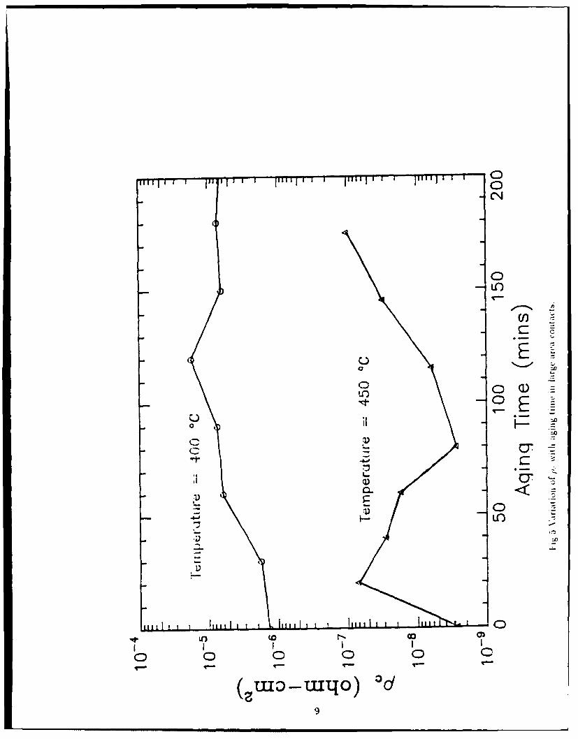
a. Aging behavior of large area ohmic contacts at high temperatures
Figs.4 and 5 show the typical variations of 1., (obtained from TLM structures) with aiin,temperature and aging time respectively. These figures show a unique recovery behavior ofthe contact resistance in both types of aging as described below. This behavior has not vetbeen reported in the literature.
In the case of aging at different temperatures, the p,, starts to increase at around 2500C to:3500('. reaches a peak at around 4000C to 4500C and subsequently decreases. On furtherincrease in aging temperature. p, increases beyond the peak value but ultimately drops off toa very low value indicating catastrophic failure of the contact. 'With increase in the durationof each aging step, the peak in the p, variation shifts to lower temperatures.
In the case of aging at a specific temperature (isochronal annealing), with increase in agin,time. the p, increases initially, reaches a peak and subsequently decreases. On further aging.the p, increases again but ultimately drops off to a very low value as in the case of aginat different temperatures. \Vith increase in aging temperature, the peak in the p variationoccurs at smaller values of aging time.
Thus. in both types of aging, a unique recovery behavior of p, is observed. A qualitativeexplanation for this behavior is given below. TEM analyses could not be performed toconfirm the validity of this explanation.
Microstructural analyses of the AuGeNi contact interface, reported in the literature i.5.61.have shown that it is comprised of Ni 2GeAs. .\u and AuGa phases which are formed duringthe alloying. In the regions which contain the Ni.2GeAs. the GaAs lavers below the contactget heavily doped by the Ge and hence these show very low contact resistance. The regionswith AuGa or Au show very large contact resistance. Thus the p, of the contact is determinedby the extent to which Ni 2 GeAs covers the contact area as compared to AuGa and Au. andthe amount of dop:na of GaAs from NiGeAs. Further. according to Braslau's model for suchinhomogeneous contacts. the p, is also dependent on the sizes of the columnar conductingregions of the contact.
Previous studies on aging of .\uGeNi contacts have shown that the excessive out diffusion
5

7.96E-5 7.20E-5 7.54E-5 8.03E-5
6.8-4E-5 6.47E-3 6.22E-5 5.26E-5 6.92E-5 6.75E-5
6.19E-5 5.MSgE 5.g3E-5 6.05E.3 5.95E-5 6.7SE-5 6.64E-5 6.57E-5
6.20E-5 6.29E-5 6.05E-3 5.85E-5 6.15E-5 6.34E-5 6.55E-5 7.09E-5
6.02E-5 6.41E-5 5.65E-3 6.55E-5 6.1BE-5 7.04E -5
6.30E-5 6.OOE-5 6.89E-5 6.18E-5
Fig. 3 Wafer map showing the variation of p c(o hm-sq cm)
o n a 3" wvafer
6

C' y x x X~:' x x x xLn rfl N N L Lfl tL N
U-; *IL4~4 N
NAIr I I I I I I I
E- u. -= c 0 C4 C)
E- I E-I x x x x x Y. x x x x
ul (n O~ -4 tLn ~L
u~ O
w~I I I I I
0 0 u
1-1 x >i x x x x )< x x X
-4

CD
-0
0
Co-0
0
V -
(UUD*)qo '0
8
C
Go 0
CD 0 CD C
(ZLUOLu~0o
9E

of Ga and the in diffusion of Au leads to an increase in resistivity of Ga.-\s near the contactinterface which leads to an increase in pc It has also been reported that when AuGeNicontacts are aged for 10 hrs or more at 4000C there is a tendencv for Ni2(;eAs grains tosegregate and for the AuGa phase to show a liquid like flow across the contact area. Hlowever.the recovery behavior of the contacts reported here is due to an aggregate of all the processesmentioned above. As the aging progresses. initially (lower temperature or time), the effectof the out diffusion of Ga into Au dominates, giving rise to an increase in p, however atthe same time, the grain growth of Ni2,GeAs and the doping of GaAs by Ge which tend toreduce p,, also get enhanced. Beyond some point during aging (i.e. a specific temperature Wrtime), the latter effect dominates andli hence there is a net decrease in p. On further aging.the AuGa tends to dominate the contact area because of its liquid like flow. surpassing thegrain growth mechanism of Ni,GeAs. thereby leading to an increase in
In the case of aging at different temperatures. if the duration of each temperature step isincreased, all the processes for the mechanisms discussed above get enhanced in each step.Thus the peak in the p, variation occurs at lower temperatures. Similarly, in the case of agingwith time. if the temperature is increased, the changes occurring in each step get enhancedand the peak in the p. variation is shifted to lower values of time.
b. Aging behavior of small area contacts
Figs.6-7 show the observed variations of P, in (CBIKR structures with aging time and ten-perature. The figure shows that the p,. is almost constant at lower temperatures. but startsto increase at around 300 - :3.500C. Unlike in the case of large area contacts. no recovery b--havior is seen in these contacts. However, the p, tends to remain fairly constant over a rangeof temperature or time thereby suggesting that the processes responsible for the recovery (I,p, in the case of large area contacts take place in the small area contacts also. but affect thep. to a lesser extent.
b. Variation in aging behavior of contacts
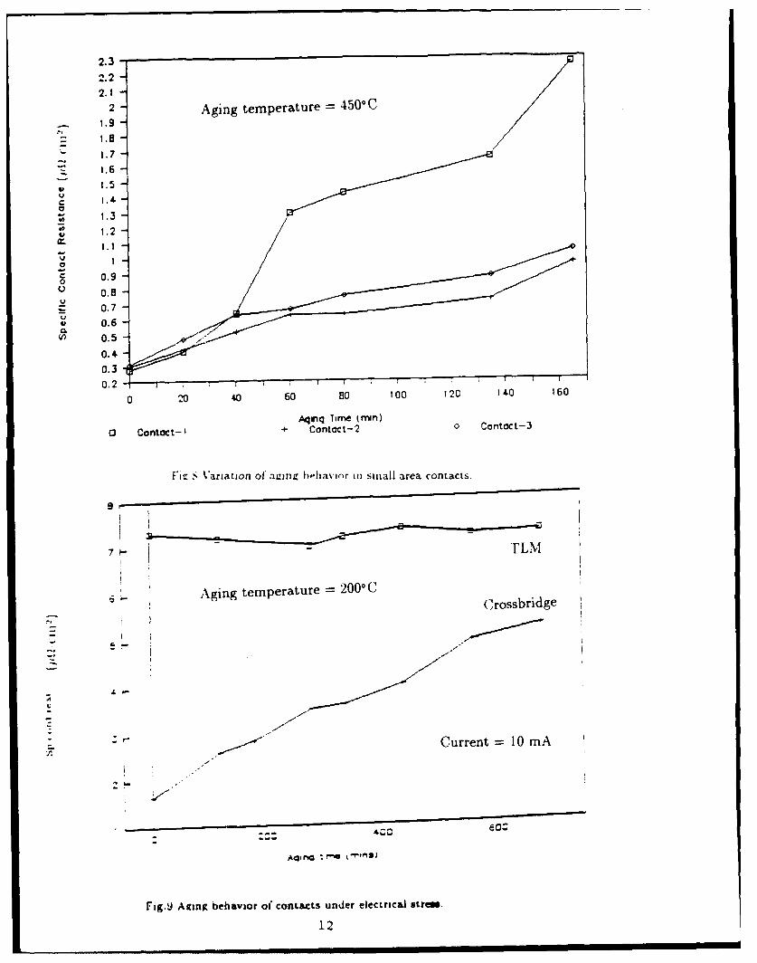
To st udv the variations in the aging behavior of contacts on the same chip. the p), of severalcontacts, in tile CBNR structure, was measured after each aging step. Fig.8 shows typicalvariations of p, of 4 contacts on a single chip during aging. From the figure, it is clear thatthere is a large difference in their aging behavior.
b. Aging behavior with applied electrical stress
Fig.9 shows the observed variation of p, with aging time for -TLM and (1BKR structuresaged at 2000C with constant current stress applied during the aging. It can he seen fromthis figure that the effect of aging on p, depends upon the current density maintained durinlthe aging. For the same current value, the effect is negligible in large area contacts in TLNIstructures (contact area: 4500 sq.microns) while it is significant in small area cross bridtestructures (contact area: 25 sq.imicrons) in which the p, increases by almost 100'/A after 1)hrs of aging. Further. even in the case of small area contacts, the degradation in p, withaging depends on the initial value. For a contact with a low initial value, the increase duringaging is very small as compared to the one with higher initial value (fig. 10). This indicatesthat a self heating mechanism (due to the power density dissipated. I?.]H/Area) is responsiblefor the observed aging behavior. This is supported by the observation that the large areacontacts in the TLM structure in which the power density is low. the degradation In /), i.negligible.
10

4.5 -
Aging time: 4.5 mins
c 2.5
C 1.5
U
E--
o200 koC
Aging lem~emture (Cl
Ig.;\ariatioll 01 %. wi arin teclIwcra1 urc in siaii arcit com'act
24-A
Aging temperature =4500 C2.2 ~
21
c
C./
C 6
2: 4: NO 2: 14: 1:
Agir: i-n 1 -rs
Fig.-, Variation of p, with altine time in smaij area contacts
2.3 -
2.2
2.1 teprtr -5C2 -Agingteprte 450
- 1.9
1.5
1.7
Z_ 1.6
W 1.5
1.31.2
CL 1.1
0 0.9o 0.5
0.6(A 0.5
0.40.3
0 20 40 60 so 100 120 140 160
Aging Time irrwn)
0 Contact- I + Contact-2 0~ Contet-3
FIz.S V~ariation of aing bhavinr ini sinall area contacts.
'77
Current 10 mA
21

0.59 -
0.55
0.57 - Aging temperature =2000C
0.56
0.55
- 0.54
* 0.53
.. 0.52
* U.~ICurrent =10 mA-. 0.5 /
C 0.49
S 0.48
V 0.47
S 0.46 /
0.45 .
0.44-
0 20 40 60 B0 100 120
Aging Tine thrs.)
Fir,.10 Azting behavior oi small area contacts withi low initial value of P, . under applied electrical stresb.
13

III Ag,,ing behavior of SchottkvN contacts
From the measured1 \-I characteristics of Schott kv conltact s after each high teruperat tireaging step. the important parametels. VIZ. thle Ideality factor n land thle saturation currentl
Ij were obtained. Typical variations of n and 1, with ag"ing Temperature anid tiiI rue ,reshown in figs. 11I and 12. These figures show liat, the contacts are st able tip to about 2(to 3000C lbevond which a significant le-gradat ion inI characteristics is seen. The sattirat loll
current Increases by I to 5 orders of magnitudl~e at temperatures around 1000C (eVen f~ iolT
dutration aging. The Idleality factor increases to about 2 to 2.7 after liiizhI t emperatutre ;itiz
This indicates that additional Interface states are create d (I uri n i, thle a ging Fu~.Ert her ',found that the degradation in ni and 1. is mnore severe III the sinal 1 area cont acts of' starndar'iiFETs as compared to the large area contact., of 1"ATFETs.
14

2.8
2.4 -Aging time =15 mins
2.3
2.2
n .1
1.9
1.7
2.6
1.4
1.3
1.2
1.1
0 200 400
Aging rem~enure (C)0 FATFET + S t. F Et
Uzi. 1() Variatic:i of idealitv factor withi azing temperature ini Schiottky contacts.
-13
-12
0
o Aging time 15i rnins
9
-7
0 200 400
Aging lern~eature (C)0 FATFET + Sid. FET
Fie. I (b) Variation oz saturation current with acine temperature in Schottky contacts

_- Aging temperature - 4000C
1.9
1 -
1 . 0 2 C3 0 C 4 0 0
Std. FEI A-n ieini FATFE7
Fig. 12(a \arlation of Ideality factor with ainutz u,, Schottky contacl
-'2.5
- 12
Aging temperature = 400'C
-11.5
CC0 1 .
0 -
0 - I
-9.5
- 8.5 ,
0 too 200 300 400
Aqiflg lime imrs)0 S t. F~ E FATFE'
Fig.12(b) Variation of iaturation current. 1%,ih ariuru time in Schottkv contacts
16

Recferences
A.Pitrowska. A.Guivarch. G.Pelous **Ohmic contacts to Ill-V compound semiconduc-tors: A review of fabrication techniques Soid State Electronics. V01.26. No.3, pp.17 9-197. 19S3.2 .~ralau Ohmic cotcst -GaAs Thin Solid Films. Vol.10-I. p.391. 1983.
2.W.J.B3oudvilke. T.C.McGill "Ohmic contacts to n-GaAs "i.Vac.Sci k- Technol. Vo1.133.1)1 1 92 . 1983.
T.Sands- ('ompouiid semiconductor contact metallurgy~ M Naterials, Science and En.-mneerin!u,.
T.S.Euani. P.E.Batson. T.N.Jackson. II.Rupprecht. E.L.\Vilke '.Electron Microscopcstudies of an alioved Au/Ni/AuGe ohmic contact to GaAs ". .J.Appi.Phys. V01.54. No. 12.pp.6952-695 7 . 1983.
..\.lurakami. N,.D.Chiids. J.NI.lakcr. .A.Callegari '- Microstructure studies of AuGe.Niohmic contacts to n-ty~pe GaAs -. J.Vac. Sci k* Technol. VoL.B4. No.4. pp.903-911.19SG.
.XA.Mazer. L.W.Linhiolm. A..N.Saxena --An improved test structure and Kelvin measure-ment method for the determination of integrated circuit contact resistance~ .1. Elect rochcem.SocVol.132. pp.440-443. 19S5.
..Saxena -- Forward curreni-voltaze characteristics and differential resistance peakof a Schottky barrier diode oni heavilyv doped Silicon **Appl.Phys.Lett. Vl1.No.1.pp1.11-13, 1969.
17

MISSION
OF
ROME LABORATORY
Rome Laboratory plans and executes an interdisciplinary program in re-
search, development, test, and technology transition in support of AirForce Command, Control, Communications and Intelligence (C31) activities
for all Air Force platforms. It also executes selected acquisition programsin several areas of expertise. Technical and engineering support within
areas of competence is provided to ESD Program Offices (POs) and otherESD elements tr, perform effective acquisition of C 31 systems. In addition,
Rome Laboratory's technology supports other AFSC Product Divisions, the
Air Force user community, and other DOD and non-DOD agencies. RomeLaboratory maintains technical competence and research programs in areasincluding, but not limited to, communications, command and control, battle
management, intelligence information processing, computational sciencesand software producibility, wide area surveillance/sensors, signal proces-sing, solid state sciences, photonics, electromagnetic technology, super-
conductivity, and electronic reliability/maintainability and testability.
![Reversible Conversion between Schottky and Ohmic …...field effect transistors (FETs) are considered as good candi-dates for various kinds of sensing systems[1] because of their high](https://img.dokumen.tips/doc/110x75/61002a1f59844679cb293e63/reversible-conversion-between-schottky-and-ohmic-field-effect-transistors-fets.jpg)


![Performance Comparison of Graphene Nanoribbon … the channel to metals with Schottky contacts [8, 14], therefore obtaining a Schottky barrier FET (SBFET). In addition, ohmic contacts](https://img.dokumen.tips/doc/110x75/5b26cfe77f8b9afc678b54f4/performance-comparison-of-graphene-nanoribbon-the-channel-to-metals-with-schottky.jpg)