Embed Size (px)
Citation preview

PSIM
User’s Guide
Powersim Inc.
-9

-8
PSIM User’s GuideVersion 7.0
Release 3
May 2006
Copyright © 2001-2006 Powersim Inc.
All rights reserved. No part of this manual may be photocopied or reproduced in any form or by anymeans without the written permission of Powersim Inc.
DisclaimerPowersim Inc. (“Powersim”) makes no representation or warranty with respect to the adequacy oraccuracy of this documentation or the software which it describes. In no event will Powersim or itsdirect or indirect suppliers be liable for any damages whatsoever including, but not limited to, direct,indirect, incidental, or consequential damages of any character including, without limitation, loss ofbusiness profits, data, business information, or any and all other commercial damages or losses, or forany damages in excess of the list price for the licence to the software and documentation.
Powersim Inc.
email: [email protected]://www.powersimtech.com

Contents
1 General Information1.1 Introduction 1
1.2 Circuit Structure 2
1.3 Software/Hardware Requirement 3
1.4 Installing the Program 3
1.5 Simulating a Circuit 4
1.6 Component Parameter Specification and Format 4
2 Power Circuit Components2.1 Resistor-Inductor-Capacitor Branches 7
2.1.1 Resistors, Inductors, and Capacitors 7 2.1.2 Rheostat 82.1.3 Saturable Inductor 9 2.1.4 Nonlinear Elements 10
2.2 Switches 11 2.2.1 Diode, DIAC, and Zener Diode 12 2.2.2 Thyristor and TRIAC 132.2.3 GTO, Transistors, and Bi-Directional Switch 15 2.2.4 Linear Switches 172.2.5 Switch Gating Block 19 2.2.6 Single-Phase Switch Modules 21 2.2.7 Three-Phase Switch Modules 22
2.3 Coupled Inductors 24
2.4 Transformers 26 2.4.1 Ideal Transformer 26
-7i

-6ii
2.4.2 Single-Phase Transformers 26 2.4.3 Three-Phase Transformers 29
2.5 Magnetic Elements 30 2.5.1 Winding 302.5.2 Leakage Flux Path 31 2.5.3 Air Gap 322.5.4 Linear Core 34 2.5.5 Saturable Core 34
2.6 Other Elements 36 2.6.1 Operational Amplifier 362.6.2 dv/dt Block 372.6.3 Power Modeling Block 38
2.7 Thermal Module 39 2.7.1 Device Database Editor 392.7.2 Diode Device in the Database 482.7.3 Diode Loss Calculation 492.7.4 IGBT Device in the Database 512.7.5 IGBT Loss Calculation 532.7.6 MOSFET Device in the Database 562.7.7 MOSFET Loss Calculation 58
2.8 Motor Drive Module 61 2.8.1 Reference Direction of Mechanical Systems 612.8.2 DC Machine 642.8.3 Induction Machine 662.8.4 Induction Machine with Saturation 702.8.5 Brushless DC Machine 722.8.6 Synchronous Machine with External Excitation 772.8.7 Permanent Magnet Synchronous Machine 802.8.8 Permanent Magnet Synchronous Machine with Saturation 832.8.9 Switched Reluctance Machine 87
2.9 MagCoupler Module 90
2.10 MagCoupler-RT Module 95

2.11 Mechanical Elements and Sensors 982.11.1 Mechanical Elements and Sensors 98
2.11.1.1 Constant-Torque Load 982.11.1.2 Constant-Power Load 992.11.1.3 Constant-Speed Load 1002.11.1.4 General-Type Load 1002.11.1.5 Externally-Controlled Load 101
2.11.2 Gear Box 1012.11.3 Mechanical Coupling Block 1022.11.4 Mechanical-Electrical Interface Block 102 2.11.5 Speed/Torque Sensors 1052.11.6 Position Sensors 107
2.11.6.1 Absolute Encoder 1082.11.6.2 Incremental Encoder 1082.11.6.3 Resolver 1092.11.6.4 Hall-Effect Sensor 110
3 Control Circuit Components3.1 Transfer Function Blocks 111
3.1.1 Proportional Controller 1123.1.2 Integrator 1133.1.3 Differentiator 1153.1.4 Proportional-Integral Controller 1153.1.5 Built-in Filter Blocks 116
3.2 Computational Function Blocks 117 3.2.1 Summer 1173.2.2 Multiplier and Divider 1183.2.3 Square-Root Block 1183.2.4 Exponential/Power/Logarithmic Function Blocks 119 3.2.5 Root-Mean-Square Block 1193.2.6 Absolute and Sign Function Blocks 120 3.2.7 Trigonometric Functions 120
-5iii

-4iv
3.2.8 Fast Fourier Transform Block 121
3.3 Other Function Blocks 122 3.3.1 Comparator 1223.3.2 Limiter 1223.3.3 Gradient (dv/dt) Limiter 1233.3.4 Trapezoidal and Square Blocks 123 3.3.5 Sampling/Hold Block 1243.3.6 Round-Off Block 1253.3.7 Time Delay Block 1263.3.8 Multiplexer 1273.3.9 THD Block 128
3.4 Logic Components 129 3.4.1 Logic Gates 1293.4.2 Set-Reset Flip-Flop 130 3.4.3 J-K Flip-Flop 1313.4.4 D Flip-Flop 1313.4.5 Monostable Multivibrator 132 3.4.6 Pulse Width Counter 1323.4.7 Up/Down Counter 1333.4.8 A/D and D/A Converters 134
3.5 Digital Control Module 135 3.5.1 Zero-Order Hold 1353.5.2 z-Domain Transfer Function Block 136
3.5.2.1 Integrator 1383.5.2.2 Differentiator 1393.5.2.3 Digital Filters 140
3.5.3 Unit Delay 1433.5.4 Quantization Block 1433.5.5 Circular Buffer 1443.5.6 Convolution Block 1453.5.7 Memory Read Block 1463.5.8 Data Array 1463.5.9 Stack 148

3.5.10 Multi-Rate Sampling System 148
3.6 SimCoupler Module 150 3.6.1 Set-up in PSIM and Simulink 1503.6.2 Solver Type and Time Step Selection in Simulink 153
4 Other Components4.1 Parameter File 157
4.2 Sources 1584.2.1 Time 1584.2.2 DC Source 158 4.2.3 Sinusoidal Source 159 4.2.4 Square-Wave Source 1604.2.5 Triangular Source 1614.2.6 Step Sources 1624.2.7 Piecewise Linear Source 1634.2.8 Random Source 1654.2.9 Math Function Source 1654.2.10 Voltage/Current-Controlled Sources 1664.2.11 Nonlinear Voltage-Controlled Sources 168
4.3 Voltage/Current Sensors 169
4.4 Probes and Meters 169
4.5 Voltage/Current Scopes 172
4.6 Switch Controllers 174 4.6.1 On-Off Switch Controller 1744.6.2 Alpha Controller 1754.6.3 PWM Lookup Table Controller 176
4.7 Function Blocks 179 4.7.1 Control-Power Interface Block 1794.7.2 ABC-DQO Transformation Block 1804.7.3 Math Function Blocks 181
-3v

-2v
4.7.4 Lookup Tables 1824.7.5 C Script Block 1854.7.6 External DLL Blocks 1864.7.7 Embedded Software Block 191
5 Analysis Specification5.1 Transient Analysis 193
5.2 AC Analysis 194
5.3 Parameter Sweep 198
6 Circuit Schematic Design6.1 Creating a Circuit 202
6.2 Editing a Circuit 203
6.3 Saving a File 206
6.4 Subcircuit 207 6.4.1 Creating Subcircuit - In the Main Circuit 2086.4.2 Creating Subcircuit - Inside the Subcircuit 2086.4.3 Connecting Subcircuit - In the Main Circuit 2106.4.4 Other Features of the Subcircuit 210
6.4.4.1 Passing Variables from the Main Circuit to Subcircuit 2116.4.4.2 Customizing the Subcircuit Image 2126.4.4.3 Including Subcircuits in the PSIM Element List 213
6.5 Running the Simulation 214
6.6 Managing the PSIM Library 218
6.7 Other Options 2236.7.1 Generate and View the Netlist File 2236.7.2 Set Path 2236.7.3 Settings 2246.7.4 Printing the Circuit Schematic 224
i

7 Waveform Processing7.1 File Menu 226
7.2 Edit Menu 226
7.3 Axis Menu 227
7.4 Screen Menu 228
7.5 View Menu 230
7.6 Option Menu 231
7.7 Label Menu 231
7.8 Exporting Data 231
8 Error/Warning Messages and Other Simulation Issues8.1 Simulation Issues 233
8.1.1 Time Step Selection 2338.1.2 Propagation Delays in Logic Circuits 2338.1.3 Interface Between Power and Control Circuits 2348.1.4 FFT Analysis 234
8.2 Error/Warning Messages 235
8.3 Debugging 236
-1vii

0 v
iii
1 General Information
1.1 IntroductionPSIM is a simulation software specifically designed for power electronics and motordrives. With fast simulation and friendly user interface, PSIM provides a powerfulsimulation environment for power electronics, analog and digital control, magnetics,and motor drive system studies.
This manual covers both PSIM1 and the following add-on Modules:
Motor Drive ModuleDigital Control ModuleSimCoupler ModuleThermal ModuleMagCoupler ModuleMagCoupler-RT Module
The Motor Drive Module has built-in machine models and mechanical load models formotor drive system studies.
The Digital Control Module provides discrete elements such as zero-order hold, z-domain transfer function blocks, quantization blocks, digital filters, for digital controlsystem analysis.
The SimCoupler Module provides interface between PSIM and Matlab/Simulink2 forco-simulation.
The Thermal Module provides the capability to calculate semiconductor devices losses.
The MagCoupler Module provides interface between PSIM and the electromagneticfield analysis software JMAG3 for co-simulation.
The MagCoupler-RT Module links PSIM with JMAG-RT3 data files.
In addition, PSIM supports links to third-party software through custom DLL blocks.The overall PSIM environment is shown below.
1. PSIM and SIMVIEW are copyright by Powersim Inc., 2001-20062. Matlab and Simulink are registered trademarks of the MathWorks, Inc.3. JMAG and JMAG-RT are copyright by the Japan Research Institute, Ltd., 1997-2006
Introduction 1

2
The PSIM simulation environment consists of the circuit schematic program PSIM, thesimulator engine, and the waveform processing program SIMVIEW1. The simulationprocess is illustrated as follows.
Chapter 1 of this manual describes the circuit structure, software/hardware requirement,and parameter specification format. Chapter 2 through 4 describe the power and controlcircuit components. Chapter 5 describes the specifications of the transient analysis andac analysis. The use of the PSIM schematic program and SIMVIEW is discussed inChapter 6 and 7. Finally, error/warning messages are discussed in Chapter 8.
1.2 Circuit StructureA circuit is represented in PSIM in four blocks: power circuit, control circuit, sensors,and switch controllers. The figure below shows the relationship between these blocks.
PSIMMatlab/Simulink
JMAG / - Control systems
- Finite element analysis
- Power electronics- Analog/digital control- Motor drives
- Electric machines, and other magnetic devices
Third-partySoftware
JMAG-RT
PSIM Simulator
PSIM Schematic
SIMVIEW
Circuit Schematic Editor (input: *.sch)
PSIM Simulator (output: *.smv or *.txt)
Waveform Processor (input: *.smv or *.txt)
General Information

The power circuit consists of switching devices, RLC branches, transformers, andcoupled inductors. The control circuit is represented in block diagram. Components in sdomain and z domain, logic components (such as logic gates and flip flops), andnonlinear components (such as multipliers and dividers) are used in the control circuit.Sensors are used to measure power circuit quantities and pass them to the controlcircuit. Gating signals are then generated from the control circuit and sent back to thepower circuit through switch controllers to control switches.
1.3 Software/Hardware RequirementPSIM runs in Microsoft Windows environment 2000/XP on personal computers. Theminimum RAM memory requirement is 128 MB.
1.4 Installing the ProgramA quick installation guide is provided in the flier “PSIM - Quick Guide” and on the CD-ROM.
Some of the files in the PSIM directory are shown in the table below.
Files Description
PSIM.exe PSIM circuit schematic editor
SIMVIEW.exe Waveform display program SIMVIEW
PcdEditor.exe Device database editor
s2z_converter.exe s-domain to z-domain converter
Power Circuit
Control Circuit
Sensors Switch Controllers
Software/Hardware Requirement 3

4
File extensions used in PSIM are:
1.5 Simulating a CircuitTo simulate the sample one-quadrant chopper circuit “chop.sch”:
- Start PSIM. From the File menu, choose Open to load the file “chop.sch”.
- From the Simulate menu, choose Run PSIM to start the simulation.Simulation results will be saved to File “chop.txt”.
- If the option Auto-run SIMVIEW is not selected in the Options menu, fromthe Simulate menu, choose Run SIMVIEW to start SIMVIEW. If the optionis selected, SIMVIEW will be launched automatically. In SIMVIEW, selectcurves for display.
1.6 Component Parameter Specification and FormatThe parameter dialog window of each component in PSIM has three tabs: Parameters,Other Info, and Color, as shown below.
The parameters in the Parameters tab are used in the simulation. The information in the
SetSimPath.exe Program to set up the SimCoupler Module
psim.lib, psimimage.lib PSIM library files
*.sch PSIM schematic file
*.txt PSIM simulation output file (text)
*.fra PSIM ac analysis output file (text)
*.dev Device database file
*.smv SIMVIEW data file
General Information

Other Info tab, on the other hand, is not used in the simulation. It is for reportingpurposes only and will appear in the parts list in View -> Element List in PSIM.Information such as device rating, manufacturer, and part number can be stored underthe Other Info tab.
The component color can be set in the Color tab.
Parameters under the Parameters tab can be a numerical value or a mathematicalexpression. A resistance, for example, can be specified in one of the following ways:
12.512.5k12.5Ohm12.5kOhm25./2.OhmR1+R2R1*0.5+(Vo+0.7)/Io
where R1, R2, Vo, and Io are symbols defined either in a parameter file (see Section4.1), or in a main circuit if this resistor is in a subcircuit (see Section 6.3.4.1).
Power-of-ten suffix letters are allowed in PSIM. The following suffix letters aresupported:
G 109
M 106
k or K 103
m 10-3
u 10-6
n 10-9
p 10-12
A mathematical expression can contain brackets and is not case sensitive. The followingmathematical functions are allowed:
+ addition- subtraction* multiplication/ division^ to the power of [Example: 2^3 = 2*2*2]SQRT square-root functionSIN sine functionCOS cosine function
Component Parameter Specification and Format 5

6
ASIN sine inverse functionACOS cosine inverse functionTAN tangent functionATAN inverse tangent functionATAN2 inverse tangent function [-π <= atan2(y,x) <= π]SINH hyperbolic sine functionCOSH hyperbolic cosine functionEXP exponential (base e) [Example: EXP(x) = ex]LOG logarithmic function (base e) [Example: LOG(x) = ln (x)]LOG10 logarithmic function (base 10) ABS absolute functionSIGN sign function [Example: SIGN(1.2) = 1; SIGN(-1.2)=-1]
General Information

2 Power Circuit Components
2.1 Resistor-Inductor-Capacitor Branches
2.1.1 Resistors, Inductors, and CapacitorsBoth individual resistor, inductor, capacitor, and lumped RLC branches are provided inPSIM. Initial conditions of inductor currents and capacitor voltages can be defined.
To facilitate the setup of three-phase circuits, symmetrical three-phase RLC branches,“R3”, “RL3”, “RC3”, “RLC3”, are provided. Initial inductor currents and capacitorvoltages of the three-phase branches are all zero.
Images:
For three-phase branches, the phase with a dot is Phase A.
Attributes:
Parameters Description
Resistance Resistance, in Ohm
Inductance Inductance, in H
Capacitance Capacitance, in F
Initial Current Initial inductor current, in A
Initial Cap. Voltage Initial capacitor voltage, in V
R L C RL RC
R3 RL3 RC3 RLC3
RLC
LC
Resistor-Inductor-Capacitor Branches 7

8
The resistance, inductance, or capacitance of a branch can not be all zero. At least one ofthe parameters has to be a non-zero value.
2.1.2 RheostatA rheostat is a resistor with a tap.
Image:
Attributes:
Current Flag Flag for branch current output. If the flag is zero, there is no current output. If the flag is 1, the current will be available for display in the runtime graphs (under Simulate -> Runtime Graphs). It will also be saved to the output file for display in SIMVIEW. The current is positive when it flows into the dotted terminal of the branch.
Current Flag_A; Current Flag_B; Current Flag_C
Current flags for Phase A, B, and C of three-phase branches, respectively.
Parameters Description
Total Resistance Total resistance of the rheostat R (between Node k and m), in Ohm
Tap Position (0 to 1) The tap position Tap. The resistance between Node k and t is: R*Tap.
Current Flag Flag for the current that flows into Node k.
k m
t
Power Circuit Components

2.1.3 Saturable InductorA saturable inductor takes into account the saturation effect of the magnetic core.
Image:
Attributes:
The nonlinear B-H curve is represented by piecewise linear approximation. Since theflux density B is proportional to the flux linkage λ and the magnetizing force H isproportional to the current i, the B-H curve can be represented by the λ-i curve instead,as shown below.
The inductance is defined as: L = λ / i, the ratio of λ v.s. i at each point. The saturationcharacteristics are defined by a series of data points as: (i1, L1), (i2, L2), (i3, L3), etc.
Note that the defined saturation characteristics must be such that the flux linkage λ ismonotonically increasing. That is, L1*i1 < L2*i2 < L3*i3, etc.
Also, similar to the saturation characteristics in the real world, the slope of each linearsegment must be monotonically decreasing as the current increases.
In certain situations, circuits that contain saturable inductors may fail to converge.Connecting a very small capacitor across the saturable inductor may help theconvergence.
Parameters Description
Current v.s. Inductance Characteristics of the current versus the inductance (i1, L1), (i2, L2), etc.
Current Flag Flag for the current display
i (H)
λ (B)
i1 i2 i3
λ1
λ2λ3
Inductance L = λ / i
Resistor-Inductor-Capacitor Branches 9
10
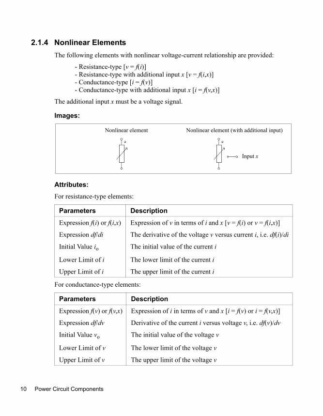
2.1.4 Nonlinear ElementsThe following elements with nonlinear voltage-current relationship are provided:
- Resistance-type [v = f(i)]- Resistance-type with additional input x [v = f(i,x)]- Conductance-type [i = f(v)]- Conductance-type with additional input x [i = f(v,x)]
The additional input x must be a voltage signal.
Images:
Attributes:For resistance-type elements:
For conductance-type elements:
Parameters Description
Expression f(i) or f(i,x) Expression of v in terms of i and x [v = f(i) or v = f(i,x)]
Expression df/di The derivative of the voltage v versus current i, i.e. df(i)/di
Initial Value io The initial value of the current i
Lower Limit of i The lower limit of the current i
Upper Limit of i The upper limit of the current i
Parameters Description
Expression f(v) or f(v,x) Expression of i in terms of v and x [i = f(v) or i = f(v,x)]
Expression df/dv Derivative of the current i versus voltage v, i.e. df(v)/dv
Initial Value vo The initial value of the voltage v
Lower Limit of v The lower limit of the voltage v
Upper Limit of v The upper limit of the voltage v
Nonlinear element Nonlinear element (with additional input)
Input x
Power Circuit Components
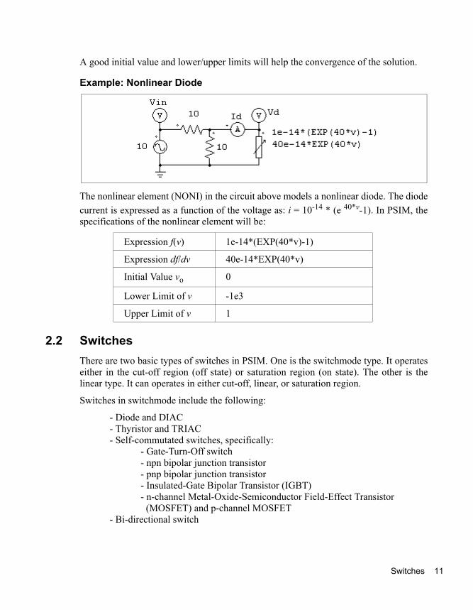
A good initial value and lower/upper limits will help the convergence of the solution.
Example: Nonlinear Diode
The nonlinear element (NONI) in the circuit above models a nonlinear diode. The diodecurrent is expressed as a function of the voltage as: i = 10-14 * (e 40*v-1). In PSIM, thespecifications of the nonlinear element will be:
2.2 SwitchesThere are two basic types of switches in PSIM. One is the switchmode type. It operateseither in the cut-off region (off state) or saturation region (on state). The other is thelinear type. It can operates in either cut-off, linear, or saturation region.
Switches in switchmode include the following:
- Diode and DIAC - Thyristor and TRIAC - Self-commutated switches, specifically:
- Gate-Turn-Off switch - npn bipolar junction transistor - pnp bipolar junction transistor - Insulated-Gate Bipolar Transistor (IGBT)- n-channel Metal-Oxide-Semiconductor Field-Effect Transistor
(MOSFET) and p-channel MOSFET - Bi-directional switch
Expression f(v) 1e-14*(EXP(40*v)-1)
Expression df/dv 40e-14*EXP(40*v)
Initial Value vo 0
Lower Limit of v -1e3
Upper Limit of v 1
Switches 11

12
Switch models are ideal. That is, both turn-on and turn-off transients are neglected. Aswitch has an on-resistance of 10μΩ and an off-resistance of 10MΩ. Snubber circuitsare not required for switches.
Linear switches include the following:
- npn bipolar junction transistor - pnp bipolar junction transistor
2.2.1 Diode, DIAC, and Zener DiodeThe conduction of a diode is determined by circuit operating conditions. A diode isturned on when it is positively biased, and is turned off when the current drops to zero.
Image:
Attributes:
A DIAC is a bi-directional diode. A DIAC does not conduct until the breakover voltageis reached. After that, the DIAC goes into avalanche conduction, and the conductionvoltage drop is the breakback voltage.
Image:
Attributes:
Parameters Description
Diode Voltage Drop Diode conduction voltage drop, in V
Initial Position Flag for the initial diode position. If the flag is 0, the diode is off. If it is 1, the diode is on.
Current Flag Current flag of the diode.
Parameters Description
Breakover Voltage Voltage at which breakover occurs and the DIAC begins to conduct, in V
Power Circuit Components

A zener diode is modelled by a circuit as shown below.
Images:
Attributes:
When the zener diode is positively biased, it behaviors as a regular diode. When it isreverse biased, it will block the conduction as long as the cathode-anode voltage VKA isless than the breakdown voltage VB. When VKA exceeds VB, the voltage VKA will beclamped to VB. [Note: when the zener is clamped, since the diode is modelled with anon-resistance of 10μΩ, the cathode-anode voltage will in fact be equal to: VKA = VB +10μΩ * IKA. Therefore, depending on the value of IKA, VKA will be slightly higher thanVB. If IKA is very large, VKA can be substantially higher than VB].
2.2.2 Thyristor and TRIACA thyristor is controlled at turn-on. The turn-off is determined by circuit conditions.
A TRIAC is a device that can conduct current in both directions. It behaviors in thesame way as two opposite thyristors connected in parallel.
Breakback Voltage Conduction voltage drop, in V
Current Flag Current flag
Parameters Description
Breakdown Voltage Breakdown voltage VB of the zener diode, in V
Forward Voltage Drop Voltage drop of the forward conduction (diode voltage drop from anode to cathode), in V
Current Flag Flag for zener current output (from anode to cathode)
ZenerCircuit Model
A
K
A
K
VB
Switches 13

14
Images:
Attributes:
Note that for the TRIAC device, the holding current and latching current are set to zero.
There are two ways to control a thyristor or TRIAC. One is to use a gating block, andthe other is to use a switch controller. The gate node of a thyristor or TRIAC must beconnected to either a gating block or a switch controller.
The following examples illustrate the control of a thyristor switch.
Examples: Control of a Thyristor Switch
Parameters Description
Voltage Drop Thyristor conduction voltage drop, in V
Holding Current Minimum conduction current below which the device stops conducting and returns to the OFF state (for thyristor only)
Latching Current Minimum ON state current required to keep the device in the ON state after the triggering pulse is removed (for thyristor only)
Initial Position Flag for the initial switch position (for thyristor only)
Current Flag Flag for switch current output
Thyristor
A KGate
TRIAC
Gate
Gating Block
Alpha Controller
Power Circuit Components

This circuit on the left uses a switching gating block. The switching gating pattern andthe frequency are pre-defined, and remain unchanged throughout the simulation. Thecircuit on the right uses an alpha switch controller. The delay angle alpha, in deg., isspecified through the dc source in the circuit.
2.2.3 GTO, Transistors, and Bi-Directional SwitchSelf-commutated switches in the switchmode, except pnp bipolar junction transistor(BJT) and p-channel MOSFET, are turned on when the gating signal is high (when avoltage of 1V or higher is applied to the gate node) and the switch is positively biased(collector-emitter or drain-source voltage is positive). It is turned off whenever thegating signal is low or the current drops to zero.
For pnp BJT and p-channel MOSFET, switches are turned on when the gating signal islow and switches are negatively biased (collector-emitter or drain-source voltage isnegative).
A GTO switch is a symmetrical device with both forward-blocking and reverse-blockingcapabilities. An IGBT or MOSFET switch consist of an active switch with an anti-parallel diode.
A bi-directional switch conducts currents in both directions. It is on when the gatingsignal is high and is off when the gating signal is low, regardless of the voltage biasconditions.
Note that a limitation of the BJT switch model in PSIM, in contrary to the devicebehavior in the real life, is that a BJT switch in PSIM will block reverse voltage (in thissense, it behaviors like a GTO). Also, it is controlled by a voltage signal at the gate node,not a current.
Images:
BJT( BJT Bi-directionalGTO IGBTMOSFETMOSFET(p-channel) (n-channel) switch(npn) (pnp)
Switches 15

16
Attributes:
A switch can be controlled by either a gating block or a switch controller. They must beconnected to the gate (base) node of the switch. The following examples illustrate thecontrol of a MOSFET switch.
Examples: Control of a MOSFET Switch
The circuit on the left uses a gating block, and the one on the right uses an on-off switchcontroller. The gating signal is determined by the comparator output.
Example: Control of a npn Bipolar Junction Transistor The circuit on the left uses a gating block, and the one on the right uses an on-off switchcontroller.
Parameters Description
Initial Position Initial switch position flag. For MOSFET and IGBT, this flag is for the active switch, not for the anti-parallel diode.
Current Flag Switch current flag. For MOSFET and IGBT, the current through the whole module (the active switch plus the diode) will be displayed.
On-off Controller
Power Circuit Components

The following shows another example of controlling the BJT switch. The circuit on theleft shows how a BJT switch is controlled in the real life. In this case, the gating voltageVB is applied to the transistor base drive circuit through a transformer, and the basecurrent determines the conduction state of the transistor.
This circuit can be modelled and implemented in PSIM as shown on the right. A diode,Dbe, with a conduction voltage drop of 0.7V, is used to model the pn junction betweenthe base and the emitter. When the base current exceeds 0 (or a certain threshold value,in which case the base current will be compared to a dc source), the comparator outputwill be 1, applying the turn-on pulse to the transistor through the on-off switchcontroller.
2.2.4 Linear SwitchesLinear switches include npn bipolar junction transistor and pnp bipolar junctiontransistor. They can operate in either cut-off, linear, or saturation region.
Images:
BJT (npn) BJT (pnp)
Switches 17
18
Attributes:
A linear BJT switch is controlled by the base current Ib. It can operate in one of the threeregions: cut-off (off state), linear, and saturation region (on state). The properties ofthese regions for the npn transistor are:
- Cut-off region: Vbe < Vr; Ib = 0; Ic = 0- Linear region: Vbe = Vr; Ic = β∗Ib; Vce > Vce,sat- Saturation region: Vbe = Vr; Ic < β∗Ib; Vce = Vce,sat
where Vbe is the base-emitter voltage, Vce is the collector-emitter voltage, and Ic is thecollector current.
Note that for both the npn and pnp transistors, the gate node (base node) is a powernode, and must be connected to a power circuit component (such as a resistor or asource). It can not be connected to a gating block or a switch controller.
WARNING: It has been found that the linear model for npn and pnptransistors works well in simple circuits, but may not work whencircuits are complex. Please use this model with caution.
Examples: Circuits Using the Linear BJT SwitchExamples below illustrate the use of linear switches. The circuit on the left is a linearvoltage regulator circuit, and the transistor operates in the linear mode. The circuit onthe right is a simple test circuit.
Parameters Description
Current Gain beta Transistor current gain β, defined as: β=Ic/Ib
Bias Voltage Vr Forward bias voltage, in V, between base and emitter for the npn transistor, or between emitter and base for the pnp transistor.
Vce,sat [or Vec,sat for pnp]
Saturation voltage, in V, between collector and emitter for the npn transistor, and between emitter and collector for the pnp transistor.
Power Circuit Components

2.2.5 Switch Gating BlockA switch gating block defines the gating pattern of a switch or a switch module. Thegating pattern can be specified either directly (the element is called Gating Block in thelibrary) or in a text file (the element is called Gating Block (1) in the library).
Note that a switch gating block can be connected to the gate node of a switch ONLY. Itcan not be connected to any other elements.
Image:
Attributes:
The number of switching points is defined as the total number of switching actions inone period. Each turn-on or turn-off action is counted as one switching point. Forexample, if a switch is turned on and off once in one cycle, the number of switchingpoints will be 2.
Parameters Description
Frequency Operating frequency of the switch or switch module connected to the gating block, in Hz
No. of Points Number of switching points (for the Gating Block element only)
Switching Points Switching points, in deg. If the frequency is zero, the switching points is in second. (for the Gating Block element only)
File for Gating Table
Name of the file that stores the gating table (for the Gating Block (1) element only)
NPN_1
NPN_1
Switches 19

20
For the Gating Block (1) element, the file for the gating table must be in the samedirectory as the schematic file. The gating table file has the following format:
nG1G2... ...Gn
where G1, G2, ..., Gn are the switching points.
Example:Assume that a switch operates at 2000 Hz and has the following gating pattern in oneperiod:
The specification of the Gating Block element for this switch will be:
The gating pattern has 6 switching points (3 pulses). The corresponding switchingangles are 35o, 92o, 175o, 187o, 345o, and 357o, respectively.
If the Gating Block (1) element is used instead, the specification will be:
The file “test.tbl” will contain the following:
635.92.175.187.
Frequency 2000.
No. of Points 6
Switching Points 35. 92. 175. 187. 345. 357.
Frequency 2000.
File for Gating Table test.tbl
0 180 360
9235 175 187 345 357
(deg.)
Power Circuit Components

345.357.
2.2.6 Single-Phase Switch ModulesBuilt-in single-phase diode bridge module and thyristor bridge module are provided.The images and internal connections of the modules are shown below.
Images:
Attributes:
Node Ct at the bottom of the thyristor module is the gating control node for Switch 1.For the thyristor module, only the gating signal for Switch 1 needs to be specified. Thegating signals for other switches will be derived internally in the program.
Similar to the single thyristor switch, a thyristor bridge can also be controlled by either agating block or an alpha controller, as shown in the following examples.
Examples: Control of a Thyristor Bridge The gating signal for the circuit on the left is specified through a gating block, and thegating signal for the circuit on the right is provided through an alpha controller. A majoradvantage of the alpha controller is that the delay angle alpha of the thyristor bridge, indeg., can be directly controlled.
Parameters Description
Diode Voltage Drop or Voltage Drop
Forward voltage drop of each diode or thyristor, in V
Init. Position_i Initial position for Switch i
Current Flag_i Current flag for Switch i
A+
A-
Diode bridge Thyristor bridgeDC+
DC-
A+
A-
DC+
DC-
1 3
4 2 24
1 3
Ct
A+
A-
DC+
DC-
A+
A-
DC+
DC-
Ct
Switches 21

22
2.2.7 Three-Phase Switch ModulesThe following figure shows three-phase switch modules and the internal circuitconnections. A three-phase voltage source inverter module VSI3 consists of eitherMOSFET-type or IGBT-type switches. A current source inverter module CSI3 consistsof GTO-type switches, or equivalently IGBT in series with diodes.
Images:
Thyristor half-wave (3-phase) Thyristor half-wave
A
B
C
A1
1
2
6
1
2
3
A6
A
B
C
NNN N
Ct
Ct
Ct
Ct
B
A
C
Diode full-wave Thyristor full-waveDC+
DC-
A
B
C
DC+
DC-
1 3 5
4 6 2
1 3 5
4 6 2
A AB BC C
DC-
DC+
DC-
DC+
Ct
Ct
Power Circuit Components

Attributes:
Similar to single-phase modules, only the gating signal for Switch 1 need to be specifiedfor three-phase modules. Gating signals for other switches will be automaticallyderived. For the 3-phase half-wave thyristor bridge, the phase shift between twoconsecutive switches is 120o. For all other bridges, the phase shift is 60o.
Thyristor bridges can be controlled by an alpha controller. Similarly, voltage/current
Parameters Description
On-Resistance On resistance of the MOSFET switch during the on state, in Ohm (for MOSFET-type switches only)
Saturation Voltage Conduction voltage drop of the IGBT switch, in V (for IGBT-type switches only)
Voltage Drop Conduction voltage drop of the switch, in V (for CSI3 only)
Diode Voltage Drop Conduction voltage drop of the anti-parallel diode, in V (for VSI3 only)
Init. Position_i Initial position for Switch i
Current Flag_i Current flag for Switch i
CSI3
VSI3
A
B
C
DC+
DC-
A
B
C
1 3 5
24 6
1 3 5
24 6
DC-
DC+
DC-
DC+
DC-
DC+
CBA
CBA
Ct
Ct
Ct
Ct
VSI3 (MOSFET switches)
CSI3
Switches 23

24
source inverters can be controlled by a PWM lookup table controller.
The following examples illustrate the control of three-phase thyristor and voltage sourceinverter modules.
Example: Control of Three-Phase Thyristor and VSI Modules
The thyristor circuit on the left uses an alpha controller. For a three-phase circuit, thezero-crossing of the voltage Vac corresponds to the moment when the delay angle alphais equal to zero. This signal is used to provide synchronization to the controller.
The circuit on the right uses a PWM lookup table controller. The PWM patterns arestored in a lookup table in a text file. The gating pattern is selected based on themodulation index. Other inputs of the PWM lookup table controller include the delayangle, the synchronization, and the enable/disable signal. A detailed description of thePWM lookup table controller is given in the Switch Controllers section.
2.3 Coupled InductorsCoupled inductors with two, three, and four branches are provided.
Images:
PWM ControllerVac
2-branch 3-branch 4-branch
Power Circuit Components

Attributes:
In the images, the circle, square, triangle, and plus marks refer to Inductor 1, 2, 3, and 4,respectively.
The following shows a coupled inductor with two branches.
Let L11 and L22 be the self-inductances of Branch 1 and 2, and L12 and L21 the mutualinductances, the branch voltages and currents have the following relationship:
The mutual inductances between two windings are assumed to be always equal, i.e., L12= L21.
Example: Two mutually coupled inductors have the self inductances and mutual inductance as:L11 = 1 mH, L22 = 1.1 mH, and L12 = L21 = 0.9 mH. The specification of this elementwill be:
Parameters Description
Lii (self) Self inductance of the inductor i, in H
Lij (mutual) Mutual inductance between Inductor i and j, in H
ii_initial Initial current in Inductor i
Iflag_i Flag for the current printout in Inductor i
L11 (self) 1m
L12 (mutual) 0.9m
L22 (self) 1.1m
i1
i2
v1
v2
+ -
+ -
v1
v2
L11 L12
L21 L22
ddt----- i1
i2
⋅=
Coupled Inductors 25

26
2.4 Transformers
2.4.1 Ideal TransformerAn ideal transformer has no losses and no leakage flux.
Images:
The winding with the larger dot is the primary, and the other winding is the secondary.
Attributes:
Since the turns ratio is equal to the ratio of the rated voltages, the number of turns can bereplaced by the rated voltage at each side.
2.4.2 Single-Phase TransformersThe following single-phase transformer modules are provided:
- Transformer with 1 primary and 1 secondary windings - Transformer with 1 primary and 2 secondary windings - Transformer with 2 primary and 2 secondary windings - Transformer with 1 primary and 4 secondary windings - Transformer with 2 primary and 4 secondary windings - Transformer with 1 primary and 6 secondary windings - Transformer with 2 primary and 6 secondary windings
Parameters Description
Np (primary) No. of turns of the primary winding
Ns (secondary) No. of turns of the secondary winding
Np Ns Np Ns
Power Circuit Components

Images:
In the images, p refers to primary, s refers to secondary, and t refers to tertiary.
The winding with the largest dot is the primary winding or first primary winding. Forthe multiple winding transformers, the sequence of the windings is from the top to thebottom.
For the transformers with 2 or 3 windings, the attributes are as follows.
Attributes:
Parameters Description
Rp (primary); Rs (secondary);Rt (tertiary)
Resistance of the primary/secondary/tertiary winding, in Ohm
Lp (pri. leakage); Ls (sec. leakage);Lt (ter. leakage)
Leakage inductance of the primary/secondary/tertiary winding, in H (seen from the primary)
Lm (magnetizing) Magnetizing inductance, in H
Np (primary); Ns (secondary);Nt (tertiary)
No. of turns of the primary/secondary/tertiary winding
5-winding
p
s_1
s_4
5-winding
p_1
p_2
s_1
s_3
4-winding
p_1
p_2
s_1
s_2
8-winding
p_1
p_2
s_1
s_2
s_6
2-winding 3-winding 7-winding
p st
p
p
ss_1
s_6
s_2
sp
2-windinge
6-winding
p_1
p_2
s_1
s_4
Transformers 27

28
All the resistances and inductances are referred to the primary winding side. If there aremultiple primary windings, they are referred to the first primary winding side.
For the transformers with more than 1 primary winding or more than 3 secondarywindings, the attributes are as follows.
Attributes:
All the resistances and inductances are referred to the first primary winding side.
Modeling of a Transformer: A transformer is modeled as coupled inductors. For example, a single-phase two-winding transformer is modeled as two coupled inductors. The equivalent circuit can beshown as:
In the circuit, Rp and Rs are the primary and secondary winding resistances; Lp and Ls arethe primary and secondary winding leakage inductances; and Lm is the magnetizinginductance. All the values are referred to the primary side.
Example: A single-phase two-winding transformer has a winding resistance of 0.002 Ohm andleakage inductance of 1 mH at both the primary and the secondary side (all the valuesare referred to the primary). The magnetizing inductance is 100 mH, and the turns ratio
Parameters Description
Rp_i (primary i); Rs_i (secondary i)
Resistance of the ith primary/secondary/tertiary winding, in Ohm
Lp_i (pri. i leakage); Ls_i (sec. i leakage)
Leakage inductance of the ith primary/secondary/tertiary winding, in H (referred to the first primary winding)
Lm (magnetizing) Magnetizing inductance, in H (seen from the first primary winding)
Np_i (primary i); Ns_i (secondary i)
No. of turns of the ith primary/secondary/tertiary winding
Lp Ls
Lm
Ideal
Rp Rs Np : Ns
SecondaryPrimary
Power Circuit Components

is Np:Ns = 220:440. The transformer will be specified as:
2.4.3 Three-Phase TransformersTwo-winding and three-winding transformer modules are provided, as shown below.They all have 3-leg cores.
- 3-phase transformer (windings unconnected) - 3-phase Y/Y and Y/Δ connected transformer - 3-phase 3-winding transformer (windings unconnected) - 3-phase 3-winding Y/Y/Δ and Y/Δ/Δ connected transformer - 3-phase 4-winding transformer (windings unconnected)
Images:
Rp (primary) 2m
Rs (secondary) 2m
Lp (primary) 1m
Ls (secondary) 1m
Lm (magnetizing) 100m
Np (primary) 220
Ns (secondary) 440
Y/Y Y/D D/D
Y/Y/D Y/D/D
2-winding (unconnected)
A
B
C
A+A-B+B-C+C-
A
B
C
a
b
c
A
B
C
a
b
c
a
b
c
N n
aa+
a+a-b+b-c+c-N
A
B
C
abc
aabbcc
A
B
C
abc
aabbcc
N
n
N
A+A-B+B-C+C-
a+a-b+b-c+c-
aa-bb+bb-cc+
cc-
3-winding (unconnected) 4-winding (unconnected)
A+A-B+B-C+C-
AA+AA-BB+BB-CC+CC-
a+a-b+b-c+c-aa+aa-bb+bb-cc+cc-
Transformers 29

30
Attributes:
In the images, P refers to primary, S refers to secondary, and T refers to tertiary. Allresistances and inductances are referred to the primary or the first primary winding side.
Three-phase transformers are modeled in the same way as single-phase transformers.
2.5 Magnetic ElementsA set of magnetic elements, including winding, leakage flux path, air gap, linear core,and saturable core, is provided to model magnetic devices. These elements are the basicbuilding blocks of magnetic equivalent circuits, and they provide a very powerful andconvenient way of modeling any types of magnetic devices.
2.5.1 WindingA winding element provides the interface between the electric circuit and the magneticequivalent circuit.
Image:
Parameters Description
Rp (primary); Rs (secondary);Rt (tertiary)
Resistance of the primary/secondary/tertiary winding, in Ohm
Lp (pri. leakage); Ls (sec. leakage);Lt (ter. leakage)
Leakage inductance of the primary/secondary/tertiary winding, in H
Lm (magnetizing) Magnetizing inductance, in H (seen from the primary side)
Np (primary); Ns (secondary);Nt (tertiary)
No. of turns of the primary/secondary/tertiary winding
E1
M2E2
M1
Power Circuit Components

Attributes:
This element represents a winding on a magnetic core. The two electric nodes (E1 andE2) are connected to an electric circuit, while the two magnetic nodes (M1 and M2) areconnected to other magnetic elements (such as leakage flux path, air gap, and magneticcore).
2.5.2 Leakage Flux PathThis element models the flow path of the leakage flux.
Image:
Attributes:
The resistance R represents the losses due to the leakage flux. Assuming that the mmf(magnetomotive force) applied across the leakage flux path is F, the electric equivalentcircuit of the leakage flux path is as follows:
Parameters Description
Number of Turns No. of turns of the winding
Winding Resistance Winding resistance, in Ohm
Parameters Description
Inductance Factor AL Inductance factor AL, defined as the inductance per turn squared
Resistance for Losses Resistance R, in Ohm, that represents the losses due to the leakage flux.
Current Flag Display flag of the current that flows through the resistor R
M1 M2
Magnetic Elements 31

32
The mmf, in the form of a voltage source, applies across the capacitor (the capacitanceis AL) and the resistor R. Let the current flowing through this branch be i, and the rmsvalue be Irms, the relationship between the losses due to the leakage flux and theresistance R is:
2.5.3 Air GapThe image and attributes of an air gap element are as follows.
Image:
The input parameters of the air gap can be defined in two ways. One is to define the airgap length and the cross section area, and the other is to define the inductance factor AL.They are as follows.
Attributes:
For the element Air Gap:
Parameters Description
Air Gap Length The length of the air gap, lg, in m
Cross Section Area Cross section of the air gap, Ac, in m2
Resistance for Losses Resistance R, in ohm, that represents the losses due to the air gap fringing effect
Current Flag Display flag of the current that flows through the resistor R
+ i
-
F
AL
R
Ploss Irms2 R⋅=
M1 M2
Power Circuit Components

For the element Air Gap (1):
The resistance R represents the losses due to the air gap fringing effect. Assuming thatthe mmf (magnetomotive force) applied across the air gap is F, the electric equivalentcircuit of the air gap is as follows:
The mmf, in the form of a voltage source, applies across the capacitor (the capacitancehas the value of the inductance factor AL) and the resistor R. For the element Air Gap,the inductance factor can be calculated from the air gap length and the cross section areaas:
where μo= 4π∗10−7.
The losses on the resistor represents the losses due to the fringing effect, which can beexpressed as:
where Irms is the rms value of the current i flowing through the resistor.
Parameters Description
Inductance Factor AL Inductance factor AL, defined as the inductance per turn squared
Resistance for Losses Resistance R, in ohm, that represents the losses due to the air gap fringing effect
Current Flag Display flag of the current that flows through the resistor R
+ i
-
F
AL
R
ALμo Ac⋅
lg----------------=
Ploss Irms2 R⋅=
Magnetic Elements 33

34
2.5.4 Linear CoreThis element represents a linear lossless core.
Image:
Attributes:
If the length of the core is Llength and the cross section area is Ac, the inductance factorAL is expressed as:
where μr is the relative permeability of the core material.
2.5.5 Saturable CoreThis element models a magnetic core with saturation and hysteresis.
Image:
Parameters Description
Inductance Factor AL Inductance factor AL of the core, defined as the inductance per turn squared
M1 M2
ALμo μr Ac⋅ ⋅
Llength-------------------------=
C1
M1 M2
Power Circuit Components

Attributes:
In the element image, the nodes M1 and M2 are the two nodes that connect to othermagnetic elements (such as winding, flux leakage path, air gap, etc.), and the node C1 isan output node that shows the flux of the core. By connecting a voltage probe to thisnode, the flux of the core can be displayed. Node C1 is a control circuit node.
The coefficients K1, Kexp1, K2, and Kexp2 are used to fit the B-H curve of an actualmagnetic material. Coefficient K1 usually varies between 0.7 and 1, depending on thecore material. Coefficient Kexp1 mainly affects the rate of the core saturation, and is inthe range between 10 and 200 (10 for low permeability ferrite, and 200 for metglas).
The coefficients K2 and Kexp2 are used in very rare occasions, such as for ferroresonantregulators. They are normally set as follows to keep them from affecting the B-H curve:
K2 > 2
Kexp2 > 20
Parameters Description
Inductance Factor AL Inductance factor AL of the core, defined as the inductance per turn squared
Resistance for Losses Resistance R, in Ohm, that represents the core losses
Saturation Flux Density Bm
Flux density Bm at saturation, in Tesla
Coefficient K1 Coefficient K1 for the core B-H curve
Coefficient Kexp1 Coefficient Kexp1 for the core B-H curve
Coefficient K2 Coefficient K2 for the core B-H curve
Coefficient Kexp2 Coefficient Kexp2 for the core B-H curve
Current Flag Display flag of the current that flows through the resistor R
Magnetic Elements 35

36
2.6 Other Elements
2.6.1 Operational AmplifierThree op. amp. elements are provided in the PSIM Library: Op. Amp., Op. Amp. (1), andOp. Amp. (2).
An ideal operational amplifier (op. amp.) is modelled using power circuit elements, asshown below.
Images:
where
Attributes:
V+; V- - noninverting and inverting input voltages
Vo - output voltage
A - op. amp. gain (A is set to 100,000.)
Ro - output resistance (Ro is set to 80 Ohms)
Parameters Description
Voltage Vs+ Upper voltage source level of the op. amp.
Voltage Vs- Lower voltage source levels of the op. amp.
V+
V-Vo
Op. Amp.
Circuit Model of the Op. Amp.
V+
V-Vo
V+
V-
Vo
Vs+Vs-
Ro
A*(V+ - V-)
gnd
Op. Amp. (1)
gnd
V+
V-
Vo
Op. Amp. (2)
gnd
Power Circuit Components

The difference between the element Op. Amp. and Op. Amp. (1) or Op. Amp. (2) is that,for the Op. Amp. element, the reference ground of the op. amp. model is connected tothe power ground, whereas for Op. Amp. (1) or Op. Amp. (2), the reference ground nodeof the model is accessible and can be floating.
Note that the image of an op. amp. is similar to that of a comparator. For the op. amp.,the inverting input is at the upper left and the noninverting input is at the lower left. Forthe comparator, it is the opposite.
Example: A Boost Power Factor Correction CircuitThe figure below shows a boost power factor correction circuit. The PI regulators ofboth the inner current loop and the outer voltage loop are implemented using op. amp.
2.6.2 dv/dt BlockA dv/dt block has the same function as the differentiator in the control circuit, exceptthat it is for the power circuit.
Image:
The output of the dv/dt block is equal to the derivative of the input voltage versus time.It is calculated as:
Comparator
VoVin t( ) Vin t Δt–( )–
Δt----------------------------------------------=
Other Elements 37

38
where Vin(t) and Vin(t-Δt) are the input values at the current and previous time step, andΔt is the simulation time step.
2.6.3 Power Modeling BlockThe Power Modeling Block is a type of external DLL block that allows users to definealgebraic and differential equations for a device, and to build a model in the powercircuit. Unlike conventional DLL blocks that have signal inputs and signal outputs withno consideration of the power conservation (no input and output power balance), thePower Modeling Block allows electric currents to flow in and out of the terminals, andmaintains the power balance.
The Power Modeling Block provides a very powerful way of modeling power devices.It can have power terminals, control input/output terminals, and mechanical shaftterminals, and equations can be either algebraic or differential, linear or nonlinear. Asignificant feature of the Power Modeling Block is that these equations are assembledand solved simultaneously with the other equations from the rest of the PSIM circuit,resulting a very robust, stable, and efficient solution.
For more information on how to use the Power Modeling Block, refer to the document"Help Power Modeling Block.pdf".
Power Circuit Components

2.7 Thermal ModuleThe Thermal Module is an add-on module to the basic PSIM program. It provides aquick way of estimating the losses of semiconductor devices (diodes, IGBT, andMOSFET).
The core of the Thermal Module is the device database. A device database editor isprovided to allow users to add new devices to the database and to manage the databaseeasily. The devices in the database can then be used in the simulation for the losscalculation.
The following illustrates the process of how a device in the database is used in thesimulation and how the losses are calculated:
- The behavior model of the device is used in the simulation. The behavior modeltakes into account the static characteristics of the device (such as conductionvoltage drop, on-state resistance, etc.), but not the dynamic characteristics (such asturn-on and turn-off transients).
- Based on the voltage and current values from the simulation, PSIM accesses thedevice database and calculates the conduction losses or switching losses. The staticcharacteristics of the device are updated for the next simulation.
Please note that the loss calculation is only approximation and the accuracy of theresults depends on the accuracy of the device data, as well as proper scaling of theresults from the device test condition to the actual circuit operating conditions. Usersshould always verify the results with the measurement from the hardware setup.
The following sections describe how a device is added to the database, and how it isused in the simulation.
2.7.1 Device Database EditorThe device database editor, PcdEditor.exe, provides an easy and convenient way ofadding, editing, and managing devices. An image of the database editor is shown below.
On the left are the device database files that are loaded into the database editor, and thelist of the devices. The devices can be displayed based on either Device Type orManufacturer. Also, the device list can be sorted by Part Number, Voltage rating, orCurrent rating, by clicking on the title bars of the list.
On the right is the information of each device. In general, the following information isdefined for the device:
- Manufacturer and Part Number- Package type- Absolute maximum ratings
Thermal Module 39

40
- Electrical characteristics- Thermal characteristics- Dimension and weight
To create a new device file, choose File -> New Device File. To load a device files intothe editor, choose File -> Open Device File. To unload a device file from the editor,choose File -> Close Device File.
Three types of devices can be added to a device files: diode, IGBT, and MOSFET.However, since dual IGBT-diode modules have a different set of parameters ascompared to the regular IGBT devices, they are treated as a separate type (referred to asthe IGBT-DIODE type). The sections that follow describe in more details each type ofdevices.
To create a new device, go to the Device menu, and choose either New Diode, NewIGBT, New IGBT-Diode, or New MOSFET.
To make a copy of an existing device in the same database file, highlight the device inthe list, and choose Device -> Save Device As. To make a copy of an existing deviceand save it in a different database file, first highlight the device in the list, then highlightthe file name in the File Name list, and choose Device -> Save Device As.
Devicedatabasefiles
Devicelist
Deviceinformation
Power Circuit Components

Adding a Device to the Database:
To illustrate how to add a device to a database file, below is the step-by-step procedureto add the Powerex discrete diode CS240650 (600V, 50A) into the device database file"diode_new.dev".
- Launch PcdEditor.exe. Go to File -> New Device File, and create a file called"diode_new.dev". This file will be placed in the device sub-folder under thePSIM program folder by default.
- With the file name "diode_new" highlighted in the "File Name" list, ChooseDevice -> New Diode. A diode will be added to the database file withManufacturer as "New" and Part Number as "New".
- Obtain the datasheet of Powerex diode CS240650 from the web sitewww.pwrx.com. Show the PDF file of the datasheet on the screen.
- By referring to the information from the datasheet, in the database editor, enterthe following information for this device:
Manufacturer: PowerexPart Number: CS240650Package: Discrete
and under Absolute Maximum Ratings:
Vrrm,max (V): 600IF,max (A): 50Tj,max (oC): 150
- Define the forward voltage characteristics Vd v.s. IF under ElectricalCharacteristics by clicking on the Edit button on top of the Vd v.s. IF graph area.
The following dialog window will appear. The dialog window has two pages:Graph and Conditions.
The Graph page contains thee x and y axis settings as well as the data points andthe graph. In this case, the y axis is the conduction voltage drop Vd, and the x axisis the forward current IF. The x and y axis can have multiplying factors (such asm for 10-3, u for 10-6, etc.).
The Conditions page contains the conditions under which the graph is obtained.
Thermal Module 41

42
There are two ways to define the graph. One is to enter the graph data pointsmanually. Another is to use the Graph Wizard to capture the graph directly fromthe datasheet image. Defining the graph manually is preferred if there is only onedata point or there are just a few data points. However, if the graph image isavailable, it is easier with the Graph Wizard.
To Define the Graph Manually:
- Refer to the "Maximum On-State Characteristics" graph of the datasheet, andenter the values for the x/y axis settings as follows:
Graphwizard icons
Help area
X and Y axis settings
Graph area
X/Y axismultiplyingfactor
Data area
Power Circuit Components

X0: 1Xmax: 1000Y0: 0.6Ymax: 2.6X in log: checked
- Visually inspect the graph, and select a few data points. Enter the data pointsin the data area as follows:
(1,0.7) (10,1.05) (100,1.8) (200,2.2) (300,2.4)
Then click on the Refresh button to display the graph.
- Click on the Conditions tab and enter the Junction Temperature as 25 oC.
Alternatively, the graph can be defined in this case using the Graph Wizard.
To Define the Graph Using the Graph Wizard:
- Click on the forward wizard icon to start the Graph Wizard.
- Display the graph of the datasheet on the screen as follows:
Then press the Print Screen key (the key is labeled as "Prt Scr" on thekeyboard) to copy the screen image to the clipboard.
Thermal Module 43

44
- Click on the forward wizard icon to paste the screen image into the graphwindow in the database editor. Position the graph image properly in the graphwindow by dragging the left mouse so that the complete graph is displayedwithin the window.
If the graph image is either too large or too small, go back to the previous step
by clicking on the backward wizard icon . Then resize the image of thegraph in the Adobe Acrobat, and copy the screen image to the clipboard again.
The graph dialog window should look something like follows.
Click on the forward wizard icon to move on to the next step.
Power Circuit Components

- In this step, the border of the graph area is defined by first left clicking at theorigin of the graph (usually the lower left corner), then left clicking again atthe opposite corner of the origin (usually the upper right corner). Note that thegraph origin does not have to be the lower left corner, and it can be any one ofthe four corners.
To locate the origin of the corner more accurately, right mouse click to zoomin, and press the Esc (escape) key to exit the zoom.
After this, a blue rectangle will appear around the border of the graph, and thedialog window will appear as follows.
Then click on the forward wizard icon to move on to the next step.
- In this step, the x and y axis settings will be defined. Enter the settings as
Origin ofthe graph
Oppositeend of theorigin
Thermal Module 45

46
follows:
X0: 1Xmax: 1000Y0: 0.6Ymax: 2.6X in log: checked
Click on the forward wizard icon to move on to the next step.
- Left click on top of the graph to capture the data points. In this case, forexample, four data points at the current values of around 1A, 10A, 100A, and300A are captured. Again, right click to zoom in.
Data points
Power Circuit Components

As data points are captured, red lines will appear that will connect the datapoints.
Then click on the forward wizard icon to complete the data captureprocess. The final graph dialog window should appear as follows.
To see the x and y axis values of a particular data point on the graph, place thecursor inside the graph area. The cursor image will change to a cross image,and the x and y coordinates of the cursor will be displayed at the upper rightcorner of the dialog window. Place the cursor on top of the curve to read the xand y axis readings.
- With the same process, define the reverse recovery characteristics trr v.s. IF, Irr
Thermal Module 47

48
v.s. IF, and Qrr v.s. IF.
- Enter the Thermal Characteristics as:
Rth(j-c): 0.6Rth(c-s): 0.4
- Enter the Dimension and Weight as:
Length (mm): 53Width (mm): 36Height (mm): 29
Choose Device -> Save Device to save the device information. This completes theprocess of adding the diode into the database.
2.7.2 Diode Device in the DatabaseThe following information is defined for a diode device in the database:
General Information: Manufacturer: Device manufacturePart Number: Manufacturer’s part numberPackage: It can be discrete or dual packages, as shown in the
figure below:
In the images, beside the diode anode and cathodeterminals, there are two extra nodes. The node with adot is for the diode conduction losses Pcond, and thenode with no dot is for the diode switching losses Psw.
Absolute Maximum Ratings: Vrrm,max (V): Peak reverse blocking voltageIF,max (A): Maximum dc current
Discrete Dual (Type I) Dual (Type II) Dual (Type (III)
PswPcond
Power Circuit Components

Tj,max (oC): Maximum junction temperature
Electrical Characteristics: Vd v.s. IF: Forward conduction voltage drop Vd v.s. forward
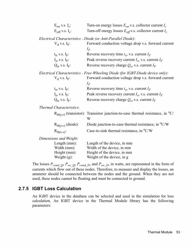
current IFtrr v.s. IF: Reverse recovery time trr v.s. current IFIrr v.s. IF: Peak reverse recovery current Irr v.s. current IFQrr v.s. IF: Reverse recovery charge Qrr v.s. current IF
Thermal Characteristics: Rth(j-c): Junction-to-case thermal resistance, in oC/WRth(c-s): Case-to-sink thermal resistance, in oC/W
Dimensions and Weight: Length (mm): Length of the device, in mmWidth (mm): Width of the device, in mmHeight (mm): Height of the device, in mmWeight (g): Weight of the device, in g
The losses Pcond and Psw, in watts, are represented in the form of currents which flowout of these nodes. Therefore, to measure and display the losses, an ammeter should beconnected between the Pcond or Psw node and the ground. When they are not used, thesetwo nodes cannot be floating, and must be connected to ground.
2.7.3 Diode Loss CalculationA diode device in the database can be selected and used in the simulation for losscalculation. A diode in the Thermal Module library has the following parameters:
Attributes:
The parameter Frequency refers to the frequency under which the losses are calculated.For example, if the device operates at the switching frequency of 10 kHz, and the
Parameters Description
Device The specific device selected from the device database
Frequency Frequency, in Hz, under which the losses are calculated
Pcond Calibration Factor
The calibration factor Kcond of the conduction losses Pcond
Psw Calibration Factor The calibration factor Ksw of the switching losses Psw
Thermal Module 49

50
parameter Frequency is also set to 10 kHz, the losses will be the values for oneswitching period. However, if the parameter Frequency is set to 60 Hz, then the losseswill be the value for a period of 60 Hz.
The parameter Pcond Calibration Factor is the correction factor for the conductionlosses. For the example, if the calculated conduction losses before the correction isPcond_cal, then
Pcond = Kcond * Pcond_cal
Similarly, the parameter Psw Calibration Factor is the correction factor for theswitching losses. For the example, if the calculated switching losses before thecorrection is Psw_cal, then
Psw = Ksw * Psw_cal
Conduction Losses:
The diode conduction losses is calculated as:
Conduction Losses = Vd * IF
where Vd is the diode voltage drop, and IF is the diode forward current.
Switching Losses:
In calculating the switching losses, the diode turn-on losses are neglected and are notconsidered. The diode turn-off losses due to the reverse recovery is calculated as:
Turn-off Losses = 1/4 * Qrr * VR * f
where Qrr is the reverse recovery charge, VR is the reverse blocking voltage, and f is thefrequency as defined in the input parameter Frequency. The reverse recovery charge Qrris defined as:
Qrr = 1/2 * trr * Irr
Whenever Qrr is given in the device database, the losses will be calculated based on Qrr.If Qrr is not given, the losses will be calculated based on trr and Irr. If both are not given,the losses will be treated as 0.
Example: Diode Loss Calculation The circuit below shows a sample circuit that uses the Powerex’s discrete diodeCS240650 (600V, 50A). The conduction losses and the switching losses are measuredthrough two ammeters.
Power Circuit Components

Once the information of the losses is available, by building the thermal equivalentcircuit, the device junction temperature can be calculated. The circuit shows a thermalcircuit without considering the thermal transient.
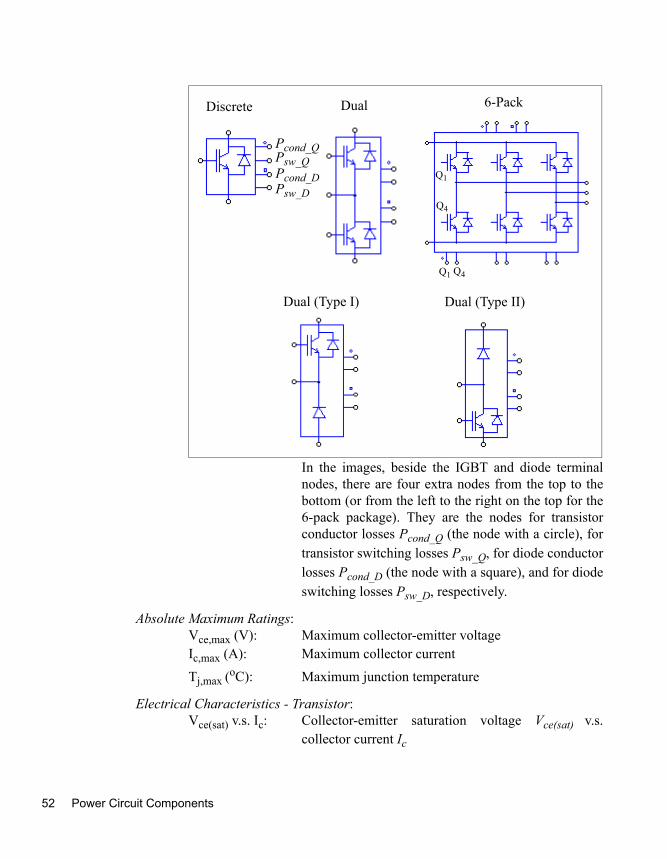
2.7.4 IGBT Device in the DatabaseAn IGBT device has three types of packages: discrete, dual, or 6-pack.
For the dual package, both the top and the bottom switches can be IGBT’s (full-bridgeconfiguration), or one of the switches is IGBT and the other is a free-wheeling diode(half-bridge configuration). For the half-bridge dual IGBT device, since the free-wheeling diode parameters can be different from these of the anti-parallel diode, thistype of device is referred to as the IGBT-Diode device, and is treated as a different typein the simulation. But for the convenience of discussion, both devices are referred to asthe IGBT devices here.
The following information is defined for an IGBT device in the database:
General Information: Manufacturer: Device manufacturePart Number: Manufacturer’s part numberPackage: It can be discrete, dual, or 6-pack, as shown in the
figure below:
Speed Sensor
Thermal Module 51
52
In the images, beside the IGBT and diode terminalnodes, there are four extra nodes from the top to thebottom (or from the left to the right on the top for the6-pack package). They are the nodes for transistorconductor losses Pcond_Q (the node with a circle), fortransistor switching losses Psw_Q, for diode conductorlosses Pcond_D (the node with a square), and for diodeswitching losses Psw_D, respectively.
Absolute Maximum Ratings: Vce,max (V): Maximum collector-emitter voltageIc,max (A): Maximum collector current
Tj,max (oC): Maximum junction temperature
Electrical Characteristics - Transistor: Vce(sat) v.s. Ic: Collector-emitter saturation voltage Vce(sat) v.s.
collector current Ic
Discrete Dual
Dual (Type I)
6-Pack
Psw_QPcond_Q
Psw_D
Pcond_D Q1
Q4
Q1 Q4
Dual (Type II)
Power Circuit Components
Eon v.s. Ic: Turn-on energy losses Eon v.s. collector current IcEoff v.s. Ic: Turn-off energy losses Eoff v.s. collector current Ic
Electrical Characteristics - Diode (or Anti-Parallel Diode): Vd v.s. IF: Forward conduction voltage drop v.s. forward current
IFtrr v.s. IF: Reverse recovery time trr v.s. current IFIrr v.s. IF: Peak reverse recovery current Irr v.s. current IFQrr v.s. IF: Reverse recovery charge Qrr v.s. current IF
Electrical Characteristics - Free-Wheeling Diode (for IGBT-Diode device only): Vd v.s. IF: Forward conduction voltage drop v.s. forward current
IFtrr v.s. IF: Reverse recovery time trr v.s. current IFIrr v.s. IF: Peak reverse recovery current Irr v.s. current IFQrr v.s. IF: Reverse recovery charge Qrr v.s. current IF
Thermal Characteristics: Rth(j-c) (transistor): Transistor junction-to-case thermal resistance, in oC/
WRth(j-c) (diode): Diode junction-to-case thermal resistance, in oC/WRth(c-s): Case-to-sink thermal resistance, in oC/W
Dimensions and Weight: Length (mm): Length of the device, in mmWidth (mm): Width of the device, in mmHeight (mm): Height of the device, in mmWeight (g): Weight of the device, in g
The losses Pcond_Q, Psw_Q, Pcond_D, and Psw_D, in watts, are represented in the form ofcurrents which flow out of these nodes. Therefore, to measure and display the losses, anammeter should be connected between the nodes and the ground. When they are notused, these nodes cannot be floating and must be connected to ground.
2.7.5 IGBT Loss CalculationAn IGBT device in the database can be selected and used in the simulation for losscalculation. An IGBT device in the Thermal Module library has the followingparameters:
Thermal Module 53

54
Attributes:
The parameter Frequency refers to the frequency under which the losses are calculated.For example, if the device operates at the switching frequency of 10 kHz, and theparameter Frequency is also set to 10 kHz, the losses will be the values for oneswitching period. However, if the parameter Frequency is set to 60 Hz, then the losseswill be the value for a period of 60 Hz.
The parameter Pcond_Q Calibration Factor is the correction factor for the transistorconduction losses. For the example, if the calculated conduction losses before thecorrection is Pcond_Q_cal, then
Pcond_Q = Kcond_Q * Pcond_Q_cal
Similarly, the parameter Psw_Q Calibration Factor is the correction factor for thetransistor switching losses. For the example, if the calculated switching losses before thecorrection is Psw_Q_cal, then
Psw_Q = Ksw_Q * Psw_Q_cal
Parameters Pcond_D Calibration Factor and Psw_D Calibration Factor work in the sameway, except that they are for the diode losses.
Conduction Losses:
The transistor conduction losses is calculated as:
Transistor Conduction Losses = Vce(sat) * Ic
Parameters Description
Device The specific device selected from the device database
Frequency Frequency, in Hz, under which the losses are calculated
Pcond_Q Calibration Factor
The calibration factor Kcond_Q of the transistor conduction losses Pcond_Q
Psw_Q Calibration Factor
The calibration factor Ksw_Q of the transistor switching losses Psw_Q
Pcond_D Calibration Factor
The calibration factor Kcond_D of the diode conduction losses Pcond_D
Psw_D Calibration Factor
The calibration factor Ksw_D of the diode switching losses Psw_D
Power Circuit Components

where Vce(sat) is the transistor collector-emitter saturation voltage, and Ic is the collectcurrent.
Switching Losses:
The transistor turn-on losses is calculated as:
Transistor Turn-on Losses = Eon * f
where Eon is the transistor turn-on energy losses, and f is the frequency as defined in theinput parameter Frequency.
The transistor turn-off losses is calculated as:
Transistor Turn-off Losses = Eoff * f
where Eoff is the transistor turn-off energy losses.
The loss calculation for the anti-parallel diode or free-wheeling diode is the same asdescribed in the section for the diode device.
Example: IGBT Loss Calculation The circuit below shows a sample circuit that uses Powerex’s 6-pack IGBT moduleCM100TU-12H (600V, 100A). The conduction losses and the switching losses of thetransistors and the diodes are added separately, and a thermal equivalent circuit isprovided to calculate the temperature raise.
With the Thermal Module, users can quickly check the thermal performance of a deviceunder different operating conditions, and compare the devices of different manufactures.
Thermal Module 55

56
2.7.6 MOSFET Device in the DatabaseThe following information is defined for a MOSFET device in the database:
General Information: Manufacturer: Device manufacturePart Number: Manufacturer’s part numberPackage: It can be discrete, dual, or 6-pack, as shown in the
figure below:
Power Circuit Components

In the images, beside the MOSFET and diodeterminal nodes, there are four extra nodes from thetop to the bottom (or from the left to the right on thetop for the 6-pack package). They are the node fortransistor conductor losses Pcond_Q (the node with acircle), for transistor switching losses Psw_Q, fordiode conductor losses Pcond_D (the node with asquare), and for diode switching losses Psw_D,respectively.
Absolute Maximum Ratings: VDS,max (V): Maximum drain-to-source voltageID,max (A): Maximum continuous drain current
Tj,max (oC): Maximum junction temperature
Electrical Characteristics - Transistor: RDS(on) (ohm): Static drain-to-source on-resistance (test conditions:
gate-to-source voltage VGS, in V, and drain current ID,in A)
VGS(th) (V): Gate threshold voltage VGS(th) (test condition: draincurrent ID, in A)
gfs (S): Forward transconductance gfs (test conditions: drain-to-source voltage VDS, in V, and drain current ID, inA)
tr (ns) and tf (ns): Rise time tr and fall time tf (test conditions: drain-to-source voltage VDS, in V; drain current ID, in A; and
Discrete Dual 6-Pack
Psw_QPcond_Q
Psw_D
Pcond_D Q1
Q4
Q1 Q4
(n-channel)
(p-channel)
Thermal Module 57

58
gate resistance Rg, in ohm)Qg, Qgs, and Qgd: Total gate charge Qg, gate-to-source charge Qgs, and
gate-to-drain ("Miller") charge Qgd, respectively, allin nC (test conditions: drain-to-source voltage VDS, inV; gate-to-source voltage VDS, in V; and drain currentID, in A)
Ciss, Coss, and Crss: Input capacitance Ciss, output capacitance Coss, andreverse transfer capacitance Crss, respectively, all inpF (test conditions: drain-to-source voltage VDS, in V;gate-to-source voltage VDS, in V; and test frequency,in MHz)
Electrical Characteristics - Diode: Vd v.s. IF: Forward conduction voltage drop Vd v.s. forward
current IFtrr and Qrr: Reverse recovery time trr, in ns, and reverse recovery
charge Qrr, in uC (test conditions: forward current IF,in A; rate of change of the current di/dt, in A/us, andjunction temperature Tj, in oC)
Thermal Characteristics: Rth(j-c): Junction-to-case thermal resistance, in oC/WRth(c-s): Case-to-sink thermal resistance, in oC/W
Dimensions and Weight: Length (mm): Length of the device, in mmWidth (mm): Width of the device, in mmHeight (mm): Height of the device, in mmWeight (g): Weight of the device, in g
The losses Pcond_Q, Psw_Q, Pcond_D, and Psw_D, in watts, are represented in the form ofcurrents which flow out of these nodes. Therefore, to measure and display the losses, anammeter should be connected between the nodes and the ground. When they are notused, these nodes cannot be floating and must be connected to ground.
2.7.7 MOSFET Loss CalculationA MOSFET device in the database can be selected and used in the simulation for losscalculation. A MOSFET in the Thermal Module library has the following parameters:
Power Circuit Components

Attributes:
The parameter Frequency refers to the frequency under which the losses are calculated.For example, if the device operates at the switching frequency of 10 kHz, and theparameter Frequency is also set to 10 kHz, the losses will be the values for oneswitching period. However, if the parameter Frequency is set to 60 Hz, then the losseswill be the value for a period of 60 Hz.
The parameter Pcond_Q Calibration Factor is the correction factor for the transistorconduction losses. For the example, if the calculated conduction losses before thecorrection is Pcond_Q_cal, then
Pcond_Q = Kcond_Q * Pcond_Q_cal
Parameters Description
Device The specific device selected from the device database
Frequency Frequency, in Hz, under which the losses are calculated
VGG+ (upper level) Upper level of the gate source voltage, in V
VGG- (lower level) Lower level of the gate source voltage, in V
Rg_on (turn-on) Gate resistance during turn-on
Rg_off (turn-off) Gate resistance during turn-off. In most cases, the turn-on gate resistance Rg_on and the turn-off gate resistance Rg_off are identical.
RDS(on) Calibration Factor
The calibration factor of the on-state resistance RDS(on)
gfs Calibration Factor The calibration factor of the forward transconductance gfs
Pcond_Q Calibration Factor
The calibration factor Kcond_Q of the transistor conduction losses Pcond_Q
Psw_Q Calibration Factor
The calibration factor Ksw_Q of the transistor switching losses Psw_Q
Pcond_D Calibration Factor
The calibration factor Kcond_D of the diode conduction losses Pcond_D
Psw_D Calibration Factor
The calibration factor Ksw_D of the diode switching losses Psw_D
Thermal Module 59

60
Similarly, the parameter Psw_Q Calibration Factor is the correction factor for thetransistor switching losses. For the example, if the calculated switching losses before thecorrection is Psw_Q_cal, then
Psw_Q = Ksw_Q * Psw_Q_cal
Parameters Pcond_D Calibration Factor and Psw_D Calibration Factor work in the sameway. except that they are for the diode losses.
Conduction Losses:
The transistor conduction losses is calculated as:
Conduction Losses = ID2 * RDS(on)
where ID is the drain current, and RDS(on) is the static on-resistance.
Switching Losses:
The transistor turn-on losses is calculated as:
Transistor Turn-on Losses = Eon * f
where Eon is the transistor turn-on energy losses, and f is the frequency as defined in theinput parameter Frequency.
The transistor turn-off losses is calculated as:
Transistor Turn-off Losses = Eoff * f
where Eoff is the transistor turn-off energy losses. The energy losses Eon and Eoff arecalculated based on the information of the gate current, input/output/reverse transfercapacitances, and gate charges of the MOSFET devices.
The loss calculation for the anti-parallel diode or free-wheeling diode is the same asdescribed in the diode device section.
Power Circuit Components

2.8 Motor Drive ModuleThe Motor Drive Module is an add-on module to the basic PSIM program. It providesmachine models and mechanical load models for motor drive system studies.
The Motor Drive Module includes electric machines as described in this section, andmechanical elements and speed/torque/position sensors as described in Section 2.11.
2.8.1 Reference Direction of Mechanical SystemsIn a motor drive system, in order to formulate equations for the mechanical system, aposition notation needs to be defined. Take the following motor drive system as anexample:
The system consists of two induction machines, IM1 and IM2, connected back-to-back.One operates as a motor, and the other as a generator. From the point of view of the firstmachine IM1, the mechanical equation can be written as:
where J1 and J2 are the moment of inertia, and Tem1 and Tem2 are the developed torquesof the machine IM1 and IM2, respectively.
From the point of view of the second machine IM2, however, the mechanical equationcan be written as:
These two equations are equally valid, but will produce opposite mechanical speed.
In order to avoid this ambiguity, in PSIM, the concept "reference direction" is used inthe mechanical system so that the mechanical equation can be uniquely defined.
In a mechanical system, one element is designated as the master unit (this element isconsidered to operate in the master mode), and the rest of the elements are in the slave
J1 J2+( )dωm
dt----------⋅ Tem1 Tem2–=
J1 J2+( )dωm
dt----------⋅ Tem2 Tem1–=
Motor Drive Module 61

62
mode. Elements that can be master units are: Electric machines, mechanical-to-electrical interface blocks, gear boxes, and devices modeled by Power ModelingBlocks.
The master unit defines the reference direction of the mechanical system. The directionis define as the direction from the shaft node of the master unit, along the shaft, to therest of the mechanical system.
Once the reference direction of the mechanical system is defined, the speed and torquereference of the mechanical system can be defined. For example, if we use the right-hand method, with the thumb pointing in the reference direction of the mechanicalsystem, by rotating the right hand, the fingers will point to the positive direction of thespeed and the torque.
Moreover, each mechanical element has its own reference direction. The followingdiagram shows the reference direction of each mechanical element, as indicated by thearrow:
The reference direction of each element and the reference direction of the overallmechanical system determine how the element interacts with the mechanical system.
For example, if the reference direction of a machine is along the same direction as thereference direction of the mechanical system, the developed torque of the machine willcontribute to the shaft rotation in the positive direction. However, if the referencedirection of the machine is opposite to that of the mechanical system, the developedtorque will contribute to the shaft rotation in the negative direction.
In the two-machine example above, using the notation of the "reference direction", if wedefine the machine IM1 as the master unit, the reference direction of the overallmechanical system will be from left to right, as shown below. Based on this direction,the machine IM1 will be along the reference direction, and the machine IM2 will be
Machines:
Mechanical Loads:
Speed Sensor: Torque Sensor: Gear Box: Mechanical-ElectricalInterface Block:
Encoders:
Power Circuit Components

opposite to the reference direction. This leads to the equivalent circuit of the mechanicalsystem as shown on the right.
Similarly, if we define the machine IM2 as the master unit, the reference direction of theoverall mechanical system will be from right to left, as shown below. Based on thisdirection, the machine IM1 will be opposite to the reference direction, and the machineIM2 will be along the reference direction. This leads to the equivalent circuit of themechanical system as shown on the right.
The following shows another mechanical system with sensors and loads connected indifferent ways.
Master Unit
Reference direction
Equivalent Circuit
(J1+J2)*dWm/dt = Tem1 - Tem2
Master Unit
Reference direction
Equivalent Circuit
(J1+J2)*dWm/dt = Tem2 - Tem1
Master Reference direction of the mechanical system
Load 1 Load 2SpeedSensor 1
TorqueSensor 1
Speed TorqueSensor 2 Sensor 2TL2TL1
Unit
Motor Drive Module 63

64
In this mechanical system, the machine on the left is the master unit. The referencedirection of the mechanical system is from left to the right along the mechanical shaft.Comparing this direction with the reference direction of each element, Load 1, SpeedSensor 1, and Torque Sensor 1, will be along the reference direction, and Load 2, SpeedSensor 2, and Torque Sensor 2 will be opposite to the reference direction of themechanical system.
Therefore, if the speed of the machine is positive, Speed Sensor 1 reading will bepositive, and Speed Sensor 2 reading will be negative.
Similarly, the two constant-torque mechanical loads, with the amplitudes of TL1 andTL2, interact with the machine in different ways. Load 1 is along the reference direction,and the loading torque of Load 1 to the master machine will be TL1. On the other hand,Load 2 is opposite to the reference direction, and the loading torque of Load 2 to themachine will be -TL2.
2.8.2 DC MachineThe image and parameters of a dc machine are as follows:
Image:
Attributes:
Parameters Description
Ra (armature) Armature winding resistance, in Ohm
La (armature) Armature winding inductance, in H
Rf (field) Field winding resistance, in Ohm
Lf (field) Field winding inductance, in H
+
-
+
-
ArmatureWinding
FieldWinding
Shaft Node
Power Circuit Components

When the torque flag is set to 1, the internal torque generated by the machine will besaved to the output file for display.
For more details on the definition and use of the master/slave flag, refer to Section 2.8.1.
The operation of a dc machine is described by the following equations:
where vt, vf, ia, and if are the armature and field winding voltage and current,respectively; Ea is the back emf, ωm is the mechanical speed in rad./sec., Tem is theinternal developed torque, and TL is the load torque. The back emf and the internaltorque can also be expressed as:
where Laf is the mutual inductance between the armature and the field windings. It can
Moment of Inertia Moment of inertia of the machine, in kg*m2
Vt (rated) Rated armature terminal voltage, in V
Ia (rated) Rated armature current, in A
n (rated) Rated mechanical speed, in rpm
If (rated) Rated field current, in A
Torque Flag Output flag for internal torque Tem
Master/Slave Flag The master/slave flag of the machine
vt Ea ia Ra Ladia
dt-------+⋅+=
vf if Rf Lfdif
dt------+⋅=
Ea k φ ωm⋅ ⋅=
Tem k φ ia⋅ ⋅=
Jdωm
dt----------⋅ Tem TL–=
Ea Laf if ωm⋅ ⋅=
Tem Laf if ia⋅ ⋅=
Motor Drive Module 65

66
be calculated based on the rated operating conditions as:
Note that the dc machine model assumes magnetic linearity. Saturation is notconsidered.
Example: A DC Motor with a Constant-Torque Load The circuit below shows a shunt-excited dc motor with a constant-torque load TL. Sincethe load is along the reference direction of the mechanical system, the loading torque tothe machine is TL. Also, the speed sensor is along the reference direction. It will give apositive output for a positive speed.
The simulation waveforms of the armature current and the speed are shown on the right.
2.8.3 Induction MachineLinear and nonlinear models are provided for squirrel-cage and wound-rotor inductionmachines. The linear model is further divided into general type and symmetrical type.This section describes the linear models.
Four linear models are provided:
- Symmetrical 3-phase squirrel-cage induction machine- General 3-phase squirrel-cage induction machine - Symmetrical 3-phase wound-rotor induction machine - General 3-phase wound-rotor induction machine
The images and parameters are shown as follows.
LafVt Ia Ra⋅–( )
If ωm⋅------------------------------=
Speed Sensor
Constant-
LoadTorque
Speed (in rpm)
Armature current
Power Circuit Components

Images:
Attributes:
Parameters Description
Rs (stator) Stator winding resistance, in Ohm
Ls (stator) Stator winding leakage inductance, in H
Rr (rotor) Rotor winding resistance, in Ohm
Lr (rotor) Rotor winding leakage inductance, in H
Lm (magnetizing) Magnetizing inductance, in H
Ns/Nr Turns Ratio Stator and rotor winding turns ratio (for wound-rotor machine only)
No. of Poles Number of poles P of the machine (an even integer)
Moment of Inertia Moment of inertia J of the machine, in kg*m2
Torque Flag Output flag for internal torque Tem
Master/Slave Flag Master/slave flag of the machine
as+as-bs+bs-cs+cs-
Squirrel-cage Squirrel-cage Squirrel-cage
as
bs
cs
ns
as
bs
cs
as
bs
cs
ns
nr
as+as-bs+bs-cs+cs-
ar br cr ar+ br+ cr+ar- br- cr-
Wound-rotorWound-rotor
(with neutral) (unconnected)
(unconnected)
Motor Drive Module 67

68
All the parameters are referred to the stator side.
For more details on the definition and use of the master/slave flag, refer to Section 2.8.1.
The models of the squirrel-cage induction machine with and without the neutral are thesame internally.
The operation of a 3-phase induction machine is described by the following equations:
where
For squirrel-cage machines, va,r = vb,r = vc,r= 0. The parameter matrices are defined as:
vabc s, Rs iabc s, Lsddt----- iabc s, Msr
ddt-----⋅ iabc r,+⋅+⋅=
vabc r, Rr iabc r, Lrddt-----⋅ iabc r, Msr
T ddt-----⋅ iabc s,++⋅=
vabc s,
va s,
vb s,
vc s,
= vabc r,
va r,
vb r,
vc r,
= iabc s,
ia s,
ib s,
ic s,
= iabc r,
ia r,
ib r,
ic r,
=
Rs
Rs 0 00 Rs 00 0 Rs
= Rr
Rr 0 00 Rr 00 0 Rr
=
Ls
Ls Msr+Msr
2--------–
Msr
2--------–
Msr
2--------– Ls Msr+
Msr
2--------–
Msr
2--------–
Msr
2--------– Ls Msr+
= Lr
Lr Msr+Msr
2--------–
Msr
2--------–
Msr
2--------– Lr Msr+
Msr
2--------–
Msr
2--------–
Msr
2--------– Lr Msr+
=
Msr Msr
θcos θ 2π3
------+⎝ ⎠⎛ ⎞cos θ 2π
3------–⎝ ⎠
⎛ ⎞cos
θ 2π3
------–⎝ ⎠⎛ ⎞cos θcos θ 2π
3------+⎝ ⎠
⎛ ⎞cos
θ 2π3
------+⎝ ⎠⎛ ⎞cos θ 2π
3------–⎝ ⎠
⎛ ⎞cos θcos
⋅=
Power Circuit Components

where Msr is the mutual inductance between the stator and rotor windings, and θ is themechanical angle. The mutual inductance is related to the magnetizing inductance as:
The mechanical equation is expressed as:
where the developed torque Tem is defined as:
For a symmetrical squirrel-cage induction machine, the steady state equivalent circuit isshown below. In the figure, s is the slip.
Example: A VSI Induction Motor Drive System The figure below shows an open-loop induction motor drive system. The motor has 6poles and is fed by a voltage source inverter with sinusoidal PWM. The dc bus is fedthrough a diode bridge.
The simulation waveforms of the mechanical speed (in rpm), developed torque Tem andload torque Tload, and 3-phase input currents show the start-up transient.
Lm32---Msr=
Jdωm
dt----------⋅ Tem TL–=
Tem P iabc s,
T ddθ------ Msr iabc r,⋅ ⋅ ⋅=
Rs RrLs Lr
Lm Rr(1-s)/s
Motor Drive Module 69

70
2.8.4 Induction Machine with SaturationTwo models of induction machines with saturation are provided:
- 3-phase squirrel-cage induction machine - 3-phase wound-rotor induction machine
Images:
InductionMotorBridge
Diode
VSI
SpeedSensor
TorqueSensor
SPWM
Speed
Tem
Tload
3-phase currents
as+as-bs+bs-cs+cs-
as+as-bs+bs-cs+cs-
ar+ br+ cr+ar- br- cr-
Wound-rotor (nonlinear)Squirrel-cage (nonlinear)
Power Circuit Components

r
Attributes:
All the parameters are referred to the stator side.
For more details on the definition and use of the master/slave flag, refer to Section 2.8.1.
The operation of a 3-phase induction machine with saturation is described by thefollowing equations:
where
Parameters Description
Rs (stator) Stator winding resistance, in Ohm
Ls (stator) Stator winding leakage inductance, in H
Rr (rotor) Rotor winding resistance, in Ohm
Lr (rotor) Rotor winding leakage inductance, in H
Ns/Nr Turns Ratio Stator and rotor winding turns ratio (for wound-rotor machine only)
No. of Poles Number of poles P of the machine (an even integer)
Moment of Inertia Moment of inertia J of the machine, in kg*m2
Torque Flag Output flag for internal torque Tem
Master/Slave Flag Master/slave flag of the machine
Im v.s. Lm (Im1,Lm1) ... Characteristics of the magnetizing current Im versus the magnetizing inductance [(Im1,Lm1) (Im2,Lm2) ...]
vabc s, Rs iabc s, Lsddt----- iabc s,
ddt----- λabc s,+⋅+⋅=
vabc r, Rr iabc r, Lrddt-----⋅ iabc r,
ddt----- λabc r,++⋅=
λabc s, Msr
1 12---– 1
2---–
12---– 1 1
2---–
12---– 1
2---– 1
iabc s,⋅ ⋅ Msr+
θcos θ 2π3
------+⎝ ⎠⎛ ⎞cos θ 2π
3------–⎝ ⎠
⎛ ⎞cos
θ 2π3
------–⎝ ⎠⎛ ⎞cos θcos θ 2π
3------+⎝ ⎠
⎛ ⎞cos
θ 2π3
------+⎝ ⎠⎛ ⎞cos θ 2π
3------–⎝ ⎠
⎛ ⎞cos θcos
iabc,⋅=
Motor Drive Module 71

72
r
In this case, the inductance Msr is no longer constant, but a function of the magnetizingcurrent Im.
2.8.5 Brushless DC MachineA 3-phase brushless dc machine is a type of permanent magnet synchronous machinewith trapezoidal waveform back emf. It has 3-phase windings on the stator, andpermanent magnet on the rotor.
The image and parameters of the 3-phase brushless dc machine are shown as follows.
Image:
Attributes:
Parameters Description
R (stator resistance) Stator phase resistance R, in Ohm
L (stator self ind.) Stator phase self inductance L, in H
λabc s, Msr
θcos θ 2π3
------–⎝ ⎠⎛ ⎞cos θ 2π
3------+⎝ ⎠
⎛ ⎞cos
θ 2π3
------+⎝ ⎠⎛ ⎞cos θcos θ 2π
3------–⎝ ⎠
⎛ ⎞cos
θ 2π3
------–⎝ ⎠⎛ ⎞cos θ 2π
3------+⎝ ⎠
⎛ ⎞cos θcos
iabc s,⋅ ⋅ Msr+
1 12---– 1
2---–
12---– 1 1
2---–
12---– 1
2---– 1
iabc,⋅=
a
b
c
sa sb sc6-pulse Hall Effect Position Sensor
Shaft Node
n
Power Circuit Components

M (stator mutual ind.) Stator mutual inductance M, in HThe mutual inductance M is a negative value. Depending on the winding structure, the ratio between M and the stator self inductance L is normally between -1/3 and -1/2. If M is unknown, a reasonable value of M equal to -0.4*L can be used as the default value.
Vpk / krpm Peak line-to-line back emf constant, in V/krpm (mechanical speed)
Vrms / krpm RMS line-to-line back emf constant, in V/krpm (mechanical speed).The values of Vpk/krpm and Vrms/krpm should be available from the machine data sheet. If these values are not available, they can be obtained through experiments by operating the machine as a generator at 1000 rpm and measuring the peak and rms values of the line-to-line voltage.
No. of Poles P Number of poles P
Moment of Inertia Moment of inertia J of the machine, in kg*m2
Mech. Time Constant Mechanical time constant τmech
theta_0 (deg.) Initial rotor angle θr, in electrical deg.
The initial rotor angle is the rotor angle at t=0. The zero rotor angle position is defined as the position where Phase A back emf crosses zero (from negative to positive) under a positive rotation speed.
theta_advance (deg.) Position sensor advance angle θadvance, in electrical deg.
The advance angle is defined as such that, for a brushless dc machine with a 120o trapezoidal back emf waveform, if the advance angle is 0, the leading edge of the Phase A hall effect sensor signal will align with the intersection of the rising ramp and the flat-top of the back emf trapezoidal waveform.
Motor Drive Module 73

74
The node assignments of the image are: Nodes a, b, and c are the stator windingterminals for Phase A, B, and C, respectively. The stator windings are Y connected, andNode n is the neutral point. The shaft node is the connecting terminal for the mechanicalshaft. They are all power nodes and should be connected to the power circuit.
Node sa, sb, and sc are the outputs of the built-in 6-pulse hall effect position sensors forPhase A, B, and C, respectively. The sensor output is a bipolar commutation pulse (1, 0,and -1). The sensor output nodes are all control nodes and should be connected to thecontrol circuit.
For more details on the definition and use of the master/slave flag, refer to Section 2.8.1.
The equations of the 3-phase brushless dc machine are:
where va, vb, and vc are the phase voltages, ia, ib, and ic are the phase currents, R, L, andM are the stator phase resistance, self inductance, and mutual inductance, and Ea, Eb,and Ec are the back emf of Phase A, B, and C, respectively.
The back emf voltages are a function of the rotor mechanical speed ωm and the rotorelectrical angle θr, that is:
Conduction Pulse Width
Position sensor conduction pulse width, in electrical deg.Positive conduction pulse can turn on the upper switch and negative pulse can turn on the lower switch in a full bridge inverter. The conduction pulse width is 120 electrical deg. for 120o conduction mode.
Torque Flag Output flag for internal developed torque Tem
Master/Slave Flag Master/slave flag of the machine
va R ia L M–( )dia
dt------- Ea+⋅+⋅=
vb R ib L M–( )dib
dt------- Eb+⋅+⋅=
vc R ic L M–( )dic
dt------- Ec+⋅+⋅=
Ea ke_a ωm⋅=
Eb ke_b ωm⋅=
Power Circuit Components

The coefficients ke_a, ke_b, and ke_c are dependent on the rotor angle θr. In this model, anideal trapezoidal waveform profile is assumed, as shown below for Phase A. Also shownis the Phase A hall effect sensor signal Sa.
where Kpk is the peak trapezoidal value, in V/(rad./sec.), which is defined as:
. Given the values of Vpk/krpm and Vrms/krpm, the
angle α is determined automatically in PSIM.
The developed torque of the machine is:
The mechanical equations are:
where B is a coefficient, Tload is the load torque, and P is the no. of poles. Thecoefficient B is calculated from the moment of inertia J and the mechanical timeconstant τmech as below:
More Explanation on the Hall Effect Sensor:A hall effect position sensor consists of a set of hall switches and a set of triggermagnets.
Ec ke_c ωm⋅=
α
θr
ke_a
Kpk
-Kpk
180o
360o
Sa
KpkVpk krpm⁄
2------------------------- 1
1000 2π 60⁄⋅---------------------------------⋅=
Tem Ea ia Eb ib Ec ic⋅+⋅+⋅( ) ωm⁄=
Jdωm
dt----------⋅ Tem B ωm Tload–⋅–=
dθr
dt-------- P
2--- ωm⋅=
B Jτmech------------=
Motor Drive Module 75

76
The hall switch is a semiconductor switch (e.g. MOSFET or BJT) that opens or closeswhen the magnetic field is higher or lower than a certain threshold value. It is based onthe hall effect, which generates an emf proportional to the flux-density when the switchis carrying a current supplied by an external source. It is common to detect the emfusing a signal conditioning circuit integrated with the hall switch or mounted veryclosely to it. This provides a TTL-compatible pulse with sharp edges and high noiseimmunity for connection to the controller via a screened cable. For a three-phasebrushless dc motor, three hall switches are spaced 120 electrical deg. apart and aremounted on the stator frame.
The set of trigger magnets can be a separate set of magnets, or it can use the rotormagnets of the brushless motor. If the trigger magnets are separate, they should have thematched pole spacing (with respect to the rotor magnets), and should be mounted on theshaft in close proximity to the hall switches. If the trigger magnets use the rotor magnetsof the machine, the hall switches must be mounted close enough to the rotor magnets,where they can be energized by the leakage flux at the appropriate rotor positions.
Example: Start-Up of an Open-Loop Brushless DC Motor The figure below shows an open-loop brushless dc motor drive system. The motor is fedby a 3-phase voltage source inverter. The outputs of the motor hall effect positionsensors are used as the gatings signals for the inverter, resulting a 6-pulse operation.
The simulation waveforms show the start-up transient of the mechanical speed (in rpm),developed torque Tem, and 3-phase input currents.
Brushless DC Motor
Speed
Tem
3-phase currents
Power Circuit Components

Example: Brushless DC Motor with Speed FeedbackThe figure below shows a brushless dc motor drive system with speed feedback. Thespeed control is achieved by modulating sensor commutation pulses (Vgs for Phase A inthis case) with another high-frequency pulses (Vgfb for Phase A). The high-frequencypulse is generated from a dc current feedback loop.
The simulation waveforms show the reference and actual mechanical speed (in rpm),Phase A current, and signals Vgs and Vgfb. Note that Vgfb is divided by half for displaypurpose.
2.8.6 Synchronous Machine with External ExcitationThe structure of a conventional synchronous machine consists of three stator windings,one field winding on either a salient or cylindrical rotor, and an optional dampingwinding on the rotor.
Depending on the way the internal model interfaces with the external stator circuitry,there are two types of interface: one is the voltage-type interface, and the other is thecurrent-type interface. The model for the voltage-type interface consists of controlledvoltage sources on the stator side, and this model is suitable in situations where themachine operates as a generator and/or the stator external circuit is in series withinductive branches. On the other hand, The model for the current-type interface consistsof controlled current sources on the stator side, and this model is suitable in situationswhere the machine operates as a motor and/or the stator external circuit is in parallelwith capacitive branches.
Brushless DC Motor
Speed
Phase A current
VgsVgfb/2
Motor Drive Module 77

78
The image and parameters of the machine are shown as follows.
Image:
Attributes:
Parameters Description
Rs (stator) Stator winding resistance, in Ohm
Ls (stator) Stator leakage inductance, in H
Ldm (d-axis mag. ind.) d-axis magnetizing inductance, in H
Lqm (q-axis mag. ind.) q-axis magnetizing inductance, in H.
Rf (field) Field winding resistance, in Ohm
Lfl (field leakage ind.) Field winding leakage inductance, in H
Rdr (damping cage) Rotor damping cage d-axis resistance, in Ohm
Ldrl (damping cage) Rotor damping cage d-axis leakage inductance, in H
Rqr (damping cage) Rotor damping cage q-axis resistance, in Ohm
Lqrl (damping cage) Rotor damping cage q-axis leakage inductance, in H
Ns/Nf (effective) Stator-field winding effective turns ratio
Number of Poles P Number of Poles P
Moment of Inertia Moment of inertia J of the machine, in kg*m2
Torque Flag Output flag for internal developed torque Tem
Master/slave Flag Master/slave flag of the machine
a
b
c
Shaft Node
n
field-field+
Power Circuit Components

All the parameters are referred to the stator side.
For more details on the definition and use of the master/slave flag, refer to Section 2.8.1.
The equations of the synchronous machine can be expressed as follows:
where
and [λ] = [L]*[I]. The inductance matrix is defined as follows:
and
V R Iddt----- λ+⋅=
V va vb vc vf 0 0T
= I ia ib ic if idr iqr
T=
R diag Rs Rs Rs Rf Rdr Rqr= λ λa λb λc λf λdr λqr
T=
LL11 L12
L12
TL22
=
L11
Ls Lo L2 2θr( )cos+ +Lo
2-----– L2 2θr
2π3
------–⎝ ⎠⎛ ⎞cos+
Lo
2-----– L2 2θr
2π3
------+⎝ ⎠⎛ ⎞cos+
Lo
2-----– L2 2θr
2π3
------–⎝ ⎠⎛ ⎞cos+ Ls Lo L2 2θr
2π3
------+⎝ ⎠⎛ ⎞cos+ +
Lo
2-----– L2 2θr( )cos+
Lo
2-----– L2 2θr
2π3
------+⎝ ⎠⎛ ⎞cos+
Lo
2-----– L2 2θr( )cos+ Ls Lo L2 2θr
2π3
------–⎝ ⎠⎛ ⎞cos+ +
=
L12
Lsf 2θr( )cos Lsd 2θr( )cos L– sq 2θr( )sin
Lsf 2θr2π3
------–⎝ ⎠⎛ ⎞cos Lsd 2θr
2π3
------–⎝ ⎠⎛ ⎞cos L– sq 2θr
2π3
------–⎝ ⎠⎛ ⎞sin
Lsf 2θr2π3
------+⎝ ⎠⎛ ⎞cos Lsd 2θr
2π3
------+⎝ ⎠⎛ ⎞cos L– sq 2θr
2π3
------+⎝ ⎠⎛ ⎞sin
=
L22
Lf Lfdr 0Lfdr Ldr 0
0 0 Lqr
=
Motor Drive Module 79

80
where θr is the rotor angle.
The developed torque can be expressed as:
The mechanical equations are:
2.8.7 Permanent Magnet Synchronous MachineA 3-phase permanent magnet synchronous machine has 3-phase windings on the stator,and permanent magnet on the rotor. The difference between this machine and thebrushless dc machine is that the machine back emf is sinusoidal.
The image and parameters of the machine are shown as follows.
Image:
Attributes:
Parameters Description
Rs (stator resistance) Stator winding resistance, in Ohm
Ld (d-axis ind.) Stator d-axis inductance, in H
T P2--- I
ddθr-------- L I⋅ ⋅ ⋅=
Jdωm
dt----------⋅ Tem Tload–=
dθr
dt-------- P
2--- ωm⋅=
a
b
c
Shaft Node
n
Power Circuit Components

The node assignments of the image are: Nodes a, b, and c are the stator windingterminals for Phase a, b, and c, respectively. The stator windings are Y connected, andNode n is the neutral point. The shaft node is the connecting terminal for the mechanicalshaft. They are all power nodes and should be connected to the power circuit.
For more details on the definition and use of the master/slave flag, refer to Section 2.8.1.
The equations of the permanent-magnet synchronous machine are:
where va, vb, vc, and ia, ib, and ic, and λa, λb, λc are the stator phase voltages, currents,and flux linkages, respectively, and Rs is the stator phase resistance. The flux linkagesare further defined as:
Lq (q-axis ind.) Stator q-axis inductance, in H.The d-q coordinate is defined such that the d-axis passes through the center of the magnet, and the q-axis is in the middle between two magnets. The q-axis is leading the d-axis.
Vpk / krpm Peak line-to-line back emf constant, in V/krpm (mechanical speed).The value of Vpk/krpm should be available from the machine data sheet. If this data is not available, it can be obtained through an experiment by operating the machine as a generator at 1000 rpm and measuring the peak line-to-line voltage.
No. of Poles P Number of poles P
Moment of Inertia Moment of inertia J of the machine, in kg*m2
Mech. Time Constant Mechanical time constant τmech
Torque Flag Output flag for internal developed torque Tem
Master/slave Flag Master/slave flag of the machine
va
vb
vc
Rs 0 00 Rs 00 0 Rs
ia
ib
ic
ddt-----
λa
λb
λc
+⋅=
Motor Drive Module 81

82
where θr is the rotor electrical angle, and λpm is a coefficient which is defined as:
where P is the number of poles.
The stator self and mutual inductances are rotor position dependent, and are defined as:
where Ls is the stator leakage inductance. The d-axis and q-axis inductances areassociated with the above inductances as follows:
The developed torque can be expressed as:
λa
λb
λc
Laa Lab Lac
Lba Lbb Lbc
Lca Lcb Lcc
ia
ib
ic
λpm
θr( )cos
θr2π3
------–⎝ ⎠⎛ ⎞cos
θr2π3
------+⎝ ⎠⎛ ⎞cos
⋅+⋅=
λpm60 Vpk krpm⁄⋅
3 π P 1000⋅ ⋅ ⋅---------------------------------------=
Laa Ls Lo L2 2θr( )cos⋅+ +=
Lbb Ls Lo L2 2θr2π3
------+⎝ ⎠⎛ ⎞cos⋅+ +=
Lcc Ls Lo L2 2θr2π3
------–⎝ ⎠⎛ ⎞cos⋅+ +=
Lab LbaLo
2-----– L2 2θr
2π3
------–⎝ ⎠⎛ ⎞cos⋅+= =
Lac LcaLo
2-----– L2 2θr
2π3
------+⎝ ⎠⎛ ⎞cos⋅+= =
Lbc LcbLo
2-----– L2 2θr( )cos⋅+= =
Ld Ls32---Lo
32---L2+ +=
Lq Ls32---Lo
32---L2–+=
Power Circuit Components

The mechanical equations are:
where B is a coefficient, Tload is the load torque, and P is the no. of poles. Thecoefficient B is calculated from the moment of inertia J and the mechanical timeconstant τmech as below:
2.8.8 Permanent Magnet Synchronous Machine with SaturationA 3-phase PMSM machine with saturation differs from that of a linear 3-phase PMSMmachine in that the d-axis and q-axis magnetizing inductances Ldm and Lqm can beexpressed as a nonlinear function of the d-axis and q-axis currents in the lookup tableform.
The image and parameters of the machine are shown as follows.
Image:
TemP2--- L2 ia ib ic
2θr( )sin 2θr2π3
------–⎝ ⎠⎛ ⎞sin 2θr
2π3
------+⎝ ⎠⎛ ⎞sin
2θr2π3
------–⎝ ⎠⎛ ⎞sin 2θr
2π3
------+⎝ ⎠⎛ ⎞sin 2θr( )sin
2θr2π3
------+⎝ ⎠⎛ ⎞sin 2θr( )sin 2θr
2π3
------–⎝ ⎠⎛ ⎞sin
ia
ib
ic
⋅ ⋅ ⋅ –⋅=
P2--- λpm ia ib ic
θr( )sin
θr2π3
------–⎝ ⎠⎛ ⎞sin
θr2π3
------+⎝ ⎠⎛ ⎞sin
⋅ ⋅⋅=
Jdωm
dt----------⋅ Tem B ωm Tload–⋅–=
dθr
dt-------- P
2--- ωm⋅=
B Jτmech------------=
Motor Drive Module 83

84
Attributes:
Parameters Description
Rs (stator resistance) Stator winding resistance, in Ohm
Ls (stator leakage ind.) Stator d-axis inductance, in H
Vpk / krpm Peak line-to-line back emf constant, in V/krpm (mechanical speed).The value of Vpk/krpm should be available from the machine data sheet. If this data is not available, it can be obtained through an experiment by operating the machine as a generator at 1000 rpm and measuring the peak line-to-line voltage.
No. of Poles P Number of poles P
Moment of Inertia Moment of inertia J of the machine, in kg*m2
Mech. Time Constant Mechanical time constant τmech, in sec. It is associated with the friction coefficient B as: B = J / τmech.
Ld Lookup Table File File name of the lookup table for Ldm
Lq Lookup Table File File name of the lookup table for Lqm
dq Flag Flag for the lookup table. When the flag is 0, Ldm and Lqm are function of Id and Iq. When the flag is 1, Ldm and Lqm are function of the current magnitude Im and the angle.
Transformation Flag Flag for the transformation convention (see details below)
Torque Flag Output flag for internal developed torque Tem
Master/Slave Flag Master/slave flag of the machine
a
b
c
Shaft Node
n
Power Circuit Components

For more details on the definition and use of the master/slave flag, refer to Section 2.8.1.
The relationship between the d-axis/q-axis inductances Ld/Lq and the magnetizinginductances Ldm/Lqm is as follows:
where Ls is the stator leakage inductance. Since Ls is normally very small, Ld can beconsidered equivalent to Ldm, and Lq can be considered equivalent to Lqm.
The Transformation Flag defines the transformation convention between the abc frameand the dq frame. When the Transformation Flag is 0:
The current vector angle is in deg., and is from -180o to 180o.
When the Transformation Flag is 1:
The current vector angle is in deg., and is from 0o to 360o.
Ld Ls Ldm+=
Lq Ls Lqm+=
Id
Iq
23---
θr( )cos θr2π3
------–⎝ ⎠⎛ ⎞cos θr
2π3
------+⎝ ⎠⎛ ⎞cos
θr( )sin– θr2π3
------–⎝ ⎠⎛ ⎞sin– θr
2π3
------+⎝ ⎠⎛ ⎞sin–
ia
ib
ic
⋅ ⋅=
Im Id2 Iq
2+=
θm 2 Iq Id,( )atan=
Id
Iq
23---
θr( )cos θr2π3
------–⎝ ⎠⎛ ⎞cos θr
2π3
------+⎝ ⎠⎛ ⎞cos
θr( )sin– θr2π3
------–⎝ ⎠⎛ ⎞sin– θr
2π3
------+⎝ ⎠⎛ ⎞sin–
ia
ib
ic
⋅ ⋅=
Im23--- Id
2 Iq2+⋅=
θm 2 Id– Iq,( )atan=
Motor Drive Module 85

86
The Ldm and Lqm lookup tables have the following format:
m, nVr,1, Vr,2, ..., Vr,mVc,1, Vc,2, ..., Vc,nL1,1, L1,2, ..., L1,nL2,1, L2,2, ..., L2,n... ... ...Lm,1, Lm,2, ..., Lm,n
where m is the number of rows and n is the number of columns; Vr is the row vector andVc is the column vector; and Li,j is the Ldm or Lqm inductance value, in H, at Row i andColumn j. Note that Vectors Vr and Vc must be monotonically increasing.
If the input is between two points, interpolation is used to calculate the value. If theinput is less than the minimum or greater than the maximum value, the input will be setto be the same as the minimum or maximum value.
This PMSM model with saturation can also be used as the linear PMSM model if thelookup tables are defined such that Ldm and Lqm are linear function of Id and Iq.
The following shows an example of the lookup table:4,15-5.7155 -4.8990 -4.0825 -3.2660 -5.7155 -4.8990 -4.0825 -3.2660 -2.4495 -1.6330 -0.8165 0 0.8165 1.6330 2.4495 3.2660 4.0825 4.8990 5.7155 0.0109 0.0109 0.0107 0.0104 0.0102 0.0100 0.0098 0.0098 0.0098 0.0100 0.0102 0.0104 0.0107 0.0109 0.0109 0.0109 0.0109 0.0109 0.0106 0.0109 0.0106 0.0105 0.0105 0.0105 0.0106 0.0109 0.0106 0.0109 0.0109 0.0109 0.0109 0.0109 0.0109 0.0109 0.0111 0.0108 0.0106 0.0106 0.0106 0.0108 0.0111 0.0109 0.0109 0.0109 0.0109 0.0110 0.0110 0.0111 0.0110 0.0110 0.0109 0.0108 0.0107 0.0108 0.0109 0.0110 0.0110 0.0111 0.0110 0.0110
Power Circuit Components

2.8.9 Switched Reluctance MachineThe model of a 3-phase switched reluctance machine with 6 stator teeth and 4 rotor teethis provided. The images and parameters are shown as follows.
Image:
Attributes:
For more details on the definition and use of the master/slave flag, refer to Section 2.8.1.
The node assignments are: Nodes a+, a-, b+, b-, and c+, c- are the stator windingterminals for Phase a, b, and c, respectively. The shaft node is the connecting terminalfor the mechanical shaft. They are all power nodes and should be connected to thepower circuit.
Node c1, c2, c3, and c4 are the control signals for Phase a, b, and c, respectively. Thecontrol signal value is a logic value of either 1 (high) or 0 (low). Node θ is the
Parameters Description
Resistance Stator phase resistance R, in Ohm
Inductance Lmin Minimum phase inductance, in H
Inductance Lmax Maximum phase inductance, in H
θr Duration of the interval where the inductance increases, in deg.
Moment of Inertia Moment of inertia J of the machine, in kg*m2
Torque Flag Output flag for internal torque Tem
Master/Slave Flag Master/slave flag of the machine
a+
b+
c+
a-
b-
c-
c1 c2c3 c4 c1 c4 c1 c4
Phase a Phase b Phase c
Shaft Node
θ
Motor Drive Module 87
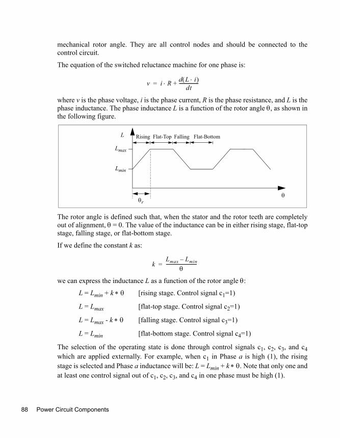
88
mechanical rotor angle. They are all control nodes and should be connected to thecontrol circuit.
The equation of the switched reluctance machine for one phase is:
where v is the phase voltage, i is the phase current, R is the phase resistance, and L is thephase inductance. The phase inductance L is a function of the rotor angle θ, as shown inthe following figure.
The rotor angle is defined such that, when the stator and the rotor teeth are completelyout of alignment, θ = 0. The value of the inductance can be in either rising stage, flat-topstage, falling stage, or flat-bottom stage.
If we define the constant k as:
we can express the inductance L as a function of the rotor angle θ:
L = Lmin + k ∗ θ [rising stage. Control signal c1=1)
L = Lmax [flat-top stage. Control signal c2=1)
L = Lmax - k ∗ θ [falling stage. Control signal c3=1)
L = Lmin [flat-bottom stage. Control signal c4=1)
The selection of the operating state is done through control signals c1, c2, c3, and c4which are applied externally. For example, when c1 in Phase a is high (1), the risingstage is selected and Phase a inductance will be: L = Lmin + k ∗ θ. Note that only one andat least one control signal out of c1, c2, c3, and c4 in one phase must be high (1).
v i R d L i⋅( )dt
-----------------+⋅=
θrθ
Lmin
Lmax
L Rising Flat-Top Falling Flat-Bottom
kLmax Lmin–
θ---------------------------=
Power Circuit Components

The developed torque of the machine per phase is:
Based on the inductance expression, we have the developed torque in each stage as:
Tem = i2*k / 2 [rising stage]
Tem = 0 [flat-top stage]
Tem = - i2*k / 2 [falling stage]
Tem = 0 [flat-bottom stage]
Note that saturation is not considered in this model.
Tem12--- i2 dL
dθ------⋅ ⋅=
Motor Drive Module 89

90
2.9 MagCoupler ModuleThe MagCoupler Module provides interface for co-simulation between PSIM and thesoftware JMAG. JMAG is an electromagnetic field analysis software for thedevelopment and design of electric machines, actuators, and other electrical andelectronic devices and components. With the MagCoupler Module, one can performpower electronics and control analysis and simulation, as well as the electromagneticfield analysis, all in one integral environment.
The MagCoupler Module includes the MagCoupler interface block as described in thissection, and mechanical elements and speed/torque/position sensors as described inSection 2.11.
To run the MagCoupler Module, the path of the JMAG directory must be included inPSIM so that PSIM can load JMAG DLL files. To set the JMAG directory path inPSIM, go to Options -> Set Path, and click on Add Folder to include the JMAGdirectory.
Also, the MagCoupler Module requires Microsoft Internet Explorer Version 6 or higher.It will not work with Internet Explorer Version 5.
Image:
Attributes:
Parameter Description
Link Table File The XML file that defines the interface between PSIM and JMAG. It has the .xml extension.
JMAG Input File The JCF input data file for JMAG. It has the .jcf extension. Note that the .xml file and the .jcf file must be in the same directory.
JMAG Case Text Comments for the JMAG circuit
IN Nodes Nodes that pass the values from PSIM to JMAG
Block with 4 inputs and 4 outputs
Power Circuit Components

The number of input and output nodes may vary, depending on the actual number ofinput/output nodes in a particular circuit.
The MagCoupler block accepts voltages, currents, and positions as inputs, and itprovides voltages, currents, positions, torques, and force as the outputs. In PSIM, theMagCoupler block is a power circuit element. The way it interfaces with the rest of thecircuit is that both the inputs and outputs are voltage signals (no electric current flowsinto the input node). To convert a branch current into a voltage signal, or vice versa, onecan use a current-controlled voltage source, or voltage-controlled current source.
The Link Table File, in XML format, defines the input/output interface and correspond-ing functions in JMAG. This file is generated automatically by JMAG. To locate thisfile, click on the browse button at the right of the edit field.
The JMAG Input File is the JCF input data file that is read by the JMAG solver. Thename is defined in the Link Table File.
Note that JCF input file .jcf must be in the same directory as the input link table file.xml. If any material database is used in JMAG, it should also be placed in the directoryof the .xml file. Also, the .xml file does not have to be in the same directory as theschematic file. However, if a .xml file with the same name is present in the schematicdirectory, PSIM will read the one in the schematic directory first.
The JMAG Case Text is a text identifying the specific JMAG circuit. It can be any textdescribing the JMAG circuit.
The IN Nodes are the nodes through which PSIM passes the values to JMAG. In theMagCoupler block image, the order of the input nodes is from the top to the bottom. Theorder can be changed by highlighting the node and click on the upper or down arrow.
The OUT Nodes are the nodes through which JMAG passes the values back to PSIM. Inthe MagCoupler block image, the order of the output nodes is from the top to thebottom. The order can be changed by highlighting the node and click on the upper ordown arrow.
By clicking on the Edit Image button, one can edit and customize the image of theMagCoupler block. Clicking on the Display File button will display the Link Table Filein the Microsoft Internet Explorer environment, and clicking on the Read File buttonwill read or re-load the Link Table File.
Set-up in JMAG and PSIM:Using the MagCoupler block, it is easy to set up the link between JMAG and PSIM forco-simulation. It involves two main steps: setting up the circuit in JMAG and generating
OUT Nodes Nodes that pass the values from JMAG to PSIM
MagCoupler Module 91

92
the link table file, and loading the link table file into PSIM.
An inductor example below is used to illustrate this process.
In the PSIM circuit of this example, the circuit on the left uses the built-in inductorelement from the PSIM library, and the circuit on the right has the inductor implementedin JMAG. In this case, the inductor is modelled as a controlled current source in PSIM.The voltage across the inductor is first converted to a node-to-ground voltage through avoltage-controlled voltage source, and the value is passed to the input node VL of theMagCoupler block. At each time step, PSIM calls JMAG functions which calculate theinductor current based on the voltage input. This current is then sent back to PSIM in thevoltage form, and is used to control the current source that represents the inductor.
In the JMAG circuit of this example, the voltage function (on the left side) receives thevoltage from PSIM, and through the current probe in series with the FEM coil, thecurrent is calculated and sent back to PSIM. The inductor structure in the JMAGenvironment is shown on the lower right.
Circuit in PSIM (file: inductor_jmag.sch)
Circuit and Structure in JMAG (file: inductor.jsp)
Power Circuit Components

The setup process of calling JMAG in PSIM through the MagCoupler block is asfollows.
In JMAG:- In the JMAG circuit, connect a voltage function to the right of the FEM coil.
Under Electrical Potential in the property window, choose Constant Value,and set Constant Value[V] to 0.
- Connect a current probe to the left of the FEM coil.
- Connect another voltage function to the left of the current probe (the circuitwill look like what is shown above). In the property window, chooseCooperates with an external circuit simulator.
- Highlight the inductor structure window. Go to the menu Conditions ->Create Conditions. From the Conditions List, highlight Coupled ExternalCircuit Simulator, and click Modify.
- On the Coupled External Circuit Simulator dialog window, there are twolists. The list on the right, called JMAG, contains all the functions that can beused to interface with PSIM. The list on the left, called External CircuitSimulator, contains the functions that are selected to interface with PSIM. Inthis case, there are two items in the JMAG list, one is the Voltage Function,and the other is the Current Probe.
- Highlight the Voltage Function, and click on the <- button to move the itemfrom the list on the right to the list on the left. Repeat the same step to theCurrent Probe. Now both items should appear in the list on the left.
- Highlight the Voltage Function, and change the terminal name to VL. Also,change the Current Probe terminal name to iL. Close the dialog window.
- Go to the menu File -> Export and select JCF.... With the JCF file namedefined as "inductor", the JCF file "inductor.jcf" and the link table file"inductor_csl.xml" will be generated.
- Copy the JCF file "inductor.jcf" and the link table file "inductor_csl.xml" to thefolder containing the PSIM schematic file "inductor_jmag.sch". Rename thelink table file to "inductor_jmag.xml". Note that the XML file does not have tobe renamed, and both the JCF and XML files do not have to be moved to thefolder of the schematic file. They are done here for the simplicity of filemanagement
In PSIM:- After the rest of the power circuit is created, go to Elements -> Power ->
MagCoupler Module 93

94
MagCoupler Module, and select MagCoupler Block. Place the block on theschematic.
- Double click on the MagCoupler block to bring out the property window. click
on the browser button next to the Link Table File edit field to locate andselect the file "inductor_jmag.xml". After the file is read, the property windowwill display the IN node VL and the OUT node iL.
- Connect the MagCouple block to the rest of the circuit in the schematic.
The setup is now complete and the simulation is ready to run.
Power Circuit Components

2.10 MagCoupler-RT ModuleThe MagCoupler-RT Module provides interface between PSIM and JMAG-RT datafiles. JMAG-RT is another way of modeling electromagnetic devices. The JMAG-RTdata files are obtained by running the JMAG simulation in advance, and are stored in alookup table form. During the PSIM simulation, JMAG is no longer needed, and PSIMinterfaces directly with the JMAG-RT data.
The biggest advantage of JMAG-RT is that, since the JMAG-RT data files are obtainedfrom the JMAG dynamic simulation, the accuracy of the JMAG-RT model iscomparable to that of a JMAG dynamic model. However, since JMAG is not involvedin the PSIM simulation, the PSIM simulation is significantly faster.
The MagCoupler Module includes the MagCoupler-RT blocks as described in thissection, and mechanical elements and speed/torque/position sensors as described inSection 2.11.
Images:
Attributes:
Parameter Description
Netlist XML File The XML file that defines the interface between PSIM and JMAG-RT. It has the .xml extension.
JMAG-RT Input File The JMAG-RT data file. It has the .rtt extension. Note that the .xml file and the .rtt file must be in the same directory.
JMAG Case Text Comments for the JMAG-RT circuit
Terminal Names Terminal names of the block
MagCoupler-RT BlockMagCoupler-RT PMSM BlockA B C A+ A- B+ B- C+ C-
M+M- M+
M-
MagCoupler-RT Module 95

96
In the MagCoupler-RT block images, the electric nodes (such as A, B, C, A+, A-, B+, B-, C+, and C-, as shown above) are placed at the top of the block, arranged from the leftto the right. The rotor shaft nodes are placed on the left and right of the block, with thefirst shaft node (such as M+ as shown above) on the right, and the second shaft node(such as M-) on the left.
The electric nodes and rotor shaft nodes, as well as the rest of the interface betweenPSIM and the JMAG-RT data files, are defined in the JMAG-RT Input File. This file isin XML format, and is generated by the JMAG-RT Manager. To specify this file, clickon the browse button at the right of the edit field.
The JMAG-RT Input File is the JMAG-RT data file for the device modeled. The file hasthe .rtt extension and is defined in the JMAG-RT Input File. Note that the .rtt file and the.xml file must be in the same directory.
The JMAG Case Text is a text identifying the specific JMAG-RT study case. It can beany text.
The Terminal Names are the names of the interface nodes. The nodes on the top of theblock are the power circuit nodes, and the nodes on the left and right of the blocks arethe mechanical shaft nodes.
Example: A PMSM motor drive system with PMSM modeled in JMAG-RTThe figure below shows a permanent-magnet synchronous motor (PMSM) drivesystem, with the PMSM modeled in JMAG-RT.
The figure below shows the property window of the MagCoupler-RT PMSM block. The.xml file in this example defines three electric nodes (Nodes U, V, and W), and two rotorshaft nodes (Nodes shaft+ and shaft-). The shaft nodes can be connected directly to
Power Circuit Components

other mechanical elements in the PSIM library, as shown in this case.
Besides the information of the .rtt file and the terminal names, the property window alsoshows a set of parameters that allow users to modify the values of selected variables inthe JMAG-RT data file. The last five parameters are the flags that, when set to 1, willdisplay the currents, back emf, as well as the rotor angle, speed, and the developedtorque of the machine. For definitions and the usage of these parameters, please consultthe relevant JMAG-RT document.
MagCoupler-RT Module 97

98
2.11 Mechanical Elements and SensorsThis section describes elements that are shared by Motor Drive Module, MagCouplerModule, and MagCoupler-RT Module. The elements include mechanical loads, gearboxes, mechanical coupling blocks, mechanical-electrical interface blocks, and variousspeed/torque/position sensors.
2.11.1 Mechanical LoadsSeveral mechanical load models are provided: constant-torque, constant-power,constant-speed, general-type, and externally controlled loads.
2.11.1.1 Constant-Torque LoadThe image of a constant-torque load is:
Image:
Attributes:
If the reference direction of a mechanical system enters the dotted terminal, the load isalong the reference direction, and the loading torque to the master machine is Tconst.Otherwise the loading torque will be -Tconst. See Section 2.6.1 for more detailedexplanation on the reference direction.
A constant-torque load is expressed as:
The torque does not depend on the speed direction.
Parameters Description
Constant Torque Torque constant Tconst, in N*m
Moment of Inertia Moment of inertia of the load, in kg*m2
TL Tconst=
Power Circuit Components

2.11.1.2 Constant-Power LoadThe image of a constant-power load is:
Image:
Attributes:
The torque-speed curve of a constant-power load is shown below:
When the mechanical speed is less than the base speed nbase, the load torque is:
When the mechanical speed is above the base speed, the load torque is:
where P = Tmax*ωbase and ωbase = 2π∗nbase/60. The mechanical speed ωm is in rad./sec.
Parameters Description
Maximum Torque Maximum torque Tmax of the load, in N*m
Base Speed Base speed nbase of the load, in rpm
Moment of Inertia Moment of inertia of the load, in kg*m2
Speed (rpm)
Tmax
0
Torque
(N*m)
nbase
TL Tmax=
TLP
ωm----------=
Mechanical Elements and Sensors 99

10
2.11.1.3 Constant-Speed LoadThe image of a constant-torque load is:
Image:
Attributes:
A constant-speed mechanical load defines the speed of a mechanical system, and thespeed will remain constant, as defined by the speed constant.
2.11.1.4 General-Type LoadThe image of a general-type mechanical load is as follows.
Image:
Attributes:
A general-type load is expressed as:
Parameters Description
Constant Speed (rpm) Speed constant, in rpm
Moment of Inertia Moment of inertia of the load, in kg*m2
Parameters Description
Tc Constant torque term
k1 (coefficient) Coefficient for the linear term
k2 (coefficient) Coefficient for the quadratic term
k3 (coefficient) Coefficient for the cubic term
Moment of Inertia Moment of inertia of the load, in kg*m2
0 Power Circuit Components

where ωm is the mechanical speed in rad./sec.
Note that the torque of the general-type load is dependent on the speed direction.
2.11.1.5 Externally-Controlled LoadAn externally-controlled mechanical load is used to define a load of an arbitrary loadprofile.
Image:
Attributes:
The value of the mechanical load is defined by the voltage value at the control node (1Vcorresponds to 1 N*m). This node is a control circuit node.
2.11.2 Gear BoxThe image is a gear box is shown below.
Image:
Parameters Description
Speed Flag Flag for speed dependency (Flag = 0: The load is frictional and is always against the rotational direction; Flag = 1: The load is independent of the rotational direction.)
Moment of Inertia Moment of inertia of the load, in kg*m2
TL sign ωm( ) Tc k1 ωm k2 ωm2 k3 ωm
3⋅+⋅+⋅+( )⋅=
Shaft 1Shaft 2
Mechanical Elements and Sensors 101

10
Attribute:
The shaft with the bigger dot is Shaft 1.
If the numbers of teeth of the first gear and the second gear are n1 and n2, respectively,the gear ratio a is defined as: a = n1 / n2. Let the radius, torque, and speed of these twogears be: r1, r2, T1, T2, ω1, and ω2, we have: T1 / T2 = r1 / r2 = ω2 / ω1= a.
The two shafts of the gear box can be in either master mode or slave mode. For moreinformation on the definition and use of the master/slave flag, refer to Section 2.8.1.
2.11.3 Mechanical Coupling BlockThe mechanical coupler block is used to couple two mechanical systems.
Image:
This block is used in situations where both mechanical systems have a device in themaster mode, and they must be connected together to form one system. Based on theconnection convention in PSIM, a mechanical system can have only one master device.In this case, the mechanical coupling block can be inserted in between, and themechanical system on each side of the coupling block can have its own device in themaster mode.
2.11.4 Mechanical-Electrical Interface BlockThis block allows users to access the internal equivalent circuit of the mechanicalsystem of a machine.
Image:
Parameter Description
Gear Ratio The gear ratio a
Shaft 1 Master/Slave Flag Master/slave flag for Shaft 1
Shaft 2 Master/Slave Flag Master/slave flag for Shaft 2
Mechanical System #1 Mechanical System #2
Mechanical Side Electrical Side
2 Power Circuit Components

Attribute:
Similar to electric machines, the mechanical-electrical interface block can be used todefine the reference direction of a mechanical system through the master/slave flag.When the interface block is set to the master mode, the reference direction is along themechanical shaft, away from the mechanical node, and towards the rest of themechanical elements.
Let’s assume that a drive system consists of a motor (with a developed torque of Tem anda moment of inertia of J1) and a mechanical load (with a load torque of Tload and amoment of inertia of J2). The equation that describes the mechanical system is:
where ωm is the shaft mechanical speed. In PSIM, this equation is modelled by anequivalent circuit as shown below.
In this circuit, the two current sources have the values of Tem and Tload, and thecapacitors have the values of J1 and J2. The node-to-ground voltage (speed nodevoltage) represents the mechanical speed ωm. This is analogous to C*dV/dt = i for acapacitor where C = J1+J2, V = ωm, and i = Tem-Tload.
In PSIM, mechanical equivalent circuits for motors and mechanical loads all use thecapacitor-based circuit model. The mechanical-electrical interface block provides theaccess to the internal mechanical equivalent circuit. If the mechanical side of aninterface block (with the letters “M”) is connected to a mechanical shaft, the electricalside (with the letters “E”) will be the speed node of the mechanical equivalent circuit.One can thus connect any electrical circuits to this node.
With this element, users can connect built-in motors or mechanical loads with user-defined load or motor models.
Parameter Description
Master/Slave Flag Flag for the master/slave mode (1: master, 0: slave)
J1 J2+( )dωm
dt----------⋅ Tem Tload–=
Tem TloadJ1 J2
ωm speed node
Mechanical Elements and Sensors 103

10
Example: An induction machine with a custom mechanical load modelThe figure below shows an induction machine connected to a user defined mechanicalload model through the mechanical-electrical interface block. As explained above, thevoltage at the electrical side represents the shaft mechanical speed. A current sourceflowing out of this node represents a mechanical load, and a capacitor connected to thisnode represents the load moment of inertia.
Example: A custom machine model with a constant-torque loadSimilarly, one can build a custom machine model and connect it to the mechanical loadin PSIM. The figure below shows such a circuit. The custom machine model must usethe capacitor analogy to model the mechanical equation. The node representing themechanical speed is then made available and is connected to the electrical side of themechanical-electrical interface block.
Mechanical load model
Custom machine model (in subcircuit form)
Mechanicalspeed
Wm
4 Power Circuit Components

2.11.5 Speed/Torque SensorsA speed sensor or torque sensor is used to measure the mechanical speed or torque.
Images:
Attribute:
The output of the speed sensor is in rpm.
The output of the speed/torque sensor depends on how the sensor is connected in amechanical system.
For the speed sensor, if the sensor is along the reference direction of the mechanicalsystem (refer to Section 2.8.1 for more details on the definition and use of the referencedirection), a positive mechanical speed would give a positive sensor output. Otherwise,if the sensor is opposite to the reference direction of the mechanical system, a positivemechanical speed would give a negative sensor output.
For example, in the mechanical system below, Speed Sensor 1 is along the referencedirection, and Speed Sensor 2 is opposite to the reference direction of the mechanicalsystem. If the actual mechanical speed is positive, the output of Speed Sensor 1 will bepositive, and the output of Speed Sensor 2 will be negative.
The torque sensor measures the torque difference between the dotted side of the sensorand the undotted side. To understand the physical meaning of the torque sensormeasurement, we use the diagram below as an illustration.
Parameter Description
Gain Gain of the sensor
Torque SensorSpeed Sensor
Reference direction of the mechanical system
Speed Sensor 1 Speed Sensor 2
Mechanical Elements and Sensors 105

10
The figure on the left shows a torque sensor connected with a 10-N*m mechanical load,and the reference direction of the mechanical system is from left to right. Based on thereference direction, if we use the right-hand method, by pointing the thumb in thereference direction and rotating the right hand, the direction of the fingers will show thedirection of the positive speed and torque. The physical interpretation of the system isshown on the right.
In this case, the direction of the positive speed and torque is in the clockwise direction.The dotted side of the sensor is on the left, and the load is in such a way that it tries toslow down the shaft (the load torque is in the counter-clockwise direction).
The physical meaning of the torque sensor is that, if the dotted side of the sensor isfixed, the sensor will measure the torque tension on the undotted side of the sensor, anda positive sensor output would mean that the torque is opposite to the direction of thespeed reference. Therefore, for the example above, the positive speed reference is in theclockwise direction, and the load torque is in the counter-clockwise direction. This willgive a torque sensor reading of 10 N*m.
Similarly, if the undotted side of the sensor is fixed, the sensor will measure the torquetension on the dotted side of the sensor, in the positive direction of the speed reference.For example, in the system below, the torque sensor is flipped with the dotted side onthe right. If the undotted side is fixed, the load torque is applied to the dotted side of thesensor, in the opposite direction of the speed reference. The torque sensor output will be-10 N*m instead.
To understand how the torque sensor is modeled in the equivalent circuit of themechanical system, we use the following system as an example.
Physical interpretation
*
Reference direction of the mechanical system
1010
WmTorque sensor
Load
Physical interpretation
*
Reference direction of the mechanical system
1010
WmTorque sensor
Load
6 Power Circuit Components

The system consists of one machine, 2 torque sensors, and 2 mechanical loads. Thetorques and moment of inertia for the machine and the loads are as labelled in thediagram. The reference direction of this mechanical system is from left to right. Theequation for this system can be written as:
The equivalent electrical circuit of the equation is shown below:
The node voltage in the circuit represents the mechanical speed ωm. The current probeon the left represents the reading of the Torque Sensor 1. Similarly, the current probe onthe right represents the reading of the Torque Sensor 2. Note that the second currentprobe is from right to left since Sensor 2 is opposite to the reference direction of themechanical system.
The equivalent circuit also illustrates how mechanical power is transferred. Themultiplication of the current to the voltage, which is the same as the torque times themechanical speed, represents the mechanical power. If the power is positive, it istransferred in the direction of the speed ωm.
2.11.6 Position SensorsFour types of position sensors are provided: absolute encoder, incremental encoder,resolver, and hall-effect position sensor. They are connected to the mechanical shaft,similar to the speed sensor and torque sensor, and the output signals are control signals.
Load 1 Load 2Sensor 1 Sensor 2
TL1 TL2J JL1 JL2
Tem
J JL1 JL2+ +( )dωm
dt----------⋅ Tem TL1– TL2–=
Load 1 Load 2
Sensor 1 Sensor 2
-TL1 -TL2J JL1 JL2Tem
ωm
Machine
Mechanical Elements and Sensors 107

10
2.11.6.1 Absolute Encoder
An absolute encoder is a position sensor that provides the shaft position within a 360o
range (mechanical degree).
Image:
Attribute:
The encoder output resolution is determined by the number of bits N. The encoder hastwo outputs: one is the number of counts (the range is from 0 to 2N-1), and the other isthe position, in mechanical deg. (the range is from 0 to 360o).
An example of a PMSM drive system using the absolute encoder is given in the samplefile "Absolute Encoder PMSM Drive.sch".
2.11.6.2 Incremental EncoderAn incremental encoder is a position sensor that produces quadrature outputs whichindicate the speed, angle, and direction of the shaft.
Image:
Parameter Description
Initial Position (deg.) Initial shaft position, in deg.
No. of Bits of Resolution Number of Bits of resolution N
8 Power Circuit Components

Attribute:
The two quadrature outputs are A and A (A is the inverse of A), and B and B. They areoffset by 90o. In addition, the encoder provides separate index signal output Z and Z thatprovide one count per revolution.
An example of an induction motor drive system using the incremental encoder is given in the sample file "Incremental Encoder INDM Drive.sch".
2.11.6.3 ResolverA resolver is essentially a rotary transformer with one rotor winding and two statorwindings. These two stator windings, referring to as the COS winding and SIN winding,are located 90o apart.
As the shaft rotates, the output voltages of the COS and SIN windings vary as the cosineand sine functions of the shaft angle.
Image:
Attribute:
The resolver has four outputs: cos+, cos- (the inverse of cos+), sin+, and sin- (theinverse of sin+). The peak amplitude of all the outputs is 1.
Parameter Description
Initial Position (deg.) Initial shaft position, in deg.
No. of Lines Number of lines that are in the code pattern of the code disk of the encoder
Parameter Description
Initial Position (deg.) Initial shaft position, in deg.
No. of Poles Number of poles of the resolver
cos+
cos-
sin+
sin-
Mechanical Elements and Sensors 109

11
An example of a PMSM drive system using the resolver is given in the sample file"Resolver PMSM Drive.sch".
2.11.6.4 Hall-Effect SensorA hall-effect sensor is a type of position sensors that provides three pulses depending onthe shaft position. The sensor consists of a set of semiconductor switches and triggermagnets. The switches open or close when the magnetic field is higher or lower than acertain threshold value.
Image:
Attribute:
The hall-effect sensor provides three logic signal outputs A, B, and C, which are spaced120 electrical deg. apart.
The hall-effect sensor is the same as the built-in hall-effect sensor in the brushless dcmachine.
An example of a BDCM motor drive system using the hall-effect sensor is given in thesample file "Hall-Effect Sensor BDCM_Drive.sch".
Parameter Description
Initial Position (deg.) Initial shaft position, in deg.
No. of Poles Number of poles of the sensor
0 Power Circuit Components

3 Control Circuit Components
3.1 Transfer Function BlocksA transfer function block is expressed in polynomial form as:
Two types of transfer function blocks are provided: one with zero initial values (theelement is called s-domain Transfer Function in the PSIM library) and the other withinitial values as input parameters (called s-domain Transfer Function (1) in the PSIMlibrary).
Images:
Attributes:
Let Y(s) = G(s)*U(s) where Y(s) is the output and U(s) is the input, we can convert the s-domain expression into the differential equation form as follows:
Parameters Description
Order n Order n of the transfer function
Gain Gain k of the transfer function
Coeff. Bn...Bo Coefficients of the numerator (from Bn to Bo)
Coeff. An...Ao Coefficients of the denominator (from An to Ao)
Initial Values xn..x1 Initial values of the state variables xn to x1 (for the element s-domain Transfer Function (1) only)
G s( ) kBn sn ... B2 s2 B1 s B0+⋅+⋅+ +⋅
An sn ... A2 s2 A1 s A0+⋅+⋅+ +⋅-------------------------------------------------------------------------------⋅=
Transfer Function Blocks 111

11
The output equation in the time domain can be expressed as:
The initial values of the state variables xn to x1 can be specified as the inputs in theelement s-domain Transfer Function (1).
Example:The following is a second-order transfer function:
In PSIM, the specification will be:
3.1.1 Proportional ControllerThe output of a proportional (P) controller is equal to the input multiplied by a gain.
Image:
Order n 2
Gain 1.5
Coeff. Bn...Bo 0. 0. 400.e3
Coeff. An...Ao 1. 1200. 400.e3
ddt-----
x1
x2
x3
...xn
0 0 0 ... 0 A0 An⁄–1 0 0 ... 0 A1 An⁄–0 1 0 ... 0 A2 An⁄–... ... ... ... ... ...0 0 0 ... 1 An 1– An⁄–
x1
x2
x3
...xn
kAn-----
B0 A0 Bn An⁄⋅–B1 A1 Bn An⁄⋅–B2 A2 Bn An⁄⋅–
...Bn 1– An 1– Bn An⁄⋅–
u⋅ ⋅+⋅=
y xn kBn
An----- u⋅ ⋅+=
G s( ) 1.5 400.e3
s2 1200 s 400.e3+⋅+----------------------------------------------------⋅=
2 Control Circuit Components

Attribute:
3.1.2 IntegratorThe transfer function of an integrator is:
There are three types of integrators. regular integrator, external resettable integrator, andinternal resettable integrator.
Images:
Attributes:
For Regular Integrator:
For External Resettable Integrator:
Parameter Description
Gain Gain k of the transfer function
Parameters Description
Time Constant Time constant T of the integrator, in sec.
Initial Output Value Initial value of the output
Parameters Description
Time Constant Time constant T of the integrator, in sec.
Initial Output Value Initial value of the output
Reset Flag Reset flag (0: edge reset; 1: level reset)
G s( ) 1sT------=
Regular Integrator External Resettable Integrator Internal Resettable Integrator
Transfer Function Blocks 113

11
For Internal Resettable Integrator:
The output of the external resettable integrator can be reset by an external control signal(at the bottom of the block). For the edge reset (reset flag = 0), the integrator output isreset to zero at the rising edge of the control signal. For the level reset (reset flag = 1),the integrator output is reset to zero as long as the control signal is high (1).
The output of the internal resettable integrator is reset to 0 when the output reacheseither the lower limit or the upper limit. It works in the same way as the externalresettable integrator with the edge reset, except that in this case users do not need to setup the external reset circuit.
To avoid over saturation, a limiter should be placed at the integrator output.
Example: The following circuit illustrates the use of the resettable integrator. The input of theintegrator is a dc quantity. The control input of the integrator is a pulse waveform whichresets the integrator output at the end of each cycle. The reset flag is set to 0.
Parameters Description
Time Constant Time constant T of the integrator, in sec.
Initial Output Value Initial value of the output
Lower Output Limit Lower limit of the output
Upper Output Limit Upper limit of the output
Vd
vctrl
vo
4 Control Circuit Components

3.1.3 DifferentiatorThe transfer function of a differentiator is:
A differentiator is calculated as follows:
where Δt is the simulation time step, vin(t) and vin(t-Δt) are the input values at thepresent and the previous time step.
Image:
Attribute:
Since sudden changes of the input will generate spikes at the output, it is recommendedthat a low-pass filter be placed at the input of the differentiator.
3.1.4 Proportional-Integral ControllerThe transfer function of a proportional-integral (PI) controller is defined as:
Image:
Parameter Description
Time Constant Time constant T of the differentiator, in sec.
G s( ) sT=
vo t( ) Tvin t( ) vin t Δt–( )–
Δt--------------------------------------------⋅=
G s( ) k 1 sT+sT
---------------⋅=
Transfer Function Blocks 115

11
Attributes:
To avoid over saturation, a limiter should be placed at the PI output.
3.1.5 Built-in Filter BlocksFour second-order filters are provided as built-in modules in PSIM.
Images:
Attributes:
The transfer function of these filters are listed below.
For a second-order low-pass filter:
Parameters Description
Gain Gain k of the PI controller
Time Constant Time constant T of the PI controller
Parameters Description
Gain Gain k
Damping Ratio Damping ratio ξ
Cut-off Frequency Cut-off frequency fc ( ) for low-pass and high-pass filters, in Hz
Center Frequency Center frequency fo ( ) for band-pass and band-stop filter, in Hz
Passing Band; Stopping Band
Frequency width fb ( ) of the passing/stopping band for band-pass/band-stop filters, in Hz
Band-pass Filter Band-stop FilterHigh-pass FilterLow-pass Filter
fcωc
2π------=
foωo
2π------=
fbB
2π------=
G s( ) kωc
2
s2 2ξωcs ωc2+ +
---------------------------------------⋅=
6 Control Circuit Components

For a second-order high-pass filter:
For a second-order band-pass filter:
For a second-order band-stop filter:
3.2 Computational Function Blocks
3.2.1 SummerThe input of a one-input summer or two-input summer can be either a scalar or a vector.The input of a three-input summer can only be a scalar.
Images:
Attribute:
For the three-input summer, the input with a dot is the first input.
If the inputs are scalar, the output of a summer with n inputs is defined as:
If the input is a vector, the output of a two-input summer will also be a vector, which isdefined as:
Parameter Description
Gain_i Gain ki for the ith input
G s( ) k s2
s2 2ξωcs ωc2+ +
---------------------------------------⋅=
G s( ) k B s⋅
s2 B s⋅ ωo2+ +
----------------------------------⋅=
G s( ) ks2 ωo
2+
s2 B s⋅ ωo2+ +
----------------------------------⋅=
2-input 2-input 3-input
Input 1Input 2
Input 1
Input 2
Input 1
Input 2 Input 3
1-input
Vo k1V1 k2V2 ... knVn+ + +=
Computational Function Blocks 117

11
V1 = [a1 a2 ... an]
V2 = [b1 b2 ... bn]
Vo = V1 + V2 = [a1+b1 a2+b2 ... an+bn]
The output of a one-input summer, however, will still be a scalar which is equal to thesummation of the input vector elements, that is, Vo = a1 + a2 + ... an.
3.2.2 Multiplier and DividerThe output of a multipliers or divider is equal to the multiplication or division of twoinputs.
Images:
For the divider, the dotted node is for the numerator input.
The input of a multiplier can be either a vector or a scalar. If the two inputs are vectors,their dimensions must be equal. Let the two inputs be:
V1 = [a1 a2 ... an]
V2 = [b1 b2 ... bn]
The output, which is a scalar, will be:
Vo = V1 * V2T = a1*b1 + a2*b2 + an*bn
3.2.3 Square-Root BlockA square-root function block calculates the square root of the input.
Image:
Multiplier Divider
Numerator
Denominator
8 Control Circuit Components

3.2.4 Exponential/Power/Logarithmic Function BlocksThe images and attributes of these function blocks are shown below.
Images:
Attributes (for exponential and power blocks):
The output of an exponential function block is defined as:
For example, if k1 = 1, k2 = 2.718281828, and Vin = 2.5, then Vo = e2.5 where e is thebase of the natural logarithm.
The output of a power function block is defined as:
The function block LOG gives the natural logarithm (base e) of the input, and the blockLOG10 gives the common logarithm (base 10) of the input.
3.2.5 Root-Mean-Square BlockA root-mean-square function block calculates the RMS value of the input over a periodspecified by the base frequency fb. The output is defined as:
where T = 1/fb. The output is only updated at the beginning of each period.
Image:
Parameters Description
Coefficient k1 Coefficient k1
Coefficient k2 Coefficient k2
Exponential Power LOG LOG10
Vo k1 k2Vin⋅=
Vo k1 Vink2⋅=
Vrms1T--- vin
2 t( )dt0
T∫=
Computational Function Blocks 119

12
Attribute:
3.2.6 Absolute and Sign Function BlocksAn absolute value function block gives the absolute value of the input. A sign functionblock (SIGN) gives the sign of the input, i.e., the output is 1 if the input is positive, andthe output is -1 if the input is negative.
Images:
3.2.7 Trigonometric Functions
Six trigonometric functions are provided: sine (sin), arc sine (sin-1), cosine (cos), arccosine (cos-1), tangent (tan), and arc tangent (tg-1). The output is equal to thecorresponding trigonometric function of the input. For the sin, cos, and tan blocks, theinput is in deg., and for the sin-1, cos-1, and tg-1 blocks, the output is in deg.
Images:
The dotted note of the arc tangent block is for the real input and the other node is for theimaginary input. The output is the arc tangent of the ratio between the imaginary and the
real input, i.e. .
Parameter Description
Base frequency Base frequency fb, in Hz
Absolute Sign
Imaginary
Real
θ tg 1– Vimaginary
Vreal-----------------------⎝ ⎠
⎛ ⎞=
0 Control Circuit Components

3.2.8 Fast Fourier Transform BlockA Fast Fourier Transform block calculates the fundamental component of the inputsignal. The FFT algorithm is based on the radix-2/decimation-in-frequency method. Thenumber of sampling points within one fundamental period should be 2N (where N is aninteger). The maximum number of sampling points allowed is 1024.
The output gives the amplitude (peak) and the phase angle of the input fundamentalcomponent. The output voltage (in complex form) is defined as:
Image:
Attributes:
The dotted node of the block refers to the output of the amplitude. Note that the phaseangle output has been internally adjusted such that a sine function Vm*sin(ωt) will givea phase angle output of 0.
Example: In the circuit below, the voltage vin contains a fundamental component v1 (100 V at 60Hz), a 5th harmonic voltage v5 (25 V at 300 Hz), and a 7th harmonic v7 (25 V at 420Hz). After one cycle, the FFT block output reaches the steady state with the amplitudeof 100 V and the phase angle of 0o.
Parameters Description
No. of Sampling Points No. of sampling points N
Fundamental Frequency Fundamental frequency fb, in Hz.
vo2N---- vin n( ) vin n N
2----+⎝ ⎠
⎛ ⎞– ej2πn
N----------–
⋅⎝ ⎠⎜ ⎟⎛ ⎞
n 0=
n N2---- 1–=
∑⋅=
Amplitude
Phase Angle
Computational Function Blocks 121

12
3.3 Other Function Blocks
3.3.1 ComparatorThe output of a comparator is high when the positive input is higher than the negativeinput. When the positive input is lower, the output is zero. If the two input are equal, theoutput is undefined and it will keep the previous value.
Image:
Note that the comparator image is similar to that of the op. amp. For the comparator, thenoninverting input is at the upper left and the inverting input is at the lower left. For theop. amp., however, it is the opposite.
3.3.2 LimiterThe output of a limiter is clamped to the upper or lower limit whenever the inputexceeds the limiter range. If the input is within the limit, the output is equal to the input.
Image:
v1
v5
v7
vin vamp
Angle
v1vin
vamp
Angle
2 Control Circuit Components
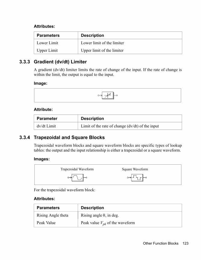
Attributes:
3.3.3 Gradient (dv/dt) LimiterA gradient (dv/dt) limiter limits the rate of change of the input. If the rate of change iswithin the limit, the output is equal to the input.
Image:
Attribute:
3.3.4 Trapezoidal and Square BlocksTrapezoidal waveform blocks and square waveform blocks are specific types of lookuptables: the output and the input relationship is either a trapezoidal or a square waveform.
Images:
For the trapezoidal waveform block:
Attributes:
Parameters Description
Lower Limit Lower limit of the limiter
Upper Limit Upper limit of the limiter
Parameter Description
dv/dt Limit Limit of the rate of change (dv/dt) of the input
Parameters Description
Rising Angle theta Rising angle θ, in deg.
Peak Value Peak value Vpk of the waveform
Trapezoidal Waveform Square Waveform
Other Function Blocks 123

12
For the square waveform block:
Attribute:
The waveforms of these two blocks are shown below. Note that the input vin is in deg.,and can be in the range of -360o to 360o. Both waveforms are half-wave and quarter-wave symmetrical.
3.3.5 Sampling/Hold BlockA sampling/hold block samples the input when the control signal changes from low tohigh (from 0 to 1), and holds this value until the next point is sampled.
Image:
The difference between this block and the zero-order hold block (ZOH) in DigitalControl Module is that this block is treated as a continuous element and samplingmoments can be controlled externally; whereas the zero-order hold block is a discreteelement and the sampling moments are fixed and of equal distance.
For a discrete system, the zero-order hold block should be used.
Example:In this example, a sinusoidal input is sampled. The control signal is a square wavevoltage source with an amplitude of 1.
Parameter Description
Pulse Width (deg.) Pulse width θ in half cycle, in deg.
θ
vo
Vpk
-Vpk
180o
360o
vin θ
vo
1
-1180
o360
o
vin
Trapezoidal Waveform Square Waveform
00
Input
Control
4 Control Circuit Components

3.3.6 Round-Off BlockThe image of a round-off block is shown below:
Image:
Attributes:
Let the input of the round-off block be Vin. The input is first scaled based on thefollowing expression:
If the truncation flag is 1, the output will be equal to Vin,new truncated, and then dividedby 10N. Otherwise, the output will be equal to Vin,new rounded off to the nearest integer,and then divided by 10N.
Examples:If Vin = 34.5678; N = 0, truncation flag = 0, then we have the output Vout = 35.
Similarly, if Vin = 34.5678; N = 0, truncation flag = 1, the output Vout = 34.
Parameters Description
No. of Digits No. of digits N after the decimal point
Truncation Flag Truncation flag (1: truncation; 0: round-off)
vinvo
vctrl
Vin new, Vin 10N⋅=
Other Function Blocks 125

12
If Vin = 34.5678; N = 1, truncation flag = 1, the output Vout = 34.5.
If Vin = 34.5678; N = -1, truncation flag = 1, the output Vout = 30.
3.3.7 Time Delay BlockA time delay block delays the input waveform by a specified amount of time interval. It,for example. can be used to model the propagation delay of a logic element.
Image:
Attribute:
Note that the difference between this block and the unit delay block (UDELAY) inDigital Control Module is that this block is a continuous element and the delay time canbe arbitrarily set; whereas the unit delay block is a discrete element and the delay time isequal to the sampling period.
For a discrete system, the unit delay block should be used.
Example:In this circuit, the first time delay block has a delay time of 1 ms, and the second blockhas a delay time of 4 ms. This example illustrates that the input of the time delay blockcan be either an analog or a digital signal.
Parameter Description
Time Delay Time delay, in sec.
vin1 vo1
vin2
vin2vo2
vo2
1 ms
4 ms
6 Control Circuit Components

3.3.8 MultiplexerThe output of a multiplexer is equal to a selected input depending on the control signal.Three multiplexers are provided: multiplexers with 2 inputs; 4 inputs; and 8 inputs.
Images:
In the images, d0..d7 are the data inputs; and s0..s2 are the control signals. The truthtables of the multiplexers are as follows.
Note that the data input could be either an analog or digital signal.
Example:The following circuit selects the maximum value out of two inputs. When Va is greaterthan Vb, the comparator output will be 1, and Vo = Va. Otherwise Vo = Vb.
2-Input MUX 4-Input MUX 8-Input MUXs0 Y s1 s0 Y s2 s1 s0 Y0 d0 0 0 d0 0 0 0 d01 d1 0 1 d1 0 0 1 d1
1 0 d2 0 1 0 d21 1 d3 0 1 1 d3
1 0 0 d41 0 1 d51 1 0 d61 1 1 d7
2-input 4-input 8-input
d0
d1
s0
s1s0 s2s1 s0
d0d1
d2d3
d0
d7
Y YY
Other Function Blocks 127

12
3.3.9 THD BlockThe total harmonic distortion (THD) of an ac waveform that contains both thefundamental and harmonic components is defined as:
where V1 is the fundamental component (rms), Vh is the harmonic rms value, and Vrms isthe overall rms value of the waveform. The THD block is modelled as shown below.
Image:
A second-order band-pass filter is used to extract the fundamental component. Thecenter frequency and the passing band of the band-pass filter need to be specified.
THDVh
V1-----
Vrms2 V1
2–V1
---------------------------= =
THD Circuit Model of the THD Block
vin(t) THD
v1(t)
V1
VhVrmsTHD
v1(t)
vin(t)
8 Control Circuit Components

Attributes:
Example: In the single-phase thyristor circuit below, a THD block is used to measure the THD ofthe input current. The delay angle of the thyristor bridge is chosen as 30o. For the THDblock, the fundamental frequency is set at 60 Hz and the passing band of the filter is setat 20 Hz. The simulation results are shown on the right.
One of the THD block output is the input current fundamental component is1. Bycomparing the phase difference between the input voltage vs and the current is1, one cancalculate the input displacement power factor. This, together with the THD value, canbe used to calculate the input power factor.
3.4 Logic Components
3.4.1 Logic GatesBasic logic gates are AND, OR, XORGATE (exclusive-OR), NOT, NAND, and NORgates.
Parameters Description
Fundamental Frequency Fundamental frequency of the input, in Hz
Passing Band Passing band of the band-pass filter, in Hz
vs
isis1
alpha=30 deg.
THD
Logic Components 129

13
Images:
3.4.2 Set-Reset Flip-FlopThere are two types of set-reset flip-flops. One is edge-triggered and the other is level-triggered.
Image:
Attribute:
An edge-triggered flip-flop only changes the states at the rising edge of the set/resetinput. The truth table of an edge-triggered flip-flop is:
A level-triggered flip-flop, on the other hand, changes the states based on the inputlevel. The truth table of a level-triggered set-reset flip-flop is:
Parameter Description
Trigger Flag Trigger flag (0: edge-triggered; 1: level-triggered)
S R Q Qn0 0 no change0 ↑ 0 1↑ 0 1 0↑ ↑ not used
NOR
AND OR NOT
NAND3-input AND 3-input OR
XOR
0 Control Circuit Components

3.4.3 J-K Flip-FlopA J-K flip-flop is positive edge-triggered.
Image:
The truth table is:
3.4.4 D Flip-FlopA D flip-flop is positive edge-triggered.
Image:
S R Q Qn0 0 no change0 1 0 11 0 1 01 1 not used
J K D Q Qn0 0 ↑ no change0 1 ↑ 0 11 0 ↑ 1 01 1 ↑ Toggle
Logic Components 131

13
The truth table is:
3.4.5 Monostable MultivibratorIn a monostable multivibrator, the positive (or negative) edge of the input signal triggersthe monostable. A pulse, with the specified pulse width, will be generated at the output.
The output pulse width can be either fixed or adjusted through another input variable.The latter type of monostables is referred to as controlled monostables. Its on-time pulsewidth, in second, is determined by the control input.
Images:
Attribute:
The input node at the bottom of the controlled monostable block is for the pulse widthinput.
3.4.6 Pulse Width CounterA pulse width counter measures the width of a pulse. The rising edge of the inputactivates the counter. At the falling edge of the input, the output gives the width of thepulse (in sec.). During the interval of two falling pulse edges, the pulse width counteroutput remains unchanged.
D Clock Q Qn0 ↑ 0 11 ↑ 1 0
Parameter Description
Pulse Width On-time pulse width, in sec.
Controlled MonostableMonostable
2 Control Circuit Components

Image:
3.4.7 Up/Down CounterAn up/down counter increments or decrements by 1 at each rising edge of the clock.
Image:
Attribute:
When the Up/Down input is 0, the counter decrements, and when the Up/Down input is1, the counter increments.
The Reset input resets the counter to 0 when it is high (1).
The Preset Enable input sets the counter to the preset value when it is high.
The truth table of the counter is:
x: Do not care
Parameter Description
No. of Bits Number of bits N
Up/Down Preset Enable Reset Clock Actionx 0 0 x No count1 0 0 ↑ Count up0 0 0 ↑ Count downx 1 0 x Presetx x 1 x Reset
Preset ValuePreset Enable
Up/DownReset
Clock Output
Logic Components 133

13
3.4.8 A/D and D/A ConvertersA/D and D/A converters perform analog-to-digital and digital-to-analog conversion.Both 8-bit and 10-bit converters are provided.
Images:
Let N be the number of bits. The output of the A/D converter is calculated as:
For example, if Vref = 5 V, Vin = 3.2 V, N = 8 bits, then
Vo = 256/5*3.2 = 163.84 = 10100011 (binary)
The output of the D/A converter is calculated as:
For example, if Vref = 5 V, Vin = 10100011 (binary) = 163, N = 8 bits, then
Vo = 163/256*5 = 3.1836
ADC (8-bit) ADC (10-bit) DAC (8-bit) DAC (10-bit)
Vin Vo
Vref Vref
Clock
Vo Vin
Vo2N
Vref--------- Vin⋅=
VoVref
2N--------- Vin⋅=
4 Control Circuit Components

3.5 Digital Control ModuleThe Digital Control Module is an add-on module to the basic PSIM program. It providesdiscrete elements, such as zero-order hold, z-domain transfer function blocks, digitalfilters, etc., for digital control system simulation.
In contrary to a s-domain circuit which is continuous, a z-domain circuit is discrete, andthe calculation is only performed at the discrete sampling points. There is no calculationbetween two sampling points.
3.5.1 Zero-Order HoldA zero-order hold samples the input at the point of sampling. The output remainsunchanged between two sampling points.
Image:
Attribute:
Like all other discrete elements, the zero-order hold has a free-running timer whichdetermines the moment of sampling. The sampling moment is synchronized with theorigin of the simulation time. For example, if the zero-order hold has a samplingfrequency of 1000 Hz, the input will be sampled at 0, 1 msec., 2 msec., 3 msec., and soon.
Example: In the following circuit, the zero-order hold sampling frequency is 1000 Hz. The inputand output waveforms are shown on the left.
Parameter Description
Sampling Frequency Sampling frequency of the zero-order hold, in Hz
Digital Control Module 135

13
Note that in above circuit, a continuous-domain integrator is also connected to the inputsine source. This makes it a mixed continuous-discrete circuit, and a simulation timestep selected for the continuous circuit will be used. With this time step, the familiarstaircase-like waveform can be observed at the zero-order hold output.
Without the integrator, the circuit becomes a discrete circuit. Since only the calculationat the discrete sampling points is needed, the simulation time step will be equal to thesampling period, and only the results at the sampling points are available. Thewaveforms, as shown below, appear continuous. In fact the waveforms are discrete, andthe connection between two sampling points makes it look like continuous.
3.5.2 z-Domain Transfer Function BlockA z-domain transfer function block is expressed in polynomial form as:
If a0 = 1, the expression Y(z) = H(z) * U(z) can be expressed in difference equation as:
H z( )b0 zN b1 zN 1–⋅ ... bN 1– z bN+⋅+ + +⋅
a0 zN a1 zN 1–⋅ ... aN 1– z aN+⋅+ + +⋅-------------------------------------------------------------------------------------------=
6 Control Circuit Components

Image:
Attributes:
Example:The following is a second-order transfer function:
Assuming a sampling frequency of 3 kHz, the specification will be:
Parameters Description
Order N Order N of the transfer function
Coeff. b0...bN Coefficients of the numerator (from b0 to bN)
Coeff. a0...aN Coefficients of the denominator (from a0 to aN)
Sampling Frequency Sampling frequency, in Hz
Order N 2
Coeff. b0...bN 0. 0. 400.e3
Coeff. a0...aN 1. 1200. 400.e3
Sampling Frequency 3000.
y n( ) b0 u n( ) b1 u n 1–( )⋅ ... bN u n N–( ) –⋅+ + +⋅=
a1 y n 1–( )⋅ a2 y n 2–( )⋅ ... aN y n N–( )⋅+ + +[ ]
H z( ) 400.e3
z2 1200 z 400.e3+⋅+----------------------------------------------------=
Digital Control Module 137

13
3.5.2.1 IntegratorThere are three types of integrators: regular integrator, external resettable integrator, andinternal resettable integrator.
Images:
Attribute:
The output of an external resettable integrator can be reset by an external control signal(at the bottom of the block). With the edge reset (reset flag = 0), the integrator output isreset to zero at the rising edge of the control signal. With the level reset (reset flag = 1),the integrator output is reset to zero as long as the control signal is high (1).
The output of an internal resettable integrator is reset to 0 whenever the output reacheseither the lower limit or the upper limit. The integrator works in the same way as theexternal resettable integrator with the edge reset, except that users do not need to set upthe external reset circuit in this case.
If we define u(t) as the input, y(t) as the output, T as the sampling period, and H(z) as thediscrete transfer function, the input-output relationship of an integrator can be expressed
Parameters Description
Algorithm Flag Flag for integration algorithm0: trapezoidal rule1: backward Euler2: forward Euler
Initial Output Value Initial output value
Reset Flag Reset flag (0: edge reset; 1: level reset) (for external resettable integrator only)
Lower Output Limit Lower limit of the output (for internal resettable integrator only)
Upper Output Limit Upper limit of the output (for internal resettable integrator only)
Sampling Frequency Sampling frequency, in Hz
Regular Integrator External Resettable Integrator Internal Resettable Integrator
8 Control Circuit Components

under different integration algorithms as follows.
With trapezoidal rule:
With backward Euler:
With forward Euler:
3.5.2.2 DifferentiatorThe transfer function of a discrete differentiator is:
where T is the sampling period. The input-output relationship can be expressed indifference equation as:
Image:
H z( ) T2--- z 1+
z 1–-----------⋅=
y n( ) y n 1–( ) T2--- u n( ) u n 1–( )+( )⋅+=
H z( ) T zz 1–-----------⋅=
y n( ) y n 1–( ) T u n( )⋅+=
H z( ) T 1z 1–-----------⋅=
y n( ) y n 1–( ) T u n 1–( )⋅+=
H z( ) 1T--- z 1–
z-----------⋅=
y n( ) 1T--- u n( ) u n 1–( )–( )⋅=
Digital Control Module 139

14
Attribute:
3.5.2.3 Digital FiltersTwo types of digital filters are provided: general digital filter and finite impulseresponse (FIR) filter. For both types, the filter coefficients can either be entered directlythrough the element property window, or be specified through a text file.
Images:
Attributes:For elements that read the coefficients directly:
For elements that read the coefficients from a text file:
The transfer function of the general digital filter is expressed in polynomial form as:
Parameter Description
Sampling Frequency Sampling frequency, in Hz
Parameters Description
Order N Order N of the transfer function
Coeff. b0...bN Coefficients of the numerator (from b0 to bN)
Coeff. a0...aN Coefficients of the denominator (from a0 to aN)
Sampling Frequency Sampling frequency, in Hz
Parameters Description
File for Coefficients Name of the file storing the filter coefficients
Sampling Frequency Sampling frequency, in Hz
FIR FilterGeneral Digital Filter
H z( )b0 b1 z 1–⋅ ... bN 1– z N 1–( )– bN z N–⋅+⋅+ + +
a0 a1 z 1–⋅ ... aN 1– z N 1–( )– aN z N–⋅+⋅+ + +--------------------------------------------------------------------------------------------------------=
0 Control Circuit Components

If a0 = 1, the output y and input u can be expressed in difference equation form as:
If the denominator coefficients a0..aN are not zero, this type of filter is called infiniteimpulse response (IIR) filter.
The transfer function of the FIR filter is expressed in polynomial form as:
If a0 = 1, the output y and input u can be expressed in difference equation form as:
The coefficient file for block FILTER_D1 and FILTER_FIR1 has the following format:
For Filter_FIR1:
For Filter_D1, the format can be either one of the following:
Nb0b1... ... ...bN
Nb0 b1 ... ... ...bN a0a1... ... ...aN
or Nb0, a0b1, a1... ... ...bN, aN
y n( ) b0 u n( ) b1 u n 1–( )⋅ ... bN u n N–( ) –⋅+ + +⋅=
a1 y n 1–( )⋅ a2 y n 2–( )⋅ ... aN y n N–( )⋅+ + +[ ]
H z( ) b0 b1 z 1–⋅ ... bN 1– z N 1–( )– bN z N–⋅+⋅+ + +=
y n( ) b0 u n( ) b1 u n 1–( )⋅ ... bN u n N–( )⋅+ + +⋅=
Digital Control Module 141

14
Example:To design a 2nd-order low-pass Butterworth digital filter with the cut-off frequency fc =1 kHz, assuming the sampling frequency fs = 10 kHz, using MATLAB, we have:
Nyquist frequency fn = fs / 2 = 5 kHz
Normalized cut-off frequency fc* = fc/fn = 1/5 = 0.2
[B,A] = butter (2, fc*)
which will give:
B = [0.0201 0.0402 0.0201 ] = [b0 b1 b2]
A = [ 1 -1.561 0.6414 ] = [a0 a1 a2]
The transfer function is:
The input-output difference equation is:
The parameter specification of the filter in PSIM will be:
If the coefficients are stored in a file, the file content will be:
20.02010.04020.02011.-1.5610.6414
Or the file can also have the content as follows:
Order N 2
Coeff. b0...bN 0.0201 0.0402 0.0201
Coeff. a0...aN 1. -1.561 0.6414
Sampling Frequency 10000.
H z( ) 0.0201 0.0402 z 1–⋅ 0.0201 z 2–⋅+ +1 1.561– z 1–⋅ 0.6414 z 2–⋅+
-------------------------------------------------------------------------------------=
y n( ) 0.0201 u n( ) 0.0402 u n 1–( )⋅ 1.561 y n 1–( )⋅ 0.6414– y n 2–( )⋅+ +⋅=
2 Control Circuit Components

20.0201, 10.0402, -1.5610.0201, 0.6414
3.5.3 Unit DelayA unit delay block provides one sampling period delay to the input.
Image:
Attribute:
The difference between a unit delay block and a time delay block (TDELAY) is that theunit delay block is a discrete element and it delays the sampled points by one samplingperiod, whereas TDELAY is a continuous element and it delays the whole waveform bythe delay time specified.
3.5.4 Quantization BlockA quantization block simulates the quantization error during an A/D conversion.
Image:
Attributes:
Parameter Description
Sampling Frequency Sampling frequency, in Hz
Parameters Description
No. of Bits Number of bits N
Vin_min Lower limit of the input value Vin,min
Vin_max Upper limit of the input value Vin,max
Digital Control Module 143

14
A quantization block performs two functions: scaling and quantization.
The input value Vin, sampled at the given sampling frequency, is first scaled based onthe following:
The number of bits determines the output resolution ΔV which is defined as:
The output Vo will be equal to the truncated value of Vox based on the resolution ΔV.
Example:If N = 4, Vin,min = 0, Vin,max = 10, Vo,min = -5, Vo,min = 5, and Vin = 3.2, then:
Vox = -5 + (3.2 - 0) * (5 - (05)) / (10 - 0) = -1.8
ΔV = (5 - (-5)) / (24 - 1) = 0.66667
The value -1.8 is between -2.33332 and -1.66665. Therefore, the lower value is selected,that is, Vo = -1.66665.
3.5.5 Circular BufferA circular buffer is a memory location that can store an array of data.
Image:
Vo_min Lower limit of the output value Vo,min
Vo_max Upper limit of the output value Vo,max
Sampling Frequency Sampling frequency, in Hz
Vox Vin min,Vin Vin min,–
Vin max, Vin min,–--------------------------------------- Vo max, Vo min,–( )+=
ΔVVo max, Vo min,–
2N 1–------------------------------------=
4 Control Circuit Components

Attributes:
A circular buffer stores data in a buffer. When the pointer reaches the end of the buffer,it will start again from the beginning.
The output of the circular buffer is a vector. To access to each memory location, use thememory read block MEMREAD.
Example:If a circular buffer has a buffer length of 4 and a sampling frequency of 10 Hz, we havethe buffer storage at different time as follows:
3.5.6 Convolution BlockA convolution block performs the convolution of two input vectors. The output is also avector.
Image:
Let the two input vectors be:
A = [ am am-1 am-2 ... a1]
Parameters Description
Buffer Length The length of the buffer
Sampling Frequency Sampling frequency, in Hz
Time InputValue at Memory Location
1 2 3 4
0 0.11 0.11 0 0 0
0.1 0.22 0.11 0.22 0 0
0.2 0.33 0.11 0.22 0.33 0
0.3 0.44 0.11 0.22 0.33 0.44
0.4 0.55 0.55 0.22 0.33 0.44
... ... ...
Digital Control Module 145

14
B = [ bn bn-1 bn-2 ... b1]
We have the convolution of A and B as:
= [cm+n-1 cm+n-2 ... c1]
where ci = Σ [ ak+1 * bj-k], k=0, ..., m+n-1; j=0, ..., m+n-1; i=1, ..., m+n-1
Example:If A = [1 2 3] and B = [4 5], we have m = 3; n = 2; and the convolution of A and B is:C = [4 13 22 15].
3.5.7 Memory Read BlockA memory read block is used to read the value of a memory location of a vector.
Image:
Attribute:
A memory read block allows one to access the memory location of elements such asconvolution block, vector array, and circular buffer. The index offset defines the offsetfrom the starting memory location.
Example:Let a vector be A = [2 4 6 8]. If index offset is 0, the memory read block output will be2. If the index offset is 2, the output will be 6.
3.5.8 Data ArrayThis is a one-dimensional array. The output is a vector. The data are either entereddirectly (the element is called Array in the PSIM library) or specified in a file (theelement is called Array (1) in the PSIM library).
Parameter Description
Memory Index Offset Offset from the starting memory location
C A B⊗=
6 Control Circuit Components

Image:
Attributes:
If the array is read from a file, the file will have the following format:
Na1... ... ...aN
where N is the length of the array, and a1..aN are the array values.
Example:To define an array A = [2 4 6 8], we will have: Array Length = 4; Values = 2 4 6 8. If thearray is to be read from a file, the file will be:
42.4.6.8.
Parameters Description
Array Length The length of the data array N (for the element Array only)
Values Values of the array (for the element Array only)
File for Coefficients Name of the file storing the array (for the element Array (1) only)
Digital Control Module 147

14
3.5.9 StackA stack is a first-in-last-out register.
Image:
Attribute:
The rising edge triggers the push or pop action. When a pop action is performed and thestack is empty, the output remains unchanged. When a push action is performed and thestack is already full, the data at the bottom of the stack will be pushed out and will belost.
3.5.10 Multi-Rate Sampling SystemA discrete system can have more than one sampling rate. The following system is usedto illustrate this.
The system below has 3 sections. The first section has a sampling rate of 10 Hz. Theoutput, Vo, fed back to the system and is sampled at 4 Hz in the second section. In thethird section, the output is displayed at a sampling rate of 2 Hz.
It should be noted that a zero-order hold must be used between two elements withdifferent sampling rates.
Parameter Description
Stack Depth The stack depth
Vin
pushpop
Vo
8 Control Circuit Components

Vo
Digital Control Module 149

15
3.6 SimCoupler ModuleThe SimCoupler Module is an add-on module to the basic PSIM software. It providesinterface between PSIM and Matlab/Simulink for co-simulation. With the SimCouplerModule, part of a system can be implemented and simulated in PSIM, and the rest of thesystem in Simulink. One can therefore make full use of PSIM’s capability in powersimulation and Matlab/Simulink’s capability in control simulation in a complementaryway.
The SimCoupler interface consists of two parts: the link nodes in PSIM, and theSimCoupler model block in Simulink. The images are shown below.
Images:
In PSIM, the SLINK_IN nodes receive values from Simulink, and the SLINK_OUTnodes send the values to Simulink. They are all control elements and can be used in thecontrol circuit only. In Simulink, the SimCoupler model block is connected to the rest ofthe system through input/output ports.
3.6.1 Set-up in PSIM and SimulinkThe use of the SimCoupler Module is easy and straightforward. As an example, thefollowing shows a permanent-magnet synchronous motor (PMSM) drive system withthe power stage implemented in PSIM, and the control in Simulink.
SimCoupler Model BlockSLINK_IN SLINK_OUT
In PSIM In SimuLink
0 Control Circuit Components

The following are the steps to set up SimCoupler for PSIM-Matlab/Simulink co-simulation for the example above.
Adding the SimCoupler Block to the Simulink Library:Run the program "SetSimPath.exe" to add the SimCoupler block to theSimulink library and set up the SimCoupler Module for co-simulation of PSIMand Matlab/Simulink. After the execution, the SimCoupler block will appear as"S-function SimCoupler" in the Simulink Library Browser.
Note that this step is necessary, otherwise Simulink will not be able to findPSIM. With this, it is also not necessary to manually add the PSIM folder to theMatlab path.
Also, this program needs to be run only once. It needs to be run again only ifthe PSIM folder or Matlab folder has changed.
Power
Control
in PSIM
in SimuLink
File: pmsm_simulink.mdl
File: pmsm_psim.sch
SimCoupler Module 151

15
In PSIM:- After the rest of the power circuit is created, connect three SLINK_OUT nodes
to the low-pass filters of Phase A, B, and C currents, and rename them as “Ia”,“Ib”, and “Ic”; and connect one SLINK_OUT node to the speed sensor outputand rename it as “Wrpm”.
- Connect three SLINK_IN nodes to the positive inputs of the comparators, andrename them as “Va”, “Vb”, and “Vc”.
- Go to the Simulate menu, and select Arrange SLINK Nodes. A dialog window will appear. Arrange the order of the SLINK_IN nodes and SLINK_OUT nodes to be the same as how the input/output ports would appear in the SimCoupler model block in Simulink (the order of the ports is from the top to the bottom). In this example, the order will be “Va”, “Vb”, and “Vc” for the SLINK_IN nodes, and “Ia”, “Ib”, “Ic”, and “Wrpm” for the SLINK_OUT nodes.
- Save the schematic file. In this example, we assume that the file is saved to “C:\PSIM\pmsm_psim.sch”.
In Simulink:- Start Matlab.
- Launch Simulink. Open an existing file or create a new file. After the rest of the system is created, go to the menu "S-function SimCoupler" in the Simulink Library Browser, select the SimCoupler block, and place it on the schematic.
- In the PMSM example file, double click on the SimCoupler block, and click onthe Browser button to locate and select the PSIM schematic file“C:\PSIM\pmsm_psim.sch”. Then click on Apply. The number of input andoutput ports of the SimCoupler model block will automatically match thosedefined in the PSIM netlist. In this case, there will be 3 input ports and 4 outputports.
- Go to the Simulation menu and select Simulation Parameters. Under SolverOptions, set the Type to “Fixed-step”. Set Fixed step size to be the same as orclose to PSIM’s time step. In this case, the time step is set to 0.1ms. Morediscussion on the selection of the solver option and the time step is given in thenext section.
- The setup is now complete. Go to Simulink and start the simulation.
The SimCoupler Module supports Matlab/Simulink Release 13 and 14.
Please also note that when the SimCoupler model block is used in a feedback system inSimulink, the SimCoupler model block may be part of an algebraic loop (please refer to
2 Control Circuit Components

Matlab Help for more information on algebraic loops). Some versions of Matlab/Simulink can not solve a system containing algebraic loops, and other can solve thesystem but with degraded performance. To break an algebraic loop, place a memoryblock at each output of the SimCoupler model block. The memory block introduces oneintegration time step delay.
3.6.2 Solver Type and Time Step Selection in SimulinkThere are certain restrictions on the selection of the solver type and the time step inSimulink when performing the co-simulation. To illustrate this, we use the followingone-quadrant chopper circuit with average current mode control as an example.
The circuit on the left is all implemented and simulated in PSIM. The circuit on the righthas the power stage implemented in PSIM, and the control implemented in Simulink. Inboth circuits, the PSIM simulation time step is 2 us.
There are different ways of setting up Simulink to perform co-simulation. Therecommend approach is to set the Solve Type to Fixed-step and define the Fixed stepsize to be the same or close to PSIM’s time step. The figure below shows this option.
Complete circuit in PSIM Power circuit in PSIM
Time step: 2us
SimCoupler Module 153

15
It is recommended that Simulink use the same time step as PSIM, although we havefound that, even if the Simulink time step is slightly larger than PSIM time step,satisfactory results are obtained. In this case, for example, the time step is set to 20 us,10 times larger than the PSIM time step.
If the Simulink Solver type is instead set to Variable-step, the simulation results willnot be correct. The figure below shows this option.
When the Simulink Solver type is set to Variable-step, in order to obtain correct results,a zero-order-hold must be placed at the input of the SimCoupler model block. Moreover,the zero-order-hold sample time must be the same or close to PSIM time step. Thefigure below shows the configuration.
Control in SimulinkTime step: 20 usSolver Type: Fixed-step
Control in Simulink Solver Type: Variable-step
4 Control Circuit Components

Therefore, Simulink must be set up to have the Solver Type as Fixed-step with the timestep the same or close to the PSIM time step, or if the Solver Type is Variable-step, azero-order-hold must be used with the sample time the same or close to PSIM time step
Control in Simulink Solver Type: Variable-stepZOH Sample Time: 2 us
SimCoupler Module 155

15
6 Control Circuit Components
4 Other Components
4.1 Parameter FileThe parameter file element .FILE defines the name of the file that stores the componentparameters and limit settings. For example, the resistance of a resistor can be specifiedas R1, and the value of R1 is defined in the parameter file.
Image:
The parameter file is a text file created by the user. The format is shown below:
<name> = <value>
<name> <value>
LIMIT <name> <lower limit> <upper limit>
% A comment line
The field <value> can be either a numerical number (e.g. “R1 = 12.3”) or amathematical expression (e.g. “R3 = R1 + R2/2.”). The name and the value can beseparated by either an equation sign (e.g. “R1 = 12.3”) or a space (e.g. “R1 12.3”). Textfrom the character “%” to the end of the line is treated as comments (e.g. “% R3 is theload resistance”).
For example, a parameter file may look like the following:
R1=12.3 [R1 is defined as 12.3]
R2 23.4Ohm [Equation sign can be replaced by space]
% R3 is the load resistance [This line is comments]
R3=R1+R2/2. [Math expression is allowed]
L1=3m [power-of-ten suffix is allowed. L1=0.003]
C1=100uF
Parameter File 157

15
LIMIT R3 5. 25. [R3 is limited between 5. and 25.]
4.2 SourcesSeveral types of independent voltage/current sources are available in PSIM. Thenotation of a current source direction is: the current flows out of the higher-potentialnode, through the external circuit, and back into the lower-potential node of the source.
Note that current sources can be used in the power circuit only.
4.2.1 TimeThe Time element is a special case of the piecewise linear voltage source. It is treated asa grounded voltage source, and the value is equal to the simulation time, in sec.
Image:
4.2.2 DC SourceA dc source has a constant amplitude. The reference of the grounded dc voltage sourcesis the ground.
Images:
Attribute:
Parameter Description
Amplitude Amplitude of the source
DC CurrentGrounded DC Grounded DC (1)DC (battery)
8 Other Components
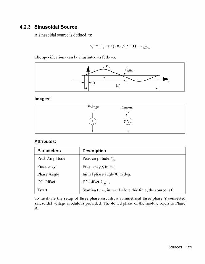
4.2.3 Sinusoidal SourceA sinusoidal source is defined as:
The specifications can be illustrated as follows.
Images:
Attributes:
To facilitate the setup of three-phase circuits, a symmetrical three-phase Y-connectedsinusoidal voltage module is provided. The dotted phase of the module refers to PhaseA.
Parameters Description
Peak Amplitude Peak amplitude Vm
Frequency Frequency f, in Hz
Phase Angle Initial phase angle θ, in deg.
DC Offset DC offset Voffset
Tstart Starting time, in sec. Before this time, the source is 0.
vo Vm 2π f t θ+⋅ ⋅( )sin⋅ Voffset+=
VoffsetVm
1/fθ t
Voltage Current
Sources 159

16
Image:
Attributes:
4.2.4 Square-Wave SourceA square-wave voltage source or current source is defined by peak-to-peak amplitude,frequency, duty-cycle, and DC offset. The duty cycle is defined as the ratio between thehigh-potential interval versus the period.
Images:
Parameters Description
V (line-line-rms) Line-to-line rms voltage amplitude
Frequency Frequency f, in Hz
Init. Angle (phase A) Initial angle for Phase A
3-phase Voltage
a
b
c
Voltage Current
0 Other Components

Attributes:
The specifications of a square wave source are illustrated as follows.
When the phase delay θ is positive, the waveform is shifted to the right along the timeaxis.
4.2.5 Triangular SourceA triangular-wave voltage source (VTRI) or current source (ITRI) is defined by peak-to-peak amplitude, frequency, duty-cycle, and DC offset. The duty cycle is defined asthe ratio between the rising-slope interval versus the period.
Images:
Parameters Description
Vpeak-peak Peak-to-peak amplitude Vpp
Frequency Frequency, in Hz
Duty Cycle Duty cycle D of the high-potential interval
DC Offset DC offset Voffset
Phase Delay Phase delay θ of the waveform, in deg.
Voffset
Vpp
tT (T=1/f)
D*T
0
θ
Voltage Current
Sources 161

16
Attributes:
The specifications of a triangular wave source are illustrated as:
When the phase delay θ is positive, the waveform is shifted to the right along the timeaxis.
4.2.6 Step SourcesA step voltage/current source changes from one level to another at a given time. Twotypes of step sources are provided: one that changes from 0 to a certain level (refer to asStep in the library), and the other that changes from one level to another level (referredto as Step (1) in the library).
Images:
Parameters Description
Vpeak-peak Peak-to-peak amplitude Vpp
Frequency Frequency, in Hz
Duty Cycle Duty cycle D of the rising slope interval
DC Offset DC offset Voffset
Phase Delay Phase delay θ of the waveform, in deg.
Voffset
Vpp
tT
(T=1/f)
D*T
0
θ
Voltage Current
2 Other Components

Attributes:For the Step type source:
For the Step (1) type source:
The specifications of the voltage step sources are illustrated as follows:
4.2.7 Piecewise Linear SourceThe waveform of a piecewise linear source consists of piecewise linear segments. It isdefined by the number of points, the values and the corresponding time (in sec.). Thevalues and times can be entered either separately, or in pair.
Images:
Parameters Description
Vstep Value Vstep after the step change
Tstep Time Tstep at which the step change occurs
Parameters Description
Vstep1 Value Vstep1 before the step change
Vstep2 Value Vstep2 after the step change
Tstep Time Tstep at which the step change occurs
T_transition Transition time Ttransition from Vstep1 to Vstep2
t0 Tstep
Vstep
t0 Tstep
Vstep2
TtransitionVstep1
Step (1) TypeStep Type
Voltage Current
Sources 163

16
Attributes:For the sources that define the values and times separately:
For the sources that define the values and times in pair:
The time and value pair must be enclosed by left and right brackets. The time and valuecan be separated by either a comma, such as (1.2m,5.5), or a space, such as (1.2m 5.5),or both, such as (1.2m, 5.5).
Example: The following is a non-periodic piecewise linear source. It has 3 segments which can bedefined by four points (marked in the figure).
The specification for the piecewise linear voltage source will be:
Parameters Description
Frequency Frequency of the waveform, in Hz
No. of Points n No. of points
Values V1...Vn Values at each point
Time T1...Tn Time at each point, in sec.
Parameters Description
Frequency Frequency of the waveform, in Hz
Times, Values (t1,v1) ... Time and value at each point
Frequency 0.
No. of Points n 4
Values V1...Vn 1. 1. 3. 3.
Times T1...Tn 0. 0.1 0.2 0.3
0 0.1 0.2 0.3
1
23
Time (sec.)
4 Other Components

The specification for the piecewise linear (1) voltage source will be:
4.2.8 Random SourceThe amplitude of a random voltage source (VRAND) or current source (IRAND) isdetermined randomly at each simulation time step. A random source is defined as:
where Vm is the peak-to-peak amplitude of the source, n is a random number in therange of 0 to 1, and Voffset is the dc offset.
Images:
Attributes:
4.2.9 Math Function SourceA math function source allows one to define the source in a mathematical expression.
Image:
Frequency 0.
Times, Values (t1,v1)... (0., 1) (0.1, 1) (0.2, 3) (0.3, 3)
Parameters Description
Peak-Peak Amplitude Peak-to-peak amplitude of the source
DC Offset DC offset
vo Vm n Voffset+⋅=
Voltage Current
Sources 165

16
Attributes:
In the expression, “T” or “t” represents time. For example, to implement a sinusoidalsource, the expression will be: sin(2*3.14159*60*t+2.09).
4.2.10 Voltage/Current-Controlled SourcesThe following types of controlled sources are available:
- Voltage controlled voltage source - Current controlled voltage source - Voltage controlled current source - Current controlled current source - Variable-gain voltage controlled voltage source - Variable-gain voltage controlled current source
The controlling current of a current controlled source must come from a RLC branch.Also, for a controlled current source, the controlling voltage or current can not be anindependent source.
Note that controlled sources can be used in the power circuit only.
Images:
Parameters Description
Expression The mathematical expression of the source
Tstart Start time of the source
Voltage-controlled Current-controlled
Voltage-controlled Current-controlled
Variable-gain
Variable-gain
vin1 vin2
vin1 vin2
Current-controlled (1)
Current-controlled (1)
voltage-controlled
voltage-controlled
6 Other Components

Attribute:
For voltage-controlled sources, the controlling voltage is from the positive node (+) tothe negative node (-).
For current-controlled sources (with an arrow pointing from one node to another), thecontrol nodes are connected across a RLC branch, and the direction of the controllingcurrent is indicated by the arrow.
For current-controlled sources (with a wire connecting the two nodes), the controllingcurrent flows from one control node to another, as indicated by the arrow. A 10-uOhmresistor is used to sense the controlling current.
The output of a controlled source, except variable-gain controlled sources, is equal tothe gain multiplied by the controlling voltage or current. For the variable-gaincontrolled sources, the output is equal to the following:
Input 1 is on the side with the multiplication sign, and Input 2 is on the side with theletter k.
The difference between a variable-gain controlled source and a nonlinear source withmultiplication is that, for the nonlinear source with multiplication, values of both vin1and vin2 at the current time step are used to calculate the output and are updated in eachiteration. But for the variable-gain controlled source, it is assumed that the change ofvin2 is small from one time step to the next, and the value of vin2 at the previous timestep is used at the current time step. This assumption is valid as long as vin2 changes at amuch slower rate as compared to vin1 and the time step is small as compared to thechange of vin2. Variable-gain controlled sources can be used in circuits which mayotherwise have convergence problem with nonlinear sources with multiplication.
Example:The circuits below illustrates the use of current controlled voltage sources.
In the circuit on the left, the voltage source is controlled by the inductor current is. Witha gain of 1, the waveform of the voltage vis is equal to that of is. In this way, a currentquantity can be converted to a voltage quantity.
Parameter Description
Gain Gain of the source
vo k vin2⋅( ) vin1⋅=
io k vin2⋅( ) vin1⋅=
Sources 167

16
The circuit on the right is equivalent to that on the left, except that a different currentcontrolled source is used instead.
4.2.11 Nonlinear Voltage-Controlled SourcesThe output of a nonlinear voltage-controlled source is either the multiplication, division,or square-root of the inputs. They are defined as:
Nonlinear (multiplication): Output or
Nonlinear (division): Output or
Nonlinear (square-root): Output or
Nonlinear (power): Output
In the nonlinear power source, the term sign(vin) is 1 if vin is positive, and it is -1 if vin isnegative.
Note that these nonlinear sources can be used in the power circuit only.
Images:
Vis
is
Vis
is
vo k vin1 vin2⋅ ⋅= io k vin1 vin2⋅ ⋅=
vo kvin1
vin2--------⋅= io k
vin1
vin2--------⋅=
vo k vin1⋅= io k vin1⋅=
vo sign vin( ) k k1 vin⋅( )k2⋅ ⋅=
Multiplication Division Square-root
vin1 vin2
vin2vin1
Power
8 Other Components

Attributes:For all the sources except the nonlinear power source:
For the nonlinear power source:
For the nonlinear (division) source, Input 1 is on the side of the division sign.
4.3 Voltage/Current SensorsVoltage/current sensors measure the voltages/currents of the power circuit and sendthem to the control circuit. The current sensor has an internal resistance of 1 μΩ.
Images:
Attribute:
4.4 Probes and MetersProbes and meters are used to measure voltages, currents, power, or other quantities. Avoltage probe (VP) measures a node voltage with respect to ground. A two-terminalvoltage probe (VP2) measures the voltage between two nodes. A current probe (IP)measures the current through the probe. Note that all the probes and meters, except thenode-to-ground probe VP, are allowed in the power circuit only.
Parameter Description
Gain Gain k of the source
Parameters Description
Gain Gain k of the source
Coefficient k1 Coefficient k1
Coefficient k2 Coefficient k2
Parameter Description
Gain Gain of the sensor
ISENVSEN
Voltage/Current Sensors 169

17
While probes measure a voltage or current quantity in its true form, meters can be usedto measure the dc or ac voltage/current, or the real power and reactive power. Thesemeters function in the same way as the actual meters.
A small resistor of 1 μΩ is used in the current probe internally to measure the current.
Images:
Attributes:
A low-pass filter is used in the dc meter and wattmeter models to filter out high-frequency components, whereas a high-pass filter is used in the ac meter and VAR meter
Parameters Description
Operating Frequency Operating frequency or fundamental frequency of the ac meter, in Hz
Cut-off Frequency Cut-off frequency of the low-pass/high-pass filter, in Hz
VA Display Flag Display flag for apparent power (0: no display; 1: display)
PF Display Flag Display flag for power factor (0: no display; 1: display)
DPF Display Flag Display flag for displacement power factor (0: no display; 1: display)
AC VoltmeterDC Voltmeter AC AmmeterDC Ammeter
Wattmeter VAR Meter 3-phase Wattmeter 3-phase VAR Meter
Voltage Probe Current Probe
VA-Power Factor Meter 3-phase VA-Power Factor Meter
0 Other Components

models to filter out the dc component. The cut-off frequency determines the transientresponse of the filter.
Except the voltage and current probes, the readings of all the meters are meaningfulonly when the readings reach the steady state.
For the single-phase VA-Power Factor meter, the apparent power (S), total power factor(PF), and the displacement power factor (DPF) are defined as follows.
Assume both the voltage and current contains harmonics, i.e.
where ω1 is the fundamental frequency and all others are harmonic frequencies. Wehave the rms values of the voltage and current as:
The apparent power is defined as:
The real power (or average power) is defined as:
where T is the fundamental period. The total power factor PF and the displacementpower factor DPF are then defined as follow:
For the three-phase circuit, the definitions are similar. Note that the meter VA_PF3 is forthe 3-phase 3-wire circuit, and the summation of the three phase voltages or currentsmust be equal to zero, that is:
v t( ) 2V1 ω1t φ1+( )sin 2V2 ω2t φ2+( )sin ...+ +=
i t( ) 2I1 ω1t θ1+( )sin 2I2 ω2t θ2+( )sin ...+ +=
Vrms V12 V2
2 ...+ +=
Irms I12 I2
2 ...+ +=
S Vrms Irms⋅=
P 1T--- v t( ) i t( )⋅( ) td
0
T
∫=
PF PS---=
DPF φ1 θ1–( )cos=
Probes and Meters 171

17
4.5 Voltage/Current ScopesWhile voltage/current probes and meters save the simulation results for post waveformprocessing, voltage/current scopes allow users to view simulation waveforms at runtimein the middle of the simulation.
Three scopes are provided: 1-channel voltage scope, 2-channel voltage scope, andcurrent scope.
Below are the images of the voltage and current scopes and their expanded view.
The 1-channel voltage scope and the current scope have the same interface.
The scope is designed to operate in a similar way as the actual oscilloscope in the lab. Ithas 3 main sections: Timebase section, Channel section, and Trigger section.
In the Timebase section, the scale of time (x axis) is defined.
In the Channel section, the scale of the Y axis, as well as the offset and the color of the
va vb vc+ + 0=
ia ib ic+ + 0=
2-channel voltage scope 1-channel voltage scope Current scope
2 Other Components

waveform, are defined.
In the Trigger section, the trigger conditions are defined. The trigger can be set to eitherON or OFF. When the trigger is off, the waveform is free-running, and the display of thewaveform in the scope may vary from one frame to another. If the trigger is on, thewaveform display will only start when the trigger conditions are met. This will lead to asteady waveform display.
There are three trigger modes: rising-edge triggering, falling-edge triggering, and one-shot triggering (if the once checkbox is checked, the one-shot triggering is selected).The one-shot triggering will trigger only once, and it is useful, for example, in situationswhere a transient needs to be captured.
The trigger level sets the level at which the triggering occurs. For example, if Channel Ais selected with the rising-edge triggering and the trigger level of 0V, whenever theChannel A input crosses over 0 from negative to positive, triggering will occur and thewaveform display will start from that instant.
Note that voltage scopes have connecting terminals which can be connected to eitherpower circuit nodes or control circuit nodes. The scopes will display the node-to-groundvoltages at these nodes.
The current scope, on the other hand, has no connecting terminals. It is associated withany element that has the parameter of the current flag, and it is enabled by right clickingon top of the element, and selecting the branch current under the Current Scopes, asshown below. After the branch current is selected, a check mark will appear in front ofthe branch current name.
Voltage/Current Scopes 173

17
If the element has multiple current flags, under the Current Scopes menu, there will bemultiply branch currents, one corresponding to each current flag.
For example, for a 3-phase resistor R1, under the Current Scopes menu, there will bethree branch currents:
I(R1) AI(R1) BI(R1) C
The letter "A", "B", and "C" refer to Channel A, B, and C, respectively. For example, if"I(R1) A", "I(R1) B", and "I(R1) C) are all selected, in the current scope, one can go tothe Channel pull-down menu in the Channel section, and select one of the channels fordisplay. If Channel A is selected, the scope will show the Phase A branch current I(R1).
4.6 Switch ControllersA switch controller has the same function as a switch gate/base drive circuit in an actualcircuit. It receives the input from the control circuit, and controls switches in the powercircuit. One switch controller can control multiple switches simultaneously.
4.6.1 On-Off Switch ControllerOn-off switch controllers are used as the interface between control gating signals andpower switches. The input, which is a logic signal (either 0 or 1) from the controlcircuit, is passed to the power circuit as the gating signal.
Image:
Example:The circuit below implements the step change of a load. In the circuit, the on-off switchcontroller is used to control the bi-directional switch. The step voltage source, which isconnected to the controller input, changes from 0 to 1 at the time of 12 ms. The closureof the switch results in the short-circuit of the resistor across the switch and the increaseof the current.
4 Other Components

4.6.2 Alpha ControllerAn alpha controller is used for delay angle control of thyristor switches or bridges.There are three input for the controller: the alpha value, the synchronization signal, andthe gating enable/disable signal. The transition of the synchronization signal from lowto high (from 0 to 1) provides the synchronization and this corresponds to the momentwhen the delay angle alpha equals zero. A gating with a delay of alpha degrees isgenerated and sent to the thyristors. The alpha value is updated instantaneously.
Image:
Attributes:
The input for the delay angle alpha is in deg.
Parameters Description
Frequency Operating frequency of the controlled switch/switch module, in Hz
Pulse Width On-time pulse width of the switch gating, in deg.
On-offController
Enable/Disable
alphaSync.Signal
Switch Controllers 175

17
Example: The figure below shows a thyristor circuit using delay angle control. In the circuit, thezero-crossing of vs, which corresponds to the moment that the thyristor would startconducting naturally, is used to provide the synchronization. The delay angle is set at30o. The gating signal is delayed from the rising edge of the synchronization signal by30o.
4.6.3 PWM Lookup Table ControllerThere are four input signals in a PWM lookup table controller: the modulation index,the delay angle, the synchronization signal, and the gating enable/disable signal. Thegating pattern is selected based on the modulation index. The synchronization signalprovides the synchronization to the gating pattern. The gating pattern is updated whenthe synchronization signal changes from low to high. The delay angle defines therelative angle between the gating pattern and the synchronization signal. For example, ifthe delay angle is 10 deg., the gating pattern will be leading the synchronization signalby 10 deg.
Image:
vs
vsync
iRL1
Enable/Disable
Mod. Index
Sync.DelaySignalAngle
6 Other Components

Attributes:
A lookup table, which is stored in a file, contains the gating patterns. It has thefollowing format:
n, m1, m2, ..., mnk1G1,1, G1,2, ..., G1,k1... ... ...knGn,1, Gn,2, ..., Gn,kn
where n is the number of gating patterns; mi is the modulation index correspondent toPattern i; and ki is the number of switching points in Pattern i. The modulation indexarray m1 to mn should be monotonically increasing. The output will select the ith patternif the input is smaller than or equal to mi. If the input exceeds mn, the last pattern will beselected.
The following table shows an example of a PWM pattern file with five modulationindex levels and 14 switching points.
5, 0.901, 0.910253, 0.920214, 1.199442, 1.21147.736627 72.10303 80.79825 99.20176 107.8970 172.2634 180. 187.7366 252.1030 260.7982 279.2018 287.8970 352.2634 360.147.821098 72.27710 80.72750 99.27251 107.7229 172.1789 180.187.8211 252.2771 260.7275 279.2725 287.7229 352.1789 360.147.902047 72.44823 80.66083 99.33917 107.5518 172.0979 180.
Parameters Description
Frequency Switching frequency, in Hz
Update Angle Update angle, in deg., based on which the gatings are internally updated. If the angle is 360o, the gatings are updated at every cycle. If it is 60o, the gatings are updated at every 60o.
File Name Name of the file storing the PWM gating pattern
Switch Controllers 177

17
187.9021 252.4482 260.6608 279.3392 287.5518 352.0980 360.1410.186691 87.24225 88.75861 91.24139 92.75775 169.8133 180.190.1867 267.2422 268.7586 271.2414 272.7578 349.8133 360.1410.189426 87.47009 88.97936 91.02065 92.52991 169.8106 180.190.1894 267.4701 268.9793 271.0207 272.5299 349.8106 360.
In this example, if the modulation index input is 0.8, the controller will select the firstgating pattern. If the modulation index is 0.915, the controller will select the thirdpattern.
Example: This example shows a three-phase voltage source inverter (file: “vsi3pwm.sch”). ThePWM for the converter uses the selected harmonic elimination. The gating patterns aredescribed above and are pre-stored in File “vsi3pwm.tbl”. The gating pattern is selectedbased on the modulation index. The waveforms of the line-to-line voltage and the three-phase load currents are shown below.
8 Other Components

4.7 Function Blocks
4.7.1 Control-Power Interface BlockA control-power interface block passes a control circuit value to the power circuit. It isused as a buffer between the control and power circuit. The output of the interface blockis treated as a constant voltage source when the power circuit is solved. With this block,some of the functions that can only be generated in the control circuit can be passed tothe power circuit.
Image:
Example: A Constant-Power Load ModelIn a constant-power dc load, the voltage V, current I, and power P have the relationshipas P=V*I. Given the voltage and the power, the current can be calculated as I=P/V. Thiscan be implemented using the circuit as shown below.
The load voltage is measured through a voltage sensor and is fed to a divider. The outputof the divider gives the current value I. Since the voltage could be zero or a low value atthe initial stage, a limiter is used to limit the current amplitude. This value is convertedinto the load current quantity through a voltage-controlled current source.
Example: The following circuit illustrates how a control circuit signal can be passed to the powercircuit. As seen from the power circuit, the CTOP block behaviors as a groundedvoltage source.
P
IV
k=1
LOAD
Function Blocks 179

18
4.7.2 ABC-DQO Transformation BlockThe ABC-DQO function blocks perform the abc-dqo transformation. They convertthree voltage quantities from one coordinate to another. These blocks can be used ineither the power circuit or the control circuit.
Images:
It should be noted that, in the power circuit, currents must first be converted into voltagequantities (using current-controlled voltage sources) before they can be transformed.Also, if an input terminal is not used (such as in the DQO-to-ABC transformation blockwhere only Phase D and Q are not used, and Phase O is not used), it must be connectedto ground.
The transformation equations from abc to dqo are:
The transformation equations from dqo to abc are:
Control Circuit Power Circuit
ABC to DQO DQO to ABC
θ θ
vd
vq
vo
23---
θcos θ 2π3
------–⎝ ⎠⎛ ⎞cos θ 2π
3------+⎝ ⎠
⎛ ⎞cos
θsin θ 2π3
------–⎝ ⎠⎛ ⎞sin θ 2π
3------+⎝ ⎠
⎛ ⎞sin
12--- 1
2--- 1
2---
va
vb
vc
⋅ ⋅=
0 Other Components

Example:In this example, three symmetrical ac waveforms are transformed into dqo quantities.The angle θ is defined as θ = ωt where ω = 2π*60. Since the angle θ changes linearlywith time, a piecewise linear voltage which has a ramp waveform is used to represent θ.The simulation waveforms show the three-phase ac (top), the angle θ (middle), and thedqo output. In this example, the “q” component is constant, and both the “d” and the “o”components are zero.
4.7.3 Math Function BlocksThe output of a math function block is expressed as the mathematical function of theinputs. With this block, one can implement complex and nonlinear relationship easily.Blocks with 1, 2, 3, 5, and 10 inputs are provided.
Images:
va
vb
vc
θcos θsin 1
θ 2π3
------–⎝ ⎠⎛ ⎞cos θ 2π
3------–⎝ ⎠
⎛ ⎞sin 1
θ 2π3
------+⎝ ⎠⎛ ⎞cos θ 2π
3------+⎝ ⎠
⎛ ⎞sin 1
vd
vq
vo
⋅=
Function Blocks 181

18
Attributes:
The derivative df/dxi can be set to zero.
The variables that are allowed in the expression are: T or t for time, and xi (i from 1 to n)which represents the ith input. For example, for the 3-input math function block, theallowed variables are: T, t, x1, x2, and x3. For the 1-input math function block, thevariable x, which refers to the only input, is also allowed.
4.7.4 Lookup TablesThere are three types of lookup tables: one-dimensional lookup table, 2-dimensionallookup table with integer inputs, and 2-dimensional lookup table with floating-pointinputs.
All three types of lookup tables can be used in both power circuit and control circuit.
Images:
Parameters Description
Expression f(x1,x2,...,xn)
Expression of the output versus inputs where n is the number of inputs
Expression df/dxi Expression of the derivative of the function f versus the ith input
1-input 2-input 3-input 5-input 10-input
1-dimensional 2-dimensional
Index i
Index j
2 Other Components

Attribute:
For the 2-dimensional lookup table block, the node at the left is for the row index input,and the node at the top is for the column index input.
The one-dimensional lookup table has one input and one output. Two data arrays,corresponding to the input and the output, are stored in the lookup table in a file. Theformat of the table is as follows.
Vin(1), Vo(1)Vin(2), Vo(2)...Vin(n), Vo(n)
The input array Vin must be monotonically increasing. Between two points, linearinterpolation is used to obtain the output. When the value of the input is less than Vin(1)or greater than Vin(n), the output will be clamped to Vo(1) or Vo(n).
The 2-dimensional lookup table with integer input has two inputs. The output data isstored in a 2-dimensional matrix. The two input correspond to the row and columnindices of the matrix. For example, if the row index is 3 and the column index is 4, theoutput will be A(3,4) where A is the data matrix. The data for the lookup table are storedin a file and have the following format:
m, nA(1,1), A(1,2), ..., A(1,n)A(2,1), A(2,2), ..., A(2,n)... ... ...A(m,1), A(m,2), ..., A(m,n)
where m and n are the number of rows and columns, respectively. Since the row or thecolumn index must be an integer, the input value is automatically converted to aninteger. If either the row or the column index is out of the range (for example, the rowindex is less than 1 or greater than m), the output will be zero.
The 2-dimensional lookup table with floating-point inputs is similar to the 2-dimensional lookup table with integer inputs. The difference is that in this case, inputsare floating-point values, and interpolation is used to calculate the output.
The data for the lookup table are stored in a file and have the following format:
Parameter Description
File Name Name of the file storing the lookup table
Function Blocks 183

18
m, nVr,1 Vr,2 ... Vr,mVc,1 Vc,2 ... Vc,nA(1,1), A(1,2), ..., A(1,n)A(2,1), A(2,2), ..., A(2,n)... ... ...A(m,1), A(m,2), ..., A(m,n)
where m is the number of rows and n is the number of columns; Vr is the row vector andVc is the column vector; and A(i,j) is the output value at Row i and Column j. Note thatVectors Vr and Vc must be monotonically increasing.
If the input falls between two points, interpolation is used to calculate the value. If theinput is less than the minimum or greater than the maximum value, the input will be setto be the same as the minimum or maximum value.
Examples: The following shows a one-dimensional lookup table:
1., 10.2., 30.3., 20.4., 60.5., 50.
If the input is 0.99, the output will be 10. If the input is 1.5, the output will be
=20.
The following shows a 2-dimensional lookup table with integer inputs:
3, 41., -2., 4., 1.2., 3., 5., 8.3., 8., -2., 9.
If the row index is 2 and the column index is 4, the output will be 8. If the row index is5, regardless of the column index, the output will be 0.
The following shows a 2-dimensional lookup table with floating-point inputs:
3, 41.1 2.2 3.3
10 1.5 1–( ) 30 10–( )⋅2 1–
------------------------------------------------+
4 Other Components

1.2 2.3 3.4 4.51., -2., 4., 1.2., 3., 5., 8.3., 8., -2., 9.
If the row input is 2 and the column input is 3, the following table shows the four pointsthat enclose the input point, and the output value of 3.826 through interpolation:
4.7.5 C Script BlockThe C script block allows users to enter C code directly without compiling the code,unlike in the case of external DLL blocks where users need to compile the code into aDLL using a compiler. The code of the C script block will be interpreted and executed atruntime by a built-in C interpreter in PSIM.
This block makes it very easy to support custom C codes, and to define and modify thefunctionality of the block.
The interface of the C script block dialog window is shown below.
In the Number of Input/Output Ports section, the number of input and output ports of theports is defined. After the number of ports is changed, the image of the block in theschematic will change accordingly.
In the Function Type section, there are four choices:
Variable/Function Definitions: For includes statements and global variabledefinition.
OpenSimUser Fcn: The function that is called only once at thebeginning of the simulation for initialization.
RunSimUser Fcn: The function that is called at each simulation step.CloseSimUser Fcn: The function that is called only once at the end of
the simulation for termination.
When one of the choices is selected, the area underneath shows the corresponding code.The complete code consists the combined code of all the four parts.
Column
2.3 3 3.4
1.1 -2 4
Row 2 2.091 3.826 4.818
2.2 3 5
Function Blocks 185

18
Click on the Check Code button to check if the code has any compiling errors. Click onthe Edit Image button to customize the image of the C script block.
The difference between the C script block and the external DLL block is that, eventhough the C script block is easier to use, it does have the disadvantage that the customcode in the C script block can not be debugged, while in the external DLL block it ispossible to set break points and trace/step through the code for debugging.
4.7.6 External DLL BlocksAn external DLL (dynamic link library) block allows users to write code in C/C++,compile it into DLL using Microsoft Visual C/C++, and link it with PSIM. These blockscan be used in either the power circuit or the control circuit.
A DLL block receives values from PSIM as inputs, performs the calculation, and sendsthe results back to PSIM. PSIM calls the DLL routine at each simulation time step.However, when the inputs of the DLL block are connected to one of these discreteelements (zero-order hold, unit delay, discrete integrators and differentiators, z-domain
Area forcustom code
Functionselection
Input/outputports
6 Other Components

transfer function blocks, and digital filters), the DLL block is called only at the discretesampling times.
Two types of DLL blocks are provided: Simple DLL Block and General DLL Block.The simple DLL block has a fixed number of inputs and outputs, and the DLL file nameis the only parameter that needs to be defined. On the other hand, the general DLL blockallows users to define arbitrary number of inputs/outputs and additional parameters.Users can also customize the DLL block image.
In general, the simple DLL block is easier to program and easier to use.
The images and parameters of the simple DLL blocks are shown below.
Images:
Attribute:
The node with a dot is for the first input (in[0]). The sequence of the input/output nodesis from the top to the bottom.
The images and parameters of the simple DLL blocks are shown below.
Image (for a block with 2 inputs and 3 outputs):
Parameter Description
File Name Name of the DLL file
1-input 3-input 6-input
1
3
1
3
22
input output
1 1
6 6
1 1
3
22
input output
Function Blocks 187

18
Attribute:
The node with a dot is for the first input (in[0]). The sequence of the input/output nodesis from the top to the bottom.
By default, users define the number of inputs and outputs. But the number of inputs andoutputs, the node names, as well as the number of parameters and the parameter namescan all be defined inside the DLL routine. For more details on defining andprogramming for the general DLL block, please refer to the help file "Help GeneralDLL Block.pdf" and related examples.
The name of the DLL file can be arbitrary. The DLL file can be placed in one of thethree places, in the order of precedence: in the PSIM directory, in the same directory asthe schematic file that uses the DLL file, or in the directory as defined in the Options ->Set Path function in PSIM.
Sample DLL files are provided in PSIM, and users can use these files as the templates to
Parameter Description
DLL File Name of the DLL file
Input Data File Name of the input data file that the DLL routine reads (optional)
Number of Input Nodes
Number of input nodes (optional)
Number of Output Nodes
Number of output nodes (optional)
IN Nodes List of input nodes (optional)
OUT Nodes List of output nodes (optional)
Parameter 1 Parameter to be passed from PSIM into the DLL routine (optional)
Parameter 2 Parameter to be passed from PSIM into the DLL routine (optional)
Edit Image (button) Click this button to edit and customize the image of the DLL block.
Display File (button) Click this button to display the content of the Input Data File (optional).
Read File (button) If the Input Data File is modified, click this button to reload the data file (optional).
8 Other Components

write their own. Procedures on how to compile the DLL routine and link with PSIM areprovided in these files and in the on-line help.
Example:The following shows a power factor correction circuit with the inductor current and theload voltage feedback. The input voltage is used to generate the current reference. Thecontrol scheme is implemented in a digital environment, with a sampling rate of 30 kHz.The control scheme is implemented in an external C code and is interfaced to the powercircuit through a simple DLL block.
The input of the DLL block are the sampled input voltage, inductor current, and outputvoltage. One of the DLL block outputs is the modulation wave Vm, which is comparedwith the carrier wave to generate the PWM gating signal for the switch. The otheroutput is the inductor current reference for monitoring purpose.
Part of the source code, which is in the file “pfc_vi_dll.c”, is shown below. Both theinner current loop and the outer voltage loop use a PI controller. Trapezoidal rule is usedto discretize the controllers. Discretization using Backward Euler is also implementedbut the codes are commented out.
Function Blocks 189

19
// This sample program implement the control of the circuit "pfc-vi-dll.sch" in a C routine. // Input: in[0]=Vin; in[1]=iL; in[2]=Vo// Output: Vm=out[0]; iref=out[1]// You may change the variable names (say from "t" to "Time").// But DO NOT change the function name, number of variables, variable type, and sequence.// Variables:// t: Time, passed from PSIM by value// delt: Time step, passed from PSIM by value// in: input array, passed from PSIM by reference// out: output array, sent back to PSIM (Note: the values of out[*] can be modified in PSIM)// The maximum length of the input and output array "in" and "out" is 20.// Warning: Global variables above the function simuser (t,delt,in,out) are not allowed!!!#include <math.h>__declspec(dllexport) void simuser (t, delt, in, out)// Note that all the variables must be defined as "double"double t, delt;double *in, *out;{
// Place your code here............begindouble Voref=10.5, Va, iref, iL, Vo, Vm, errv, erri, Ts=33.33e-6;static double yv=0., yi=0., uv=0., ui=0.;// InputVa=fabs(in[0]);iL=in[1];Vo=in[2];// Outer Looperrv=Voref-Vo;// Trapezoidal Ruleyv=yv+(33.33*errv+uv)*Ts/2.;iref=(errv+yv)*Va;// Inner Looperri=iref-iL;// Trapezoidal Ruleyi=yi+(4761.9*erri+ui)*Ts/2.;Vm=yi+0.4*erri;// Store old valuesuv=33.33*errv;ui=4761.9*erri;// Outputout[0]=Vm;out[1]=iref;// Place your code here............end
}
0 Other Components

4.7.7 Embedded Software BlockThe Embedded Software Block is a special type of the external DLL blocks. It isintended for modeling embedded software devices such as microcontrollers and DSP.
Attribute:
The Embedded Software Block has similar functionality as the general external DLLblock. However, unlike the general DLL block whose connection nodes are predefinedas either inputs or outputs, the Embedded Software Block allows the node types to beprogrammed as needed.
Also, additional information, such as the exact instant at which the state of a variablechanges, can be calculated and passed to and from PSIM.
The Embedded Software Block is a control circuit element, and can be used in thecontrol circuit only.
For more information on how to use the Embedded Software Block, please refer to thedocument "Help Embedded Software Block.pdf".
Parameter Description
DLL File Name of the DLL file that defines the functionality and the interface of the block
Number of Nodes Total number of input and output nodes
Function Blocks 191

19
2 Other Components
5 Analysis Specification
5.1 Transient AnalysisThe transient analysis is set up by selecting Simulation Control in the Simulate menuin PSIM, and defining the parameters as follows.
With the SAVE and LOAD functions, the circuit voltages, currents and other quantitiescan be saved at the end of a simulation session, and loaded back as the initial conditionsfor the next simulation session. This provides the flexibility of running a longsimulation in several shorter stages with different time steps and parameters.Components values and parameters of the circuit can be changed from one simulationsession to the other. The circuit topology, however, must remain the same.
Time Step Simulation time step, in sec.
Total Time Total simulation time, in sec.
Free Run checkbox
When the Free Run checkbox is not checked, the simulation will run up to the Total Time and then stop. But when it is checked, the simulation will run in the free-run mode and it will keep on running until manually stopped.In the free-run mode, voltage/current scopes can be used to monitor and display voltages and currents in the middle of the simulation.
Print Time Time from which simulation results are saved to the output file. No output is saved before this time.
Print Step Print step. If the print step is set to 1, every data point will be saved to the output file. If it is 10, for example, only one out of 10 data points will be saved. This helps to reduce the output file size.
Load Flag Flag for the LOAD function. If the flag is 1, the previous simulation values will be loaded from a file (with the “.ssf” extension) as the initial conditions.
Save Flag Flag for the SAVE function. If the flag is 1, values at the end of the current simulation will be saved to a file with the “.ssf” extension.
Transient Analysis 193

19
In PSIM, the simulation time step is fixed throughout the simulation. In order to ensureaccurate simulation results, the time step must be chosen properly. The factors that limitthe time step in a circuit include the switching period, widths of pulses or waveforms,and intervals of transients. It is recommended that the time step should be at least onemagnitude smaller than the smallest of the above.
In PSIM, an interpolation technique is implemented which will calculate the exactswitching instants. With this technique, the error due to the misalignment of switchinginstants and discrete simulation points is significantly reduced. It is possible to simulatewith a large time step while still maintaining accurate results.
The allowable maximum time step is automatically calculated in PSIM. It is comparedwith the time step set by the user, and the smaller value of the two will be used in thesimulation. If the selected time step is different from the one set by the user, it will besaved to the file “message.txt”.
5.2 AC AnalysisThe frequency response of a circuit or a control loop can be obtained with the acanalysis. A key feature of the ac analysis in PSIM is that, a circuit can be in its originalswitchmode form, and no average model is required. Nevertheless, with the averagemodel, the time it takes to perform the ac analysis will be shorter.
The following are the steps to set up the ac analysis:
- Identify a sinusoidal voltage source as the excitation source for the ac sweep.
- Place ac sweep probes at the desired output location. To measure the loopresponse of a closed control loop, use the node-to-node probe.
- Place the .ACSWEEP element on the schematic, and define the parameters ofthe ac sweep.
- Run the simulation.
Below are the images of the ac sweep probes and the .ACSWEEP sweep element.
Images:
.ACSWEEPAC Sweep Probe AC Sweep Probe (loop)
4 Analysis Specification

Attributes:
The principle of the ac analysis is that a small ac excitation signal is injected into thesystem as the perturbation, and the signal at the same frequency is extracted at theoutput. To obtain accurate ac analysis results, the excitation source amplitude must beset properly. The amplitude must be small enough so that the perturbation stays in thelinear region. On the other hand, the excitation source amplitude must be large enoughso that the output signal is not affected by numerical errors.
In general, a physical system has low attenuation in the low frequency range and highattenuation in the high frequency range. A good selection of the excitation sourceamplitude would be to have a relatively small amplitude at the low frequency, and arelatively large amplitude at the high frequency.
Sometimes, after ac analysis is complete, a warning message is displayed as follows:Warning: The program did not reach the steady state after 60 cycles.See File “message.txt” for more details.
This message occurs when the software fails to detect the steady state at the ac sweepoutput after 60 cycles. To address this problem, one may increase damping in the circuit(by including parasitic resistances, for example), or adjust the excitation sourceamplitude, or reduce simulation time step. The file “message.txt” gives the informationon the frequency at which this occurs and the relative error. The relative error willindicate how far the data point is from reaching the steady state.
Parameters Description
Start Frequency Start frequency of the ac sweep, in Hz
End Frequency End frequency of the ac sweep, in Hz
No. of Points Number of data points
Flag for Points Flag to define how the data points is generated.Flag = 0: Points are distributed linearly in LOG10 scaleFlag = 1: Points are distributed linearly in linear scale
Source Name Name of the excitation source
Start Amplitude Excitation source amplitude at the start frequency
End Amplitude Excitation source amplitude at the end frequency
Freq. for extra Points Frequencies of additional data points. If the frequency-domain characteristics change rapidly at a certain frequency range, one can add extra points in this region to obtain better data resolution.
AC Analysis 195

19
Example: Impedance of Shunt FiltersThe circuit below consists of two shunt filters tuned at the 5th and 7th harmonics (thefundamental frequency is 60 Hz). By injecting the excitation source as the current andmeasuring the voltage, we obtain the impedance characteristics of the filters. The acanalysis waveform on the right clearly shows two troughs at 300 Hz and 420 Hz.
Example: Open-Loop Response of a Buck ConverterThe circuit on the left is an one-quadrant buck converter. An excitation source isinjected to the modulation signal, and the output voltage is measured. The result of theac analysis, on the right, shows the open-loop response of the output voltage versus themodulation signal.
6 Analysis Specification

Example: Loop Transfer Function of a Closed-Loop CircuitThe ac analysis can be used to find out the loop response of a closed-loop system. Thecircuit below shows a buck converter with average current mode control. By injectingthe excitation signal into the current feedback path, and using the node-to-node acsweep probe, we can obtain the loop transfer function directly. With the loop transferfunction, one can determine the bandwidth of the control loop and the phase margin.
Please note that the ac sweep probe should be connected such that the dotted side isconnected to the node after the excitation source injection.
Example: Loop Transfer Function of a Switchmode Power SupplyThe loop transfer function of a switchmode power supply controlled by a PWM IC canalso be determined in a similar way. The figure below shows a buck convertercontrolled by TI UC3842. The excitation source can be inserted in the feedback path,before the op. amp. output.
AC Analysis 197

19
5.3 Parameter SweepParameter sweep can be performed for the following parameters:
- Resistance, inductance, and capacitance of RLC branches
- Gain of proportional blocks
- Time constant of integrators
- Gain and time constant of proportional-integral controllers
- Gain, cut-off frequency, and damping ratio of 2nd-order low-pass and high-pass filters
- Gain, center frequency, and passing and stopping band of 2nd-order band-pass and band-stop filters
The image and parameters of the parameter sweep element are shown below.
8 Analysis Specification

Image:
Attributes:
For example, let the resistance of a resistor be “Ro”. To sweep the resistance from 2Ohm to 10 Ohm, with a step of 2 Ohm, the specification will be:
Parameters Description
Start Value Starting value of the parameter
End Value End value of the parameter
Increment Step Increment step
Parameter to be Swept Parameter to be swept
Start Value 2
End Value 10
Increment Step 2
Parameter to be Swept Ro
Parameter Sweep 199

20
0 Analysis Specification
6 Circuit Schematic Design
PSIM’s schematic program provides interactive and user-friendly interface for circuitschematic entry and editing. The following figure shows a boost power factor correctioncircuit in the PSIM environment.
In PSIM, all the elements are stored under the Elements menu. The elements aredivided into four groups: Power (for power circuit element), Control (for controlelements), Other (for switch controllers, sensors, probes, interface elements, andelements that are common to both power and control), and Sources (for voltage andcurrent sources).
Parameter Sweep 201

20
6.1 Creating a CircuitThe following functions are provided for circuit creation.
Get There are two ways to get an element from the element library.One is to use the pull-down menu. Go to the Elements menu, andgo into the submenu and highlight the element to be selected.
Another is to use the Library Browser, as shown below.
The Library Browser provides a convenient way of navigatingthrough the library. To display the Library Browser, go to View ->Library Browser.
Also, the most recent elements are listed in the pull-down button
on the toolbar.
Place Once an element is selected from the menu, the image of theelement will appear on the screen and move with the mouse. Clickthe left button of the mouse to place the element.
Rotate Before the element is placed, right click to rotate the element.After an element is selected, select Rotate to rotate the element.
2 Circuit Schematic Design

Wire To connect a wire between two nodes, select Wire. The image of apen will appear on the screen. To draw a wire, keep the left buttonof the mouse pressed and drag the mouse. A wire always startsfrom and end at a grid intersection.
For easy inspection, a floating node is displayed as a circle, and ajunction node is displayed as a solid dot.
Label If two or more nodes are connected to the same label, they areconnected. It is equivalent as though they were connected by wire.Using labels will reduce the cross-wiring and improve theschematic layout.
The text of a label can be moved. To select the text, left click onthe label, then press the Tab key.
Assign To assign the parameters of an element, double click on theelement. A dialog box will appear. Specify the values and hit the<Return> key or click on OK.
6.2 Editing a CircuitDouble left click or single right click on top of an element will bring up the propertydialog window. Also, to move the whole schematic, right click and drag the mouse.
The following functions are provided in the Edit menu for circuit editing:
Select To select an element, click on the element. A rectangle will appeararound the element.
To select a block of a circuit, keep the left button of a mousepressed and drag the mouse until the rectangle covers the selectedarea.
Copy To copy an element or a block of the circuit, select the element orthe region, and choose Copy. Then choose Paste place theelement or circuit.
Delete To delete an element, a block of a circuit, or a wire, select theitem, and choose Cut, or hit the <Delete> key. Note that if Cut isused, the last deleted item can be pasted back. This is equivalentto un-do.
Move To move an element or a circuit block, select the element/circuitblock and drag the mouse while keeping the left button pressed.
Text To place text on the screen, choose Text. Enter the text in the
Editing a Circuit 203

20
dialog box, and click the left button of the mouse to place it.
Disable To disable an element or part of a circuit. When the element or thecircuit is disabled, it will be grayed out and will be treated as non-existent as far as the simulation is concerned. This function isuseful if an element or circuit needs to be excluded but not deletedfrom the circuit.
Enable To enable a previously disabled element or circuit.
Escape Quit from any of the above editing modes by choosing Escape.
Copy to Clipboard To copy the schematic image to the clipboard which can then bepasted back in another software. One can choose either the Coloroption or the Black & White option. The Black & White optionwill result in a smaller image file size.
Drawing To draw images on the schematic for display purposes. Thefollowing images are provided: line, ellipse, rectangle, and half-circle.
Add/Remove To add or remove the current scope for elements that have current Current Scope flags. After this is selected, a scope image will appear with the
mouse. Then click on top of an element with the current flag, andselect the branch current name. Select the branch current again toremove the current scope.
Show/Hide To show or hide the parameters of elements that can be changed Runtime Variables at runtime in the middle of the simulation. After this is selected,
the text of the parameter will appear. Click on the text, and a small
dialog window will appear. Enter the new
value directly in the data field, and click Apply. Or alternatively,click on the up/down arrow keys on the keyboard to increase/decrease the value.
In addition, the following functions are provided in the View menu:
Zoom Select Zoom In to zoom in the circuit, or Zoom In Selected tozoom in to a selected region. Choose Zoom Out to zoom out, orFit to Page to zoom out to fit the entire circuit to the screen.
Element List To generate the parts list of the circuit.
Element Count To count the number of elements. Voltage/current probes andmeters are not included in the element count.
4 Circuit Schematic Design

Custom Toolbars To create customized toolbars.
Custom Keyboard To customize keyboard. Functions can be assigned to thekeyboard for easier circuit editing.
The procedures for create customized toolbars and to customize keyboards aredescribed below.
Customizing Toolbars:
To create a toolbar called "new" and add the AND gate to the toolbar, for example, dothe following:
- Choose View -> Custom Toolbars. The Custom Toolbars dialog window willappear. Choose New Toolbar, and the following window will appear.
- Specify the Toolbar Name as "new".
- Draw the AND gate icon in the icon editing area. Or if the icon is alreadyavailable in the predefined icon images, select the icon and copy it to the iconediting area.
- Under the Edit Command section, with the option Elements selected,highlight "AND Gate". Then click on the Add Button. The icon will appear inthe toolbar icon area. Click on OK to close the window, and go back to the
Iconediting area
Predefinedicon images
Toolbaricon area
Editing a Circuit 205

20
Custom Toolbars window.
- Check "new" in the Custom Toolbars dialog window, and the new toolbar willappear. Uncheck the box will hide the toolbar.
Customizing Keyboard:
To define the key "r" for getting a resistor from the library, for example, do thefollowing:
- Choose View -> Custom Keyboard. The Custom Toolbars dialog window willappear. Choose New Toolbar, and the following window will appear.
- In the section Add Shortcut Key, select the option Elements. Then find andhighlight the element "Resistor".
- Move the cursor into the input field of Press new shortcut key, and press thekey "r" on the keyboard. Then click on Assign.
- The key "r" will be assigned to the resistor, and the definition will appear in theCurrent Shortcut Key list.
6.3 Saving a FileAfter a schematic is created, it can be saved to a binary file by choosing the Save orSave As function in the File menu.
By choosing File -> Save with Password, one can protect a file with a password. Whena file is password protected, it can still be used in the simulation, but one needs to enterthe correct password in order to see the schematic. The password protection is used in
6 Circuit Schematic Design

situations where the person who created the file needs to share it with someone else, butdoes not wish to reveal the details of the schematic.
The function Save in Package File in the File menu allows users to save all the filesthat are associated with a simulation to one single file. This is especially useful if themain circuit calls multiple subcircuits, and one needs to send the files to someone else.Rather than finding and collecting all the subcircuit files, one can just create the packagefile and send the single file out.
The function Save as Version 6.2 in the File menu saves a file in the Version 6.2 format.Note that if the file uses elements that are unique in Version 7.0, these elements will beomitted. Also, Version 6.2 file format is very close to Version 6.1 format, and a file inVersion 6.2 format can be opened by PSIM Version 6.1.
6.4 SubcircuitThe following functions are provided for subcircuit editing and manipulation.
New Subcircuit To create a new subcircuit
Load Subcircuit To load an existing subcircuit. The subcircuit will appear on thescreen as a block.
Edit Subcircuit To edit the size and file name of the subcircuit
Set Size To set the size of the subcircuit
Place Port To place the connection port between the main circuit and thesubcircuit
Display Port To display the connection port of the subcircuit
Edit Default To edit the default variable list of the subcircuit Variable List
Edit Image To edit the subcircuit image
Display Subcircuit To display the subcircuit nameName
Show Subcircuit To display the port names of the subcircuit in the main circuit Ports
Hide Subcircuit To hide the port names of the subcircuit in the main circuit Ports
Subcircuit List To list the file names of the main circuit and the subcircuits
One Page up To go back to the main circuit. The subcircuit is automatically
Subcircuit 207

20
saved.
Top Page To jump from a lower-level subcircuit to the top-level maincircuit. This is useful for circuits with multiple layers ofsubcircuits.
The one-quadrant chopper circuit below illustrates the use of the subcircuit.
6.4.1 Creating Subcircuit - In the Main CircuitThe following are the steps to create the subcircuit “chop_sub.sch” in the main circuit“chop.sch”.
- Open or create the main circuit “chop.sch”.
- If the file “chop_sub.sch” does not exist, go to the Subcircuit menu, and selectNew Subcircuit. If the file exists, select Load Subcircuit instead.
- A subcircuit block (rectangle) will appear on the screen. Place the subcircuit.
6.4.2 Creating Subcircuit - Inside the SubcircuitTo enter the subcircuit, double click on the subcircuit block.
- Create/edit the content of the subcircuit circuit exactly the same way as in themain circuit.
- To specify the subcircuit size, select Set Size in the Subcircuit menu. In thisexample, the size is set to 4x7 (width of 4 divisions and height of 7 divisions).Note that the size of the subcircuit should be chosen such that it gives theproper appearance and allows easy wire connection in the main circuit.
- Once the subcircuit is complete, define ports to connect the subcircuit nodeswith the corresponding nodes in the main circuit. Choosing Place Port in theSubcircuit menu, and a port image will appear. After the port is placed in the
File: chop_sub.sch
Inside the subcircuit:
File: chop.sch
Subcircuit
8 Circuit Schematic Design

circuit, a pop-up window (shown on the left below) will appear.
The diamonds on the four sides represent the connection nodes and thepositions of the subcircuit. They correspond to the connection nodes of thesubcircuit block on the right. There are no diamonds at the four corners sinceconnections to the corners are not permitted.
When a diamond is selected, it is colored red. By default, the left diamond atthe top is selected and marked with red color. Click on the desired diamond toselect and to specify the port name.
In this example, in the main circuit “chop.sch”, there are four linking nodes,two on the left side and two on the right side of the subcircuit block. Therelative position of the nodes are that the upper two nodes are 1 division belowthe top and the lower two nodes are 1 division above the bottom.
To specify the upper left linking node, click on the top diamond of the left side,and type “in+”. The text “in+” will be within that diamond box and a portlabelled with “in+” will appear on the screen. Connect the port to the upper leftnode. The same procedure is repeated for the linking nodes “in-”, “out+”, and“out-”.
- After the four nodes are placed, the node assignment and the subcircuit appearin PSIM as shown below.
Subcircuit port assignments
Subcircuit 209

21
The creation of the subcircuit is now complete. Save the subcircuit, and go back to themain circuit.
6.4.3 Connecting Subcircuit - In the Main CircuitOnce the subcircuit is created and connection ports are defined, complete the connectionto the subcircuit block in the main circuit.
- In the main circuit, the connection points on the borders of the subcircuit blockappear as hollow circles.
- Select the subcircuit block, and select Show Subcircuit Ports in the Subcircuitmenu to display the port names as defined inside the subcircuit.
- Connect the wires to the connection points accordingly.
6.4.4 Other Features of the SubcircuitThis section describes other features of the subcircuit through the example shownbelow.
0 Circuit Schematic Design

6.4.4.1 Passing Variables from the Main Circuit to SubcircuitIn this example, the main circuit “main.sch” uses a subcircuit “sub.sch”. In thesubcircuit, the inductance value is defined as “L” and the capacitance is defined as “C”.The default values of L and C can be set by selecting Subcircuit | Set Default VariableList. In this case, L is set to 5mH and C is set to 100uF.
When the subcircuit is loaded into the main circuit the first time, this default variable listwill appear in the tab “Subcircuit Variables” in Subcircuit | Edit Subcircuit from themain circuit “main.sch”. New variables can be added here and variable values can bechanged. In this case, L is changed to 2mH, and C is kept the same as the default value.
Note that the variables and the values are saved to the netlist file and used in simulation.The default variable list inside the subcircuit is not saved to the netlist and is not usedfor simulation.
This feature allows the parameters of a subcircuit to be defined at the main circuit level.
File: sub.sch
Inside the subcircuit:File: main.sch
Subcircuit 211

21
In the case where the same subcircuit is used several times in one main circuit, differentparameters can be assigned to the same variable. For example, if the subcircuit“sub.sch” is used two times in above example, in one subcircuit L can be defined as3mH, and in another subcircuit L can be defined as 1mH.
Note that this example also illustrates the feature that parameters can be defined as avariable (for example “Vin” for the input dc voltage source) or a mathematicalexpression (for example “R1+R2” for the load resistance). The variables “Vin”, “R1”,and “R2”, are defined in the parameter file “para-main.txt”. See Section 4.1 for moredetails.
6.4.4.2 Customizing the Subcircuit ImageThe following are the procedures to customize the subcircuit image of “sub.sch”:
- In the subcircuit, select Edit Image in the Subcircuit menu. A window willpop-up, as shown below.
In the window, the diamonds marked red are the connection nodes of thesubcircuit block, in exactly the same positions as appearing in the main circuit.
- Use the drawing tool to create/edit the image for the subcircuit block. If thedrawing tool is not already displayed, go to the View menu and check DrawingTools. Click on Zoom In and Zoom Out icons on the toolbar to adjust the sizeof the image working area.
After the image is created, the pop-out window will appear as follows.
2 Circuit Schematic Design

- Go back to the subcircuit window (“sub.sch” in this case), and save the subcircuit. The new subcircuit block image should appear in the main circuit.
6.4.4.3 Including Subcircuits in the PSIM Element ListIf you create a directory called “User Defined” under the PSIM directory, and placesubcircuits inside this directory. subcircuits will appear as items in the Elements menu,under Elements | User Defined, just like any other PSIM elements. You can also createsubdirectories under the directory User Defined, and place subcircuits inside thesubdirectories. For example, the Elements menu may look like this:
- Power
- Control
- Other
- Sources
- Symbols
- User Defined
- Subcircuit 1
- Project A
- Subcircuit 2
Subcircuit 213

21
- Subcircuit 3
- Project B
- Subcircuit 4
In this way, common-used custom-built subcircuits can be grouped together and easilymanaged and accessed.
6.5 Running the SimulationTo run the simulation, choose Run PSIM from the Simulate menu. This will start thePSIM simulation.
To view the simulation results, choose Run SIMVIEW from the Simulate menu.
To view the simulation results in the middle of the simulation, one can either go toSimulate -> Runtime Graphs to select the waveforms, or use the voltage/currentscopes (under Elements -> Other -> Probes) to view the waveforms.
The difference between the runtime graphs and the voltage/current scopes is that onlywaveforms that are saved for display in SIMVIEW (such as voltage probes, currentprobes, current flags, etc.) are available for the runtime graphs. In addition, a runtimegraph display the waveform in its entirety, from the beginning to the final study time.Because of this, the runtime graphs are disabled in the free-run mode as the final studytime is undetermined.
On the other hand, voltage/current scopes can be used in either the one-time simulationmode or in the free-run mode. Voltage scopes can be connected to any nodes, and willdisplay the node-to-ground voltage waveforms. On the other hand, current scopes areavailable to elements that have current flags (such as R-L-C branches and switches).
Moreover, in the free-run mode, the majority of the element parameters can be changedduring runtime in the middle of the simulation. This makes it possible to tune a circuitwhile inspecting key waveforms using voltage/current scopes, until desiredperformance is achieved.
Running Simulation in the Free-Run Mode:
To illustrate how to run a simulation in the free-run mode, a buck converter circuitshown below is used as an example. The circuit on the left was originally set up for theone-time simulation, with the total simulation time set to a specific value.
4 Circuit Schematic Design

To set up the simulation in the free-run mode:
- In Simulation Control, check the Free Run checkbox.
- Go to Elements -> Other -> Scopes, and select the 2-channel voltage scope.Connect the scope as shown above on the right.
- Double click on the scope, and the scope image will appear. Start thesimulation, and the waveforms will appear and will be updated continuously inthe scope. Change the scope settings as desired.
- Elements parameters can now be adjusted in the middle of the simulation. Toadjust the gain of the PI controller, for example, right click on top of the PIblock, and choose Runtime Variables -> Gain. The text of the gain "0.6" willbe displayed if it has not been displayed already.
- Click on the text "0.6", and a small dialog window will appear. The screenshould look as follows.
One-time simulation Simulation in the free-run mode
Running the Simulation 215

21
- Place the cursor inside the input field of the dialog window for the gain, andchange the gain either by pressing on the upper/down arrow keys on thekeyboard, or by entering a new value and then clicking on Apply. Watch howthe waveforms change as the gain is changed.
Other parameters, such as current reference, dc input voltage, inductance,capacitance, and load resistance, can be changed in the similar way.
- Branch currents can also be displayed in the free-run mode. To display theinductor current, for example, right click on top of the inductor, and a menuwill appear. Choose Current Scopes and the branch current name.
- An image of the current scope (similar to the voltage scope image, but withoutconnection terminals) will appear. Double click on the scope to expand andview the inductor waveform.
Below is how the window would look like with both the voltage scope and thecurrent scope.
Other branch currents, such as capacitor current, load current, diode current, orMOSFET switch current, can be displayed in the similar way.
Gain of the PI controller
6 Circuit Schematic Design

Running Simulation with the Command-Line Option:
Simulation can also be launched with the command line option by running the programPsimCmd.exe. For example, to simulate the circuit "chop.sch" which is stored in thefolder "c:\psim\examples", go to the PSIM folder, and run the following command:
PsimCmd -i "c:\psim\examples\chop.sch" -o "c:\psim\examples\chop.smv"
The format of the command line is as follows:
PsimCmd -i "[input file]" -o "[output file]" -v "VarName1=VarValue1" -v "VarName2=VarValue2" -t "TotalTime" -s "TimeStep" -g
Note that the quotes around the parameter values must be present. The command-lineparameters are:
-i: Input schematic file name-o: Output file name (in either .txt or .smv extension)-v: Variable name and value. This parameter can be used multiple
times. For example, to define the resistance R1 as 1.5 and the inductance L1 as 0.001, we have: -v "R1=1.5" -v "L1=0.001"
Voltage scope
Current scope
Running the Simulation 217

21
-t: Total time of the simulation-s: Time step of the simulation-g Run SIMVIEW after the simulation is complete
With the command-line option, one can run several circuits automatically in a batch run.
6.6 Managing the PSIM LibraryThe PSIM library consists of two parts: one is the image library (psimimage.lib) and theother is the netlist library (psim.lib). The netlist library can not be modified. But userscan modify the image library, or create their own image library.
To create or modify the image library, go to Edit -> Edit Library -> Edit LibraryFiles, and follow the instructions on the screen. Any image libraries in the PSIMdirectory will be automatically loaded into PSIM.
There are two ways to add a custom model to the PSIM library list. One is to have themodel in the form of a subcircuit, and then place the schematic file in a folder calleduser defined in the PSIM directory, or in one of the sub-folders of the user definedfolder. Any schematic files and sub-folders under the user defined folder will appear inthe PSIM library list.
Another way is to add the custom model directly to an image library. The advantage ofthis approach is that the custom element will have the same look-and-feel as thestandard PSIM elements, giving it a better interface. It is also possible to associate ahelp file to the custom model.
Below are the procedures to add the custom models to the PSIM library.
6.6.1 Adding a New Subcircuit Element into the LibraryThere are three main steps to add a new element, modeled in a subcircuit, into the PSIMlibrary:
- Create the subcircuit model of the new element.
- Add this element to the PSIM library.
- Create an on-line help file for this new element.
To illustrate this process, a LC-filter element is used as an example.
Creating the Subcircuit:
The first step is to create the subcircuit of the new element in the same way as if thesubcircuit is to be called by another circuit. For example, the subcircuit of the 2nd-orderLC filter, called "LC_filter.sch", and its image are shown below:
8 Circuit Schematic Design

In this case, the inductance and capacitance values will be defined through the interface,and need to appear in the property window of the new LC filter element. Therefore, theparameter value for the inductance needs to be defined as a variable, in this case, L, andthe value for the capacitance as C.
Then from Subcircuit -> Edit Default Variable List, add the variables L and C as thedefault variables. This step is necessary as the new element obtains the parameterinformation from the default variable list. The default variable list window shouldappears as follows.
Here Variable Label is the text that describes the parameter, Variable Name is thevariable that is used as the parameter value in the subcircuit, and Variable Value is the
Managing the PSIM Library 219

22
default value of the parameter. For example, for the inductance L, the Variable Label isInductance, the Variable Name is L, and the Variable Value is 1m.
Adding the New Element to the PSIM Library:
To add the subcircuit element into the PSIM library, follow these steps:
- Go to Edit -> Edit Library -> Edit Library Files, and choose the library forthe new element. Click on New Library to create a new image library, or selectan existing library and click on Edit Selected Library.
- In the Library Editor, click on the button New Subcircuit. Enter theinformation to the dialog window as shown below:
The explanation of each field is as follows:
Name: Name of the new element as it appears in the PSIM libraryDescription: Description of the new elementFile Path: The location of the subcircuit schematic file
"LC_filter.sch". The subcircuit file must be placed in the\lib sub-folder in the PSIM directory.
Hide (menu): Leave this box unchecked. If this box is checked, thiselement will not appear in the library.
Help File: On-line help file associated with this element.Help ID: The ID used in the help map file to link the designated
help page.
- Click on the buttons Save Image Library and Update Menu. The newelement will appear in the library and will be ready to use.
0 Circuit Schematic Design

Creating the On-Line Help File for the New Element:
An on-line help file can be created for this new element, so that when the Help button isclicked in the property dialog window, the corresponding help page will come up. Thefollowing is the procedure to create the help file using Microsoft Help Workshop.
- Prepare the help content in the .rtf file "LC_Filter.rtf" using Microsoft Word.Note that the footnote of the file should look as follows:
#LC_FILTER$LC_FILTERkLC_FILTER; LC filter
Here the # label is used to link the help page with the LC filter element inPSIM. The k label will appear in the Index in the Help file, and the $ label isnot used.
- Prepare the help map file "HelpMap.txt". It is a text file, and has the followingcontent:
LC_FILTER=1001
Here the text "LC_FILTER" must be the same as the # label in the"LC_Filter.rtf" file, and the number "1001" must be the same as the Help IDdefined for the LC filter element when it was created.
- In the Help Workshop project file "LC_Filter.hpj", have the following settings:
- Click on the Files button, and add the file "LC_Filter.rtf".- Click on the Options button, and in the Files tab, set Help File as
LC_Filter.hlp.- Click on the Map button, and then click on Include to include the map
file HelpMap.txt.
- Click on Save and Compile to create the help file "LC_Filter.hlp". Place thisfile in the PSIM directory.
6.6.2 Adding a New DLL Element into the LibrarySimilar to that of a subcircuit element, there are three main steps to add a new element,modeled in a DLL, into the PSIM library:
- Create the model in the DLL file.
- Add this element to the PSIM library.
- Create an on-line help file for this new element.
Managing the PSIM Library 221

22
To illustrate this process, an inductor is used as an example.
Creating the DLL:
The first step is to create the inductance model in DLL. Please refer to the relevantsection on how to create a custom DLL.
Here we assume that the DLL file, "inductor_model.dll", has already been created usingthe Power Modeling Block. It has one parameter called "Inductance", and twoconnecting nodes.
Adding the New Element to the PSIM Library:
To add the DLL element into the PSIM library, follow these steps:
- Go to Edit -> Edit Library -> Edit Library Files, and choose the library forthe new element. Click on New Library to create a new image library, or selectan existing library and click on Edit Selected Library.
- In the Library Editor, click on the button New DLL File. Enter the informationto the dialog window as shown below:
The explanation of each field is as follows:
Name: Name of the new inductor element as it appears in thePSIM library
Description: Description of the new inductor elementFile Path: The location of the DLL file "inductor_model.dll" that
models the new inductor element. The DLL file must beplaced in the lib sub-folder in the PSIM directory.
Input Nodes: Number of input terminals of the new element. For the
2 Circuit Schematic Design

Power Modeling Block, this value is the number of totalterminals and is read from the DLL file automatically.
Output Nodes:Number of output terminals of the new element. For thePower Modeling Block, this value is 0.
Hide (menu): Leave this box unchecked. If this box is checked, thiselement will not appear in the library.
Help File: On-line help file associated with this element.Help ID: The ID used in the help map file to link the designated
help page.
- In the next dialog window, set the new element size as: Width = 5, and Height= 2. Then create an image for this element, or accept the default image.
- Click on the buttons Save Image Library and Update Menu. The newelement will appear in the library and will be ready to use.
The information regarding the number of parameters and the parameter description forthe new inductor element is obtained from the DLL file automatically. In this case, thenew element will have one parameter as "Inductance".
The process of creating the on-line help file is the same as described in the previoussection.
6.7 Other Options
6.7.1 Generate and View the Netlist FileTo generate the netlist, choose Simulate -> Generate Netlist File. This will create thenetlist file with the “.cct” extension. The netlist file will be saved to the same directoryas the schematic file.
To view the netlist file, choose Simulate -> View Netlist File.
6.7.2 Set PathThe Set Path function in the Options menu allows users to define additional searchpaths when loading an external DLL file. For example, if a schematic file uses a DLLfile, and this DLL file is placed in a directory other than the schematic directory or thePSIM directory, this directory can be included in PSIM by using the Set Path function.
PSIM searches the DLL files in the following order:
- PSIM directory
- Schematic file directory
Other Options 223

22
- Directories as defined in the Set Path function.
The first time that the DLL file is encountered, it will be loaded.
For example, assume that the PSIM program files are in C:\PSIM, the schematic file isin C:\TEMP; and the directory as defined in the Set Path function is C:\TEMPDLL.The DLL file can be in one of the three places:
- C:\PSIM
- C:\TEMP
- C:\TEMPDLL
6.7.3 SettingsGrid display, rubber band feature, text fonts, simulation warning, and colors can be setin the Settings... in the Option menu.
Before a circuit is printed, its position on the paper can be viewed by selecting PrintPage Border in the Settings... option. If a circuit is split into two pages, it can be movedinto one single page. If the circuit is too big to fit in one page, one can zoom out andreduce the circuit size by clicking the Zoom Out button.
Print page legend, such as company name, circuit title, designer’s name, date, etc., canbe specified by choosing Print Page Setup in the File menu. It can be disabled in theSettings... option.
Also in the Settings... option, if Disable simulation warning messages is checked,warning messages generated during the simulation will be suppressed. Otherwise,warning messages will be shown before waveforms are displayed in SIMVIEW.
6.7.4 Printing the Circuit SchematicThe circuit schematic can be printed from a printer by choosing Print in the File menu.It is also possible to print the selected region of a circuit by choosing Print Selected.
The schematic can also be saved to the clipboard which can be imported into a wordprocessor (such as Microsoft Word). By default, the schematic image is saved inmonochrome in order to save memory space. One can save the image in color byselecting Edit/Copy to Clipboard/Color.
4 Circuit Schematic Design

7 Waveform Processing
SIMVIEW is PSIM’s waveform display and post-processing program. The followingshows simulation waveforms in the SIMVIEW environment.
SIMVIEW reads data in either ASCII text format or SIMVIEW binary format. Thefollowing shows a sample text data file:
Functions in each menu are explained in the following sections.
Time Isa Isc Isb Tem_IM 5.000000000E-006 0.000000000E+000 0.000000000E+000 0.000000000E+000 7.145888260E-048 1.000000000E-005 0.000000000E+000 0.000000000E+000 0.000000000E+000 1.082981714E-046 1.500000000E-005 0.000000000E+000 0.000000000E+000 0.000000000E+000 5.408644357E-046 2.000000000E-005 1.139566166E-001 -2.279132474E-001 1.139566166E-001 1.613605209E-017 2.500000000E-005 5.072914178E-001 -1.014582858E+000 5.072914178E-001 3.598226665E-015 ... ... ... ...
Other Options 225

22
7.1 File MenuThe File Menu has the following functions:
Open Load a data file in ASCII text format (with .txt extension) orSIMVIEW binary format (with .smv extension)
Merge Merge another data file with the existing data file for display
Re-Load Data Re-load data from the same text file
Save As Save the waveforms to either binary data format or text format.When saving to the binary format, the current settings are alsosaved.
In the FFT display, this will save the FFT results to a text filespecified by the user.
Print Print the waveforms
Print Setup Set up the printer
Print Page Setup Set up the hardcopy printout size
Print Preview Preview the printout
Exit Quit SIMVIEW
When the data of a file are currently being displayed, if new data is available, byselecting Re-Load Data, new data will be loaded and waveforms will be re-drawn.
By using the Merge function, data from multiple files can be merged together fordisplay. For example, if one file contains the curves “I1” and “I2”, and another filecontains the curves “V1” and “V2”, all four curves can be merged and displayed on onescreen. If the second file also contains a curve with the same name “I1”, it will bemodified to “I1_1” automatically.
7.2 Edit MenuThe Edit Menu has the following functions:
Undo Go back to the previous X and Y axis settings
Copy to Clipboard Copy the waveforms to the clipboard
Note that the Copy to Clipboard function will copy the displayed waveforms on thescreen to the clipboard. To save the memory and have the waveform image in black &white, first go to Option and de-select Color to have a black & white display, then copythe waveform to the clipboard.
6 Waveform Processing

7.3 Axis MenuThe Axis Menu has the following functions:
X Axis Change the settings of the X axis
Y Axis Change the settings of the Y axis
Choose X-Axis Variable By default, the first column of the data is selected as the Xaxis. However, other columns can also be selected as the X axisthrough this function.
The dialog box of the X/Y axis settings are shown below.
If the Auto-Scale and Auto-Grid boxes are checked, the maximum data range will beselected and the number of axis divisions will be automatically determined. Both thedata range and grid division, however, can be manually set.
By default, the first column of the data, which is usually Time, is used as the X axis.However, any other column of the data can be used as the X axis. For example, thefollowing figure shows a sine waveform as the X axis versus a cosine waveform in theY axis.
Axis Menu 227

22
7.4 Screen MenuThe Screen Menu has the following functions:
Add/Delete Curves Add or delete curves from the selected screen
Add Screen Add a new screen
Delete Screen Delete the selected screen
A screen is selected by clicking the left mouse on top of the screen.
The property dialog window of curves is shown below.
All the data variables available for display are in the Variables Available box, and thevariables currently being displayed are in the Variables for Display box. After a variableis highlighted in the Variables Available box, it can be added to the Variables forDisplay box by clicking on “Add ->”. Similarly, a variable can be removed from displayby highlighting the variable and clicking on “<- Remove”.
In the Edit Box, an mathematical expression can be specified.
A mathematical expression can contain brackets and is not case sensitive. The followingmath functions are allowed:
+ addition- subtraction* multiplication/ division^ to the power of [Example: 2^3 = 2*2*2]
Edit Box
8 Waveform Processing

SQRT square-root functionSIN sine functionCOS cosine functionTAN tangent functionATAN inverse tangent function
EXP exponential (base e) [Example: EXP(x) = ex]LOG logarithmic function (base e) [Example: LOG(x) = ln (x)]LOG10 logarithmic function (base 10) ABS absolute functionSIGN sign function [Example: SIGN(1.2) = 1; SIGN(-1.2)=-1]AVG average functionINT integration function
Type this expression in the Edit Box, and click on Add ->. Highlight the expression onthe right, click on <- Remove, and the expression will be moved into the Edit Box forfurther editing.
Also in the property dialog window, in the Curves tab, the curve properties, such ascolor, line thickness, and marker symbol, can be defined.
In the Screen tab, the screen properties, such as foreground/background colors, gridcolor, and font size/type, can be defined.
7.5 Measure MenuThe Measure Menu has the following functions:
Measure Enter the measure mode.
Max Find the global maximum of a selected curve
Min Find the global minimum of a selected curve
Next Max Find the next local maximum of a selected curve
Next Min Find the next local minimum of a selected curve
Avg Calculate the average of a selected curve within the selected time
Avg(|x|) Calculate the average of the absolute value of a selected curvewithin the selected time
rms Calculate the rms value of a selected curve within the selectedtime
Measure Menu 229

23
A region is selected by pressing the left button of the mouse and, at the same time, dragthe mouse.
The Measure function allows the measurement of waveforms. After Measure isselected, the measurement dialog box will appear. By clicking the left mouse, a line willappear and the values of the waveforms will be displayed. By clicking the right mouse,another line will appear and the different between the current position and the previousposition, which is marked by the left mouse, will be measured. A SIMVIEW windowwith the measurement boxes in these two modes are shown below.
Once Measure is selected, an individual curve can be selected by clicking on the pull-
down menu on the Measure toolbar. The functions, Max, Min, NextMax, Next Min, Avg, and rms, can be used to evaluate the curve. Note that thesefunctions are only enabled in the Measure mode.
7.6 View MenuThe View Menu has the following functions:
Zoom To zoom into a selected region
Re-Draw To re-draw the waveform using the auto-scale
Escape To escape from the Zoom or Measure mode
Left mouse click Right mouse click
0 Waveform Processing

Standard Toolbar To enable/disable standard toolbar
Measure Toolbar To enable/disable measure toolbar
Status Bar To enable/disable status bar
7.7 Option MenuThe Option Menu has the following functions:
FFT Perform the Fast Fourier Transform analysis
Time Switch from the frequency spectrum display to time domaindisplay
Grid Enable or disable the grid display
Color Set the curves to be either Color (default) or Black and White
By selecting FFT, the harmonic amplitudes of time domain waveforms can becalculated and displayed. Note that, in order to obtain correct FFT results, thesimulation should reach the steady state, and the simulation data should be restricted(using the manual range setting in the X Axis function) to have the integer number ofthe fundamental period.
7.8 Label MenuThe Label Menu has the following functions:
Text Place text on the screen
Line Draw a line
Dotted Line Draw a dotted line
Arrow Draw a line with arrow
To draw a line, first select Line from the Label menu. Then click the left mouse at theposition where the line begins, and drag the mouse while keeping the left buttonpressed. Dotted lines and lines with arrows are drawn in the same way.
If one is in the Zoom or Measure mode, and wishes to edit a text or a label, one shouldfirst escape from the Zoom/Measure mode by selecting “Escape” in the “View” menu.
7.9 Exporting DataFFT results can be saved to a text file. Both simulation results (*.txt) and FFT results(*.fft) are in text format and can be edited using a text editor (such as Microsoft
Option Menu 231

23
NotePad), or exported to other software (such as Microsoft Excel).
For example, to load a simulate result file “chop-1q.txt” in Microsoft Excel, followthese steps:
- In Microsoft Excel, select Open from the File menu. Open the file “chop-1q.txt”.
- In the dialog window “Text Import Wizard - Step 1 of 3”, under Originaldata type, choose Delimited. Click on Next.
- In the dialog window “Text Import Wizard - Step 2 of 3”, under Delimiters,choose Space. Click on Next.
- In the dialog window “Text Import Wizard - Step 3 of 3”, under Columndata format, choose General. Click on Finish.
2 Waveform Processing

8 Error/Warning Messages and
Other Simulation Issues
8.1 Simulation Issues
8.1.1 Time Step SelectionPSIM uses the fixed time step in the simulation. In order to assure accurate results, thesimulation time step should be properly chosen. The factors that limit the time step in acircuit include the switching period, widths of pulses or square waveforms, and intervalsof fast transients. It is recommended that the time step should be at least one magnitudesmaller than the smallest of the above.
8.1.2 Propagation Delays in Logic CircuitsThe logic elements in PSIM are ideal, i.e. there is no propagation delay. If a logic circuituses the propagation delays for its operation, a function block in PSIM, called the TimeDelay block, needs to be added to represent the effect of the propagation delay.
To illustrate this, take a two-bit counter circuit as an example.
In the circuit on the left, the initial values of both Q0 and Q1 are assumed to be zero. Atthe clock rising edge, Q0 will change to 1. Without delay, the position of Q1, whichshould remain at 0, will toggle to 1 at the same time.
To prevent this, a time delay element with the delay period of one time step needs to be
1 V
clock
Q0
1 V
clock
Q1Q1Q0
Simulation Issues 233

23
inserted between Q0 and the input (J) of the second flip-flop.
8.1.3 Interface Between Power and Control CircuitsIn PSIM, power circuits are represented in the discrete circuit form, and control circuitsare represented in function block diagram. Power circuit components, such as RLCbranches, switches, transformers, mutual inductors, current sources, floating voltagesources, and all types of controlled sources are not allowed in the control circuit.Similarly, control circuit components, such as logic gates, PI controllers, lookup tables,and other function blocks, are not allowed in the power circuit.
If there is a direct connection between the power circuit and the input of a control circuitelement, a voltage sensor will be automatically inserted by the program. Similarly, ifthere is a direct connection between the output of a control circuit element and thepower circuit, a control-power interface block will be automatically inserted. This isillustrated in the examples below.
It should be noted that, in PSIM, the power circuit and the control circuit are solvedseparately. There is one time step delay between the power and the control circuitsolutions.
8.1.4 FFT AnalysisWhen using FFT for the harmonic analysis, one should make sure that the followingrequirements are satisfied:
- The waveforms have reached the steady state;
op. amp.
Transfer Function
op. amp.
Transfer Function
Comparator Comparator
4 Error/Warning Messages and Other Simulation Issues

- The length of the data selected for FFT should be the multiple integer of thefundamental period.
For a 60-Hz waveform, for example, the data length should be restricted to 16.67 msec.(or multiples of 16.67 msec.). Otherwise, the FFT results will be incorrect. The data isselected by clicking on X Axis in SIMVIEW, de-selecting Auto-scale in Range, andspecifying the starting time and the final time. The FFT analysis is only performed onthe data that are displayed on the screen.
Note that the FFT results are discrete. The FFT results are determined by the timeinterval between two consecutive data points, Δt, and the data length Tlength. The datapoint interval Δt is equal to the simulation time step multiplied by the print step. In theFFT results, the frequency incremental step will be 1/Tlength, and the maximumfrequency will be 1/(2*Δt).
For example, if you take the FFT of a 1-kHz square waveform with a data length of 1 msand a data point interval of 10 us, that is, Tlength = 1 ms, and Δt = 10 us, the frequencyincremental step will be: Δf = 1/Tlength = 1 kHz. The maximum frequency will be: fmax= 1/(2*Δt) = 50 kHz.
8.2 Error/Warning MessagesThe error and warning messages are listed in the following.
E-1 Input format errors occurred in the simulation.
It may be caused by one of the following:
- Incorrect/Incomplete specifications
- Wrong input for integers and character strings
Make sure that the PSIM library is not modified, and the PSIM simulator is up-to-date.
In the circuit file, character strings should be included between two apostrophes(like ‘test’). Also, make sure an integer is specified for an integer variable. Thespecification of a real number (like 3. instead of 3) for an integer will trigger theerror message.
E-2 Error message: The node of an element is floating.
This can also be caused by a poor connection in PSIM. When drawing a wirebetween two nodes, make sure that the wire is connected to the terminal of theelement.
Error/Warning Messages 235

23
W-1 Warning!!! The program failed to converge after 10 iterations when determin-ing switch positions. The computation continues with the following switchpositions: ... ...
This warning occurs when the program fails to converge when determiningswitching positions. Since the computation continues based on the switchpositions at the end of the 10th iteration, results could be inaccurate. One shouldbe cautious when analyzing the results.
There are many factors that cause this problem. The following measures can betaken to isolate and solve the problem:
- Check the circuit and make sure the circuit is correct.
- Check the switch gating signals.
- Connect small resistors/inductors in series with switches and voltagesources.
W-2 Warning!!! The program did not reach the steady state after 60 cycles whenperforming the ac sweep.
This warning occurs when the program fails to reach the steady state after 60cycles when performing the ac sweep. The cause of the problem could be thatthe system is poorly damped at that particular frequency or the signal amplitudeis too small.
You may try the following to isolate and solve the problem:
- Run the time-domain simulation with the excitation source at that fre-quency and see if time-domain waveforms are oscillatory.
- Increase the excitation voltage amplitude for larger signal level, or
- Reduce the time step for better accuracy and resolution.
8.3 DebuggingSome of the approaches in debugging a circuit is discussed in the following.
Symptom:Simulation results show sudden changes (discontinuity) of inductor currents andcapacitor voltages.
Solution:This may be caused by the interruption of inductor current path and short-circuit
6 Error/Warning Messages and Other Simulation Issues

of capacitor (or capacitor-voltage source) loops. Check the switch gating signals.If necessary, include overlap or dead time pulses to avoid open-circuit orshooting-through.
If an initial current is assigned to an inductor, initial switch positions should beset such that a path is provided for the current flow. Otherwise, the inductorcurrent will be forced to start from zero.
Symptom:Simulation waveforms look incorrect or inaccurate, or the waveform resolutionis poor.
Solution:This may be caused by two reasons. One is the time step. Since PSIM uses thefixed time step during the entire simulation, one should make sure that the timestep is sufficiently small. As a rule of thumb, the time step should be several tenstimes smaller than the switching period.
Another reason is the problem of waveform display. One should make sure thatthe print step is not too big. To display all the data points, set the print step to 1.
Debugging 237

23
8 Error/Warning Messages and Other Simulation Issues


![Psim Manual[1]](https://img.dokumen.tips/doc/110x75/552735384979595f178b45f9/psim-manual1.jpg)