Embed Size (px)
Citation preview

Project-wise Reports of Sectoral Monitoring Committee
1. Project Title: Advanced Quantum Research and Innovation with Ultra Small Systems (AQuaRIUS)
2. Project Details: •
Nodal lab CSIR-NPL '
· Participating CSIR-CEERI Labs Nodal Officer Dr. Ranjana Mehrotra Taskforce Dr. D. K. Aswal Chairman Total Man Approximately 15000 Days Approved 2073.900 Lakhs Cost Fund received 1034.958 Lakhs Fund utilized 1034.958 Lakhs
3. Periodic Key Recommendations of Task Force/RC/Monitoring Committee
S.No Key Action taken on Proposed Revised Deliverables Deliverable
Recommendations Key . (approved by of Task Force/RC/ Recommendations Task Force) Monitoring Committee
1 Re-define Objectives Attached Attached Objectives redefined Annexure Annexure II
I
4. Project Achievements:
Proposed Achieved If not achieved,
Deliverables after revision Deliverables reasons thereof
W, Nb and NbN Desired superconducting NA superconducting thin films transition and critical Mn-12 based SMMs and temperatures were achieved NiFe/Co-Pd magnetic films Desired magnetic properties were
achieved
1

Superconducting W, Nb and Superconducting nanowires and NbN and magnetic meander structures; and nanostructures magnetic nanorings were
fabricated.
W and Graphene weak linked devices
based Graphene based weak link junctions
Low Temperature optical Fiber optic transport probe for probe transport measurements under
light and magnetic field at low temperatures.
Low T microwave probe
Front line quantum physics research in quantum tunneling and quantum phase slip processes with the objective to explore the possibility of creation of single photon detectors and quantum standards for electrical current
Setting up the facility for the growth of graphene from SiC under high temperature and vacuum conditions and oxide interfaces by PLD, respectively.
Customized liquid Helium cryostat system for low temperature transport measurement with microwave
Signatures of Phase Slip has already been seen experimentally & published in Sc. Rep.
Ultrathin NbN films of desired superconducting (SC) properties for devices, Low temperature facility creation for electrical characterization of thin films and nanostructures, Meander pattering of SC films over 1 Oumx1 Oum area, Low temperature transport characterization of nanostructuered SC, Low temperature facility creation for studies of single photon detection (underway)
Oxide interfaces by PLD
NA
NA
NA
NA
Optimization of the device are in process
I
Graphene from SiC: facility not established
~ 2

Optimization of the growth Oxide interfaces by PLD and few and fabrication parameters layer graphene by sputtering for graphene, oxide optimized interfaces and nanowires/nanoribbons of strongly phase separated oxides.
Study of magnetotransport in Individual films of phase differently patterned separated manganites optimized, graphene and temperature HTS films, are under optimization, and field dependent study of work in progress exotic transport processes (e.g. , superconductivity, magnetism and insulator-metal transition) at oxide interfaces as a function of mobility, nature of interface, carrier density, etc. Study of the impact of spatial confinement on the electrical transport in strongly phase separated nanowires/nanoribbons.
Exploring the possibility of This was mainly for SiC using the QHE in these Graphene devices as the primary standard of resistance.
5. Outcomes and outputs from the projects: a. Outcomes
1. Lead(s) identified: Number and names with TRL
WP1
NA
NA
Graphene from SiC: facility not established
• Fabrication and characterization of superconducting W, Nb and NbN; and magnetic NiFe, Co/Pd multilayers rings and Mn12-Acetates/Stearates based thin films /nanostructures/heterostructures/meanders and weakly linked devices. WP2
• First time demonstration of magnetic doping triggered phase slip process in superconducting thin films. WP3
• Facilities for the growth of oxides thin films (magnetic, superconducting, etc.), interfaces/heterostructures established.
• Growth of oxide interfaces using PLD and magnetic phase separated oxides using magnetron sputtering optimized and studied. Several high quality original research papers have been published.
• Ultrathin films of graphite (-5-layer graphene) grown and optimized.
3

2.
3.
4.
•
•
• •
Technology/Product developed: Number and names with TRL level of
Development: NIL Technology/Product transferred: Number and names with name of
licensee(s) : NIL Facility created: Number and names with uniqueness & utility
Establishment of the measurement facilities fiber optic transport probe for transport and Hall measurements, at varying temperature (T = 1.8 - 300 K) and magnetic field (B = 0 - 7 T), under quasimonochromatic (360- 800 nm) light in MPMS. Establishment of the customized liquid Helium cryostat system for low temperature transport measurement upto 1.5 K with microwave (upto 32 GHz) and low magnetic fields (0- 110 G). Establishment of the SQUID Electronics system . UHV Sputtering system installed optimization is underway for growth
of quality Nb thin films.
• Facility creation for single photon detection related activity is in progress.
• Facilities for the growth oxides thin films (magnetic, superconducting, etc.), interfaces/heterostructures; PLD and magnetron sputtering systems is underway.
• Facility for Near field Optical Microscopy with Raman attachment is establ ished for characterization.
• UHV Sputtering system installed optimization is underway for growth of quality Nb th in films.
5. Sponsored projects obtained (with details) One- Indo-Russian (Photon Detector- submitted)
6. External Cash Flow (ECF) generated : NIL
7. Societal impact created : NA
b. Outputs: 1. Periodic Reports Submitted : Four
2. Publications i. Total number: 35 ii. Cumulative IF (as per 2015 figures) : Approximately 100
iii . Average IF: 2.85 iv. Average IF/scientist
3. Patents (or other forms of IP generated such as Copyrights, Designs etc.):
NIL i. Filed ii.. Granted iii. Licensed
4
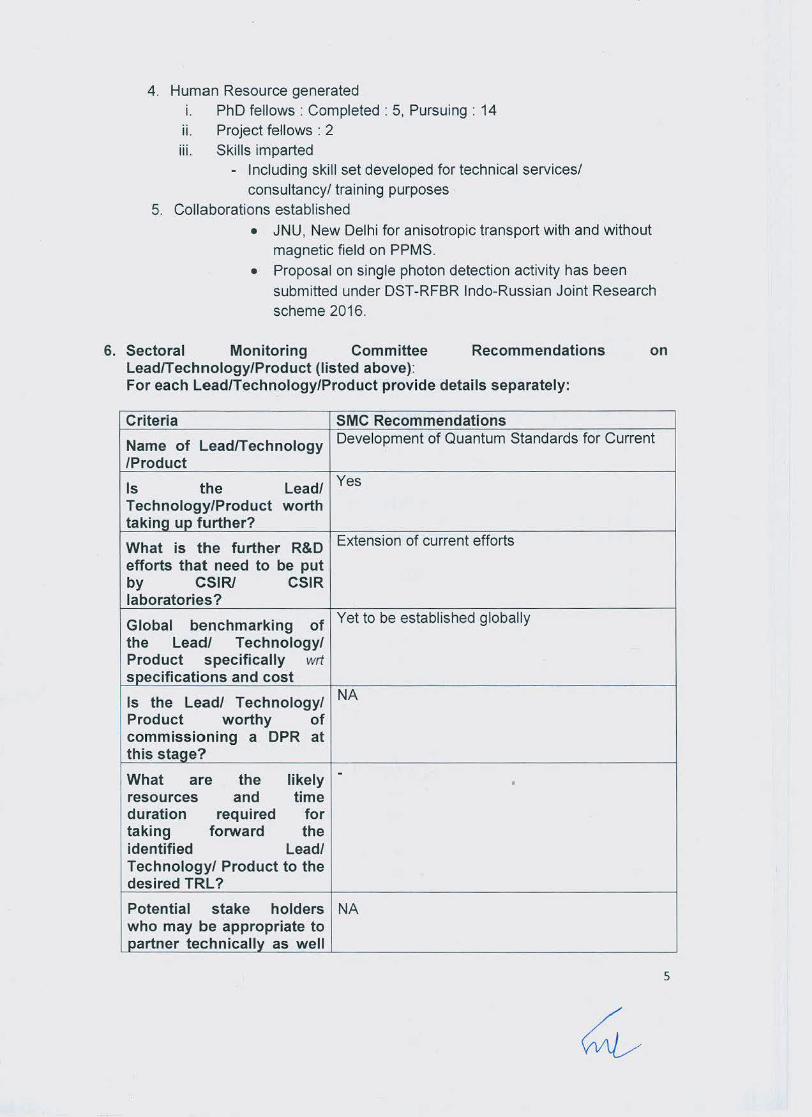
4. Human Resource generated i. PhD fellows : Completed : 5, Pursuing : 14 ii. Project fellows : 2 iii. Skills imparted
- Including skill set developed for technical services/ consultancy/ training purposes
5. Collaborations established • JNU, New Delhi for anisotropic transport with and without
magnetic field on PPMS. • Proposal on single photon detection activity has been
submitted under DST-RFBR Indo-Russian Joint Research scheme 2016.
6. Sectoral Monitoring Committee Recommendations on Lead/Technology/Product (listed above): For each Lead/Technology/Product provide details separately:
Criteria SMC Recommendations
Name of Lead/Technology Development of Quantum Standards for Current
/Product
Is the Lead/ Yes
Technology/Product worth taking up further?
What is the further R&D Extension of current efforts
efforts that need to be put by CSIRI CSIR laboratorie·s?
Global benchmarking of Yet to be established globally
the Lead/ Technology/ Product specifically wrt specifications and cost
Is the Lead/ Technology/ NA
Product worthy of commissioning a DPR at this stage?
What the likely -are • resources and time duration required for taking forward the identified Lead/ Technology/ Product to the desired TRL?
Potential stake holders NA who may be appropriate to partner technically as well
5

as financially
Suggestion for plausible -road map towards further development of lead/ technology/ product for achieving desired TRL
GO/NO GO further Go
development
Other suggestions, if any, NA
related to benefits/usage/ commercialization
7. Identified "lessons to be learnt", especially from shortcomings/failures.
8. Comments on financial progress on the project - fund availability and utilization of fund in the project: Financial progress is satisfactory and investment made is justified.
9. Sectoral Monitoring Committee Recommendations on Facility creation or other outcomes Good facility which is the base for future research leading to Quantum Standards.
10. Grading of Project Execution: Outstanding/Excellent/Satisfactory/Unsatisfactory Good
11 .Additional comments, if any: The project has resulted in quality research output. Hereon efforts should be focused on developing quantum current standards.
Signature of Chairman & all Members of Sectoral Monitoring Committee . f) A , 3 ~ ~ 'VL-
Prof. G. K. Ananthasuresh Prof Subir Kumar Saha Dr. R. K. ShJr~\{-\ C
~~-Dr. Nalin Shinghal
Dr. Aravind S. Bharadwaj
Date: 10.11 .2017
Dr. Debashis Dutta v.,
Dr. C. P. Ravikumar
Dr. S. Srikanth
~lace: CSIR-NPL, New Delhi
:>. K SH- ARMA ~ I~- r C.~Yl'ner~r , T~t.k fm-u.. \: ~~ ) .) MC) (J)y. ~ ~&. J -

Annexure I & II
Original objectives
1. Configurration of Josephson junctions for detection of weak magnetic fields, terahertz radiation and photometry (single photon counting). Measurements of magnetic quantum state in magnetic molecules and clusters at low temperatures. (WP1)
2. Understanding of the quantum phase slip processes in nanostructure·d superconductors with the objective to create devices for quantum standard of current and for counting of single photons. (WP2)
3. Fabrication of quantum structures of 20 electron gas in graphene, interfaces of oxide insulators and GaN-GaAIN heterostructures and tailoring of this quantum gas to make new devices. Studies of the novel properties of 20 electron gas at ultra low temperatures and high magnetic fielqs. (WP3)
Modified objectives
1. Fabrication and characterization of films, nanostructures and junctions of superconducting and other materials with weak magnetic field and light sensing device potential. (WP1)
2. To carry out front line quantum physics research in quantum tunneling and quantum phase slip processes with the objective to explore the possibility of creation of single photon detectors and quantum standards for electrical current. (WP2)
3. Creation and characterization of 2DEG in ultraesmall systems such as graphene and insulator oxide interfaces. The aim is to investigate the electrical transport properties of these systems at high magnetic field and low temperatures. Exploring the possibility of using the Quantum Hall Effect in these devices as the primary standard of resistance. (WP3)
7

Original Deliverables:
• Facility for clean room, development of setups for growth and characterization of Josephson Junction (JJ) based devices of conventional and exotic superconductors. Use of focused ion beam (FIB) system for nano-fabrication.
• Setups for UHV system, superconducting (SC) this film growth system. Setup facilities to measure electromagnetic response of superconducting devices at mK temperatures. Fabrication of weak link JJs, micro/nano SQUIDs and SC nanowires using FIB.
• Facility for electron beam lithography and ion-etching for wafer scale device fabrication. Stride for optimisation of specific JJ based devices. Setup facility for superconducting nanowire single photon detectors (SNSPDs)
• Fabrication of tunnel junctions and week link junctions of Nb, NbN, Mg82 and YBCO using e-beam lithography. Experiments on specific performance of superconducting devices. Fabrication of SNSPDs. Low temperature characterization SC devices in the presence of electromagnetic perturbations. Explore utility of nano/micro SQUIDs in biomedical instrumentation, magnetic field detectors and quantum standards.
• Ultra thin nanowires for study of quantum phase slip (QPS) event. Patterning to establish the basic functions of devices and low temperature study of nanowires. Quantum efficiency (QE) measurement of SNSPDs.
• Targeted fabrication of functional devices and development of new ideas/concepts to utilize the infrastructure. Low temperature experiments for understanding of QPS and single photon detectors. Development of quantum standards.
• Report generation and publication of the results, filling of patents, transfer of technologies.
Modified Deliverables:
1. Realization of Nb, NbN, MgB2 and YBa2Cu307 based superconducting nanostructures/JJs, and high quality low temperature science and feasibility of weak magn~tic field and photo sensing devices. (WP1)
2. Basic research and exploring the possibility of the development of quantum standards of current and photon counting. (WP20
3. Fabrication of quantum structures like 20 electron gas in (i) graphene and (ii) interfaces of oxide insulators and nanowires/nanoribbons of strongly phase separated oxides. Study of the novel electronic and transport properties of these low dimensional systems at low temperatures and high magnetic fields.
(WP3)
8

WP2
Continue with.other materials ·~ Con,tinued Nb and like Nb, NbN, MgB2 YBa2Cu3<i7 tz NbN superconductors with upcoming dedicated foundry
At lepst 2 JJ ·ae~_i§~s and multiple ,)J~ in supercondutting nanowires
' and meanders can·be tried
Discontinue,~fabric.atio,l't~ar)d characterization of stack:s'~of . superconducting JJs for Terahertz radiation.
~
The Qreliminary rJsults o.!l Nb thin " ~ ' ;'.,;;;._ ,;·-
film$ -QPS (Quafltuin Phase slip) devices were appreciated by the task · force. · 'Further it was recommended to let the · results
,-.,;be published in high impad f iournals. '" :,. ·
Continued with nanowlres and meanders
The recommenda'tion was considered positively; the results based .on Nb thin film QPS devic.es are published in Nature Sci. Reports.
Setups for UHV system, superconducting (SO) this'Jilm growth,sygtem.· Setup facilities to . measur:~tf!lectromagnetic response of supercqnducting devices-at mK temperatures. F;abrtcation of weak
. ,·ink JJs, micrqf nano ,SQUIDs and SC nanowires osing FlB.
Fabrication .of SNSPDs. Low temperat~f:.e characterization SC
~ ..... · d-evices in 'the presence of
Superconducting W, Nb and NbN and magnetic lianostructures
wand Graphene based w¢:ak ~ linked devices '' · "'1
_i~:;
}ft;:·f.:\
Low Temperature optica(:~ probe
Low Temperature microwave "% probes ~;1 . ~ .
and exploring of the
9