Embed Size (px)
Citation preview

PROCESS DEVELOPMENT OFBEAM-LEAD SILICON-GATE
COS/MOS INTEGRATED CIRCUITS
Final Report
9 November 1970 to 31 December 1973
JANUARY 1974
Contract NAS8-26594PRICES SUJECT TO CHANGE
Prepared By
RCA, SOLID STATE DIVISION
Somerville, New Jersey
Reproduced by
NATIONAL TECHNICALINFORMATION SERVICE
US Department of CommerceSpringfield, VA. 22151
Prepared For
GEORGE C. MARSHALL SPACE FLIGHT CENTER
MARSHALL SPACE FLIGHT CENTER
ALABAMA 35812
I(NASA-CR-120332) PROCESS DEVELOPMENT OF N742959BEAM-LEAD SILICON-GATE COS/MOS INTEGRATEDCIRCUITS Final Report, 9 Nov. 1970 -31 Dec. 1973 (Radio Corp. of America) Unclas
CSCL 09C G3/10 16763

PROCESS DEVELOPMENT OFBEAM-LEAD SILICON-GATE
COS/MOS INTEGRATED CIRCUITS
Final Report
9 November 1970 to 31 December 1973
By
B. Baptiste and W. Bosenberg
Contract NAS8-26594
Prepared By
RCA, SOLID STATE DIVISION
Somerville, New Jersey
Prepared For
GEORGE C. MARSHALL SPACE FLIGHT CENTER
MARSHALL SPACE FLIGHT CENTER
ALABAMA 35812
II

ABSTRACT
Two processes for the fabrication of beam-leaded COS/MOS integrated cir-
cuits are described. The first process utilizes a composite gate dielectrico o
of 800 A of silicon dioxide and 450 A of pyrolytically deposited Al203 as an
impurity barrier. The second process utilizes polysilicon gate metallizationo
over which a sealing layer of 1000 A of pyrolytic Si3N is deposited.
The following three beam-lead integrated circuits have been implemented
with the first process:
CD4000BL three-input NOR gate
CD4007BL triple inverter
CD4013BL dual D flip flop
An arithmetic and logic unit (ALU) integrated circuit was designed and imple-
mented with the second process. The ALU chip allows addition with four bit
accuracy. Processing details, device design and device characterization, cir-
cuit performance and life data are presented.
iii

TABLE OF CONTENTS
Section Page
I INTRODUCTION ..................... . . . . 1
II PHASE 1: DEVELOPMENT OF BEAM-LEAD SEALED-JUNCTION PROCESSING
TECHNOLOGY FOR COS/MOS CIRCUITS ......... . .... 3
A. Beam-Lead Processing of COS/MOS Circuits ........ 3
B. Metallization Process Development . ....... . . . 13
1. Process Flow . . . . . . . . . . . . . . . . . . . . 16
2. In-Process Controls ............... . 16
3. Beam-Lead Adhesion Tests . ... . . .. . . ... . . 18
C. Hermetic Seal. ...... .. . . . . . . . . . . . 18
I. MIL Capacitor Control . .. . . .... ... . ... . 19
2. Threshold Voltage Control . . . . . . . .. ... . 20
3. Hermetic-Seal Process Flow ... ......... . . 21
D. Beam-Lead Chip Separation .... . . .... ..... 29
E. Device Evaluation ......... .. . . . . . . 33
i. MIS Capacitor Measurements .... ....... . . 33
2. Threshold-Voltage and Channel-Concentration
Measurements ........... . . ...... 38
3. Life Tests . . . ...... . . . . . .. . . . . . . 45
a. Construction of Life-Test Facilities . ..... 45
b. Life-Test Schedule . . .... . . .. . . . .. 45
c. Life-Test Results ... ...... . . . ... . 50
p DC DING PAGE BLANK NOT "' v

TABLE OF CONTENTS (Cont.)
Section Page
F. Delivered Samples . .................. 58
III PHASE 2: PROCESS DEVELOPMENT OF BEAM-LEAD, SILICON-GATE
COS/MOS INTEGRATED CIRCUITS . .... ........... . 75
A. Description of the Arithmetic and Logic Unit (ALU) . . . 76
B. Silicon-Gate, Beam-Lead, COS/MOS Process . ...... . 79
1. ALU Mask Sequence . ... ... ........ . 79
2. Processing Steps ........... . ...... . 80
a. COS/MOS ................... . . 80
b. Silicon-Gate. . . . . . . . . . . . . . . . . 84
c. Beam Lead . .... ............ . . . 84
3. In-Process Controls .... ........... . 84
4. Ion-Implanted p-Wells . . .. ...... ... . . . .. 85
C. Device Characterization . ..... . ........ . . 85
1. Test Transistors . ... ............ . . . 85
2. Threshold Voltage and Channel Concentration . . . 89
3. Parameters Affecting Chip Yield ... . ... .. . . 96
D. Test-Circuit Performance ... . ........ .. . . 107
1. MOS Array Functional Testing .... . .. . . . 107
2. Propagation-Delay and Pair-Delay Measurements
on NOR Chains . ........... . . . ... ... 109
E. Yield Analysis . ...... . . . . . . . . . . . . .109
F. Life Testing . . .............. . . . . . . 116
1. Operating Life-Test Data . . . . ... ..... . . 121
2. Temperature Bias Stress ...... . . . . . . . . . 121
vi

TABLE OF CONTENTS (Cont.)
Section Page
G. Delivered Samples . ..... ....... ..... 128
IV CONCLUSIONS ........................ 133
APP. A THEORETICAL DISCUSSION OF THE METAL-OXIDE-SILICON SYSTEM . 135
APP. B STATISTICAL CHARACTERIZATION TECHNIQUE ... . .... . .. 151
vii

LIST OF ILLUSTRATIONS
Figure Title Page
1 IC Wafer After Gate-Oxide Growth .. ...... . .... 4
2 Channel Oxide Grown, and Al 20 3 Deposited . . . ....... 5
3 IC Wafer After Oxide Mask Removed by HF Etch . . . ... . . 7
4 SiO2 Etch Mask Deposited, Photolithographically Defined,
and Etched in Contact Area ........... ..... . . 8
5 Hermetic Layer Etched in Contact Layer . .... . . . . . . 8
6 Contact Area Etched Through Channel Oxide, and Si02
Etch Mask Layer Removed . . ...... ......... . . 9
7 Palladium Deposited .. . . .... . .. ....... ... 9
8 Palladium Sintered into Contact Areas, and Removed
From Oxide . . ... . . .. . . ... ... . . . 10
9 Titanium and Second Palladium Layer Deposited . . . . . . 10
10 Palladium Layer Defined into Interconnection Pattern . . . 11
11 First Layer of Gold Electroplated ....... ; . . . .. 11
12 Gold Beams Plated Up and Titanium Removed . ........ . 12
13 Beam-Lead Test Vehicle (CD4007BL) . ..... ..... . . . 14
14 Connection Diagram (CD4007BL) . ............... 15
15 Process Flow Chart for Metallization Sequence . . ... . .. 17
16 Variation of Threshold Voltage for Ranges of Effective
Channel Oxide Thickness of SiO2:A1203 and for n-Substrate
or p-Well Concentrations with Ti/Pd/Ti/Au Metal ...... . 22
SBixNO
ix

LIST OF ILLUSTRATIONS (Cont.)
Figure Title Page
17 Variation of Threshold Voltage for Ranges of Effective
Channel Oxide Thickness of SiO2:Si3N for n-Substrate
or p-Well Concentration with Ti/Pd/Ti/Au Metal . ...... 23
18 Process Flow Chart for Al203 or Si3N ..... . . 25
19 Schematic of Al203 Deposition Equipment . ......... 26
20 Schematic of Si3N 4 Deposition Equipment .. ........ . 27
21 Pellet Separation . ................ .. . . 30
22 Variation of Flatband Voltage on n and p Wafers Using
Various Composite Dielectrics: Al Metal . ......... 34
23 Variation of Flatband Voltage on n and p Wafers Using
Various Composite Dielectrics: Ti Pd Metal . ....... 34
24 Variation of Si 3 N4 /SiO 2 Flatband as Function of
Deposition Temperature . .................. 35
25 Thick SiO 2 Samples Tested at 3000C Under -10-Volt Bias . . . 36
26 Thin SiO2 Samples Tested at 3000C Under -10-Volt Bias . . . 37
27 Variation of AV with Time for Various Temperatures . .... 39
28 Threshold Voltage Change of n-MOS Units Under +10-Volt
Bias at 1250 C with Time at Temperature . ........ . . 40
29 Threshold Change of the p-MOS Units Under -10-Volt Bias
at 125 0 C with Time .................. . . 41
30 COS/MOS CD4007 Connected as Inverters for Life Testing . . . 47
31 1250C Life Testing Boards . ................ . 48
32 Environmental Test Program for CD4007, CD4000, and
CD4013 Devices ................. ..... . 49
33 Operating Life, n-Transistor Leakage Current (ILN) . . . . . 52
x

LIST OF ILLUSTRATIONS (Cont.)
Figure Title Page
34 Operating Life, p-Transistor Leakage Current (ILP) . . . . . . 53
35 Operating Life, n-Transistor Thresholds (VTN) 54
36 Operating Life, p-Transistor Threshold . . . . . . ...... . . 55
37 Operating Life, n-Transistor Output Current, IDN ...... 56
38 Operating Life, p-Transistor Output Current, IDP ....... 57
39 TC1014 (CD4000BL) Chip . . . . . . . ... . . . . . . . . . . 60
40 TC1009 (CD4013BL) Chip . .................. . 61
41 Dimensions of the TC1014 (CD4000BL) Chip . ...... . . . . 62
42 Dimensions of the TC1009 (CD4013BL) Chip . . . . . . . . . . . 63
43 Beam-Lead Packages for the CD4000 and CD4013 . . . .... .... . 64
44 Bottom View of DIC Beam-Lead Package, Type CD4000 . . . . . 65
45 DIC Beam-Lead Package, Type CD4013 ... . . ... .. . . . . 66
46 Logic Diagram of the TC1009 (CD4013BL) . ....... ... . 67
47 Functional Test Sequence for the TC1014 (CD4000BL) . . .. . 70
48 Distribution of Leakage Currents at V = 10V of
TC1014 (CD4000BL) Delivered Samples . . .. .. . .. ... .. 71
49 Distribution of Leakage Currents at VSD = 10V of
TC1009 (CD4013BL) Delivered Samples . . . . ........... 71
50 Distribution of Drain Currents at VSG - 5V; VSD = 0.5V of
TC1014 (CD4000BL) Delivered Samples ........... . . . . 72
51 Distribution of Drain Currents at VSG = 5V; VSD = 0.5V of
TC1009 (CD4000BL) Delivered Samples . ..... . .... .. . 72
52 Distribution of Drain Currents at VSG = 10V; VSD = 0.5V of
TC1014 (CD4000BL) Delivered Samples . . . . . . . . . . ... . 73
xi

LIST OF ILLUSTRATIONS (Cont.)
Figure Title Page
53 Distribution of Drain Currents at VSG = O1V; VSD = 0.5V of
TC1009 (CD4013BL) Delivered Samples ... ........... 73
54 ALU (TCC-049A) Logic Schematic Showing Cell Organization . . .. 77
55 Photograph of ALU (TCC-049A) ........ . . . ... . . . . 78
56 Self-Aligned Silicon-Gate Beam-Lead Process . ......... 81
57 Profile of Self-Aligned Silicon-Gate Beam-Lead Process ... . . . 82
58 Theoretical Plots for Ion-Implanted Well . ........... 86
59 Well-Surface Variation .............. . . . . . . . 87
60 Well-Surface Variation . . . . . . . . . . . . . . . . . . . . . 88
61 Typical Curve Display of Aluminum Metallized p-MOS
Transistors ............... .. . . . . . .. . . 90
62 Typical Curve Display of Beam-Leaded p-MOS Transistors . . . . . 90
63 Typical Curve Display of Aluminum Metallized n-MOS
Transistors ................. . .. . . . . . . . 91
64 Typical Curve Display of Beam-Leaded n-MOS Transistors . .... 91
65 Stained n-MOS Test Transistor with Polysilicon Gate and All
Oxides Removed; L (Effective) 0.20 Mil; Effective Gate
Width 2.35 Mils .................. ..... . 92
66 Stained p-MOS Test Transistor with Polysilicon Gate and
All Oxides Removed; L (Effective) 0.22 Mil; Effective
Gate Width 2.35 Mils . . ............... . . .... . 92
67 Variation of VN N as a Function of the Alloy-Anneal Time
for an n-MOS Test Transistor ...... . .......... . . . 93
68 Variation of the K-Factor as a Function of the Alloy-Anneal
Time for an n-MOS Test Transistor . ........... . .. 94
xii

LIST OF ILLUSTRATIONS (Cont.)
Figure Title Page
69 Typical Leakage Distribution on Wafer - All Chips . ..... 108
70 Tapered Stepped Oxide ................... . . 113
71 Standard Stepped Oxide ................. . . . 113
72 SEM.Detail of Beam-Lead Metal Crossing Over Polysilicon . . . 114
73 SEM of a Portion of ALU Chip Showing Beam-Lead
Interconnect Metal Crossing Polysilicon Lines . . ..... . 115
74 SEM Detail Showing Beam-Lead Metal-To-Polysilicon Contact . 115
75 n -p+ Diode Resulting from Enlarged Stepped-Oxide Mask and
Undercut Doped-Oxide Mask . .... . . . . ....... . . . 117
76 n Source Diffusion Shorting Out p Guard Band. . ... . . . 118
77 TCC-049 Level-One Mask (Well) ................ . 119
78 Bias Life-Test Circuit for TCC-049A Test Transistors ..... 120
79 Initial Life Data from TCC-049A Test Transistors ...... . 122
80 CVBT Curves of p+ Doped Polysilicon p-MOS Test
Transistor Gates . . . . . . . . .......... ... ... 123
81 CVBT Curves of n+ Doped Polysilicon n-MOS Test
Transistor Gates .......... .. .. ....... . . . 124
82 CVBT Curves of p+ Doped Polysilicon p-MOS Test
Transistor Gates . ............ .... .... . . . 125
83 CVBT Curves of n Doped Polysilicon n-MOS Test
Transistor Gates . . . . . ... .. . . . . . . .... 126
84 Packaged TCC-049A Chip . .... ...... . . .. . . 130
85 Pin-Out Data for the TCC-049A Chip . . ......... . 131
xiii

LIST OF TABLES
Table Title Pae
I Hermetic Seal-To-Channel Oxide Thickness Ratios . . . . ... . 19
II Design Parameters for SiO2 :Al 0 3 (IVtl = 1.2V) . . 24
III Threshold Voltages for Ideal Interfaces (Nss = O)
of A1203:SiO2 Gates ..... ... ...... . . . . . . 24
IV Primary Data for Typical n-MOS and p-MOS Transistors with
Composite Gate Dielectric. . . . . . . . . . .. . . . . . 42
V Calculated, Zero Current, Threshold Voltage as a Function
of Substrate Bias and Statistical Block Size for n-MOS andp-MOS Transistors of Preceding Table . . .. . . . . . . . . . 43
VI Calculated Channel Concentration as a Function of the
Statistical Block Size for n-MOS and p-MOS Transistors of
Preceding Tables. (Computation Errors Increase for the
n-MOS Transistors with Decreasing Differences of
Substrate Bias.) . . . . ... . ... ....... 44
VII Summary of (Extrapolated) Threshold Voltages (Vt), Channel
Concentration (N), Surface State Densities (Nss), and
Threshold Voltages for Zero Surface State Densities for
TC1010 Lot 219 . ............... .. . . . . 46
VIII Test Program for TC1014 (CD4000BL) . . . . . . . . . . . . . . 68
IX Test Program for TC1009 (CD4013BL) . .. . . .... . . . 69
X Room-Temperature Raw Data of Needed Gate/Drain Voltage
to Achieve Drain Currents from 1 to 625 Microamperes ... . 97
XI Extrapolated Threshold Voltage for Six Statistical
Block Sizes . . . . . . . . . . . . . . . . .. .98
V'~c%~

LIST OF TABLES (Cont.)
Table Title Page
XII K-Factor as a Function of Statistical Block Size . ...... 99
XIII Complement of Correlation Coefficient in Parts Per
Million (PPM) as a Function of Statistical Block
Size and Substrate Bias .. ................ . . 100
16 -3XIV Channel Concentration (in 10 cm ) for n-Polysilicon-Gate
n-MOS Transistors as Calculated from Eq. (13), Appendix B . . 101
15 -3XV Channel Concentration (in 10 cm ) for p-Polysilicon-Gate
p-MOS Transistors as Calculated from Eq. (14), Appendix B . . 101
XVI n-Substrate Resistivity as Calculated from Table XV . .... 102
XVII n-MOS Test Results of Past Processed Lots . ........ . 103
XVIII p-MOS Test Results of Past Processed Lots . ........ . 104
XIX Typical n-MOS Test Transistor Parameters - Recently
Processed Lots . ... . . . . .... . . . . . . . . ... 105
XX Typical p-MOS Test Transistor Parameters - Recently
Processed Lots . .................. . .... 106
XXI Performance of the NOR Gate with Pair Delay . ... ...... 110
XXII Performance of the Five-Stage NOR Gate with
Propagation Delay ................... ... 111
XXIII Test Transistor Data Showing the Process Parameters
that Affect Speed ......... . . ...... .. . . 112
XXIV Temperature Bias Stress Data .. ... . ... .......... . 127
XXV Test-Transistor Data of Delivered TCC-049A Samples
from Lot 39C ........ .......... . ... . .. 129
xvi

SECTION I
INTRODUCTION
In order to fabricate reliable COS/MOS integrated-circuit logic and memory
chips that can be interconnected on a small substrate to form a variety of sub-
systems, beam-leaded chips are mandatory. Unfortunately the normal bipolar
beam-lead process, whose worth has been proven on life and stress tests over
the years, cannot be applied directly to.COS/MOS devices. The more severe re-
quirements for the use of the hermetic seal in MOS processing require additional
development. In addition, the standard sputtering process used in bipolar de-
vice processing introduces charge into the gate oxide which cannot be removed
by annealing. Both of these cause the threshold voltages to wander from device
to device and to be unstable. For these reasons variations have been introduced
from the standard bipolar beam-lead process to solve these problems. The general
philosophy guiding such variants, however, is that they be few, and that the pro-
cess itself be kept as close to the standard beam-lead scheme as possible. It
is hoped that by following such a procedure, the long-term documented bipolar
life-test data may be applicable to COS/MOS beam-lead devices.
The work was performed in two phases. Section II of this report covers the
work with conventional non-self-aligned metal gates over a composite gate
dielectric of Si02:A203. The aluminum oxide layer is used for sealing the
critical gate dielectric from sodium penetration. Section III of this report
covers the work with self-aligned polysilicon gates that are sealed by a much
heavier layer of silicon nitride. In both cases an identical metal system for
the beam leads has been used that allows deposition by evaporation.

SECTION II
PHASE 1: DEVELOPMENT OF BEAM-LEAD SEALED-JUNCTION PROCESSINGTECHNOLOGY FOR COS/MOS CIRCUITS
A. BEAM-LEAD PROCESSING OF COS/MOS CIRCUITS
The beam-lead approach followed in this program differs from the standard
bipolar type of beam-lead process in only two particulars:
a. -The hermetic seal, Al203 that is placed between the gate oxide
and the metallizatiod must be deposited clean. Any deviation of
the flatband voltage of the deposit from theory, whether due to
interfacial charge, ffiobile charge, or potential discontinuities,
will shift the device thresholds. These shifts must be avoided
so that reasonably matched and stable thresholds are obtained.
In bipolar beam leading, few or no controls are needed on the-
silicon nitride.
b. The metallization used is Pd2Si-Ti-Pd-Ti-Au instead of PtSi-Ti-
Pt-Ti-Au. This change is made to avoid the necessity of sput-
tering which introduces charge and, hence, threshold shifts into
the devices. Palladium can be evaporated with standard equipment.
The process being used at RCA to fabricate beam-lead devices is as follows:
a. The IC wafer is processed normally by using the well known stand-
ard COS/MOS process until the gate oxide growth step has been
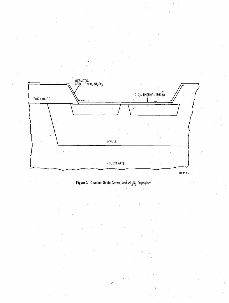
completed (topologically depicted in Figure 1).
ob. Immediately after the 800 A SiO 2 film has been grown, the wafer
is placed in an aluminum oxide deposition chamber in which a0 o
400 A film is deposited at 850 C. The deposition time is ap-
proximately 4 minutes. The layer acts as the hermetic seal,
protecting the devices not only from the environment, but even
more importantly from future processing contamination (see
Figure 2).
PRBCEDING PAG BLANK NOT F~LME 3

rin
C
05239L
Figure 1. IC Wafer After Gate-Oxide Growth
HERMETICSEAL LAYER, A120 3
Si02, THERMAL (800 A)THICK OXIDE
ni
p WELL
nSUBSTRATE
03917L
Figure 2. Channel Oxide Grown, and A1203 Deposited
5

0c. A 3000 A oxide is deposited over the wafer to act as an etchant
mask. Photoresist is applied and contact holes are etched into
the oxide mask. The wafer is etched in phosphoric acid, which
removes the Al20 3 covering. The wafer then is etched with buffer
HF to open the contact holes in the underlying Si02 to sources,
drains, and substrate contacts. The oxide mask also is removed
during the HF etch. The topology is shown in Figure 3, and
Figures 4, 5, and 6 depict the sequential cross sections.
od. A 500 A layer of palladium is evaporated over the wafer and then
sintered at 4500C for 30 minutes. This causes the palladium and
the silicon in the contact windows to react and form palladium
silicide for the ohmic contact. The palladium over the hermetic
seal is etched off (see Figures 7 and 8).
o oe. Next, layers of 1500 A titanium and 1500 A palladium are con-
secutively evaporated over the wafer. A photoresist beam-lead
metal-mask operation is performed and the metal pattern is
defined in the palladium layer. The etching stops at the
titanium layer so that the titanium layer can be used for cur-
rent carrying in the subsequent plating operations, since it
covers the entire substrate (see Figures 9 and 10).
f. A photoresist negative metal-mask operation is next employed so
that only the metallization is exposed to the ambient. The wafer
is placed in a gold plating bath and a 1.5-micrometer layer of
gold is plated in the exposed regions (see Figure 11).
g. A photoresist operation next opens up the beam areas and a 12-
micrometer gold layer is plated over the beam pads using the
photoresist as the plating mask.
h. The titanium layer is etched open with the gold pattern acting
as the etch mask (see Figure 12).o
i. A protective 10,000 A layer of SiO 2 is deposited over the wafer
and opened at the beams. The oxide is deposited from silane at
250 0C.
6

05240L
Figure 3. IC Wafer After Oxide Mask Removed byHF Etch.
7

HERMETICLAYER, Al20 3 oSi0 2 SiO MASK (3000 A DEPOSITED)
THICK OXIDE
+n+7
pWELL
n SUBSTRATE
03916L
Figure 4. Si0 2 Etch Mask Deposited, Photolithographically Defined, and Etched in Contact Area
THICK OXIDE
n+ n+
pWELL
n SUBSTRATE
03919L
Figure 5. Hermetic Layer Etched in Contact Layer
8

P WELL
n SUBSTRATE
03920L
Figure 6. Contact Area Etched Through Channel Oxide, and SiO 2 Etch Mask Layer Removed
PdTHICK OXIDE J 7
p WELL
n SUBSTRATE
0392 1 L
Figure 7. Palladium Deposited
9

pWELL
HERMETIC SUBSTRATE
03922A203
Figure 8. Palladium Sintered into Contact Areas, and Removed From Oxide
THICK OXIDE
p WELL
n SUBSTRATE
03922L
Figure 9. Titanium and Second Palladium Layer Deposited
1010

p WELL
n SUBSTRATE
03924 L
Figure 10. Palladium Layer Defined into Interconnection Pattern
THICK OXIDE
p WELL
n SUBSTRATE
03925L
Figure 11. First Layer of Gold Electroplated
11

n+ Pdi 1n+
p 'ELL
n SUBSTRATE
10,000 A
10,000 A
SCALE03926L
Figure 12. Gold Beams Plated Up and Titanium Removed
12

j. The wafer is backlapped to 5 mils, back coated with photoresist,
and the streets are opened up. The silicon grid is etched through
to the beams, thus separating the pellets.
The result of these operations is the beam-leaded sealed-junction COS/MOS
chip shown in Figure 13. The photograph is of a beam-lead, sealed-junction
version of the RCA CD4007, used as the test vehicle in the early stages of
process development. The connection diagram for the CD4007BL is illustrated in
Figure .14. The CD4007 was chosen because the three n and three p transistors
can be accessed individuhlly and the beam-leaded devices can be studied in
detail and the process and any process changes can be readily evaluated. These
devices are measured both on curve tracers qualitatively and on a computer-
controlled test set statistically. Subsequent designs have been using two
n-MOS and two p-MOS transistors with thin and thick gate oxide in the perimeter
of the integrated circuit. Appendix A details the statistical technique utilized
in determining these parameters. The parameters measured for both n- and p-
type transistors include:
a. Threshold voltage (VTh) at IDS = 10 microamperes.
b. Drain-to-source leakage current (IDSS) at IVDS = 10 and 17 volts.
c. DC forward transconductance (gfs) at IVGSI = 10 volts and VDSI= 3 volts.
d. Gate leakage (I G ) at IVGSI = 10 and 17 volts.
In addition, the p- and n-drain contact-resistance leakage currents between
the n substrate and the p well are measured and a set of 12 continuity tests
are made.
B. METALLIZATION PROCESS DEVELOPMENT
Although many areas for potential improvement, process simplification, and
increased reliability remain, the process developed has proven to have a good
yield and, as will be seen, produces very stable devices.
The metallization system evaporator includes rotating domed planetary sub-
strate fixturing and a completely self-contained control.system for the evap-
13

888
iiits
14 13 1205080V
Figure 13. Beam-Lead Test Vehicle (CD4007BL)
14

14 2 11
PP p
6 13 3 1 100o -- - 128 5
7 4 9
05081 L
Figure 14. Connection Diagram (CD4007BL)
15

oration and monitoring of the Ti and Pd thin films. The fixturing will ac-
commodate up to 28 2-inch wafers. Runs have shown good film uniformity with
thickness running within ±5 percent variation within a run.
I. PROCESS FLOW
Using the CD4007BL devices as test vehicles, a metallization process was
defined. The process flow chart is shown in Figure 15.
While the processing outlined is self-explanatory, the following points
bear a more fully detailed discussion.
a. The palladium sintering operation can take place at any temper-
ature in the 4000C to 6000 C range. The time duration is on the
order of 15 to 40 minutes.
b. In the wafer cleaning operation, a critical process step exists
between ensuring cleanliness and low contact resistance. Over-
cleaning in HCI can remove part of the Pd2Si contact, while un-
dercleaning often results in high leakages.
c. Titanium must be evaporated at the lowest possible pressure,
otherwise a titanium oxide is formed and this results in lift-
ing of the metal pattern after definition.
d. An iodine-based commercial etch is used for the interconnect
pattern. This palladium etch reacts with the titanium under-
layer and colors it. This coloration shows when the palladium
layer has been defined over the wafer and thus eliminates the
problems of either overetching (undercutting) or underetching
(metal bridging).
2. IN-PROCESS CONTROLS
Major emphasis is given to controls on the following items:
a. Palladium thickness is measured during evaporation by a quartz
crystal oscillator and after evaporation by either a Talysurf
or an interference microscope. This control is essentially
single-ended, having a lower limit specification only.
16

VISUAL MEASUREINSPECTION Pd
THICKNESS
CONTACTS PALLADIUM PALLADIUM STRIP REMOVE
OPENED EVAPORATION SINTER H IHERMETIC TRACES. CLEAN 'iPd
2 Si) SEAL Pd
MEASURETHICKNESS VISUAL
DURING INSPECTIONEVAPORATION MASK 7
MASK 6 (REVERSE OFMASK 6)
DEFINEEVAPORATE INTERCONNECT TCDEFINE
A INTERCONNECT PATTEsRN PAL UM et PLATEMETAL PRPALLADIUM PL L
CONTACT MEASURE
RESISTANCE TOTAL
MEASURE THICKNESS(AFTER)
VISUAL
MASK 8
DEFINE PLATE ETCHSGOLDII GOLD TITANIUM TO CIRCUIT
PLATE BEAMS INTERCONNECT PROBE TESTING
05546L
Figure 15. Process Flow Chart for Metallization Sequence

b. The Ti:Pd thicknesses are similarly monitored. The total thick-
ness is greater than twice the thickness of the channel oxide to
ensure that the contact holes are completely metal filled.
c. After palladium definition, the visual inspection is keyed at
maintaining an overlap of the interconnect metal to the contacts
to prevent the subsequent gold plate from entering the contact
region and reaching the silicon itself.
d. After etching the titanium, particular attention is paid to make
sure that etching of the regions between source-gate and drain-
gate metal lines is complete.
3. BEAM-LEAD ADHESION TESTS
A series of CD4007 devices were beam-lead bonded to a 14-lead DIC fashioned
such that the chip was over a 40-mil hole in the ceramic. This permitted the
use of the push-off test, in which a rod is pushed through the hole against the
bonded chip. Pressure is gradually applied and the point at which the bonds
fail is measured.
All chips exceeded the 20-gram specification and some exceeded the 100-
gram limit of the apparatus.
C. HERMETIC SEAL
At the beginning of the program silicon nitride and aluminum oxide were the
two dielectrics considered for sealing the critical MOS gate. Silicon nitride
is more impervious to sodium than aluminum oxide and has a lower conductance.
Both dielectrics are deposited at high temperatures in reactors that are in-
ductively heated. Both dielectrics gave good seals and electronic properties
that allowed MOS transistor threshold voltages in the range of 1 to 2 volts by
adjusting the processing. Since there is a negative charge introduced at the
A1203 :Si 2 interface (and zero charge for Si3N4 :Si0 2), it was easier to adjust
the p-MOS to a low threshold voltage with Si02:A1203. For this reason Al203 was
chosen over Si3N .
18

1. MIS CAPACITOR CONTROL
Metal-insulator-silicon capacitors have long been used to characterize
semiconductor surface properties. The high-frequency capacitance equals the
insulator capacitance (with an effective thickness teff) under heavy accumu-
lation, and reduces to a lower value under inversion. The voltage at which
this transition occurs is called the flatband voltage since no band bending in
the silicon-band structure occurs. The stability of the structures has been
tested at 3000 Cfor 1 minute under +10 and -10 volt biases (106 volt/cm).
This way test matrices with various ratios of gate dielectric 1 to gate di-
electric 2 have been tested, see Table I.
TABLE I. HERMETIC SEAL-TO-CHANNEL OXIDE THICKNESS RATIOS
Silicon Nitride Matrix Aluminum Matrix
Thicknesses (A) Thicknesses (A)
Si02 Si3N4 Si02 Al203
1000 0 1000 0
800 380 800 450
600 700 600 900
400 1050 400 1350
200 1400 200 1800
The effective thickness, teff, of the gate dielectric is
ESiO
t =t +t ....... ................... (1)eff SiO seal seal
and has been kept at 1000 A, a value allowing for enough margin to prevent pre-
mature gate breakdown (SiO = 3.82; Al203 = 9.5; ESi3N = 6.9).
2 2 3 3419
19

2. THRESHOLD VOLTAGE CONTROL
The threshold voltage is usually expressed as
qN 2q SiE N 2V(+It C C 2Vf +Vsub ± Vf + % .MS (2)
ox ox
use + sign for n-MOS
use - sign for p-MOS
where
SiO_ oC = oxide capacitance =ox teff
N = carrier concentration in the channel
N = interface state densityss
0MS = metal-semiconductor work function
Vsub = substrate voltage
V = Fermi voltage
Vt = threshold voltage at Id = O
The presence of Si3N or Al203 in the gate structure influences the thres-
hold voltage in two ways. First, the interface charges in the Si3N4 or Al203/SiO2 interface will be reflected as effective surface-state concentrations,
N s, in the Si02/Si interface, and a lower work function, MS Second, the
effective channel thickness, t, is modified by the dual dielectric.
The effective 4MS (including ii) for the Si02:A203:Ti:Pd:Au system is
approximately 0.55 eV lower than that of n silicon, while the corresponding
value for the Si0 2 :Si3N :Ti:Pd:Au system is approximately zero. The surface-
state densities on (100)-silicon are approximately:
10 -2 11 -2Nss = 7 x10 cm for n-MOS; N = I x 10 cm for p-MOS with Al 203
N 11 -2 10 -2ss = 1 x 10 cm for n-MOS; N = 8 x 10 cm for p-MOS with Si Nss 3420
20

The threshold-voltage-concentration design curves are plotted in Figures16 and 17. As can be seen from Figure 17, p-MOS transistor threshold voltagesbelow 1 volt cannot be obtained with SiO2:Si3N . On the other hand, the sep-aration between the n-substrate and p-well concentration (overdoped.by diffu-
sion) is much larger, making this diffusion easier when compared to the SiO 2:Al203 system. Since MOS circuits run faster (at a given supply voltage) withlower threshold voltage, it was decided to use the SiO :Al103 system. The
o o 2 2 3process was stablized with 800 A of SiO2 and 400 A of Al203, corresponding toan effective insulator thickness of about 1000 A.
For SiO2:A1203, the set of parameters in Table II can be used. Since a
light p diffusion is used for the n-type MOS, the ratio of surface-to-bulkconcentration is somewhat low. A slight mismatch in threshold voltages that
does not affect circuit performance might be more desirable.
A final consideration on low-threshold design is the effect of surface-
state desnity on thresholds. In the foregoing analysis, a surface-state den-
sity that calculates out to a -0.47 volt potential for the p-M OS and one of-0.33 for the n-MOS was assumed (for t = 1000 A), as shown in Table III.
oxThis value appears reasonably constant.
3. HERMETIC-SEAL PROCESS FLOW
The process for fabricating the alumina-silica and the silicon-nitride-
silica gate dielectric was defined and the process flow is given in Figure 18.
oAfter a clean 800 A SiO2 film has been grown, the wafer is transported to
the alumina or silicon nitride deposition system. This particular apparatus
consists of series of four round silicon carbide-coated carbon susceptors eachhaving a carbon shaft whose end point is affixed into a revolving quartz tubeas shown in the schematic of Figure 19 for the Al203 deposition and Figure 20for the Si3 4 deposition. The susceptors rest upon a second quartz tube, whichis larger in diameter but concentric with the first tube. Revolving the quartztube causes the susceptors to rotate and due to friction with the outer quartzthey also rotate. This planetary arrangement assures uniform heating of thesusceptors in the RF field generated by the concentric RF coil outside the
21

1017
n-MOS Transistors
Nss = 7x1010 cm-2
1016
p-MOS Transistors
Nss= 1x1011 cm-2
1014
-0.5 0 0.5 1.0 1.5 2.0 2.5 3.0
IVt (volts) ---- P 06649L
Figure 16. Variation of Threshold Voltage for Ranges of Effective Channel OxideThickness of Si02 : A1203 and for n-Substrate or p-Well Concentrationswith Ti/Pd/Ti/Au Metal
22
0 /- "a,/
caL
22

1017n-MOS Transistor
Nss= lx1011 cm-2
1016
o
CL p-MOS Transistor
-C3 INss 8xI010 cm-2
1014
-0.5 0 0.5 1.0 1.5 2.0 2.5 3.0
I Vt I(volts) ' 0665OL
Figure 17. Variation of Threshold Voltage for Ranges of Effective Channel Oxide Thicknessof Si0 2 : Si3N 4 for n-Substrate or p-Well Concentration with Ti/Pd/Ti/Au Metal
23

TABLE II. DESIGN PARAMETERS FOR SiO 2 :Al 2 0 3 (IVtl = 1.2 V)
p-MOS n-MOS
Substrate Concentration 1.22 x 10 15 7.30 x 10¹⁵
o oSiO 2 Oxide Thickness 800 A 800 A
o oActual Composite Thickness 964 A 964 A
"Corresponds to 4.02 ohm-cm of n silicon
TABLE III. THRESHOLD VOLTAGES FOR IDEAL INTERFACES
(N = 0) OF Al 203:SiO 2 GATES
V tp(Volts) Vtn(Volts)
n-substrate resistivity in ohm-cm p-well concentration in cm-3
15 15 16 161 2 3 5 10 5.0 x 10 9.0 x 10¹⁵ 1.5 x 10 3.0 x 10
1000 -1.36 -1.00 -0.85 -0.70 -0.55 1.33 1.71 2.16 2.98
24

CV-BTTEST
WAFER
MASK 5
FROM DEPOSITIONFROM 450 of A1203 ANNEAL Si02 CONTACTGATE or 450'C DEPOSITION PHOTOOXIDE 380 of Si3N4 3000 KTFR(800 A)
VISUAL
VISUAL VISUAL INSPECTION VISUALINSPECTION INSPECTION INSPECTION
ETCH ETCH REMOVE ETCHGUIDE A203o r REMOVES
o Si3N 4 S-i-* -
(00 A) (3000 A)
TO oses05859L
METALLIZATION
Figure 18. Process Flow Chart for A1203 or Si3N4

EXHAUST
i MIXINGCHAMBER
oUILb Il * oU " * *:***COILS
o * - *o: VAC
OVEN
*:
=Q: HEATED I
=C 2
D :C02 05857L
Figure 19. Schematic of A1203 Deposition Equipment

EXHAUST MIXINGCHAMBER
RF 0 0 0COILS OO
" r
S=N 2 =NH 3
-= SiH4
06651 L
Figure 20. Schematic of Si3N 4 Deposition Equipment

reaction chamber. The silicon wafers are placed upon the ledges inset into
the susceptors. Since the susceptors are tilted, the slices do not fall off
during rotation and make contact with the susceptors over their entire area
ensuring good thermal contact and uniform heating.
By adjusting the RF generator output power, the susceptors and slices are
heated to 8500C in a hydrogen atmosphere. At this point, carbon dioxide is
introduced into the chamber causing the formation of water vapor by the reac-
tion
8500 C
H2 + CO2 1 H20 + CO
Since this reaction occurs only at temperatures above 7000C, these products
are formed only near the heated susceptors. A minute after the carbon dioxide
is introduced, the hydrogen flow line through the aluminum chloride sublimator
is activated and aluminum chloride enters the chamber. The sublimator holds 1
pound of powder heated to 1100C over which the hydrogen is directed in a
labyrinthian manner.
The chemical reacts with the water vapor near the susceptors to form the
oxide. This is expressed as
2 A1Cl3 + 3 H20 - Al203 + 6 HC1
o oA deposition rate of 100 A/minute is normal; when it drops below 80 A/minute,
the system is overhauled (approximately every 6 months).
The relative amounts of reagents in this process are:
Flow Rate
Reagent (Liters/Minute) Percentage
H2 10 99
CO2 0.08 0.72
H2 (through the A1Cl3 chamber) 1 0.036 of A1C132 .3 3
The aluminum oxide layer is etched with phosphoric acid at 180 0C. Because
photoresist cannot take such treatment, a secondary mask is required. For
28

0
this case a thick masking oxide of about 3000 A is deposited. This is opened
up with the contact mask. This oxide then acts as a mask to open up the
aluminum oxide portion of the contact during the phosphoric acid etch.. The
aluminum oxide then acts as a mask during the opening of the silica portion
of the contact in the contact-etch sequence. The masking oxide is removed
simultaneously with the silica contact opening by the action of the buffered
hydrofluoric acid etch.
For Si3N , the susceptor and the silicon slices are heated to 10500C in a
nitrogen atmosphere. At this point ammonia is introduced into the chamber.
After 15 seconds silane is introduced and silicon nitride is deposited by the
following reaction
1050 0C3 SiH + 4 NH3 Si3N + 12 H2
Since this reaction occurs only at temperatures above 7000C, these products are
formed only near the heated susceptor. A deposition rate of 100 A/minute is
normal. The relative amounts of reagents in this process are:
Flow Rate
Reagent (Liters/Minute) Percentage
N2 10 80.3
NH 2.1 16.9
3% SiH4 in N2 0.35 2.8-3
(10.5 cm /minute ofpure silane)
D. BEAM-LEAD CHIP SEPARATION
Since the devices being manufactured are interdigitated beam-lead types,
the pellets cannot be separated simply by scribing as standard-processed pel-
lets are. For separating beam-lead chips (one from another) a more complex
but more reliable and higher yielding process is the back-lapping etch process.
The process sequence for the transferring and bonding operations are shown in
A, Figure 21. The details of the back-lapping etching process are illustrated
in B, Figure 21. Following is a description of the separation process:
29

MEASURETHICKNESS
YIELD
ACCEPT MOUNT ON BACK PHOTOSAPPHIRE GRIND RESIST
RECEIVE WAFERSFROM MEASURE ON
TAC PROBEFINAL METALLIZATION
REJECTINSPECT
SEPARATION DISSOLVEBIWAX
TO REPROCESS
S EXPOSE TEST TRANSFERSDEVELOP & DRY INK TO
& ETCH Si INK MESH
DISSOLVENITROCELLULOSE
TRANSFER WOBBLE-BONDTO TO FINAL TEST
LUCALOX PACKAGE
05856LA. PROCESS SEQUENCE FOR TRANSFERRING AND BONDING OPERATIONS
Figure 21. Pellet Separation (Sheet 1 of 2)

SILICON Au BEAM (12/ m)SILICON ANCHOR PAD
0.015" REGION BEAM REGION BIWAX
SAPPHIRE DISC
A. MOUNT SILICON WAFER ON SAPPHIRE DISC
0.002-0.003"
SAPPHIRE DISC
B. BACK GRIND WAFER
0.002-0.003"
PH OTORESIST PHOTORESIS
SAPPHIRE DISC
C. BACK ALIGN
HF-ACETICSILICON HN03
SAPPHIRE DISC
D. BACK ETCH058561L
B. STEP.BY STEP BACK-LAP PROCESS
Figure 21. Pellet Separation (Sheet 2 of 2)
31

a. The wafer is sample circuit probed and the yield projected.
b. Wafers having a satisfactory yield are waxed face down to either
a sapphire or Lucalox disc. The disc is usually about 35 mils
thick, is transparent and has a diameter 1 inch larger than the
silicon wafer. The wax employed is Biwax.
c. The wafers, which are about 11 to 14 mils thick, are back ground
to about 4 to 5 mils (depending on the chip size).
d. After back grinding, the wafers are photoresist coated on the
back side (silicon surface), and aligned to the separation mask
by back alignment. This alignment employs infrared light which
transmits through the silicon layer and is absorbed by the metal
patterns, thus permitting alignment to the mask. The photoresist
(negative type) is exposed in the usual manner and developed.
e. After exposure, the wafers are etched in a hydrofluoric, acetic,
and nitric acid solution until the anchor pads on the beam leads
are exposed.
f. The wafers are 100-percent tested against the full range of
specifications and the defective chips inked. The ink is then
baked on.
g. Upon inking, the transferal operation is begun. The wafer and
disc are glued onto a stainless steel mesh with a mixutre of
nitrocellulose and acetone.
h. After glueing, the Biwax is dissolved with trichloroethylene from
the sapphire disc and the back of the silicon, leaving only the
chips on the screen.
i. A Lucalox disc, coated with silastic S2288, is pressed against
the array of chips and then the nitrocellulose is dissolved
away in acetone.
j. The chips on the silastic-coated Lucalox are picked up by the
bonding tool and wobble bonded down to the ceramic substrate
as required.
32
E. DEVICE EVALUATION
1. MIS CAPACITOR MEASUREMENTS
As mentioned in paragraph C several matrices were set up to study the flat-
band voltage and its shift under stress of MIS capacitors having various ratios
of SiO2 and Al203. The deposition temperature was also varied in a systematic
way to obtain optimized conditions. The flatband voltages of each wafer were
determined by using both Al and TiPd.metals. Both n and p silicon wafers were
tested. The results are shown in Figure 22 for Al and Figure 23 for TiPd.
The graphs show that a 0MS difference of above 0.3 volt exists between Al and
TiPd.
A second matrix involved studying the flatband voltage of silicon nitride
sandwiches deposited at temperatures of 800 C, 900 C, and 1050 C. The results
are shown in Figure 24. The points recorded were only of flatband voltages.
Bias temperature curves were also taken, but their deviations from flatband
voltage were only 0.1 of a volt. Although a definite variation with temperature
was found, almost the same variation was found in the Si02 control capacitors,
so that at least part of the variation was due either to the quality of the
SiO2 or to the annealing conditions.
The time dependence of the flatband-voltage shift was also studied. Figure
25 shows the shifts for both Al203 and Si3N4 for up to 3000 seconds at 3000C.
It can be seen that the two types of sandwich layers behave quite differently.
First, the alumina silica shows threshold-voltage drift under negative bias,and at some later time the silicon nitride shifts become evident. The alumina
,shift saturates around AV - 0.7 volt, but the nitride continues to increase
showing some sign of saturation near the end of the experiment. The shift of
the nitride sample can be explained by charging taking place at the interface
using the Frankel-Poole tunneling model. No such model pertains to the alumina,however.
0 oThe ratios of 800 A of Si0 2 to about 400 A of Al203 or Si N4 are more stable
than that of 200 A of Si02 to about 1600 A of Al 03 or Si3N (see Figure 26).2 2 3 3 (see Figure 26).
In either case the same situation exists, but the difference between the nitride
and the alumina is amplified. Once again the alumina saturates and the nitride
33

0
X n-TYPE Si
U -. P-TYPE Si
-2.0 I I I I I I I I
A1203 200 400 800 1200 1600o
THICKNESSES (A)
Si0 2 1000 800 600 400 20005173L
Figure 22. Variation of Flatband Voltage on n and p Wafers Using Various Composite Dielectrics:Al Metal
n-TYPE Si O0
0
0
P-TYPE Si
S-1.0
-2.0 a
A1203 400 800 1200 1600o
THICKNESSES (A)
SiO 2 1000 800 600 400 20005174L
Figure 23. Variation of Flatband Voltage on n and p Wafers Using Various Composite Dielectrics:Ti Pd Metal
34

0
-1.0
800 900 1000 110005175L
Figure 24. Variation of Si3 N4 /SiO 2 Flatband as Function of Deposition Temperature
35

2.0
0NOTE: 400A HERMETIC SEAL
DEPOSITED ON 800A SiO 2
1.5
1.0
> A1203/Si02
0.2
0
10 102 103
TIME (SECONDS)05373L
Figure 25. Thick SiO 2 Samples Tested at 3000 C Under -10-Volt Bias

I I I I I0
NOTE: 1600A HERMETIC SEAL DEPOSITEDoON 200A SiO 2
I ¢AI2O3/Si0 2 (N5A)
00
6.0 0,, -3 "
L
Si3N4/SiO 2 (N5B)
2.0 .000
10102 103
TIME (SECONDS)
05374LFigure 26. Thin SiO2 Samples Tested at 3000C Under -10-Volt Bias

shifts are small for short test times. The increase of threshold with time
can again be explained by charging at the interface. It should be noted that
while some of these shifts seem severe, the test temperature is so high that
shifts at room temperature may be immeasurably small and it might be many years
under bias before the threshold shifts become noticeable. How important this
problem is will depend upon its activation energy. Obtaining this information
is not a simple matter as can be seen from Figure 27, which shows the variation
of flatband with time for various heat-treatment temperatures. The sample
shown was the least stable of the lots tested.
The high-temperature (3000C) stress tests have been correlated to 1250 C
operating-life data. The total time span was 3000 hours. Figures 28 and 29
show the shift in threshold voltage with time. The n-MOS transistors with
Si3N4 show initially slightly less shift, reducing the threshold voltage, while
those with Al203 increase the threshold voltage. In either case the total shift
is approximately 0.15 volt at 3000 hours. The n-MOS transistors with Si3N 4seem to have a larger slope of change in threshold voltage at the end of the
testing period. The p-MOS transistors in Figure 29 show that the Al203 units
are far more stable than the Si3N units, showing decreases in threshold voltage
of about 0.1 and 0.4 volt, respectively.
2. THRESHOLD-VOLTAGE AND CHANNEL-CONCENTRATION MEASUREMENTS
A statistical technique that is described in Appendix A has been used to
characterize the MOS transistors precisely. The threshold voltage is obtained
by extrapolation through a least square fit of VF - V data points. These
data are also measured (on automatic test equipment) as a function of n-sub-
strate or p-well bias, see Table IV. The intercepts (Table V) again are used
in a second linear regression to obtain the channel concentration, see Table VI.
Further data obtained are the correlation coefficients (indicates mathematically
how far the measured points are from the fitted straight line), the K-factor,
and when used as a function of temperature, the temperature coefficient of the
channel mobility.
Once threshold voltage and channel concentration are determined, it is
possible to compare the self consistency of the data and assign the difference
38

10.0. 0 3500C _ - - _ -*_ L 300oC
- - 2500 C
,200 0C
_ _ / I __ _. ,_ _ _ _ --
125C
0.11 101 102 103 104
TIME (SECONDS)
Figure 27. Variation of AV with Time for Various Temperatures 05375L

+0.35
+ 0.3
+0.25
> +0.1 .____-J
"- 0.05
C,
-0.2
10 100 1000 10000
HOURS AT 1250C
Figure 28. Threshold Voltage Change of n-MOS Units Under +10-Volt Bias at 125 0C With Time at Temperature

+ 0.3
+0.2
-0
COR AA203:Si0
0 0
cFU)
-0.2
-0.3
10 100 1000 10000
HOURS AT 1250C
05557L
Figure 29. Threshold Change of the p-MOS Units Under -10-Volt Bias at 1250C With Time

TABLE IV. PRIMARY DATA FOR TYPICAL n-MOS AND p-MOS TRANSISTORS WITH COMPOSITE GATE DIELECTRIC
TC 1010 (800 A SIO2, 350 A AL203) LOT 219WAFER 1IPELLET #20 N
TEMP VSUB VG (VOLTS) @ ID=DEG VOLTS 1 16 49 100 169 250 361 484 o25 UA
25 0.0 1.36 1.60 1.78 1.94 2.08 2.23 2.39 2.53 2.6825 0.4 1.66 1.88 2.04 2.19 2.34 2.49 2.o4 2.78 2.9325 1.0 2.01 2.22 4.39 2.53 2.67 2.81 2.96 3.10 3.2425 1.8 2.40 2.ol 2.76 2.90 3.04 3.18 . 32 3.46 3.6025 3.0 2.90 3.09 3.24 3.39, 3.51 3.o5 3.78 3.91 4.0725 2.0 3.57 3.76 3.90 4.05 4.18 '.31 4.44 4.56 4.7025 8.0 4.40 'i.59 -. 72 4.o5 4.97 5.0', 5.22 5.34 ?.47
25 12.0 5.29 5.48 P.60 5.72 5.84 5.9o 6.08 6.20 ..2
f-
TC 101O (800 A SIU2, 350 A AL203) LOT 219,WAFER 1PELLET #6 P
TEMP VSUB VG (VOLTS) @ 10=DEG VOLTS 1 16 49 100 169 256 3 1 484 625 UA
25 0.0 0.99 1.23 1.36 1.49 1.61 1.73 1.85 1.97 2.0925 0.4 1.23 1.39 1.52 1.64 1.75 1.38 2.00 2.10 2.2325 1.0 1.43 1.58 1.70 1.82 1.93 2.03 2.15 2.27 2.3925 1.8 1.63 1.77 1.89 1.99 2.1U 2.22 2.33 2.45 2.5725 3.0 1.86 2.01 2.11 2.22 2.33 2.44 2.55 2.o7 2.7925 5.0 2.15 2.29 2.41 2.51 2.o2 2.73 2.84 2.95 3.0725 8.0 2.49 2.63 .74 2.86 2.95 3.06 3.17 3.28 3.4025 12.0 2.77 2.97 3.08 3.19 3.29 3.39 i.51 3.62 3.73

TABLE V. CALCULATED, ZERO CURRENT, THRESHOLD VOLTAGE AS A FUNCTION OF SUBSTRATE BIAS AND STATISTICALBLOCK SIZE FOR n-MOS AND p-MOS TRANSISTORS OF PRECEDING TABLE
TC 1010 (800 A SI02, 350 A AL203) LOT 219,WAFER 1,PtLLET #20 N
--------- ----------------------------------ID RANGE VT (VOLTS) @ VSUB=
UA 0.0 0.4 1.0 1.8 3.0 5.0 8.0 12.0 VOLTS---------------------------------------------------------------
TEMP= 25 ODG C
1-625 1.374 1.658 2.010 2.398 2.892 3.567 '.400 5.2921-484 1.3o7 1.653 2.005 -. 394 2.892 3.563 4.397 5.289
16-625 I.'t17 1.689 2.043 2.428 2.917 3.59; 4.428 5.32016-484 1.413 1.687 2.00tO 2.427 2.922 3.593 4.426 5.32049-625 1.432 1.697 2.050 2.433 2.926 3.605 4.431 5.32049- 48# 1.433 1.695 2.05o 2. 33 2.936 3.605 .,u 5.3/0
TC 1010 (800 A SI02, 350 A AL203) LOT 219jWAFER ipPELLET #6 P
--------------"-"----------------,------------------------------------------------------------------------Iu RANGE VT (VOLTS). VSUB=
UA 0.0 0.4 1.0 1.8 3.; 5.J 8.0 12.0 VOLTS----------------------------------------------------
TEMP= 25 DEG C
1-625 1.025 1.219 1.415 1.606 1.840 2.132 2.471 2.7891-484 1.018 1.217 1.415 1.6b8 1.ot2 2.133 2.472 Z.78616-625 1.075 1.239 1.431 1.616 1.851 2.145 2.483 2.82516-484 1.073 1.239 1.434 1.620 1.856 2.141 2.487 2.82749-625 1.083 1.246 1.434 1.614 4.842 2.146 2.481 2.82449-484 1.081 1.247 1.439 1.619 1.848 2.152 2.,488 2.827

TABLE VI. CALCULATED CHANNEL CONCENTRATION AS A FUNCTION OF THE STATISTICAL BLOCK SIZE FOR n-MOS AND p-MOS
TRANSISTORS OF PRECEDING TABLES. (COMPUTATION ERRORS INCREASE FOR THE n-MOS TRANSISTORS
WITH DECREASING DIFFERENCES OF SUBSTRATE BIAS.)
TC 1010 1800 A SI02, 350 A AL203) LOT 219,WAFER 1LPELLET 820 N
N (DIFFERENTIALS) X 1.OE+lb (CM-3) FOR VSU62 - VSUB1
ID RANGE 12.0 8.0 5.0 12.0 8.0 5.0 12.0 8.0 5.0UA 0.0 0.0 0.0 -0.4 -0.4 -0.4 -1.0 -1.0 -I.u VOLTS
TEMP= 25 DEG CAVG=
1-625 1.66 1.65 I.o1 1.42 1.35 1.21 1.15 1.02 0.60 1.321-484 1.66 1.65 1.61 1.42 1.35 1.21 1.16 1.02 0.80 1.3216-625 1.64 1.63 1.59 1.2t 1.35 1.21 1.15 1.01 0.80 1.3116-484 1.65 1.b4 1.59 1.42 1.35 1.21 1.15 1.02 0.80 1.3149-625 1.63 1.62 1.57 1.41 1.34 1.21 1.14 L.01 0.79 1.3049-484 1.63 1.62 1.56 1.41 1.35 1.21 1.14 1.01 0.79 1.30
AVG= I.b4 1.63 1.59 1.42 1.35 1.21 1.15 1.01 0.60
TC 1010 (800 A S102, 350 A AL203) LOT 219,WAFER 1IPELLET #6 P
N (LEAST SQUARE FIT) X I.0+15 (CM-3) a VSUB RANGE=
ID RANGc 0.0 0.0 0.0 0.4 0.4 0.4 1.0 1.0 1.0UA -12.0 -6.0 -5.0 -12.0 -8.0 -5.0 -12.0 -8.0 -5.0 VOLTS
TEMPs 25 DEGCAVG=
1-625 5.09 5.34 5.50 4.95 5.18 5.j7 4.63 5.07 5.23 5.181-484 5.09 5.36 7.61 4.95 5.19 5.38 4.82 5.U7 5.24 5.19
16-625 5.07 5.25 5.43 4.99 5.1o 5.33 4.90 5.00 5.22 5.1616-48, 5.08 5.27 5.46 4.99 5.17 5.35 4.89 5.07 5.22 5.17%9-62 5.05 5.22 5.37 .97 5.14 5.26 4.90 5.06 5.21 5.1349-484 5.06 5.24 5.,1 4.98 5.15 5.30 4.89 5.06 5.21 5.14
AVG= 5.07 5.28 5. 8 4.97 5.17 5.33 4.87 5.07 5.22

from the ideal MOS characteristics to an effective interface state density.
(The interface voltage .. between SiO 2 and Al 03 is reflected into the silicon/
SiO2 interface due to a lack of better information on how to allocate its
charge.) Table VII summarizes the data for 10 n-MOS and 10 p-MOS transistors
from Lot 219. The effective interface state density calculates to about 3 to10 -2
5 x 10 cm , a value consistent with other measurements on (100) silicon.
The interface states cause a shift in threshold voltage of + 0.1 volt for both
n-MOS and p-MOS transistors. This is another indication of how well controlled
the MOS process technology has become.
3. LIFE TESTS
a. Construction of Life-Test Facilities
In order to test out the processes and to obtain preliminary data, an in-
group flexible life-test step-stress setup was constructed. The following
describes the equipment and the test procedures.
The beam-leaded TC1010 (CD4007) triple-complementary inverter circuits
were used to demonstrate the steady-state life testing as prescribed by
MIL-STD-883. The devices converted as standard COS/MOS inverters, Figure 30,
are subjected to a steady-state supply voltage of 10 volts (such that most
junctions are reverse biased) and to an environmental test chamber temperature
of 1250C. The units are mounted on 2-ounce copper-glass-epoxy printed circuit
boards containing 30 14-lead sockets, as shown in Figure 31. The boards are
designed so that half of the units have the n-channel and p-channel gates
grounded and the other half have the gates tied to the supply voltage of 10
volts.
b. Life-Test .Schedule
To fully characterize the beam-lead devices fabricated for this program, a
broad life, step-stress, and environmental test program was set up, as shown
in Figure 32. Standard life-testing and environmental-testing facilities using
AQL standards are employed to test the best batches of devices made under
"proven-out" processes.
45

TABLE VII. SUMMARY OF (EXTRAPOLATED) THRESHOLD VOLTAGES (Vt ) , CHANNEL
CONCENTRATION (N), SURFACE STATE DENSITIES (N ), AND THRESHOLDss
VOLTAGES FOR ZERO SURFACE STATE DENSITIES FOR TC1010 LOT 219
V N (1) N (1) V(N = 0)(1)T P -3 ss 2 T ss
(V) (cm ) (cm ) (V)
1.27 1.39 x 10¹⁶ 4.33 x 10¹⁰ 1.393
1.36 1.68 x 10¹⁶ 5.22 x 10 1.509
1.45 1.75 x 10¹⁶ 2.99 x 10 1.535
1.41 1.65 x 10¹⁶ 3.06 x 10 1.497
16 101.37 1.36 x 10 -1.03 x 10 1.381
16 101.39 1.65 x 10 3.77 x 10 1.497
1.42 1.77 x 10¹⁶ 4.30 x 10 1.542
16 101.45 1.86 x 10 4.41 x 10 1.575
16 101.47 1.79 x 10 2.80 x 10 1.550
1.39 1.44 x 101 8.41 x 10 1.414
(2) (2)V N p N V(N = 0)T n P ss T ss
(V) (cm ) ( 1 cm) (cm ) (V)
-1.04 5.25 x 10¹⁵ 0.92 3.39 x 10¹⁰ -0.947
15 10-1.07 5.07 x 10 0.95 4.76 x 10 -0.935
-1.05 5.29 x 10¹⁵ 0.92 3.53 x 10 -0.950
-0.92 5.25 x 10¹⁵ 0.92 -9.50 x 10 -0.947
-0.97 4.77 x 10¹⁵ 1.00 1.98 x 10 -0.914
15 10-1.03 4.90 x 10 0.98 3.77 x 10 -0.923
15 10-1.02 4.75 x 10 1.01 3.79 x 10 -0.912
-0.96 4.80 x 10¹⁵ 1.00 1.55 x 10 -0.916
-0.92 5.25 x 10 0.92 9.50 x 10 -0.947
Notes: 1. Derived from Eq. (12) of Appendix A for 0 to 12-volt bias.
2. Derived from Eq. (14) of Appendix A.
Negative values of N are due to slight inaccuracies inchannel concentration.
46

+10V I +10V +10V
P P p
SN N N
+ 10Vor J
05176L
Figure 30. COS/MOS CD4007 Connected as Inverters for Life Testing
47

A. TOP VIEW
This page is reproduced at theback of the report by a different
B. BOTTOM VIEW reproduction method to providebetter detail. 05181 v
Figure 31. 125 0C Life Testing Boards
48

Screening Tests Beam-Lead FatigueElec. Tests Push Test, 20 Grams
CD4007 - 133 CD4007 - 18CD4000 - 133 CD4000 - 18CD4013 - 133 CD4013 - 18
Notes: 5/1 5/5
* Nondestruct test
+ Conformal coating 5/5/5
Thermal Shock 2002B* High-Temp. Storage*9+/9+/9 + Temp. Cycling 1010C 1008C9/9/9 Temp. Soak 1008C 1000 Hrs. 150 0 C
CD4007 - 18 CD4007 -25CD4000 - 18 CD4000 -25CD4013 - 18 CD4013-25 20/20/20
25/25/2520/20/20 250 0 C Temp. Storage
CD4007 -20CD4000 - 20
25/25/25 CD4013 -. 20
Mech. Shock 2002B* Oper. Life*Vib Var Freq. 2007A 1005
18/18/181 Centrifuge 2001E 1000 Hrs. 125 0 C
CD4007 - 18 CD4007 - 25 20/20/20CD4000 - 18 C04000 - 25CD4013 - 18 CD4013 - 25
Pressure Cooker Test 5/5/5
24 Hrs. 700C95 RH, to 100 Hrs.
13/13/13 Extra
1. Pressure Cooker 9/9/9
9/9/9 - Test -72-Hour Bias Test2. Salt Drop, 24 Hrs.
05377L
Figure 32. Environmental Test Program for CD4007, CD4000, and CD4013 Devices
49

The initial units (i.e., zero hour units) are subjected to the following
tests at 250C (using a computerized automatic tester):
a. Continuity test (establishing contact, diode forward drop, and
other voltage drops of the unit)
b. Well-to-substrate leakage and breakdown checks
c. Diffusion leakages and breakdown checks
d. n-channel gate-to-well and p-channel gate-to-substrate leakages
and breakdown checks
e. Channel (i.e., unit-off) leakages and breakdown check
f. Threshold levels
g. Transconductance
c. Life-Test Results
After passing all parameter tests, 133 units are selected as the sample
size and exposed to the testing environment for a number of specified hours.
The units are then moved and retested at 250C. This procedure operates periodi-
cally until either the units fail or until a total of 2400 hours have elapsed.
After the total testing procedure is completed, the mean time of failure (MTF)
of the sample is established with a description of the plausible mode(s) of
failure.
Of the 44 parameters tested on each device, only the thresholds which were
under constant ±10-volt bias showed any significant and consistent change. The
well leakage, however, showed an increase at the 2400-hour point, but this could
have been due to measurement error caused by computer-system noise. The one-
time increase in leakage was from 20 to 40 nanoamperes at 17 volts, which was
well within the 100-nanoampere specification.
Threshold voltages were monitored at 10 microamperes before and after
operation under bias at 125 C and the calculated changes are given in Figures
28 and 29. The former gives the changes for the n-type transistors (both ni-
tride and alumina) which were tested under positive bias and the latter for the
p-type transistors which were tested under negative bias. Those n- and p-type
transistors tested under zero bias exhibited no changes in threshold.
50

Histograms of leakage current (ILP, ILN), threshold voltage (Vtp' Vth) at
10 microamperes drain current and output drive current (IDN IDP) at VGS = 10
volts and VDS = 0.5 volt are shown in Figures 33 through 38. There were no
device failures during this testing period. The only curve which shows any
significant change is that for the threshold voltage of the p transistors.
The threshold voltages of three of these units decreased to 0 volts after 168
hours. The lower value threshold devices, centered at 0.6 volt, shifted on
the average of 0.1 volt. No significant changes were observed in the other
parameters. As shown, there is no measurable difference between 168-hour and
408-hour data for all parameters, except Vtp, and all parameters remained un-
changed at the 1000-hour measurement.
The following data summarize the results of the environmental tests per-
formed on CD4007, hermetically sealed, beam-lead units. The numbers listed
in the high-temperature-storage tests are push-off forces in grams.
Quantity
Test Conditions Duration Total Fails Notes
Moisture Resistance Mil-Std-883 20 days 25 0Method 1004
Mechanical Shock 1500g 5 blows 9 3 10.5 MS each plane
The following two tests were conducted in series using the same units.
Pressure Cooker 15 psi with salt 24 hrs. 20 2 2contamination
Bias Life 2000C 24 hrs. 8 2 3
Notes:
1. One unit had a broken pellet.One unit had an open circuit.One unit had a low breakdown voltage.
2. One unit had an open circuit.One unit was degraded electrically.
3. Both units were electrically degraded.
51

15
14
13
12 - " " 12 LEGEND
11 INITIAL DATA
--- 168-, 400-, AND 1000-HOUR DATA
10
°7I
a 6
5-
4-
3-
2 - " ----
1-00
-0.5 0 1.0 2.0 3.0 4.0 5.0 6.0 7.0 8.0 9.0
ILN (NANOAMPERES) 06357L
Figure 33. Operating Life, n-Transistor Leakage Current (ILN )
52

16 - -
15 -
14 I
13
LEGEND12 12 0 HOUR DATA
S1--- 168-, 400-, AND 1000-HOUR DATA11
0 -100
, 9
C 8
co 7
6 -
5
4
3
2
-0.5 0 0.5 1.0 2.0 3.0 4.0 5.0 6.0 7.0 8.0 9.0
IL (NANOAMPERES) 06358L
Figure 34. Operating Life, p-Transistor Leakage Current (I LP)
53

13 -
12 -
11
10
9c-
- 8
7,
cr
5
4
3
2
0I I I1.1 1.2 1.4 1.6 1.8 2.0
VTN (VOLTS) 06359L
NOTE: NO MEASURABLE CHANGEFROM INITIAL DATA AT168, 408, AND 1000 HOURS
Figure 35. Operating Life, n-Transistor Thresholds (VTN)
54

9- 9
8 8-
-", 7
2 6 . 6
5-9" 5
L8L
6-6
U. . 5
" 4 0
44
23 3
10.2 0.4 0.6 0.8 1.0 1.2 1.4 1.6 1.8 0 0.2 0.4 0.6 0.8 1.0 1.2 1.4 1.6 1.8
VT (VOLTS) VT (VOLTS)A. AFTER ZERO HOURS 8. AFTER 168 HOURS
9
8
c 7
4 6
55L 4
U' 3
2
0 0.2 0.4 0.6 0.8 1.0 1.2 1.4 1.6 1.8VTP (VOLTS)
C. AFTER 408 AND 1000 HOURS
06360L
Figure 36. Operating Life, p-Transistor Threshold
55

12
11
10
9 LEGENDl --- 0 HOURS DATA
--- 168-, 400-, AND 1000-HOUR DATA8I
II
7
3- I l l
U2
IIL
o I11 I~I I II Il l I 1
5656

14
13
12
11 -LEGEND
0 HOUR DATA
10--- 168-, 408-, AND 1000-HOUR DATA00
- 7-
I-
3 6
2
4.0 5.0 6.0 7.0 8.0 9.0 10.0 11.0 12.0 13.0
IDP (MILLIAMPERES) 06362L
Figure 38. Operating Life, p-Transistor Output Current, I DP
57

High-temperature-storage step stress (°C) versus push-off force in grams.
(1 wafer = 12 devices)
Temp Time
Step (oC) (Hrs.) Push-off (grams)
1 150 250 68, 82
2 200 250 66, 68
3 250 250 60, 72
4 300 250 63, 70, 100, 100, 100+, 100+.
High-temperature storage (oC) versus push-off force in grams (4 wafers)
Temp Time
Wafer ( C) (Hrs.) Push-off (grams)
1 25 1000 18, 28, 34, 46, 48, 50, 52, 54, 58
2 150 1000 32, 42, 42, 46, 48, 54, 54, 58, 66, 70
3 200 1000 58, 62, 64, 78, 78, 80, 82, 84
4 250 1000 85, 85, 88, 88, 90, 90, 90, 90; 90, 90
Wafer Min Median Max
1 18 38 58
2 32 51 70
3 58 70 82
4 85 87.5 90
F. DELIVERED SAMPLES
On 28 March 1972 fifty (50) samples of the beam-leaded COS/MOS three-input
NOR gate, designated TC1014 (CD4000BL), were delivered to the contracting
agency. On 7 August 1972 fifty (50) samples of the beam-leaded COS/MOS dual
D flip flop, designated TC1009 (CD4013BL), were delivered to NASA George C.
Marshall Space Flight Center.
58

Photographs of the two types are shown in Figures 39 and 40. The dimensions
are given in Figures 41 and 42. Two special packages were developed as shown
in Figure 43. The pinouts are given in Figures 44 and 45. Figure 46 shows the
logic diagram of the TC1009.
Testing was performed to assure that the circuits functioned correctly.
Factory test specifications for the non-beam-leaded parts were used. This is
a go/no-go test and no parametric data are recorded. However, there are two
test transistors on each chip that.can be tested in wafer form. (Leads, how-
ever, were not brought out, so that the mounted units cannot be tested).
Tables VIII and IX show the test sequence for the TC1014 and TC1009, respec-
tively. Figure 47 shows the functional tests given to the TC1014.
The most important DC-parameter of leakage currents and drain currents under
various on-conditions have been plotted both for the TC1014 and TC1009 in Fig-
ures 48 thru 53. As usual, the leakage currents show an erratic behavior on
probability paper, see Figures 48 and 49. The situation is somewhat aggravated
by the resolution capability of the Teradyne automatic test set, i.e., the drain
currents usually show up as straight lines on probability paper, but sometimes
a bend is observed, as can be noted in Figures 51 and 52.
59

INVERT INV IN. VSS9 8 7
6NOR
NOROUT10
5IN 3
IN 111
4IN 2
IN 212
3
IN 1
IN 313
14
VDD
05554V
NOTE: MIRROR IMAGE OF MASKS IS BEING USED FOR FACE-DOWN-MOUNTED
BEAM-LEAD CHIPS TO OBTAIN CONVENTIONAL LEAD CONFIGURATION
This page is reproduced at theback of the report by a differentreproduction method to providebetter detail.
Figure 39. TC1014 (CD4000BL) Chip
60

0 11 RESET
12 CLOCK 10
9 DATA
13 Q
8 SET
14 VDD
7 VSS
10
6 SET
20
3 4 5CLOCK RESET DATA
05669V
Figure 40. TC1009 (CD4013 BL) Chip
This page is reproduced at theback of the report by a differentreproduction method to providebetter detail.
61

DIMENSIONS IN INCHES .004
.003 TYP 1 -- .0025
3 4 5 6 ' .O06TYP
.014
.0025 7 .0025
.035
8
13 12 e 11 10 0 4
.004
.004 .0025
.04306652L
Figure 41. Dimensions of the TC1014 (CD4000BL) Chip
62

DIMENSIONS IN INCHES
.004 .0025
9 8 7 6 .006 TYP .004
5.010 TYP
10
4
.043 11
.0025 3VIEW WITH META LIZATION DOWN .0025.024
.003 TYP
-12 .0015
13 14 1 2
.0025- .009 . 0--- .0025 .00!5
.04306653L
Figure 42. Dimensions of the TC1009 (CD4013BL) Chip
63

CD4000 VI
CD4013 05555V
NOTE: CHIPS ARE MOUNTED FROM THE UNDERSIDE OF THESE PACKAGES
Figure 43. Beam-Lead Packages for the CD4000 and CD4013
64

CERAMIC
GOLD PLATE
LEAD
IN IC 7 -8 IN 1B
OUT 1H 6 9 IN 1A
V SS 5 10
0.052" 1 1 1 1 FI,6543
4 1411 VDD
10.11 12 1
0.100"LL
OUT (INV.) L 3 ., 12
OUT 2K 2 13 IN 2F
IN 2D 1 14 IN 2E
NOTES:1. SIZE: 45 X 55 MILS2. NO. LEADS: 123. CHIP-BEAM-LEAD NUMBERING.
IS DIFFERENT FROM PACKAGE- 05378L
LEAD NUMBERINGFigure 44. Bottom View of DIC Beam-Lead Package, Type CD4000
65

CERAMIC
GOLD PLATE
LEAD \
SET 7 8 VSS
DATA 6 9 SET
RESET 5 10 DATA
PA R 10CLOCK 4 11 RESET
1213 14 1 2
3 12 CLOCK
0 2 13 Q
VDD 1 14
NOTES:
1. SIZE: 55 X 55 MILS
2. NO. LEADS: 1405379L
Figure 45. DIC Beam-Lead Package, Type CD4013
66

6/8SET CL MASTER SECTION CL SLAVE SECTION
TG5/9 TG CL
DATACL
CL T
TG
CL
4/10 CL > -- 2/12RESET
CL CL BUFFERED OUTPUTS
3/11 1/13CL
TERMINAL 14= VDD
TERMINAL7 =GND 06654L
Figure 46. Logic Diagram of the TC1009 (CD4013BL)
67

TABLE VIII. TEST PROGRAM FOR TC1014 (CD4000BL)
Function IN 2D OUT 2K OUT(INV) L IN(INV) G VSS OUT 1H IN C IN B IN IA VDD IN 2F IN 2E Test
Pin No. 1 2 3 4 5 6 7 8 9 11 13 14 No.
10V Functional 0.5 To 9.5V GND 0.5 To 9.5V O1V 0.5 To 9.5V
Test5.V Oper "I" P
TestOV OV GND OV OV OV 5V OV OV 3
Test5.V "" N OV 5V OV GND OV OV OV 5V OV OV 4
10V LKG. TestIN 1 (3P) 10V 10V GND OV OV 10V 10V OV OV 5
10V LKG. o TestIN 2 (3P) OV 10V GND OV IV OV 10V OV 10V 6
-4IOV LKG. 4 TestIN 3 (3P) OV c 10V GND 10V OV OV 10V 10V OV 7
TestLKG N's OFF 0OV Ov GND OV OV OV 10V OV OV 10
Test10V ID N OV OV GND 0.5V OV 10V OV 10V OV OV 11
STest10V ID P OV OV GND 9.5V OV OV OV 10V OV OV 12
Test5V ID P 0V 0.5V OV GND OV OV OV 5V OV OV 13
Test5V ID N
5V 5V OV GND OV OV OV 5V OV OV 14

TABLE IX. TEST PROGRAM FOR TC1009 (CD4013BL)
Test Test Pin LimitNo. Condition Test 1 2 3 4 5 6 7 8 9 10 11 12 13 14 Max. Min. Units
1 "1" = 16V 16V Function E F C A D B G B D A C F E 16V 0.4 15.6 V"0" = OV
2 "1" = 7V O1V Noise E F C A D B G B D A C F E 10V 1 9 V"0" = 3V imm.
3 "1" = 3.5V 5V Noise E F C A D B G B D A C F E 5V 0.8 4.2 V"0" = 1.5V imm.
4 "1" = 2.8V 2.8V Function E F C A D B G B D A C F E 2.8V 0.4 2.4 V"0" = OV
5 = 10V Leakage Test5 1V Leakage - G P14 P14 G G G P14 P14 G - - Tov 1.6 - A
S10V 1st
6 10V Leakage - - G P14 G P14 G P14 G P14 G - - Test 1.6 - A10Vst
7 10V Leakage - G G P14 G P14 G G G Test 1.6 - pA10V
10 10V Leakage - - P14 G G P14 G P14 G G P14 - - Test 1.6 -10V
Test11 ID "N" CH 5V/0.5V 0.5V G P14 G G G G G G G - - 5V -5V 600 pA0.5V
12 ID "P" CH 5V/0.5V 4.5V G G G P14 G G G G G - - 5V - 260 yA
Test13 ID "P" CH 10V/0.5V e5V G G G P14 G G G G G -- 10V - 750 yA
14 ID "N" CH V/.5v Test14 ID "N" CH 1OV/0.5V 0. G P14 G G G G G G - - - 1.1 mA

A I 0lo o0 0Output "one" levels are greater than or equal tothe minimum limit of the test and Output "zero"levels are less than or equal to the maximum test
B 0 0 0 0 0 limit.
INPUTS
D 0 0 1 I O
E 0 0 01 1 0
OUTPUTS
F 11 0 0
NOTE: For the Functional Tests the letters represent the following Input and expected OutputPulse Wave forms. 06655L
Figure 47. Functional Test Sequence for the TC1014 (CD4000BL)
70

II I I i 1I I1
TC1014 (CD4000BL)
E Test 6 Test Limit: 1.6 pA
- X - Test 7. - n - Test 1
0.3
> 0.2
c 0.1 ---
0.01 0.1 1 10 50 90 99 99.9 99.99
Percentage of Units
Figure 48. Distribution of Leakage Currents at VSD = 10 V ofTC1014 (CD4000BL) Delivered Samples 06656L
TC1009 (CD4013BL).8 o-- -0- Test 5
STest6 Test Limit: 1.6 MAE .7 - - X - Test 7
e i i -- Test 10
0.5
S.4--------------- ----
.3
0, 12-1-- 1- -1 -- 1-1 -:C .
0.01 0.1 1 10 50 90 99 99.9 99.99Percentage of Units
Figure 49. Distribution of Leakage Currents at VSD = 10 V ofTC1009 (CD4013BL) Delivered Samples 06659L
71

TC1014 (CD4000BL)E 1.5
._ Test 14: 14 n-MOS
1.4 Test Limit: 800 pA
d 1.3
> 1.2
> 1.1OTest 13: p-MOSI Test Limit: 260 CpA
0.9
0.8
0.7
0.01 0.1 1 10 50 90 99 99.9 99.99Percentage of Units
Figure 50. Distribution of Drain Currents at VSG = 5 V; VSD = 0.5 V ofTC1014 (CD4000BL) Delivered Samples 06657L
TC1009 (CD4013BL)1.2
1.1 --- Test 11: n-MOSTest Limit: 800 iA
> Test 12: p-MOS
0.9 - - - - 1 i - - - Test Limit: 260 pA
0.8 ,
0.01 0.1 1 10 50 90 99 99.9 99.99Percentage of Units
Figure 51. Distribution of Drain Currents at VSG = 5 V; VSD = 0.5 V ofTC1009 (CD4000BL) Delivered Samples 06660L
72

2.4
. TC10i4 (CD4000BL)
2.0 1 , I - I Test 11: n-MOSt " Test Limit: 1100pA
c 1.8
a 1.4
1.21.2 I Test 12: p-MOS --
Test Limit: 750/jA1.0
* 0.8
0.60.01 0.1 1 10 50 90 99 99.9 99.99
Percentage of UnitsFigure 52. Distribution of Drain Currents at VSG = 10 V; VSD = 0.5 V of
TC1014 (CD4000BL) Delivered Samples 06658L
TC1009 (CD4013BL)S2.2
2.1 i i
. - Test 14: n-MOS
q 2.0 , Test Limit: 1100 MA
1.90
> 1.8 Fgr 5 = =CD
1.77
1.6 -i-1Test 13: p-MOSTest Limit: 750pA
1.5 - - - -_
0.01 0.1 1 10 50 90 99 99.9 99.99Percentage of Units
Figure 53. Distribution of Drain Currents at VSG = 10 V; VSD = 0.5 V ofTC1009 (CD4013BL) Delivered Samples 06661 L
73

SECTION III
PHASE 2: PROCESS DEVELOPMENT OF BEAM-LEAD, SILICON-GATE
COS/MOS INTEGRATED CIRCUITS
The objective of this program was to develop a silicon-gate process com-
patible with COS/MOS, beam-leaded, hermetically sealed, integrated circuits.
Hermetically sealed beam-lead circuits can be fabricated by using a composite
gate dielectric as was described in Section II. As was mentioned, there are
charges accumulating at the dielectric l:dielectric 2 interface that change the
behavior at the dielectric 2:silicon interface. (Dielectric 2 commonly is
silicon dioxide.) The most commonly seen changes are in the threshold voltage
of n-MOS transistors.
Another approach was investigated during the second phase of this contract.
Only a single-gate dielectric (i.e., silicon dioxide) was used. To allow for
high-temperature deposition of a sealing dielectric, a high-temperature gate
conductor is needed. Polysilicon is a good choice because it can be doped
either p+ or n+, thus allowing low threshold voltages for both the p-MOS and
the n-MOS transistors. The polysilicon gates are then coated with a non-
critical heavy layer of silicon nitride.
A further advantage in both speed and packing density is the use of self-
aligned silicon gates for both polarity MOS transistors. The channel length
can be shortened to give higher source-to-drain currents (under otherwise iden-
tical test conditions) and lower Miller feedback capacitances.
This silicon-gate effort was coupled with an approach that generates library
elements, circuits and design-automation tapes for the MSFC SUMC computer.
The "Arithmetic and Logic Unit" (ALU) 50M37933 was used as the test vehicle
for the developed process.
75IC131

A. DESCRIPTION OF THE ARITHMETIC AND LOGIC UNIT (ALU)
The test vehicle for the process development was the "Arithmetic and Logic
Unit" (ALU), the TCC-049A*. This is a 179-mil by 173-mil logic circuit with
the capability of performing the following operations:
1. Add
2. Subtract
3. Reverse Subtract
4. Multiply
5. Divide
6. AND
7. OR
8. Exclusive OR
9. Compare
10. 1 and 2's complement
11. l's complement
The chip is designed from standard library elements interconnected by a
two-level metallization scheme of doped polysilicon and beam-lead Ti-Pd-Au
(see Figures 54 and 55). Because of the cell-library approach, the chip is
not as customized as its aluminum-gate counterpart, however, the 12 cells com-
prising the chip (ignoring interconnect distances) occupy an area 40 percent
less than the equivalent aluminum-gate design. The longer interconnect dis-
tances inherent in the cell-library approach are largely negated by the lower
capacitance per unit length of the polysilicon lines over the diffused tunnels
which they replace. More importantly, the chip uses self-aligned silicon gates
on both n-MOS and p-MOS transistors, and sealed-junction beam-lead metalli-
zation. This approach combines the increased reliability of beam-lead metalli-
Also referred to as the four-bit adder.
76

OPA(N)
-OPA(N+I)]
SOPA(N+2)
______ OPAM(N+3)
IE'L 4- r H-1 [SM(N+3)l
ISM(N+2) I
06662L
Figure 54. ALU(TCC-049A) Logic Schematic Showing Cell OrganizationFinurn 54. ALU(TC-049A) Lonic Schematic Showina Cell Oroanization

06663V
Figure 55. Photograph of ALU (TCC-049A)
78

zation with the lower thresholds, reduced Miller capacitance, and greater packing
density of the silicon-gate process. From the above considerations, a total
delay time of less than 200 nanoseconds was projected for this chip. This re-
presents a 35-percent reduction over the aluminum-gate chip. Speed measure-
ments to date have yielded somewhat longer delays than expected (see Section IV).
This result is a direct consequence of the high n-MOS thresholds of most of
the tested lots. As will be discussed later, the n+ polysilicon doping level
had to be decreased in order to obtain appreciable yield at a supply voltage of
10 volts.
In addition to the Adder circuit, a number of logic circuits have been
provided on the chip for diagnostic purposes. These include:
1. A two-input NOR gate with 0.25 mil gate lengths
2. A two-input NOR gate with 0.20 mil gate lengths
3. An exclusive OR gate
4. A two-input NOR gate with inverter load
5. A simple inverter with self-aligned silicon gates
6. A self-aligned, silicon-gate thin-oxide p-MOS transistor
7. A non-self-aligned silicon-gate field-oxidep-MOS transistor
8. A self-aligned silicon-gate thin-oxide n-MOS transistor
9. A non-self-aligned silicon-gate field-oxide n-MOS transistor
These peripheral devices are similar in design to the interior of the chip and
are brought out to beams so that functionality and dynamic measurements can
be made to facilitate debugging and estimate the limits of the technology.
B. SILICON-GATE, BEAM-LEAD, COS/MOS PROCESS
1. ALU MASK SEQUENCE
The process, from bare wafer to separation of beam-lead chips, involves
eleven (11) masks in the sequency shown below:
1. p-Well .d Essentially Standard Low-Voltage
2. p+ Guardband COS/MOS Processing
79

3. n+ Guardband Essentially Standard Low-Voltage
4. Stepped Oxide COS/MOS Processing4. Stepped Oxide
5. Polysilicon Definition
6. n+ source-drain doped-oxide definition
7. Contact I
8. Contact II
9. Interconnect Metal
10. Gold-Beam Plate
11. Chip separation
2. PROCESSING STEPS
The processing steps employed to form the beam-lead, silicon-gate, COS/MOS
device are shown in the process flow chart of Figure 56. The process can be
divided into three main areas: COS/MOS, silicon gate and beam lead. Drawings
depicting the primary processing steps (Steps 1 through 15) are shown in Fig-
ure 57.
a. COS/MOS
A modified COS/MOS processing technique, as outlined below, is employed.
1. An n-type wafer, with a <100> orientation and a resistivity of
1 to 2 ohm-cm is chemically cleaned.
2. The wafer is oxidized in a steam ambient (Step 1).
3. A well photoresist is performed and the oxide is removed from
the well area.
4. Boron is implanted and diffused (Step 3).
5. A p+ guard-band photoresist operation is performed and the
oxide removed from the area.
6. Boron is deposited and diffused to form the p+ guard band
(Step 4).
7. An n+ guard-band photoresist operation is performed and the
oxide removed from the area.
80

n-TYPE(100) 1-2 OHM-CMSILICON WAFER FIELD OXIDE CONTACTII
MASK #4 MASK #8
OXIDATIONtox =0.41 GATE Pd EVAPORATION
OXIDATION I AND SINTERtPd = 0.12p
WELLMASK #1 POLYSILICON Ti - Pd
DEPOSITION EVAPORATIONtpoly = 0.511 tTi,Pd = 0.12p
p-WELL IMPLANTp-WELL DIFFUSION POLYSILICON METALTDIFF. 1200 0C DEFINITION INTERCONNECTp = 1050 / MASK #5 MASK #9NTERCONNECT
P+ BORON DOPED ELECTROPLATEGUARD BAND SILICA DEPOSITION GOLD
MASK #2 t= 0.081 tAu = I
p+ DEPOSITIONp+ DIFFUSION n+ SOURCE-DRAIN GOLD BEAMPs = 40 0/0 MASK #6 MASK #10Xi = 1.3 p
PHOSPHORUS DOPEDELECTROPLATE
SILICA AND CAP BEAMSn+ BEAMSDEPOSITIONSGUARD BAND DEPOSItBEAM =12
MASK #3 tphs = 0.11tcop =0.7p
SEPARATIONn+ DEPOSITION SOURCE-DRAIN MASK #11n+ DIFFUSION DIFFUSION
Ps = 8 i2/ T = 1050 OCX = 0.5 p
STEAM OXIDATION CONTACT 1MASK #7
DEPOSIT FIELD SILICON NITRIDEOXIDE DEPOSITION
tox= 8000 tSiN =0.1p
Figure 56. Self-Aligned Silicon-Gate Beam-Lead Process
06366L
81

1. INITIAL OXIDATION 5. WAFER STRIP & OXIDE DEPOSITION
2.WELL MASK & BORON IMPLANT 6. n+ GUARDBAND MASK & DIFFUSION
I P _E
3. WELL DIFFUSION & REOXIDATION 7. STEPPED-OXIDE DEPOSITION & MASK
4. p+ GUARDBAND MASK & DIFFUSION 8. GATE OXIDATION & POLY DEPOSITION
06664L
Figure 57. Profile of Self-Aligned Silicon-Gate Beam-Lead Process(Sheet 1 of 2)
82

P+ ,,'' / / / / / I i i
j 1 4 nrl- ll nl I l T Ipt-I
p ° In n
9. POLY OXIDATION & DEFINITION MASK 13. CONTACT 1 MASK
Sn P# n+ I n+ p + nt p + p+
p P
10. BORON-DOPED OXIDE-CAP OXIDE DEP. 14. NITRIDE DEPOSIT
pt+1 n+- n+ I nt p n+tp p11. BORON OXIDE REMOVAL MASK & ETCH 15. CONTACT II AND METAL MASKS
p+ n+ n+ p* n+ pi p+1
12. PHOS OXIDE DEP.& S-D DIFFUSION
Si02 Bn-Si0 2 P-Si0 2 POLY L 06664L
Figure 57. Profile of Self-Aligned Silicon-Gate Beam-Lead Process (Sheet 2 of 2)
83

8. Phosphorus is deposited and diffused to form the n± guard band.
At this point a thick field oxide is formed.
b. Silicon-Gate
Under the conditions of deposition, the silicon gate is typically poly-
crystalline in nature. The silicon gate, therefore, can be more accurately
described as the polysilicon gate. The silicon-gate process is as follows:
1. An active-area photoresist operation is performed and the oxide
removed from those areas where p-MOS and n-MOS field-effect
transistors are to be formed (Step 8).
2. A gate oxidation, 0.11 micrometer in thickness, is performed in
all areas defined by the active-area.
3. Polysilicon, 0.5 micrometer in thickness, is deposited by the
decomposition of silane (Step 9).
4. An oxide mask is formed on the polysilicon layer and a poly-
silicon photoresist is performed. The polysilicon is then etched.
5. Then, the 0.11 micrometer oxide is removed from those areas not
protected by the polysilicon or the thick oxide.
6. Boron-doped silica is deposited (Step 10).
7. An n+ photoresist operation is performed and boron-doped silica
is removed from those areas where the n-MOS devices are to be
formed.
8. Phosphorus-doped silica and a cap is deposited, and the S-D areas
diffused (Step 12).
9. The first contact photo step is then put on and etched.
c. Beam Lead
The beam-lead processing of COS/MOS circuits was explained in detail in
Section II.A of this report.
3. IN-PROCESS CONTROLS
The in-process controls were explained in detail in Section II.B.2 of this
report.
84

4. ION-IMPLANTED p-WELLS
The boron ions for the well formation were introduced by ion implantation
in the last five lots processed. As shown below, this technique saves several
processing steps and allows for greater control of the final surface concen-
tration, and, hence, the n-MOS thresholds.
Boron Nitride Well Process Ion-Implanted Well Process
1. Deposit Boron at 8200 C 1. Ion-Implant Boron;for 30 Minutes; Etch Back Oxidep = 300 to 450 ohms/O
2. Well Diffusion, 12000 C2. Diffuse Boron at 12000C for 16 hours;
for 30 Minutes; p = 950 to 1100 ohms/Op = 350 to 550 ohms/uo
s
3. Steam Oxidation, 1100 0Cfor 6 to 7 Hours;p = 800 to 1000 ohms/O
4. Well Diffusion, 12000Cfor 16 Hours;p = 950 to 1100 ohms/o
s
A program was written to calculate the dosage and expected surface con-
centration for our low-voltage process. The theoretical curves are shown in
Figure 58. The final channel concentration is somewhat lower than the predicted
value, as determined by techniques given in Appendix B. Figures 59 and 60 show
the scatter in this parameter with lots processed and with sheet resistivity.
The latter is a rather poor measure of actual surface concentration. Note that
there is less scatter in the implanted samples.
C. DEVICE CHARACTERIZATION
1. TEST TRANSISTORS
Integrated circuits with thousands of MOS transistors.are too complex for
quick circuit analysis. The customary procedure is to test individual n- and
p-MOS transistors both for the normal thin and the heavier field-oxide gate
dielectrics. Each of the adders has these four transistors and potentially 74
measurements can.be made with automatic test equipment. When test-time schedul-
ing makes a quick turnaround impossible, these measurements are performed at a
85

BORONBERM KEV 100
2 INCH WRFER
HYBRID ECRN
DO5E (CM-2> 1.20E 13
17 DDSE NR.<B.E-0E> 31.19TmX < RNES~TROM > 0
L' TEMP (DEG C> 1200
NR. DIFF.TIME 1RX.C:KlTR.
y II ,, .iN (-3
z 0 0 E..0HE 17
z
[] ; . 1 95,0 2.07E IEt-
z[E
J
i---
_j
0.0 1.0 2.0 3.0 H.0 E.0 G.0 7.0 9.0 9.0 10.0
X (MICRONS)06665L
Figure 58. Theoretical Plots for Ion-implanted Well
86

1017
E
CD-
z0<
zU
1016
8
X -BN6
0- IMPLANT
800 900 1000 1100 1200 1300SHEET RESISTIVITY (/E)
06666L
Figure 59. Well-Surface Variation
87
tr

1017
8-
6
4
uj
rr •O
1016
8-
X - BN
6 - O - IMPLANT
1 2 3 4 5
LOTS PROCESSED 06667L
Figure 60. Well-Surface Variation
8888

semi-automatic laboratory test set. In addition, the whole voltage-current
characteristic of the four MOS transistors can be observed on a 576 Tektronix
curve tracer. Typical curves are shown in Figures 61 through 64.
The test transistors (Figures 65 and 66) have a gate width of 2 mils and a
nominal channel length of 0.25 mil. Actually, sideway diffusion will reduce
this value by at least 0.08 mil. The sloping of the field oxide makes the
actual gate width 2.35 mils. The actual gate length is difficult to determine
with precision. It is easier to use the K-factor (adjusted for the actual
gate width) rather than the K'-factor, which relates the device back to a chan-
nel mobility. During the course of this work a tapered stepped oxide was in-
troduced.
Initial work included aluminum metallization. The threshold voltage and
the K-factor depend on the removal of fast surface states at the Si-SiO 2 in-
terface by a low-temperature alloy-anneal operation. During this alloy-anneal
step the aluminum metallization alloys only into the silicon substrate. In
the silicon-gate process the aluminum metal alloys into both the silicon sub-:
strate and into the polysilicon layer which is only 0.6 micrometer thick. To
prevent the alloying of all of the polysilicon exposed in the contact aperture,
an optimum-heat cycle had to be established. Figure 67, a plot of the n-MOS
threshold (VTNN) versus the alloy-anneal time (talloy-anneal) at 450 0C in form-
ing gas, shows that 15 minutes reduced the threshold voltage to minimum values.
Analysis indicated that after 15 minutes of alloy-anneal time at 4500C, suf-
ficient unalloyed polysilicon remained in the contact aperture to insure proper
device operation. The K-factor increased, see Figure 68, reflecting its de-
pendence upon majority-carrier mobility. This occurs because the annealing
step simultaneously reduces the number of traps and lowers .the contact re-
sistance.
2. THRESHOLD VOLTAGE AND CHANNEL CONCENTRATION
Process parameters such as surface states, substrate resistivity, well
surface concentration, etc. all vary from lot to lot. Meaningful diagnosis of
our processing requires that each variable affecting the measured thresholds
of the test transistors be isolated and checked for self consistency against
the other measured data. To this end, test transistors were provided (on the
89

06172V
Figure 61. Typical Curve Display of Aluminum Metallized p-MOS Transistors
06173V
Figure 62. Typical Curve Display of Beam-Leaded p-MOS Transistors
Note: The currents in the on-condition vary between aluminum andbeam-lead metallization due to differences in the annealing cycle forfast surface states.
90

06174V
Figure 63. Typical Curve Display of Aluminum Metallized n-MOS Transistors
06175V
Figure 64. Typical Curve Display of Beam-Leaded n-MOS Transistors
Note: The drain currents in the on-condition vary between aluminumand beam-lead metallization due to differences in the annealing cycleto saturate fast surface states.
91

06374VFigure 65. Stained n-MOS Test Transistor with Polysilicon Gate and
All Oxides Removed; L (Effective) 0.20 MI L; EffectiveGate Width 2.35 Mils
06375VFigure 66. Stained p-MOS Test Transistor with Polysilicon Gate and
All Oxides Removed; L (Effective) ---0.22 MIL; EffectiveGate Width 2.35 Mils This page is reproduced at the
back of the report by a differentreproduction method to provide
92 better detail.

4.0
LOT TA6192-8
3.5
3.0
2.5
-.J
2.0
I-
1.5 -
1.0 -
0.5
0 1 I I I I0 10 20 30 40 50 60
talloy - anneal (MINUTES)
06095L
Figure 67. Variation of VTNN as a Function of the Alloy-Anneal Time for an n-MOS Test Transistor
93

70-
LOT TA6192.8
60-
50 -
40
C
S30
20
0 10 20 30 40 50 60
alloy - anneal (MINUTES)
06096L
Figure 68. Variation of the K-Factor as a Function of the Alloy-Anneal Time for an n-MOS Test Transistor
94

ALU chip) which allow the measurement of p-MOS and n-MOS thin-oxide thresholds
as a function of substrate bias, and p-MOS and n-MOS field-oxide thresholds
were measured. The following data are taken on each completed lot:
1. The thin-oxide-transistor thresholds for currents between 1 micro-
ampere and 625 microamperes (see Appendix B), and substrate bias
voltages of 0, 1, 3, 5, and 8 volts.
2. The field-oxide-transistor thresholds for currents between 1
microampere and 625 microamperes at zero substrate bias.
The matrix of values from the first set of data (1) is used to determine (see
Appendix B):
1. VTO, from the intercept of the "best fitted" TId versus V curve.d *g
o2. N corresponding to that threshold for 1100 A oxide.
ss
3. N ell from Vt V + const ()sub +2 Vf . . . . . . .(3)
by solving for two different values of substrate bias, sub-
tracting to eliminate Vo, and solving for N.
The result is
N= F (Vf) . .......... .(4)
where
Vf KT = n I(N + ni) /nil. . . . . .... ... . . . . .(5)f q
Thus Eq. (4) implicitly contains N on both sides and is difficult
to solve. An iterative procedure is used whereby an assumed
value of Vf is used in Eq. (4) to get a first approximation for
N; this value is then used in Eq. (5) to get a better value for
Vf.
The process is repeated until the values of N converge.
4. Nsu b for the p-MOS devices using a technique similar to (3).
The field-oxide measurements from Eq. (4) are used to determine:
95

5. VTFO in a manner similar to (1)
6. N for the field oxidess
The programs for threshold determination use the following equations:
1. For n-MOS (n+ Polysilicon Gate)
qNssV = -0.55 - -TN C
ox
V2qc c .si NA (2 IVf + Vsub)
+ c + Vf .. ......... .(6)ox
2. For p-MOS (p+ Polysilicon Gate)
qNssV = 0.55 -TP C
ox
2q si ND (2 Vf + Vb)C f .......... (7)ox
Examples of individual data from a typical lot are given in Tables X through
XVI. Data taken from past lots are tabulated in Tables XVII and XVIII.
A nominal value of 1 volt ±0.5 volt was the design point for the absolute
value of both p-MOS and n-MOS thresholds. This was met consistently in most
lots after lot E-8. A surface-state density of 7 x 10¹⁰/cm2 was also targeted,16 3
as well as a p-well surface concentration of 1.4 x 10/cm. Tables X and XI
show past results, and Tables XII and XIII show more recent test data which
include ion-implanted wells.
3. PARAMETERS AFFECTING CHIP YIELD
The test-transistor data for wafer lots processed since the Tenth Quarterly
Report are shown in Tables XIX and XX. The second column shows the yield to
date which falls into two groups - chips that function at 10 volts and chips
that function at 6 volts or lower. All lots were processed with the latest
mask set which includes corrections for the stepped-oxide sloping, line-to-line
p and p-well diffusions, and elimination of most of the redundant notches.
96

TABLE X. ROOM-TEMPERATURE RAW DATA OF NEEDED GATE/DRAIN VOLTAGE
TO ACHIEVE DRAIN CURRENTS FROM 1 TO 625 MICROAMPERES
TCC049N n-Poly-Silicon (1100 A Si02, 1-2 Ohmcm N) Lot 37C, Wafer 5
---------------------------------- - - - - - - - -
TEMP VSUB VG (VOLTS) @ ID=DEG VOLTS 1 16 49 100 169 256 361 484 625 UA
--------------------------------------------------------------------
25 0.0 1.26 1.67 2.00 2.32 2.64 2.97 3.29 3.63 3.9625 1.0 2.17 2.56 2.87 3.17 3.47 3.78 4.10 4.42 4.7525 3.0 3.49 3.66 4.16 4.44 4.73 5.03 5.33 5.64 5.9625 5.0 4.54 4.91 5.19 5.47 5.75 6.04 6.34 6.64 6.9525 8.0 5.87 o.24 6.51 6.78 7.05 7.34 7.t2 7.92 8.22
TCC049P p-Poly-Silicon (1100 A Si0 2 , 1-2 Ohmcm N) Lot E116, Wafer I
------------------------------------------------------------------
TEMP VSUB VG (VOLTS) @ ID=DEG VOLTS 1 16 49 100 169 256 361 484 625 UA
--------------------------------------------------------------------
25 0.0 1.35 1.89 2.38 2.68 3.38 3.90 4.43 4.97 5.5325 1.0 1.92 2.40 2.84 3.31 3.79 4.29 4.80 5.34 5.8825 3.0 2.55 2.97 3.40 3.85 4.30 4.79 5.29 5.81 6.3425 5.0 2.92 3.36 3.77 4.20 4.67 5.14 5.04 6.15 6.6825 8.0 3.34 3.78 4.19 4.62 5.07 5.55 6.04 6.55 7.08
NOTE: Substrate bias is a parameter.
97

TABLE XI. EXTRAPOLATED THRESHOLD VOLTAGE FOR SIX STATISTICAL BLOCK SIZES
TCCO49N n-Poly-Silicon (1100 A SiO2s 1-2 Ohmcm N) Lot 37C, Wafer 5
-------------------------------------------------------------------
ID RANGE VT (VOLTS) @ VSUB=UA 0.0 1.0 3.0 5.0 8.0 VOLTS
-----------------------------------------
1-625 1.200 2.107 3.427 4.481 5.8171-484 1.198 2.109 3.430 4.484 5.821
16-625 1.232 2.134 3.451 4.506 5.84516-484 1.236 2.143 3.462 4.515 5.85549-625 1.230 2.124 3.441 4.490 5.82949-484 1.235 2.137 3.456 4.503 5.842
TCC049P p-Poly-Silicon (1100 A Si02, 1-2 Ohmcm N) Lot Ell6, Water I
----------------------------------------------------------------------
ID RANGE VT (VOLTS) @ VSUB=UA 0.0 1.0 3.0 5.0 8.0 VOLTS
1-625 1.168 1.70b 2.316 2.697 3.1211-484 1.181 1.726 2.338 2.720 3.145
16-625 1.161 1.674 2.266 2.654 3.07916-484 1.182 1.701 2.295 2.685 3.11249-625 1.128 1.619 2.210 2. 588 3.01449-484 1.154 1.649 2.245 2.624 3.053
NOTE: Substrate bias is a parameter.
98

TABLE XII. K-FACTOR AS A FUNCTION OF STATISTICAL BLOCK SIZE
TCC049N n-Poly-Silicon (1100 A Si02, 1-2 Ohmcm N) Lot 37C, Wafer 5
-------------------------------------------------------------------ID RANGE K-FACTOR (UA/V2) D VSUB=
UA 0.0 1.0 3.0 5.0 8.0 VOLTS-------------------------------------------
1-625 81.7 90.0 98.4 103.4 109.31-484 81.5 90.6 99.2 104.3 110.2
16-625 84.5 92.7 101.0 106.4 112.916-484 85.0 94.3 103.2 108.o 115.449-625 84.3 91.7 100.0 104.7 110.849-484 85.0 93.7 102.5 107.0 113.4
TCC049P p-Poly-Silicon (1100 A SiO2 1-2 Ohmcm N) Lot E11bl Wafer I
ID RANGE K-FACTOR (UA/V2) @ VSUB=UA 0.0 1.0 3.0 5.0 8.0 VOLTS
---------------------------------------
1-625 33.5 37.1 40.2 41.1 41.61-484 34.2 38.2 41.7 42.6 43.3
16-625 33.4 36.3 38.8 39.8 40.416-484 34.2 37.5 40.3 41.4 42.149-625 32.7 35.0 37.4 38.1 38.749-484 33.6 36.1 38.8 39.6 40.3
NOTE: Substrate bias is used as a parameter.
99

TABLE XIII. COMPLEMENT OF CORRELATION COEFFICIENT IN PARTS PER MILLION (PPM)
AS A FUNCTION OF STATISTICAL BLOCK SIZE AND SUBSTRATE BIAS
TCCO49N n-Poly-Silicon (1100 A SiO2, 1-2 Ohmcm N) Lot 37C, Wafer 5
--------------------------------------------------------------------ID RANGE (1-R) (PPM) @ VSUB=
UA 0.0 1.0 3.0 5.0 8.0 VOLTS
1-625 329. 32o. 326. 363. 460.1-484 464. 455. 438. 495. 634.
16-625 30. 133. 172. 191. 233.16-484 28. 85. 99. 132. 173.49-625 42. 161. 215. 183. 217.49-484 45. 119. 144. 136. 173.
TCCO49P p-Poly-Silicon (1100 A Si02, 1-2 Ohmcm N) Lot E116i Wafer -I
ID RANGE (1-R) (PPM) @ VSUB=UA 0.0 1.0 3.0 5.0 8.0 VOLTS
1-625 177. 544. 859. 882. 905.1-484 106. 423. 707. 703. 690.
16-625 246. 572. 702. 841. 899.16-484 159. 488. 586. 718. 739.49-625 212. 375. 532. 527. 617.49-484 132. 306. 453. 416. 482.
100
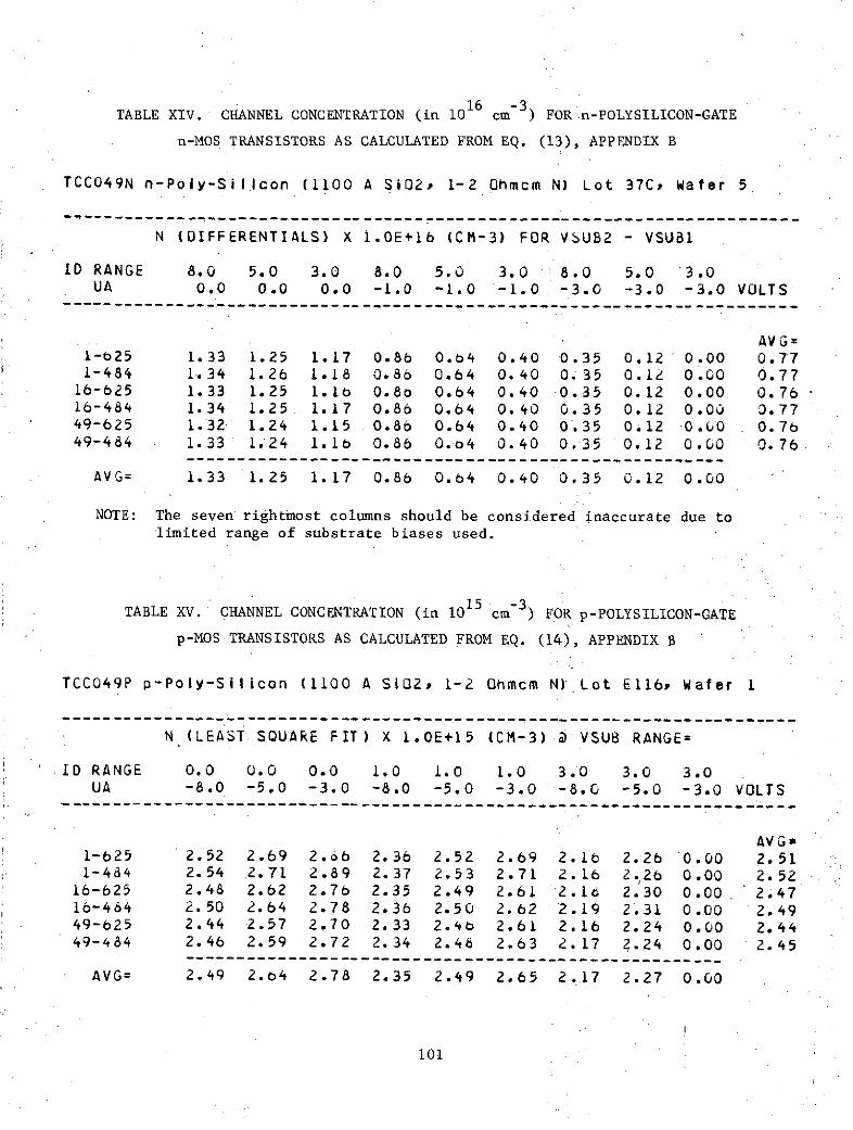
TABLE XIV. CHANNEL CONCENTRATION (in 10 cm ) FORn-POLYSILICON-GATE
n-MOS TRANSISTORS AS CALCULATED FROM EQ. (13), APPENDIX B
TCCO49N n-Poly-Silicon (1100 A SiOZ, 1-2 Ohmcm N) Lot 37C, Wafer 5
- -----------------------------------
N (DIFFERENTIALS) X 1.OE+16 (CM-3) FOR VSUB2 - VSUB1
ID RANGE 8.0 5.0 3.0 8.0 5.0 3.0 8.0 5.0 3.0UA 0.0 0.0 0.0 -1.0 -1.0 -1.0 -3.0 -3.0 -3.0 VOLTS
--------------------------------------------------------------
AVG=1-b25 1.33 1.25 1.17 0.86 0.b4 0.40 0.35 0.12 0.00 0.771-484 1.34 1.26 1.18 0.86 0.64 0.40 0.35 0.12 0.00 0.77
16-625 1.33 1.25 1.16 0.80 0.64 0.40 0.35 0.12 0.00 0.7616-484 1.34 1.25 1.17 0.86 0.64 0.40 0.35 0.12 0.00 0.7749-625 1.32 1.24 1.15 0.86 0.64 0.40 0.35 0.12 0.00 0.7b49-484 1.33 1.24 1.16 0.86 0.04 0.40 0.35 0.12 0.00 0.76
AVG= 1.33 1.25 1.17 0.86 0.64 0.40 0.35 0.12 0.00
NOTE: The seven rightmost columns should be considered inaccurate due tolimited range of substrate biases used.
15 -3TABLE XV. CHANNEL CONCENTRATION (in 10 cm ) FOR p-POLYSILICON-GATE
p-MOS TRANSISTORS AS CALCULATED FROM EQ. (14), APPENDIX B
TCC049P p-Poly-Silicon (1100 A Si02, 1-2 Ohmcm N) Lot E116, Wafer I
------------------------------------------------------------------------------
N (LEAST SQUARE FIT) X 1.OE+15 (CM-3) @ VSUB RANGE=
10 RANGE 0.0 0.0 0.0 1.0 1.0 1.0 3.0 3.0 3.0UA -8.0 -5.0 -3.0 -8.0 -5.0 -3.0 -8.0 -5.0 -3.0 VOLTS------------------------------------------------------------------------
AVG=1-625 2.52 2.69 2.66 2.36 2.52 2.69 2.1b 2.26 '0.00 2.511-484 2.54 2.71 2.89 2.37 2.53 2.71 2.16 2.26 0.00 2.52
16-625 2.48 2.62 2.76 2.35 2.49 2.61 2.18 2.30 0.00 2.4710-464 2.50 2.64 2.78 2.36 2.50 2.62 2.19 2.31 0.00 2.4949-625 2.44 2.57 2.70 2.33 2.4b 2.61 2.16 2.24 0.00 2.4449-484 2.46 2.59 2.72 2.34 2.48 2.63 2.17 2.24 0.00 2.45
- ---------------------------------------------------
AVG= 2.49 2.64 2.78 2.35 2.49 2.65 2.17 2.27 0.00
101

TABLE XVI. n-SUBSTRATE RESISTIVITY AS CALCULATED FROM TABLE XV
TCC049P p-Poly-Silicon (1100 A Si02s 1-2 Ohmcm N) Lot El16, Wafer 1
RHO X 1.OE+00 (OHMCM) N-TYPE @ VSUB RANGE=
ID RANGE 0.0 0.0 0.0 1.0 1.0 1.0 3.0 3.0 3.0UA -8.0 -5.0 -3.0 -8.0 -5.0 -3.0 -8.0 -5.0 -3.0 VOLTS
AVG=1-b25 1.84 1.73 1.63 1.96 1.84 1.73 2.14 2.04 0.00 1.861-484 1.83 1.72 1.62 1.95 1.84 1.72 2.13 2.04 0.00 1.8616-625 1.87 1.77 1.69 1.97 1.87 1.78 2.12 2.01 0.00 1.8916-484 1.86 1.76 1.68 1.96 1.86 1.77 2.11 2.00 0.00 1.8849-625 1.90 1.81 1.72 1.99 1.88 1.78 2.14 2.06 0.00 1.9149-484 1.89 1.80 1.71 1.98 1.87 1.77 2.13 2.06 0.00 1.90
AVG= 1.86 1.7o 1.67 1.97 1.86 1.76 2.13 2.04 0.00
NOTE: The nominal value of the silicon used is 1 to 2 ohms-cm
102

TABLE XVII. n-MOS TEST RESULTS OF PAST PROCESSED LOTS
Field-OxideP Of Transistor Gate-Oxide Transistor
TCC-049 Interconnect s nwellWell V N For VTO K I-R N For From Sub.Lot No. Metal TFO sa TO ss(/CO) (Volts) Field Oxide (Volts) (PPM) Gate Oxide Bias
1 Aluminum 1035 12.5 1.7 x 10¹¹ 0.97 190 870 9 x 10¹⁰ 2.1 x 10¹⁶
2 Aluminum 990 0.84 199 -
3 Al + B..L. 1100 - -2.4 78 -
4 Aluminum 1140 8.5 3 x 10¹¹ -2.1 80 51 3 x 10¹¹ 1.5 x 10¹⁶
4E Aluminum 1140 11.2 3.5 x 10¹⁰ 2.13 83 630 2 x 10¹⁶
285 Aluminum 994 3.3 3.4 x 10¹¹ 0.51 39 54 2.3 x 10¹¹ 1.3 x 10¹⁶
2E Al + B.L. 1280 17 2.89 45 398 2 x 10¹⁰ 2.5 x 10¹⁶
303 Al + B.L. 824 18.2 5.4 x 10 1.15 68 164 1.2 x 10¹¹ 1.2 x 10¹⁶
E-8 Beam Lead 14.6 0 0.88 89 110 7 x 10¹⁰ 7.2 x 10¹⁵
E-14 Beam Lead 18.3 "*-9 x 10 1.17 80 92 6 x 10 9.5 x 10¹⁵
10 Beam Lead 11.2 8 x 10 1.16 85 262 8.7 x 10¹⁰ 1.1 x 10¹⁶
10 11 16E-21 Beam Lead 15.8 7 x 10 1.1 64 37 1.3 x 10 1.3 x 10
10 10 1631 BeamLead 17.4 1x10 1.5 91 68 2x10 1.1 x 10E-26A Beam Lead 12.4 6 x 10¹⁰ 0.82 59 15 1 x 10¹¹ 8.7 x 10
" Depletion mode n-MOS transistors due to high surface-state density.
Negative N indicates inaccuracy in the nWELL
tCorrected TCC049 Mask.
103

TABLE XVIII. p-MOS TEST RESULTS OF PAST PROCESSED LOTS
Field-OxideField-Oxide Gate-Oxide Transistor -p Transistor Psub.
TTC-049 InterconnectLot No. Meta Ineronnect Substrate VTF O N For VTO K I-R N For From Sub
(Qcm) (Volts) Field Oxide (Volts) (PPM) Gate Oxide Bias
1 Aluminum 1 to 2 -13 1.3 x 10 -1.03 60 880 8 x 10 -
2 Aluminum 1 to 2 - -0.61 35 -
3* Al + B.L. 1 to 2 - - -2.3 28 598 3.2 x 10¹¹
4* Aluminum 1 to 2 -23.6 3.5 x 10¹¹ -2.4 23 490 3 x 10¹¹
4E Aluminum 1 to 2 -12.3 3.3 x 10 -0.96 68 166 5.6 x 10¹⁰
285* Aluminum 1 to 2 - -1.97 55 324 1.1 x 10 5 Qcm
10 102E Al + B.L. I to 2 -15.2 3.5 x 10 -0.87 32 206 5.4 x 10 2.4 Qcm
303 Al + B.L. 1 to 2 -21.3 2 x 10 -1.45 33 420 1.4 x 10¹¹ 2.1 Qcm
11 10E-8 Beam Lead 1 to.2 -14.7 1.6 x 101- -1.42 34 182 1.2 x 10 1.7
E-14 Beam Lead 1 to 2 -34.7 6 x 10 -1.49 30 93 1.3 x 10 1.6
10, Beam Lead 1 to 2 -12.2 1.4 x 10¹¹ -0.96 33 350 8 x 10 2.5
E-21 Beam Lead 1 to 2 -14.4 1.2 x 10¹¹ -1.2 30 74 1.3 x 10¹¹ 2.3
31 Beam Lead 1 to 2 -20.3 2.4 x 10 -1.4 23 619 1.6 x 10 2.7
E-26At Beam Lead 1 to 2 -22.5 2.6 x 10 -1.35 24 127 1.4 x 10 2.3
High-threshold p-MOS transistors - due to high surface-state density.Corrected TCC-049 mask.
104

TABLE XIX. TYPICAL n-MOS TEST TRANSISTOR PARAMETERS - RECENTLY PROCESSED LOTS
Field-OxideP (/) Transistor Gate-Oxide Transistor
TCC-049A ALU Ps (11/0) Transistor nWELLChip of n N For VT BVSD K I-R I (mA) N For From Sub.Yield Doped Oxide ss TO D ss
(Volts) Field Oxide (Volts) (Volts) (PPM) V = V = IOV Gate Oxide Bias
35A 2 24 1.1 18 60 46 4.2 1.2 x 10¹¹ 1.4 x 10¹⁶
35B 17 150 8.9 3 x 10¹¹ 1.7 18 63 56 3.5 1.1 x 10¹¹ 2.3 x 10¹⁶
37B 53t 18 14.2 4.5 x 10¹⁰ 1.2 21 85 31 4.8 6.3 x 10¹⁰ 1.2 x 10¹⁶
37C 32t 31 12.8 1.2 x 10¹¹ 1.4 20 79 55 4.5 6.0 x 10 1.4 x 10¹⁶
E-105 2 25 10.3 1.5 x 10¹¹ 0.86 20 59 45 4.1 1.5 x 10¹¹ 1.3 x 10¹⁶
38C 15t 77 9.5 1.8 x 10¹¹ 0.94 20 61 174 4.0 1.6 x 10¹¹ 1.4 x 10¹⁶
39C 32 45 13.3 3 x 101 2.6 18 51 200 2.6 2 x 10¹⁰ 3.0 x 10¹⁶
t6-volt operation only.

TABLE XX. TYPICAL p-MOS TEST TRANSISTOR PARAMETERS - RECENTLY PROCESSED LOTS
Field-Oxide Gate-Oxide TransistorP (Q/) Transistor sub
TCC-049A ALU s V N For V BV K I-R I (mA) N For From Sub.
LT . Chip of p+ TFO ss TO D ss BiasLot No. Yield Doped Oxide (Volts) Field Oxide (Volts) (Volts) (PPM) VDS = VGS = 10V Gate Oxide
35A 2 23 -1.03 -23 35 132 -3.5 7.7 x 10 1.6
35B 17 18 -1.3 -24 19 117 -2.2 1.1 x 10 1.3
10 1037B 53t 24 -10.8 6 x 10 -0.96 -25 34 126 -2.4 7.6 x 10 1.5
37C 32t
17 -0.65 -23 36 205 -2.5 5 x 10 1.6
E-105 2 20 -14.9 1.1 x 10 -1.6 -22 24 70 -1.9 1.7 x 10 1.3
38C 15 25 -22.7 3 x 10¹¹ -1.3 -23 32 185 -2.0 2 x 11 3
10 1039C 32 35 -8.9 6 x 10 -0.7 -25 35 250 -2.3 7 x 10¹⁰ 3
t6-volt operation only.

The problems associated with these omissions are discussed elsewhere. The
maximum wafer yield was about 30 percent, but the average yield is much less
than this. Also, comparison of columns two and three of Table XIX indicate
that 10-volt yield is only appreciable when the n+ doped-oxide resistivity ex-ceeds 45 ohms/O. These facts indicate that the masks are still not optimum for
high yield. Two problems remain. The first is mask runout, which makes for a
large variation in yield between wafers of the same lot. Also, n+-p+ break-
downs of 6 volts indicate that a violation still exists in the distance betweendiffused areas of different doping types. A look at the.large variation insupply leakage (IL for VDD = 10 volts) over a single wafer - from 1 microampere
to 10 milliamperes - confirms that there is not enough margin between the pro-cess and the masks (see Figure 69). We have demonstrated, however, that byincreasing the. n+ source-drain resistivity, the existing mask set can be usedto produce 10-volt devices with resonable yield. But this is accomplished atthe cost of a reduction in n-MOS current output and, hence, speed.
D. TEST-CIRCUIT PERFORMANCE
.1. MOS ARRAY FUNCTIONAL TESTING
The MOS-array tester used is a rack-mounted test generator consisting ofthree separate panel-mounted units. The first unit is a 40-word by 100-bit
word generator, the second unit is a clock generator, and the third unit:is awork area. The word generator is capable of 40 separate outputs, each with aseparately adjustable zero and one level. Each word is programmed by diodepins in matrix boards situated on the front of the generator. Each diode pincauses a transition from ground to -V level or vice versa. The clock generatorwas not used. The work area has four built-in power supplies and a 40-pinarray socket which is connected to the appropriate probe card. Functionaltesting is done on an MOS-array tester. A functional-test pattern is generatedand applied to the array under test (a) at wafer sort, using a face-up probecard; (b) after back etch and separation, using a face-down probe card; and(c) after packaging, prior to shipping. In addition to supplying the testinputs to the array, the pattern contains the expected outputs from the arrayfor comparison with the actual array outputs. The test pattern exercises allthe inputs to every gate in the array to assure that each input performs cor-rectly. Comparison was made on a Hewlett-Packard 547 oscilloscope.
107

W5 LOT 35A
25 -
20 -
o=
015O cc010
z 10 -
10 1(2 103 104
LEAKAGE AT 6 VOLTS (MICROAMPERES)06668L
Figure 69. Typical Leakage Distribution on Wafer - All Chips

2. PROPAGATION-DELAY AND PAIR-DELAY MEASUREMENTS ON NOR CHAINS
The five-stage NOR gate (silicon gate) test circuit shown in Table XXI
consists of five 1120's and one 1520. The results of the propagation-delay
measurements made with this circuit are given in Table XXI. Note that the
average delay at 10 volts is 11 nanoseconds, as opposed to about 14 nanoseconds
for the aluminum-gate design. About 2 to 3 nanoseconds of this 11-nanosecond
total came from the polysilicon interconnect resistance, which is absent in the
aluminum-gate circuit. The polysilicon gate length (as defined by the mask)
was 0.25 mil on all devices. Table XXII shows the NOR gate pair-delay test
circuit and the results of the measurements made with it. The delay per stage
is about 12.5 nanoseconds due to the added complexity of this circuit.
Table XXIII shows several silicon-gate test transistor parameters for lots
processed previously. Included at the bottom is some data for equivalent
aluminum-gate devices. The most important performance parameter is the drain-
current output, which is a strong function of effective channel length as
shown. The only speed data taken were measured on lot E-8. A comparison of
the drain-current output for each lot listed shows that lots 2 and 10 would
have given much shorter delays. The higher drain currents of these lots were
obtained at the expense of breakdown voltage and, to a smaller extent, overlap
capacitance. These considerations are at variance with more recent yield data.
n-MOS current output had to be depressed in order to obtain appreciable yield
at 10 volts with the masks in hand (see Table XIX), and so slower than optimum
speeds are to be expected from most, but not all of these lots. In the next
paragraph, the factors affecting yield will be detailed.
E. YIELD ANALYSIS
When early wafer lots were processed with aluminum to reduce processing
time, it was found that the most complicated circuits were not operational due
to metal discontinuity. In some cases the polysilicon lines were marginal
where they crossed the stepped (field) oxide (see Figures 70 and 71). A
sloped stepped-oxide process, developed at RCA, was introduced to solve this
problem. Scanning electron microscope pictures of our improved process (Fig-
ures 72 through 74) show the excellent polysilicon and beam-lead continuity
now being achieved.
109

TABLE XXI. PERFORMANCE OF THE NOR GATE WITH PAIR DELAY
1520
1520 11520 1520 1520
8pF 21 22 8pF
TCC-049 Delay Delay Delay Delay Pair Delay Pair DelayChip No. 18 21 18 21 18 19 18 19 21 22 21 22
II II II IF I II I IE8-10 31 32 70 67 23 24
E8-11 34 37 76 74 26 26
E8-14 33 35 74 72 25 25
E8-18 33 36 78 75 26 27
Notes: 1. All delay times are in nanoseconds.2. The estimated delay for the 1520 output buffer is
approximately = 10 nanoseconds.

TABLE XXII. PERFORMANCE OF THE FIVE-STAGE NOR GATE WITH PROPAGATION DELAY
1520
INPUT OUTPUT
TCC-049 10 Volts 12 Volts 15 Volts Output
Chip No. Delay Delay Delay Delay Delay Delay Capacitance
11 10 11 10 11 10 11 10 11 10 11 10 Pin 10
f 1 _F11 I _L (pF)
E8-3 66 56 57 53 56 50 7.7
E8-4 70 63 58 55 43 50 8.0
E8-5 69 61 58 54 57 53 7.8
E8-6 70 62 58 56 57 51 7.7
V - VDD = 0 V V - V = 12 V VS - VDD = 15 V
I Avg. = 69 ns I Avg. = 58 ns Avg. = 53 ns
L Avg. = 60.5 ns L Avg. 54.5 ns _ Avg. = 51 ns
Avg. Per Stage Avg. Per Stage Avg. Per Stage
= 11 ns 9.5 ns = 8.6 ns
Notes: 1. All delay times are in nanoseconds.
2. The propagation delay for the equivalent aluminum-gatecircuit = 80 nanoseconds or 14 nanoseconds per stage.

TABLE XXIII. TEST TRANSISTOR DATA SHOWING THE PROCESS PARAMETERS THAT AFFECT SPEED
TCC-049 n-MOS p-MOS
Lot No. BVSD ID BVSD ID
VGS = VDS VGS = VDS= 10 V gm K Leff. = 10 V gm K Leff. Lgeo.
(V) (mA) (Ga) (V) (mA) (~U) (mil)
E-8 19 4.2 800 89 0.16 -26 2 320 34 -0.16 0.24
E-14 22 3.6 800 78 -0.15 -27 2.4 300 30 -0.18 0.23
E-21 22 3.5 650 49 -0.19 -27 1.6 300 24 -0.19 0.27
10 20 5.3 820 85 -0.13 -28 3.1 370 33 -0.13 0.21
2 13 9.0 1100 258 -0.09 -14 6 81 -0.09 0.19
Aluminum-Gate 21 3.6 -700 - - -35 1.4 -270 - -0.20 0.3Equivalent
Notes: 1. L = L - 2X. is an estimate of actual channel length.eff geo j
2. The junction depth is 0.03 < X. < 0.05 mil.

POLYSI LICONGATE INTACT
06367V
Figure 70. Tapered Stepped Oxide
POLYSILICONGATE BROKEN
AT STEP
06368V
Figure 71. Standard Stepped OxideThis page is reproduced at theback of the report by a differentreproduction method to provide
113 better detail.

5000X 06369VFigure 72. SEM Detail of Beam-Lead Metal Crossing Over Polysilicon
114

800X 06370VFigure 73. SEM of a Portion of ALU Chip Showing Beam-Lead
Interconnect Metal Crossing Polysilicon Lines.
06371V
Figure 74. SEM Detail Showing Beam-Lead Metal-to-Polysilicon Contact.
115

But several other problems kept the actual device yield of TCC-049 very
low. Two major and several minor problem areas were identified. The first
major problem was the result of the sloped-oxide etch that increases the hole
in the thick oxide. Light emitting n+p+ junctions in the n+ drain regions
were observed. This indicated that the stepped-oxide edge had shifted so much
from its original position (due to sloping) that both types of doped oxide (p+
and n+) were falling within a drain area, see Figure 75. This was rectified
by tighter control of the sloped-oxide etch and by making the mask for the oxide
hole 0.1 mil smaller all around. It had manifested itself electrically by low
breakdown of the n- MOS transistor. The second major problem was found in one
particular cell. There, the ground strap contact between the p+ guard band and
the n+ source was not fully covered with a deep well diffusion. Since the p+
guard band and the n+ source diffusion have roughly the same depth, process
variations did or did not allow a short between the n+ source and the n sub-
strate, see Figure 76. Latest leakage currents are now in the microampere
range as opposed to several hundred milliamperes on early lots.
Theoretical analysis indicates that only a 4.5-micron side-way diffusion
is to be expected for an 8-micron deep well. At the corners of the oxide mask,
only 2.5 microns are to be expected. The n-substrate areas between the well
diffusions and the p+ guard band were observed, especially around the corners.
This increased the well leakage somewhat, but not catastrophically. A design
rule change to increase the well mask by 0.1 mil was made.
A similar well-mask problem was caused by the library cell boundary con-
ditions. The notches in the p-well areas, see Figure 77, allow cut-off of the
n-MOS transistor even for somewhat "dirty" field oxide. For clean oxides they
are not necessary and do increase the well perimeter and increase the p-well
leakage to the n-substrate, however, not catastrophically.
Mask changes of the TCC-049 were made to correct all of the problems listed
above.
F. LIFE TESTING
Beam-lead chips from various lots were packages in 24-lead DIC packages
for life testing. The wiring of the life-test board is shown in Figure 78.
116

UNDERCUT n+ GLASS6 TH. MASK
p+ GLASS \\\\\\\\ GATEOXIDE
SUBSTRATE
P+ p- WELL
P+ GUARD BAND
06525 L
Figure 75. n - p Diode Resulting from Enlarged Stepped-Oxide Mask and Undercut Doped-Oxide Mask
117

n SUBSTRATE /////////// n+
p- WELLp* GUARD BAND SHORT
n+ SHORTTHRU p GUARD BANDn SUBSTRATE
06526L
Figure 76. n+ Source Diffusion Shorting out p+ Guard Band
118

06514V
Figure 77. TCC-049 Level-One Mask (Well)
This page is reproduced at theback of the report by a different
reproduction method to providebetter detail.
119

VDD
3
24
23
GATE-OXIDE FIELD-OXIDE
5 TRANSISTORS TRANSISTORS
VSSOR
VDD 14
13
6 7
15VS
VDD= 10VVSS= 0 V
ALL RESISTORS 47 KOHMS06485L
Figure 78. Bias Life-Test Circuit for TCC-049A Test Transistors
120

The two complementary-gate-oxide transistors are connected in the inverter
mode. The common-gate connection (pin 8) is connected to VDD for half the
devices under test and to VSS for the other half. Thus, the p-MOS devices
are on in half the samples and the n-MOS devices are on the other half. The
field-oxide devices are connected as capacitors during test to simulate the
situation on the actual chip. Changes in the thresholds of these devices give
us a measure of the amount of ion drift in the field oxide.
1. OPERATING LIFE-TEST DATA
Twelve units from lot E-14 were placed on life test at 125 C. The p-MOS
and n-MOS thresholds, measured after intervals of 168 hours, 336 hours, and
500 hours on four typical units, are shown in Figure 79. The maximum shift on
the n-MOS gates (n+ doped polysilicon) is of the order of 12 percent. For the
p-MOS gates (p+ doped polysilicon), however, the shift after 500 hours under
life is over 300 percent in the direction of increasing thresholds. This in-
stability is now believed to originate from small amounts of impurities in the
silane of the boron-doped oxides. In the case of the phosphorus-doped oxides,
they are gettered out during the annealing cycle. Consequently, heavier levels
of boron would make for less contaminants in the boron-doped silane. This has
been ovserved. Recently, units from lot 37C were put on life test. The results
appear more promising than the data for lot E-14. The boron-doping level was
increased to about 18 ohms/o (measured on the substrate) to improve stability.
2. TEMPERATURE BIAS STRESS
In order to better characterize the stability of the process, C-V plots
were taken on several processed lots after stressing at 300 C for 1 minute at
a positive bias of 12 volts. The results, shown superimposed in Figures 80
through 83, confirm the life-test findings of almost zero shift on the n+ doped
polysilicon gates and some negative shift on the p+ doped gates. Lot 2E ob-
viously had heavy ionic contamination of the gate oxide, since both p+ and n+
doped gates show large shifts. Lot E-105, which had lighter boron doping,
shows a 6-volt shift on p+ gates, but only a 0.2-volt shift on n+ doped gates.
This result is typical of contamination by light boron-doped polysilicon gates.
Table XXIV shows the shifts in the minimum of the C-V curves.after 1 minute at
3000C under +12 volts.
121

LOT E-14
3
1-
0-
-4
-3 -
-2
-1
150 300 450
HOURS UNDER LIFE06515L
Figure 79. Initial Life Data from TCC-049A Test Transistors
122

LOT E-14 BL
C/Co
LOT 31 BL
---- INITIAL
300 0C +12 V;1 MIN
BL= BEAM LEAD
-8 -6 -4 -2 VOLTS 2 4 6 8
06516L
Figure 80. CVBT Curves of p+ Doped Polysilicon p-MOS Test Transistor Gates

LOT E-14 BL f j
C/Co
LOT 31
- INITIAL
300oC, 12 V; 1 MIN
BL= BEAM LEAD
I I I I I I I I-8 -6 -4 -2 2 4 6 8
VOLTS
06517L
Figure 81. CVBT Curves of n+ Doped Polysilicon n-MOS Test Transistor Gates

35A W-5 p-MOS
37B p-MOS
LOT E-105
INITIAL
---- 3000C+12 V 1 MIN
I I I I-4 -2 2 4
VOLTS 06669L
Figure 82. CVBT Curves of p+ Doped Polysilicon p-MOS Test Transistor Gates

LOT 34B
LOT E-105
LOT 37 n-MOS
- INITIAL
3000C +12 V 1 MIN
-4 -2 2 4
VOLTS06670L
Figure 83. CVBT Curves of n+ Doped Polysilicon n-MOS Test Transistor Gates

TABLE XXIV. TEMPERATURE BIAS STRESS DATA
Lot AVTN AVTP BoronNo. @ +10V, 3000 C @ +10V, 3000 C Doping
(Volts) (Volts) Level
10 0.1 0.6 Heavy
*2E 10 >10 Light
E-14 0.05 1 Light
31 0 0.2 Heavy
E-105 0.3 6V Light
35A - 0.3 Heavy
37B 0.05 0.2 Heavy
34B 0 0 Heavy
*Contaminated gate oxide.
127

G. DELIVERED SAMPLES
On 21 December 1973, 16 samples of the ALU chip were delivered to the con-
tracting agency. The test-transistor data on the chips supplied are shown in
Table XXV. One unit was packaged in an 80-lead universal beam-lead package as
shown in Figure 84. Drawings of the pin-out data were also supplied as shown
in Figure 85.
128

TABLE XXV. TEST-TRANSISTOR DATA OF DELIVERED TCC-049A SAMPLES FROM LOT 39C
Gate-Oxide Transistors Field-OxideTransistors
K- I D @
V BV Factor V = 10V N N V NSTO SD SG ss pwell Pn-substr VTFO ss
VSD = 10V
(V) (V) (yA/V 2 ) (mA) (cm-2 ) (cm- 3 ) (Ohm-cm) (V) (cm- 2 )
n-MOS 2.6 18 51 2.6 2 x 101 0 3.0 x 10- 13.3 3 x 10
p-MOS -0.69 -25 35 -2.3 7 x 10¹⁰ 3.0 -8.9 6 x 10¹⁰

06671 V
Figure 84. Packaged TCC-049A Chip
This page is reproduced at theback of the report by a different
reproduction method to provide
better detail.
130

80 75 70 65 60 55 50 45 41
TCC-049A
10 15 20 25 30 35 40.025 TYP.025 TYP
TERM. NO. 11.980
CHIP TO SUBSTRATE INTERCONNECTION
BEAM SUBSTRATE BEAM SUBSTRATE BEAM SUBSTRATE: UNCTIOON FUNCTION FUNCTION
NO. TERMINAL NO. TERMINAL NO; TERMINAL
1 9 MOST POS. VOLT 16 34 SPM (N + 1) 31 65 CTR (N)
2 12 CL2 17 35 101 32 66 OFLO
3 13 CLI 18 36 SPM (N) 33 67 C(N)
4 14 127 19 45 SLCl 34 68 20
5 15 SM (N + 1) 20 46 SLC2 35 69 122 GRD
6 16 126 21 47 SPM (N - 11 36 70 123
7 25 SM (N) 22 48 OPA-N 37 71 124
8 26 SLC3 23 49 MOST NEG GRD 38 72 128
9 27 104 24 52 CL4 39 73 129
10 28 SPM (N + 3) 25 53 OPA (N + 1) 40 74 C (N +4)
11 29 SPM (N + 2) 26 54 SM (N 3) 41 75 OPATN+3)
12 30 132 27 55 120 42 5 130
13 31 125 28 56 SM (N+2) 43 6 CTR (N+4)
14 32 103 29 57 121 44 7 OPA(N
15 33 102 30 64 131 45 8 C (N+8)
06672L
Figure 85. Pin-Out Data for the TCC-049A Chip
131

SECTION IV
CONCLUSIONS
A self-aligned silicon-gate beam-lead process for COS/MOS devices has been
developed using deposited doped oxides as diffusion sources. The test vehicle,
a four-bit adder, was designed from library cells interconnected by metal and
polysilicon to form the desired circuit. These cells have been confirmed as
correct, and a library of simple silicon-gate circuits is now in existence
together with a set of design rules compatible with the process.
The fabrication process involves a metallization scheme of evaporated Pd-Ti
layers instead of the sputtered Pt-Ti system which may cause threshold shifts.
Although further refinement is necessary to maintain high yields at low supply
leakage, several problems including metal over polysilicon continuity, metal
over stepped-oxide continuity, and stability of boron-doped polysilicon gates
have been solved. The question of speed has not been fully answered. Because
of the integrated-cell library approach, speed depends appreciably on the re-
sistance associated with the polysilicon interconnects. These cannot be reduced
below 18 ohms/square. However, the low thresholds and relatively high current
output per mil of device width make for a faster circuit.
The two-layer metallization scheme developed on this program has resulted
in a 40-percent reduction in chip size compared to the aluminum-gate equivalent.
133

APPENDIX A
THEORETICAL DISCUSSION OF THE METAL-OXIDE-SILICON SYSTEM
1. ENERGY-BAND STRUCTURE
An important feature of the metal-oxide-silicon (MOS) system is its effect
upon the threshold voltage. The Si-SiO2 -Si system can be viewed as a metal-
silicon dioxide-silicon system whose metal has been replaced by silicon. Ac-
cordingly, a change in the work function difference would be expected because
of the dissimilarities between the metal and the silicon.
The energy-band diagram of the general metal-insulator-semiconductor is
shown in Figure A-1 (1' 2 ) The semiconductor is p-type .and the gate voltage is
zero in this MIS system. The surface states and the oxide charges are assumed
to be zero.
The work function of a material represents the energy required to move an
electron from the Fermi level, in a given material, to a given reference level.
In a system at equilibrium, i.e., no net transfer of energy, the Fermi level
of the metal and the semiconductor must be level or constant throughout the
energy band.
According to convention, the potentials are considered positive in the
negative R direction. In addition, energy is expressed in electron volts and
I. S.M. Sze, Physics of Semiconductor Devices, Wiley-Interscience, 1969.
2. A.S. Grove, Physics and Technology of Semiconductor Series, Wiley, New York,1967.
-IG PA( NK NOT F 135P r" *~~U"lFI~~

VRv i
I-1
VG 0XNss 0
Xs
qM SSPEG
2
.i--EC
EF EF
METAL GATE p -TYPE SEMICONDUCTOR
INSULATOR05813L
Figure A-i. Energy Band Diagram for the Metal Gate-Insulator - p-Type Semiconductor Substrate
136

potential in volts. Let R* be the reference level of a free electron, then the
potentials from the Fermi level to line R for the metal and that of the semi-
conductor can be equated as
EGV. + X. + 4m = X +- - + + 4.(1)1 1 m s 2 s F SP
By definition
MS M S.*-. S ....... ................ (2)
or, for a p-type semiconductor substrate
MSp M - s..... (3)SP SP
then, 4MSSP can be represented as
EG
Mi + (x + F S P ) = - (Vi + ) .. . . . . . . (4)MP SP i S
Replacing the metal gate in Figure A-I with an n-type semiconductor gate,we have represented in Figure A-2 the energy-band diagram of an n-type semi-
conductor gate-insulator-p-type-semiconductor substrate. If we assume that
the band-gap theory is still applicable, we have, similar to Eq. (1)
E E
i s s 2 F + . . . . . .. . . .... (5)S + G N SP
By definition
GN SP GN SP
then, by Eq. (5), (6), and Figure A-2 (cancelling like terms and rearrange-
ment) we have
*See Notation.
137

Rvi
VG 0
XS NSS : 0
SGN Xs SSP
EG2
EG EC
EC -- -- EEF
Ei -- ---- - ------ EVIPGNEv
n-TYPE SEMICONDUCTOR P-TYPE SEMICONDUCTORGATE
SUBSTRATE
INSULATOR
05814LFigure A-2. Energy Band Diagram for the n-Type Semiconductor Gate-Insulator - p-Type Semiconductor Substrate
138

SGNSSP IFG N FFsP = (V i ..S) . .............. (7)
or
SGNSsp (F GN+ +FSP) (8)
For the case where the silicon gate is p-type and the silicon substrate is
also p-type we find, utilizing the procedure outlined above, that
SGPSSP FGP FSP
Three conditions may exist:
a. The doping level of the gate is greater than that of the substrate
since
'FGP F ... ...... . . . . . . ..... .. . . . . . . .. (10)
then,
SGp SS FGp F > 0 . . . . . . . . . . . . . . . . . .(11)
b. The doping level of the gate is equal to that of the substrate since
F F .... . . . ........... ... . . . ... . .. . (12)GP SP
then,
SGpSsP qFGP .FSP = 0. . . . . . . . . . . . (13)
c. The doping level of the gate is less than that of the substrate
since
\F < \/F ......... ......................... (14)GP SP
then,
SS FG < 0 . . . . . . . . .. . ........ (15)GPSP GP1 SP
139

Replacing the metal gate in Figure A-3 with a p-type semiconductor gate,we have, as represented in Figure A-4, similar to Eq. (5)
EG EX +-+ = V +x +-++ - (16)s 2 F S 2 S ......... (16)
By definition
SGpS N FGP (Vi + 41S ) ............... (17)
or
S F F .... .................... (18)SGPSSN FGP FSN
For the case where the silicon gate is n-type and the silicon substrate
is also n-type, we find, utilizing the procedure outlined above, that
SGNSN = FGN FSN ............... ........ (19)
Three conditions can then exist:
a. The doping level of the gate is greater than that of the substrate
since
FGN > FSN . ............... .......... (20)
then,
GNSsN FGN +S N < 0 . . ..... . . . . . . . . . . . . (21)SNS SN F GN F SN
b. The doping level of the gate is equal to that of the substrate
since
'FGN Fs N (22)
then,
S NSSN = 0 . . . . .. . . . . . ........................ . (23)
c. The doping level of the gate is less than that of the substrate
since
140

- R
vi
Xi
VG =0
NSS :
nm Xs
EG2
EC
EF EF
..-.- _- i
S EV
METAL GATE n-TYPE SEMICONDUCTORSUBSTRATE
INSULATOR
05815L
Figure A-3. Energy Band Diagram for the Metal Gate-Insulator - n-Type Semiconductor Substrate
141

R
VG :0
OSGP XS NSS: 0
#XS
ESSN
EC
EG pE
EF I _" --- EF
EV
p-TYPE SEMICONDUCTOR n-TYPE SEMICONDUCTORGATE SU BSTRATE
INSULATOR05816L
Figure A-4. Energy Band Diagram for the p-Type Semiconductor Gate-Insulator - n-Type Semiconductor Substrate
142

'FG N F ......... . . . . . . . . (24)
then,
SGNSN FGN SN .......... (25)
2. THRESHOLD VOLTAGE
In paragraph 1, the work function were derived for the four possible con-
ditions of gate and substrate doping types. If we assume that the energy-
band theory continues to apply for a silicon-gate structure, then the thres-
hold voltage at ID = 0 can be defined as(2)
t tVT SS r4q S N 4S qrF S - qNS Ox-. . . . . . . . . (26)S ox
fox
where #SS' depending on the conditions, is described by Eq. (8, 9, 18, or 19)
and F', the generalized FGP, FGN' FSP ' IFSN
by
KT N + N.
In N. ' . ' ' ...... .. .... . ...... . . (27)
and, if VG = 0,
2KT N + N.
S= n ± 2 4 F... ... . .... ......... . . (28)
Because the silicon-gate layer can serve as an additional interconnection
plane, its resistance is made as low as possible. If we assume that the im-purity concentration of either the p- or n-doped silicon gates is greater
19than 3 X 10 , the Fermi potential would then be greater than half the band
gap of silicon, i.e., 0.55 eV. In this case, FGN or F would be equal to0.55 eV. GN FGP
143

Let us consider four combinations of silicon gate-silicon dioxide-silicon
structure and assume the following for all cases:
substrate orientation <100>
oxide charge = 0
V = 0 and S = 2+'G S F
t = 0.10 micrometerox
10 -2NSS = 5.00 x 10 cm
-13ox = 3.40 x 10 F/cm
-12Si= 1.04 x 10 F/cm
T = 298.10 K
q = 1.60 x 10- 1 9 coulombs
4F = \F = 0.55 eVGN GP
CASE I: AN N-TYPE SILICON GATE AND A P-TYPE SUBSTRATE
Given:
16 -3NS = 1.00 x 10 cm
19 -3NGN = 3.00 x 10 cm
From Eq. (27)
F = 0.35
from Eq. (8)
SGNSSP FGN SP ) = -0.20
and Eq. (26) for VT
t t
V S + O 4q ES NS F + 2 IF - qNxssSGNSSP ox Fox
VTN N 1.00 volt
144

CASE 2: A P-TYPE SILICON GATE AND A P-TYPE SUBSTRATE
15 -3N = 6 .80 x 10 15 cm
14 -3NGP 3.00 x 10 cm
Substituting the given values in Eq. (11) and the results and the assumed
values in Eq. (26), we get
V = 2.00 voltsNP
Comparing the results of Case 1 and Case 2, note that by changing the gate
type from n to p, the threshold voltage is increased by 1 volt.
CASE 3: A P-TYPE SILICON GATE AND AN N-TYPE SUBSTRATE
15 -3NSN = 5.00 x 10 (cm )
19 (cm-3N = 3.00 x 10 (cm )
From Eq. (27)
F N = 0.33SN
from Eq. (18)
SGPSSN = 0.88
and Eq. (26) for VT
t tV = ox S S4-q eS NS - 211F N ssT pp S GPS SSF F ss
PP PN ox
V = - 1.01 volts
CASE 4: AN N-TYPE SILICON GATE AND AN N-TYPE SUBSTRATE
15 -3N = 2.50 x 10 (cm )
19 -3NGN = 3.00 x 10 (cm )
145

Substituting the given values in Eq. (21) and the results and the-assumed
values in Eq. (26), we get
V = - 2.01 volts
PN
As in Case 1 and Case 2, the results for Case 3 and Case 4 show that by
changing the gate type from p to n, the threshold voltage in increased by 1
volt.
In general, low thresholds are desired so as to achieve faster devices
and lower supply voltages. Although it is possible to dope the silicon gates
either n- or p-types, it can be seen from the four cases described that the
lowest VT value for n-MOS is V and for p-MOS V The V and V thres-NN pp NN PP
holds can be further reduced by lowering the doping level of the gate. However,
this is process limited.
Table A-1 lists V NN and V P as a function of the surface-impurity con-
centration under the gate dielectric and the number of surface states. The
conditions are the same as for the above cases.
146

TABLE A-i. THRESHOLDS FOR n-GATE n-MOS AND p-GATE p-MOS AT ROOM TEMPERATURE
VTNN V
NSP or NSN NN PP
(Volts) (Volts)
(cm-3 ) 10 11 10 11NSS = 5 x 10 1 x 10 NSS = 5 x 10 1 x 10
165.00 x 10 3.01 2.78 -3.49 -3.72
4.00 x 10⁶ 2.62 2.39 -3.10 -3.34
3.00 x 101 6 2.19 1.95 -2.66 -2.90
2.00 x 10 1.67 1.43 -2.14 -2.38
1.00 x 10⁶ 1.00 0.77 -1.48 -1.71
159.00 x 10 0.92 0.68 -1.40 -1.63
8.00 x 10¹⁵ 0.83 0.60 -1.31 -1.5515
7.00 x 10 0.74 0.51 -1.22 -1.45
6.00 x 10¹⁵ 0.64 0.41 -1.12 -1.35
5.00 x 10¹⁵ 0.54 0.30 -1.01 -1.24
4.00 x 10¹⁵ 0.42 0.18 -0.89 -1.13
153.00 x 10 0.28 0.05 -0.76 -1.00
2.00 x 10 0.13 -0.11 -0.60 -0.84
1.00 x 10¹⁵ 0.08 -0.32 -0.39 -0.63
Depletion mode operation.
147

NOTATION
Symbol Definition
E Energy of an electron at the conduction-band edge
EF Energy of an electron at the Fermi level
EG Energy of the band gap
E. Energy of an electron at the intrinsic Fermi level1
E Energy of an electron at the valence-band edge
N. Concentration of ionized intrinsic carriers
N Concentration of ionized impurities
NSP Concentration of ionized p-type impurities in the channel
NSN Concentration of ionized n-type impurities in the channel
N Density of surface statesss
q Magnitude of an electron charge
Qss Charge density of surface state
R Reference energy level of a free electron
t Thickness of the silicon dioxide gate insulatorox
T Temperature
VG Voltage applied to the gate
V. Potential drop across the insulator1
VT Threshold voltage at ID = 0
VT P Threshold voltage of a PMOS transistor with a p-type
silicon gate at ID = 0
148

NOTATION (Cont.)
Symbol Definition
VT Threshold voltage of a p-MOS transistor with an n-type
silicon gate at ID = 0
TNPV T NPThreshold voltage of an n-MOS transistor with a p-type
silicon ,gate at ID = 0
V TNN Threshold voltage of an n-MOS transistor with an n-typesilicon gate at I = 0
eox Permittivity of the silicon dioxide gate insulator
eSi Permittivity of silicon
4m Potential barrier between the metal and insulator
qM Work function of the metal
4MS Work function difference between the metal
and semiconductor
)SGP Work function of a p-type semiconductor gateSGN Work function of an n-type semiconductor gate
)SsP Work function of a p-type semiconductor substrate
)SsN Work function of an n-type semiconductor substrate
OSS Work function difference between a semiconductor gate
and a semiconductor substrate
SpSsp Work function difference between a p-type semiconductor
gate and a p-type semiconductor substrate
S SP Work function difference between an n-type semiconductorGNSSP
gate and a p-type semiconductor substrate
4S Work function difference between a p-type semiconductor
gate and an n-type substrate
NN Work function difference between an n-type semiconductor
gate and an n-type substrate
149

NOTATION (Cont.)
Symbol Definition
X. Electron affinity of an insulator1
x Electron affinity of a semiconductor
\IF Potential of the Fermi level
41F Potential of the Fermi level of a p-type
GPsemiconductor gate
'Potential of the Fermi level of an n-typeGN semiconductor
gate
4'f Potential of the Fermi level of a p-type semiconductorSP substrate
\'F Potential of the Fermi level of an n-type semiconductorSN substrate
'S Potential of the surface relative to the bulk
150

APPENDIX B
STATISTICAL CHARACTERIZATION TECHNIQUE
A statistical evaluation technique has been established that utilizes,
measurements made on MOS transistors by computer-controlled test equipment
to provide a basis for in-process control. Devices are characterized in a
single test setup. The test matrix has a maximum array size of 9 by 9 by 8
sets of drain currents, gate/drain voltages, and substrate bias voltages.
Test values have been selected statistically: the drain current values are 1,
16, 49, 100, 169, 256, 361, 484, and 625 microamperes; and the substrate bias
voltages are 0, 0.4, 1.0, 1.8, 3.0, 5.0, 8.0, and 12..0 Volts.
A least-square fit of the data gives the (extrapolated) threshold voltageC jjWC ox W
(Vt), the K-factor (= 2 -), and a correlation coefficient - all as functions
of the substrate bias voltage. The correlation coefficient is a measure of how
well the measured Id versus V characteristic follows the theoretical straight
line relationship. In our case the agreement is so good that we use the devia-
tion from the ideal factor (unity) for perfect fit and multiply it by a factor6
of 10 . Therefore, a correlation coefficient of 0.999952 corresponds to
48 ppm.
A second least-square fit of the threshold voltage, Vt, with substrate
bias has the channel concentration as its only unknown parameter and,
therefore, the channel concentration can be obtained from this fit.
Excellent agreement is obtained both for n-MOS and p-MOS transistors when
the channel concentration thus determined is inserted into the formulas for
threshold voltage and Id-Vd characteristics.
151

Test jigs are set up to permit 300*C bias - stress testing on MOS
transistors in wafer form. Shifts are readily detected because the threshold
voltage has millivolt resolution. The absolute value of the threshold voltage
is compared with the theory. All deviations (usually very small for clean
SiO2 layers) can be explained by surface states usually in the low 1010 per-
square-centimeter range. Interface charges in the Al203/SiO2 interface usually
lower the p-threshold voltages and increase the n-threshold voltages. They
all can be reflected as effective surface-state concentrations in the Si02/Si
interface and lower work function.
1. THRESHOLD AND K-FACTOR
The threshold voltage is usually expressed as
V qNss o Si N 12Vfl+ V V + ()ox - C Vsub ±Vf+ MS......(1)
t C C subox ox
use + sign for n-MOS
use - sign for p-MOS
where Nss is the interface state density (per square centimeter) and tMS is
the metal-semiconductor work function. Inversion is assumed to have occurred
when the surface voltage reaches two Fermi levels.
Basically the simplest formula for MOS transistors is
I = K [(Vg - Vt)2 - (V - Vt - Vd) 2 ] for Vd < V - Vt . . . (2)
I = K (V - Vt)2 for V d > V - V . . . . (3)
C iW
where K (= ox ) is called the K-factor, C is the gate oxide capacitance2 Z ox
per unit area, p is the channel mobility, W is the channel width (in the
direction of current flow) and 9 is the channel length.
These formulas describe the Id - Vd characteristics reasonably well for low
gate bias and zero substrate bias.
152

If the gate of the transistor is connected to its drain, then
Vd Vg thus,
V > V -Vd g t
and Eq. (3) can be used to characterize the transistor's behavior. This equa-tion can be rewritten as:
S=V + g t ' ' ' (4)
and can be plotted as a straight line, with the threshold voltage being theintercept and) the slope. In order to determine the threshold voltage, aleast-square fit is used to relate the measured data points to the predictedcurve, Eq. (4).
For a least-square fit of Eq. (4) the following parameters have to beaccumulated (n 9):
n n n n n
: il Vgi Z Tdi' C 2 '- 'Vig gii -1 V i-1 i l , i t gi
The average values are
n
-- 1n Vi ........... .... . . . . (5)
g n l gi...... .. .............. (6)
Eq. (4) also holds for the averages:
1 1 i=l d (Vgi g. . .* . *. . . . . ... . (8)
i=1
153

Equation (8) may be rewritten as:
n n 2
ni=l lIdi Vgi) - i V g i
To measure how well a curve fitting is done, a correlation coefficient R is
usually defined:
n
i=l gid gR = •)V * . . .. . . . . . . . (10)
n ntdi - d (V - V
i=1 i (= g
n n n
n (i V gi) - ( di)(F Vgi)i=1 i=1 i=1
I n nndi -( 1 I) n ( V ) - ( g i
A perfect fit would have a correlation factor of +1.00 or -1.00 depending on
the slope of the curve. Well designed and processed devices usually have acorrelation coefficient of better than 0.9996. Therefore, it is better to use
1-R and express it in parts per million (ppm). A value of R = 0.9996 would be400 ppm.
2. CHANNEL CONCENTRATION
In order to determine the surface concentration of the substrate and/orwell, Eq. (1), which defines threshold voltage, is used. This equation canbe rewritten as:
V t constant + c [12 +Vsub ]1/2 . . . . . . . . .t •sub.............(11)
where
1 N 1/2c = ( 2qe c N)C o si
ox
154

Equation (11) can be used to solve for channel concentration if Vt is measured
as a function of substrate or well bias. For better accuracy this should be
done for extreme values of substrate voltage, .Vubl 0 and Vb 2.subl sub2V
V1 = Vo + Vbl + 2 V + c .. ..... ... . (12a)
V2 V + cVsub2 + + c sub2 (12b)V sub2 f o sub2. . . . . . . . . . . . . .
By subtraction Vo can be eliminated and the resulting equation can be solved
for N:
c 2 (V2 1) 2N = 2 ......... (13)
2q E si Vsub2 + 2Vf -\Vbl + 2Vf)j
Equation (13) works very well for n-MOS transistors where the substrate or well15 16 -3concentration is in the order of 8 x 10 to 3 x 10 cm-3. Then V2 may be 6
to 10 times larger than V1 .
For p-MOS transistors, this is generally not the case and rather large
inaccuracies result. It is better to determine the substrate concentration
by a least-square fit of the measured threshold voltage, Vt, as a function of
t
by a least-square fit of vs V . If n sets of data Vti (Vs) and Vd g ti sub subi
are used, then
S 2 n ii Vsubi + 2Vf Vti(Vsub)]soxubsbN =i
n n 22q +Si2V n (subi + 2V ) Vfsubi + 2Vfi=i
n V . +,2 V, (Vsub, + 2Vf V ti subi=i (14)
155

In our case there is a complication since N occurs on both sides of Eq. (7)
through
S= - n [(N + ni)/ni . . . . . . . . . . . . . . . . . . . (15)f q i
and
2 333 1.21eVn. = 1.5 x 10 T exp. (- ) . ............ . (16)
1 kT
where k is Boltzmann's constant.
The approach taken is to solve Eq. (14) with an approximate value for Vf, then
calculate Vf from Eq. (15), use this better value in Eq. (14) and iterate this
procedure until the new Vf differs less than 0.1 millivolt from the previously
calculated Vf.
3. PARAMETER CHOICE
As noted above, the drain currents have the values 1, 16, 49, 100, 169,
256, 361, 484, and 625 microamperes. These values guarantee statistically
equal weight on the Id -V curves. The substrate bias values have beend gselected as 0, 0.4, 1.0, 1.8, 3.0, 5.0, 8.0 and 12.0 volts. This selection
gives roughly equal statistical weight.
4. SIZE OF THE STATISTICAL BLOCK
The size of the statistical block depends upon the accuracy of the inputdata. The correlation coefficients as defined in Eq. (13) give a quantitativemeasure of how well the data points follow a linear Id versus V relationship.
The matrix size used most often for Id, Vg, and Vsu b is 9 by 9 by 8, whichseems to be more than sufficient. A matrix size of 6 by 6 by 6 is probablyadequate. Then, the parameter choices for Id and Vsub must have somewhatlarger intervals than those listed above.
5. MEASUREMENT TECHNIQUE
The circuit configuration used for these measurements is shown in FigureB-1. It is simple and is relatively noise immune during testing. Gate and
156

DIGITAL CURRENTSOURCE
DVM
063561
Figure B-1. Threshold Measurement Test Setup
157
drain are connected together and constant current is fed through the MOS tran-
sistors. This technique is easy to use on automatic test sets. The current
flow through the DVM is accounted for in the software.
The channel concentration, as calculated from Eq. (11), is found to be
very uniform for changes in temperature and statistical block size. Computer
printouts of typical conventional n-MOS and p-MOS transistors with SiO 2 gate
dielectric and aluminum gates are given in Tables I through VIII. Tables I
and II give the full input data. The data were taken in 250C intervals to
prove this technique. The results are being presented only in 500C intervals
to avoid overloading the reader. Tables III and IV show the extrapolated
threshold voltage of n- and p-MOS transistors. The threshold voltages de-
crease by 0.73 and 0.45 volts, respectively, when the temperature is increased
from 250C to 2000C. This is caused entirely by the Fermi level moving closer
to midgap. Since the p-well has a higher doping concentration than the n-sub-
strate, the increase is higher for the n-MOS transistors. With the exception
of the first (1 microampere) data point there is little dependance on the
statistical block size (its variation are shown in the vertical columns). The
CD4007 is a rather large device and will show subthreshold leakage due to light
inversion at the 1-microampere level. Normal test transistors are four to nine
times smaller in gate width and should be compared at the same current per
unit gate width. The substrate or body effect is much larger on the n-MOS
than on the p-MOS transistors (horizontal rows). Again, this is caused by the
larger channel doping density of the MOS transistors.
6. COMPARISON OF THRESHOLD VOLTAGES
As mentioned above, the extrapolated threshold voltages should be self-
consistant with theoretical device calculations. In general, the threshold
voltage Vt is a function of channel concentration N, oxide capacitance Cox'surface-state density Nss, substrate bias Vsub and temperature. There are four
cases to be considered:
158

Table I: Measured matrix of 9 drain currents, 9 gate voltages, 8 substrate
biasses and 8 temperature of n-MOS transistor of CD4007 geometry.
D04007N LOT 021 ~AFER lW3 <10> 585 uHMi/SQUAPE ON 3-5 uHnCM N
------ ------------------------------------------------------------
TEMP V>U8 VG (VOL1 > a ID-OEG VOLTS L 16 49 100 169 2Z6 3t L 2 b5 UA
--------------------------------------------------
25 0.u 2.03 2.41 2.68 2.93 3.17 3.41 3.65 3.8o 4.1225 0.4 2.65 3.01 J.26 3.5C 3.73 3.96 4.19 4.42 4.6525 1.0 3.42 3.75 .. ,0 4.23 4.15 4.67 4.89 5.11 5.3425 1.8 t.27 4.59 -t.83 5.05 5.20 5.48 5.69 >.91 6.125 4.0 5.34 5.o6 5.60cL 6. 6.3( o.51 b.71 6.92 7.1325 t.0 6.81 7.14 7.34 7.!4 7.7, 7.94 8.1. 8..3 8.5315 8.. 6 .0 8.92 9.13 9.34 9.21 9.1. 9.84 Ii. 0o a...?745 12.3 10.56 10.88 i,.93 i0.97 11.08 i1.41 11. 5 11.4o 11.5o
50 .0 1.97 2.34 2o., 2.89 3.15 3.,C 3.b5 3.91 4.1550 0.4 2.60 2.95 3.22 3.-7 3.7e J.9t .,.2C 4.4- 4.6850 1., 3.38 3.71 3.97 4.20 4.4', 4.o7 '.91 5.14 5.3750 1.8 .24 *.25 4.ov 5. G i .2 . t 5.71 ,.93 o.1650 3.. 2.33 5.6 2.ob 6.6o o.3-. o.1 ,.73 6.95 7.1750 5.0 b.31 7.09 7.32 7..3 7.7', 7.95 8.15 8.36 8.5750 8. 8.63 6.89 9.1 9. I1 t.21 9.7i 9.91 10.11 10.3150 1.L 1. o3 10.39 LL.J9 11.28 i.3 . 11.45 l1.6( 11.(2 11.87
75 .0 1.87 2.27 Z.5o 2.8O 3.1 i 4. . 3.6i 3.93 4.19J5 0.4 4.51 2.o9 j.18 3.45 3.71 3.97 4.-2 .4 4.7375 1. , 3.31 3.o6 3.93 4.18 4. ',4 .68 -t.93 5.16 .4 375 1.3 4.16 ,t.51 -. 77 5.C1 5.26 5.5 5.73 2.41 0b.175 " .. .27 5.5o 2.83 o. - o .30 6.,3 6. so t.99 7.2275 .0 o.76 7.06 7.3u 7.52 7.74 7.97 8.19 6.41 8.6375 0.J o.59 6.87 9.1( 9.31 9.52 9.7., 9.95 I,.ib 1(.377: 1,., 10.60 IC.db iI..,8 11.-9 11.49 11.bC il. a 11.95 L2.11
i,0 . ) 1.79 2.2j 2.5, 2.8. 3.1L 3.4t 3.7C 3.90 4.261r u..4 2. 5 2.85 j.Id 3.44 3.72 3.99 ,.2o '.53 4.8-ZI C G .. 3.25 3.62 3.91 4.18 .. *5 4.71 4.97 ..24 5.50100 1.8 4.13 4.4o -. 7tc 5.v. 5.27 2.2.; ,.78 c. r.i t, .2 91.0 ..3 .2 5.5o 6.C7 u. 3 2 6.57 b.81 7.06 7.3u100 5.0 6.73 7..', 7.3. 1.53 7.77 o. i 8.2 b.',7 8.11LO 0o.0 0.57 8.86 9.1 9.3 v.5 9.78 1,., 10.23 10.4:Lu0 14.0 .58 1L.80 Li.J9 1 .. 1 11.2 11.73 11.95 L2.16 1,.31
125 0.0 1.67 4.14 2.49 2.oO 3.11 3.l.i 3.71 4.ul 4.31Le5 -.4 2.36 .. 78 .. i 3.,1 j.7, .9, 4.28 -. . 7 4.861-5 1.3 3.17 3.57 3.86 -. l I 4.4', t.73 5.C00 .21 5.So125 1.8 '.Jb .43 ..l 5... 5.6b 5.25 :.8 .
1 0.36
125 3.0 5.18 5.52 5.4u o.07 6.33 6.. 6.85 7.1., i.37125 >.0 6.69 7..1 ?.28 7.53 7.;7o .. 3 8.26 3..2 6.78125 8.0 8.53 8.83 9.39 9.3j 9.57 .oC 10.04 IL.Z 1i.52125 1e.' 1 .55 IC.o4 iL.Jo 11.31 it. 4 1.7t 11.90 le.22 14.45
150 U. 1. 24 Z.,4 2.4 , Z.75 3.0o0 . 1 3.72 , 4 % .36150 J. t 2.26 2.71 3.Jb 3.36 3.o9 q. C -t.ad 4.o1 4.9215u i.v 3.09 3.51 3.o', I.1 4. . 4.74 5.03 ;.4 D .oZLSC 1.8 4.O 4.39 ,,.7( 4.99 5.28 5.,o 5.68 o.1. e.41150 3.0 5.12 5.48 ?.78 0.O0 0.33 6.o 6.o8 7. 1: /.4315. .3 6.64 o.98 7.26 1.53 7.7, 6.., 8.31 o.58 o.8,150 8.V 8.49 6.81 9.0o 9.33 v.58 9.*3 is.Jo IL.33 1I.59150 12.U 10.51 1.02 1 .17 11.31 11.5. 11.79 12.03 12.2a 12.52
175 ..v 1. I 4.96 2.3 : 2.71 3..i 3. 3.7, .3Jd 4.41175 0., 2.16 2.64 3.J 3.2 4.o8 , ... 4.33 4.b6 4.97175 1.) 3.~2 3.46 3.0- I.1 4.44 4.1. 5.,6 !.37 5.68175 1.8 3.93 %.34 4.67 4.9 5.26 .28 5.88 o.18 0.48175 4.0 5.37 5.45 2.76 o.C2 6.3 0.63 6. P2 7.21 7.50115 5.0 6.59 6.95 7..5 7.53 7.60 o.Vo 8.jb e.63 o.92175 a.u 8. 68.78 9.'-7 9.33 9.6, 9.0t ,.12Z LC.39 10.o6115 14.0 Lv.48 10.8. 1.07 11.32 11.57 L1.o3 12.0O 1c.3-9 12.59
u0O V.. 1.40 1.66 2.48 2.6 3.-3 3.4L 3.75 4.11 4.462O0 J.,% 2.08 4.57 2.96 3.31 3.66 4.J1 4.3: 4.69 5.032.. 1.0 Z.95 3.,0 3.76 4.10 ".•3 4.76 5.uv 5.42 5.75Z00 1.4 3.86 4.30 4.64 4.90 5.2a 5.6, 5.91 6.Zj 6.5,4
0., 3.0 5.02 5.41 2.73 6.04 6.32 o.o: 6.96 7.26 7.572UO 5.0 0.56 6.92 7.43 7.52 7.82 8.11 6.40 8.69 6.99200 a.3 8.22 8.76 9.J6 9.33 9.61 9.89 10.17 1,, . 10.73200 12., 10.46 10.78 11..6 11.33 11.59 11.66 12.13 12.4v 12.67
159

Table II: Measured matrix of 9 drain currents, 9 gate voltages, 8 substrate
biasses and 8 temperatures of p-MOS transistor of CD4007 geometry.
CiO 40u7V LOT 021 WAFER 1S3 1C40 A 3-5 3HMCM <(tOC>
----------------------------------------------------------------------
TEMP VSU8 VG (VOLTS) l 10-itG VULTS 1 i 49 1OC 169 236 361 484 625 UA
----- ----------------------------------------------------------
2.5 0.0 I.4I 1.42 1.6%, 1.77 1.94 2.11 2.28 2.46 2.63Z5 0.4 1.35 1.55 1.72 1.89 2.0 2.2& 4.39 2.37 2.7425 L.0 1.50 1.69 .66 2..t3 2.19 d.36 2.53 2.7J 2.8725 1.8 1.66 1.85 2.01 2.17 2.34 2.50 .67 r.84 3.0125 3.v 1.85 2.0. 2.14 2.35 2.51 e.oo 2.84 3.JI 3.1822 >.0 2.10 2.28 2.43 2.59 2.75 e.91 3.07 3.29 3.4125 o.. 2.38 2.56 2.71 2.87 3.v2 3.18 3.35 3.51 3.6825 12.0 2.68 2.65 3.0U 3.16 3.31 3.4,7 3.64 3.d0 3.97
50 .3 1.16 1.39 1.28 1.76 1.9,. e.13 2.31 2.DJ 2.6950 0.4 1.31 1.52 1.7, 1.88 2.06 2.24 4.42 1.61 2.6.5U 1.0 1.46 1.67 1.85 2
.L 2.2 2.38 2.56 e.74 2.9350 1.6 1.63 1.83 .,, 2.18 2.35 2.53 2.7L 2.49 3., 7;P 3.0 1.82 Z.02 2.19 2.36 2.23 2.7C 2.68 3.Jo 3.2450 5.0 2.07 i.26 42..3 2.6, 2.76 2. 34 3.11 4.49 3.475 8. a. 2.35 2.L4 2.71 2.87 3.u. 3.21 3.38 3.56 3.745u 12.0 2.65 2.84 3., 3.16 4.34 3.. 3.t7 3.65 4..3
75 6.0 1.11 1.35 1.5b 1.75 1.95 4.15 2.3,9 2.-. 2.7475 0). 1.26 1.49 1.69 1.88 2.07 2.26 2.4o e.65 2.8575 1.u 1.42 1.o5 1.84 2.01 2.21 i..,L 4.59 ,.79 2.9975 1.8 1.59 1.81 1.99 2.18 2.36 2.55 2.74 2.93 3.1375 3.0 1.76 1.99 2.18 2.46 2. ). 2.73 2.9- 3.11 3.3075 5. 2.)- 4 . .9. 2.6', 2.78 2.46 3.15 3.3. 3.5375 o.0 2.34 2.52 2.70 2.88 3.06 3.44 3., 2 3.01 3.8175 1,., 2.62 2.82 2.99 3.11 3.35 .2A 3.71 3.90 4.09
100 L.0 1.o5 1.32 1.>3 1.79 1.9: 2. C 2.37 2.5j 2.8,1.u t.'. 1.21 1.46 1.67 1.87 e.8 2.26 2.49 2.7. 2.91100 1.V 1.38 1.62 1.82 2. 2 2.24 24.2 2.6j 2.83 3.C4C10 1.8 1.55 1.76 1.9o 2.1o 2.37 2.,2 2.78 2.98 3.19,C, 3.. 1.15 1.,07 .17 2.3o 2.56 2.75 2.95 3..o 3.36
Iuo !.0 2.00 d.2,e4 Z.1 2.60 c.79 2.4' 3.19 3.39 3.60100 o.J 2.29 2.50 2.69 2.68 3.07 s.47 3.6b 3.67 3.871 ,0 12.3 2.59 2.80 2.99 3.17 3.36 3.5, 3.75 3.92 4.16
125 0.0 0.99 1.48 1.51 1.73 1.95 2.17 t.4v 2.62 2.85125 u.4 1.16 1..,3 1.o5 1.87 2.06 d.3- 2. 2 2.7, 2.96125 1.0 1.34 1.59 1. 0 2.02 4.23 2.4, 4.6o 2.67 3.09125 L.o 1.51 1.75 1.97 2.17 4.3o 2.59 2.ol 3.j2 3.2412 3.0 1.71 1.95 2.10 2.36 2.51 2.77 e.Y9 3.20 3.42125 5.C 1.97 2.2L .4, 2.ob 2.81 3.., 3.22 3.43 3.65L25 6.0 2.46 .,8 2.oo 2.88 3.v8 3.3u 3.50 a. 1 3.92145 12.. 2.56 2.78 2.90 3.18 3.38 j.8 3.79 4.0. 4.21
15 0.L v.93 1.24 1.,a 1.7i 1.95 2.19 2.42 2.65 2.89150 %.4 1.11 1.4 1.63 1.86 Z..9 2.31 c.54 2.77 3.01150 1.%, 1.30 1.56 1.7v 2.0 2.2.23 e .6 4.68 2.91 3.14150 1.8 1.47 1.73 1.95 2.17 2.3v 4.61 e.o4 3.u6 3.29150 3.0 1.68 1.93 2.14 2.36 /.58 2.79 3.01 3.24 3.47150 5.J 1.93 2.16 2.44 2.oC 2.o2 3.03 3. 2 3.-7 3.70150 8.0 L.22 2.47 2.67 e.o8 3.IC 3.31 3.53 3.75 3.97150 12.u 2.53 2.76 2.97 3.18 3.39 3.60 3.8. 4.j. 4.26
175 .*u 0.85 1.19 1.,6 1.71 L.95 2.2 e.44 2.69 2.93175 0.9' 1.06 1.36 L.61 1.65 2.o9 2.33 i.57 2.81 3.05175 1.0 1.45 1.53 1.77 4... 1 2.24 2.07 2.71 4.95 4.19175 1.8 1.43 1.70 &.94 2.17 2.,0 2.03 2.8o 3.10 3.33175 4.0 1.63 A.99, 2.13 2.36 2.55 2 .6, 3.04 3.2o 3.51175 5.0 1.90 2.15 2.38 2.6 2.o2 3.05 3.28 3.51 3.75175 6.0 2.19 2.4. 2.06 2.68 j.1, 3.33 3.50 3.79 4..175 1Z.0 2.49 2.74 2.9o 3.16 3.4L 3.6' 3.85 4.08 4.31
200 0. V. 70 1.1'. 1.42 1.69 1.95 .4? 2.46 2.72 2.98200 0.4 0.98 1.32 1.58 1.64 Z.u9 2.34 2.59 2.64 3.09200 1.0 1.17 1.5L 1.75 Z.O. 2.. 2. 49 2.74 2.99 3.24200 1.8 1.36 1.67 1.92 2.1o 2.o0 2.64 2.89 3.13 3.39200 3.0 1.57 1.67 2.11 2.35 2.59 2.83 3.07 3.11 3.56200 5.0 1.84 2.13 2.36 2.6. 2.83 3.07 3.31 3.55 3.792O 6.0 2.14 2.42 e ,65 2.88 3.11 3.35 3.58 3.82 4.07200 12.0 2.44 2.72 2.95 3.16 3..*1 3.o4 3.86 -s.12 4.36
160

Table III: Extrapolated threshold voltages as a function of substrate bias
and statistical block size for n-MOS transistor. The values for
four temperatures have been left off the printout.
C04007N LOT 021 WAFER 1IW3 <1;>> 585 uhM/QUA~fr ON 3-5 OHMiM N
"" ----------------------------------------------------10 RANG_ VT (VOLTS) @ VSUd=
UA ." 0.4 1.V 1.8 3.,j 5., 8.., 12.0 VOLTS---------------------------------------------------------------
TcMPs 25 DEG C
1-625 2.045 2.657 3.419 .2oS 5.342 o.813 8.2, .C106E+021-484 2.v35 2.649 3.413 4.et2 5.330 6.oli .clI3 .i,6E+ 2
16-625 2.109 2.713 3.469 4.31o 5.39C 6.868 6.67t .107E+6216-484 2.104 2.711 3.466 4.313 5.3o9 6.860 o.075 .LC7E+,249-o25 2 .13u 2.726 3.485 4.33v 5.j97 6.o8) o.687 .iC6E+v2'9-484 2.127 2.725 3.40o6 .329 5.398 o.681 8.t8i .1.eE+v2
TLMP= 75 DEG C
1-b25 1.872 2.509 3.4v3 4.1o 5.2-7 0.737 d.565 .10E+uZ1-484 I.o6 , 2.498 3.287 4.155 5.2t1 6.732 s.50L .ioE+'2
16-625 1.937 2.566 3.338 4.2C2 5.203 t.712 8.59 .1.7E+J2Lb-t 8 4 1.920 2.559 4..36 4.iiS 5.4oi 6.77, 8.59. .I;7 +0249-625 1.964 2.588 3.350 t4.15 5.29o 6.781 d6. t .107E+v249-464 1.957 2.582 3.350 4.213 5.z9) 6.779 o.6v .lw1E+u2
TEMP- 125 DEG 0
1-625 1.683 2.322 3.158 t. 38 5. 1t8 0.65- d.494 .1SE+021-484 1.671 2.343 3.151 t.031 5.143 o.052 8.49, .105E+Z2
16-625 1.762 2.413 3.213 4.083 5.18: b.688 o.524 .105E+.,216-464 1.755 2.438 3.212 4.081 5.104 0.t68 8.52 .1l5E+4249-625 1.79u 2.436 3.23u t.LJC 5.199 o.699 8.53tL .iL5E+0249-484 1.767 2.435 3.232 4.101 5.2,., 6.732 o.537 .IbE+02
TMiP= 20M DEG C
1-62.5 1.315 2.066 2.9Z~ 3.844 4.973 6.>07 8.408 .L 4E+021-484 1.297 2.u54 2.912 3.836 4.9od.v o. 0 O 1 *164:+V2
16-625 1.410 2.134 2.975 3.8S. 5.01 6.531 8.396 .Ii4E+0216-484 1.397 2.121 2.971 3.880 5. 39 6.536 8.395 .i4E+u249-625 1.,449 2.161 2.993 3.905 5.v19 o.547 8.-ut .1t4E+,2249-484 1.439 2.156 2.991 3.931 5.619 o.5,9 8.15 .14E+j2
161

Table IV: Extrapolated threshold voltages as a function of substrate bias
and statistical block size of p-MOS transistor. The values for
four temperatures have been left off the printout.
CD 4007 LOT 021 WAFEP 1S3 1040 m 3-5 HMiCM (10C>
----------------------------------------------------------------IU RANGE VT (VOLTS) @ VSUB=
UA .. 0.4 L., 1.6 3. 5.J 8.. i.0 VOLTS------------------- -- --- --- ----- --- ----- ---- ----- -
TtMP= 25 DEG L
1-625 1.175 1.3q6 1.459 1.610 1.o06 2., 1L -. 333 2.6271-484 1.173 1.3vo 1.',58 1.617 1.8k8 2.L5, 2.335 2.b31
16-625 1.190 1.317 1.468 1.62, 1.oaL 2.G55 2.337 2.62716-484 1.i90 1.319 1.470 1.625 1. 15 2..b,6 2.341 2.6J349-625 1.191 1.315 1.466 1.616 1.800 2.046 2.328 2.61849-404 1.191 1.318 1.409 I.ol0 1.,-4 2.051 2.333 2.b26
TEMP= 75 DEG C
1-625 1.073 1.217 1.375 1.54, 1.733 1.984 2.206 2.5651-484 1.071 1.217 1.377 1.541 i.74 1.986 2.,o9 2.507
16-625 1.093 1.232 1.388 1.5*S 1.741 1.983 e.27 2.50816-484 1.h,94 1.23 ia.392 i.554 1.744 1.992 /.-7 L.57j49-625 1.097 1.232 1.385 1.545 1.746 1.982 2.2o0 2.!5949-484 1.u9 1.235 1.392 i.5jc 1.740 1.987 2.27, 2.o65
TEMP= 125 DEG C
1-625 0.950 1.116 1.269 1.456 1.656 1.909 2.19- 2.4981-484 ).954 1.115 1.286 1.4-6 1.057 1.911 2 . 90 e.5,!
16-625 0.982 1.135 1.305 1.461 1.665 1.91io .198 2.5C110-484 0.983 1.i36 1.306 1.47, 1.67 1.922 2.2v0 2.50549-625 0.986 1.136 1.304 1.462 1,661 1.909 2.191 2.,,9549-484 j.989 1.138 1.30, 1.467 1.b68 1.916 2.193 2.500
TEMP= 20u DEG C
1-625 v.729 0.950 1.135 1.319 1.528 1.783 .08,4 2.3861-484 v .719 0.944 1.132 1.319 1.527 1.781 .C8o 2.386o1-625 u.808 0.969 1.165 1.433 1.549 L.oOd 2.99 2.4%116-484 0.806 U.97 1.166 1.347 1.552 1.81. 2.10t 2.,4C5'9-625 ,.821 0.997 1.166 1.341 1.54o 1.802 2.092 e.3959-464 0.822 0.996 1.168 1.319 1.55u l .8,jt 2.10,1 .4,
162

Table V: Channel concentration (in 1016 cm3) of n-MOS transistor as calcu-
lated from threshold differentials at 12, 8 and 5 volts and sub-
strate potentials of 0, 0.4 and 1 volt. The statistical block
size of the Id vs. Vg measurements is of weak influence. Values
for four temperatures have been left off the printout.
C04007N LOT 021 WArEi 1w3 <l.0> 585 uHt1/SwUArL UN 3-5 uHMCM N
-------------------------------------------------------------------------
N (01FFkENrIALS) X 1.CE+1o (CM- ) &OR V$Ub2 - VSUBI
10D RANG: 12.0 6.0 5. il.) o.0 5.* 12. k 8.. 5.CUA 0.0 U.3 0. -. 4 -.. -). -. -1. -1.J VOLTS
----------------------------------------------- ----------- --------
TEMP= 25 DtG C
1-625 3.39 3.33 3.20 2.91 2.13 2.'7 2.3o 2.v7 1.64 2.691-484 3.39 3.34 3.2b .2.92 2.14 2.40 2.38 2.6o6 1.e4 2.6916-625 3.38 J.33 3.26 2.92 2.7. 2.4 ' 2.3e 2.(8 1.03 2.6916- 46- 3.39 3.33 4.2u 2.92 2.74 2.-ti 2.39 2.01 1.0 , 2.69149-b25 3.3 3.3 3. :32 ) 2.oo 2.73 2.'7 2.33 2.%.7 1.o'# 2.o?49-484 3.32 .. 3, 3.25 2.80 2.73 2.4t 2.33 2.%.b 1.6, 2.67
----------------------------------------------------------AVG= 3.37 3.31 a.2o 2.9J 2.73 2.'4 -. 36 2.,.7 1.0o
TEMP= 75 DEG CAvG-
1-625 3.'3 3.33 3.26 2.95 2.72 2.4D 2.39 2. 0 I.oJ 2.691-484 3. 3 3.3't 3.2/ 2.99 2.72 2.4. 2.3o 2.G5 1.oO 2.69
16-625 3.42 3.31, 3.L, 2.94 e. -. 4e. 2.4C 2. 4- 1.59 2.6116-4(4 3.41 3. 3. 3.23 2.9,4 2.69 2.' 3 2.36 2.04 1.39 2.07-9-b62 3. -'4 3.28 3.1 2.97 2.68 2.41 2.,t2 2.04 1. 8 2.6749-484 3.43 3.29 3.20 2.95 2.68 2.41 2.4 e.C 1..5 2.67
----------------------------------------------------------AVG= 3.43 3.31 J3.2 2.92 2.7, 2.43 2.4( 2.04 1.59
TEMP= 125 O G CAVu=
1-625 3.36 3.32 j.4- 2.o9 e.bo .41 2.32 2. 1 1.50 2.651-4 4 3.39 . 33 3.25 2.o9 2.69 2.42 2.33 2.0, 1.: 2.0516-625 3.34 3.27 3.1o 2.8) 2.o6 2. 7 2.31 1.99 1.55 2.0116-484 3.35 3.4o 3.19 2.86 2.0b6 .36 2.31 2.U0 1.5, 2.6249-625 3.32 3.2o 3.1i 2.65 2.6', 2.36 .3,, 1.99 1.:3 2.6)',9-484 3.33 3.26 3.17 2.85 2.6 e.37 2. C 1.99 1.,s 2.63
AVG= 3.35 3.29 3.2V 2.86 2.o06 2.39 2.31 2. u 1.25
TEMP= 2j0 DEG LAVG=
1-625 3.39 3.37 3.26 2.8,t 2.o7 2. 3. 2.27 1.97 1.51 2.bj1-484 3.40 3.39 3.2o 2.84 2.o9 2. 35 .27 1.98 1.52 2.6416-625 3.3', 3.47 a.il 2.82 2.6b 2.31 2.25 1.93 1.,7 2.571- 484 3.35 3.28 3.19 2.82 2.60 2.3e 2.25 1.94 1.47 2.5849-62. 3.31 J.24 3.13 2.80 2.58 2.29 2.2'4 1.93 1.46 2.2549-484 3.32 3.25 3.15 2.81 2.59 2.30 2. 4 1.93 1.,40 2.50
----------------------------------------------------
AVG* 3.35 3.30 i.2u 2.82 2.62 2.34 2.25 1.95 1.48
163

15 -3Table VI: Channel concentration (in 10 15cm ) of a p-MOS transistor as calcu-
lated from a least square fit to the square root dependence of
threshold voltage on substrate bias. Note that changes in the
statistical block size do affect the values very slightly. Values
for four temperatures have been left off the printout.
CD 4007P LOT 021 WAFER IS3 iC40 A 3-5 uHMCM <10Y>
-----------------------------------------------------------------------
N (LEAST SQUARE FIT) X 1.tE+15 (CI-3) @ VSUo rKANG,=
10 RANGt . .J 0 -. 0.4 0.4 3.4 1.0 1.. 1.0UA -12.3 -6.0 -.. , -12i. -3. -5., -i .L -8. -5.0 ViLTS
TEMP= 25 DEG LAVG=
I-b-5 1.63 1.67 1.71 1.61 1.65 1.7j 1.59 1.i 3 1.o7 1.651-464 I.o3 1.6) 1.72 1.62 1.6o 1.1 J 1.59 1.o3 1.68 1.otb16-625 1.61 1.65 1.9 1.0) 1.6 1.0 I. e .oe 1.66 1.041o-'64 1.62 1.ob 1. 7 1.6v 1.64 1.68 1.58 1.o2 1.r6 1.0449-6Z5 1.60 1.04 1.67 1.59 1.o3 1.60 1.57 1.61 1.63 1.o249-48' 1.61 1.6 l1.ov 1.60 1.63 1.06 1.50 1. Ui 1.64 1.63
AVGz 1.62 1.60 1.7J 1.6) 1.64 1.oo 1.58 1.o 1..06
TEMP= 75 DEG CAV G=
1-625 1.t4 1.6b 1.72 1.62 1.66 1.7. L.59 L.b3 1.66 1.661-484 1.64 1.08 1.73 1.62 1.o0 1.71 L. o 1.64 1.6d 1.oo16-625 1.6Z i.o5 1.u9 1.bo 1.64 l. o 1.o lbe 1.6o 1.o't16-484 1 I.2 1.o6 1.7 1.01 1.6't 1.b6 1.56 1 .02 I.o 1.64'49-b5 1.61 1.64 1.o8 1.D9 1.63 A.6/ 1.56 ,1.61 1.65 1.6349-484 1.o1 1.65 1.6b 1.b60 .64 1.o7 1.58 1.to2 1.o 1.o3
------------------------------------- ------------------------AVG- 1.02 1.66 .v 1.61 1.o4 1. o 1.59 1.2o 1.t6
TtMP= 125 ULG LAVG=
1-625 1.o5 1.69 1./, 1.oe 1.66 1.71 1.6, 1.. 4 1.68 1.ot1-484 1.65 1.09 1.75 1.o3 1.o7 1.72 1.oL 1. 6- 1.o1 1.67
16-625 1.62 1.66 1.7a 1.61 1.-, 1.60 i .50 1.oL 1.60 1.6416-484 1.63 1.66 L.71 1.61 1.6'9 1.oU 1.58 1.62 1.61 1.6549-625 1.61 1.6' 1.o8 1.60 L.63 1.o7 1.5o 1.6U 1.o4 1.6349-484 1.62 1.6b 1.o9 1.60 1.o3 i. 6 1.56 1, 0 1.6u 1.63
AVG= 1.o3 1.67 1.71 1.61 1.64 1.69 1.59 1.o2 1.6/
TEMP= 200 LEG cAVG=
1-625 1.68 1.73 i.19 L.6t 1.b0 1.73 1.b2 1.66 1.71 1.7%1-484 1.69 1.75 1.8i 1.65 1.70 1.74 1.6 1.67 1.71 1.73
16-625 1.o3 1.67 L.7, 1.62 1.66 1.69 L.oG 1.6'# 1.o9 1.o616-484 1.64 1.08 1.71 1.63 1.67 1.7v 1.ou 1.65 1.o9 1.ob49-625 1.ol i.o4 1.67 1.60 1.64 1.61 1.5y 1.63 1.o7 1.6449-484 1.62 1.o5 1.66 1.61 1.ob 1.68 1.60 L.oi 1. 07 1.64
AVG= 1.05 1.69 1.73 1.o3 1.07 1.1. 1.61 1.65 1.69
164

Table VII: Channel resistivity of a p-MOS transistor with a substrate resistivity
of 3-5 Ohmcm. All resistivity values are calculated from the concen-
trations of Table VI and are the equivalent values for room temperature.
Lower than nominal resistivities are expected due to phosphorus
enrichment in the silicon surface during thermal oxidation.
CO 4L07P LOT u21 WAFER 1S3 LC'u 3-5 JHFt <10C>
--------------------------------------------------------------
RHO x I.0 c+0 (OHtiLM) i-LYPE Z VSUb RANGE =
IO RANGE 0.. .0 0., 0.4 v,4 0.4 1., 1.L l.UA -12.0 -8.0 -. ,, -12.) -. 0 -5. -12. -6.0 -5., VOLTS
--------------------------------------
TEMP= 25 DEG C
AVG=1-o25 2.81 2.7, 2.67 2.6-t 2.77 2.7, 2.68 .ol 2.7t 2.771-484 2.80 2.73 2.o6 2.83 2.77 2.69 2.87 2.0O 2.71 2.77
16-025 2.ot L.77 2.71 2.8b 2.79 2.73 2.9%, 2.o3 2.77 2.0016-484 2.83 2.70 2.7,, 2.85 2 .76 2. 72 2.,9 2.62 2.7) 2.79
*49-t2: 2.82 2.79 2.74 2.88 2.62 2.7b 2.91 ..o5 2.87 2.8249-,#8,4 2.o4 2.78 2.73 2.07 2.80 2.7 2.-e 2. 6% 2.7o 2.81
---------------------------------------------------------------AVG= 2.83 2.76 2.7., 2.8b 2.79 2.73 2.89 2.82 2.76
TEMP= 75 DtG C
AVG=1-625 2.03 2.73 2.oo 2.83 .77 2.o 2.67 2.6% 2.72 2.76.1-464 2.79 2.72 2.o5 /.83 2.7b 4.c -j 2.odi e. , ~.72 2.7616-625 2.83 2.77 2.71 2.6o 2.6. e. 73 2.o9 2.66. .76 2. 8L6-484 2.62 2.76 2.7 2.65 2.79 2.73 2.,9 .2. o2 2.16 2.79-19-625 2.85 2.79 2.73 2.87 2.81 2.75 2.9 2.5' 2.73 2. o49-484, 2.64 2.77 4.72 2.87 2.8 2.7j 2.9C 2.oj e.79 2.81
---------------------------------------------------------------AVG= 2.82 2./o 2.70 2.85 2.79 2.72 2.89 2.82 2.75
TEMP= 125 DEG C
AVG-1-625 .78 2.72 .' 2.82 2.75 2.3 2.8o L.8v 2.72 2.751-484 ,.77 .7 1 2.3 .1 .7 :2.01 2.d, Z.7v 2.71 2.74
16-625 2.82 2.76 2.o9 2.65 2.79 2 72 2.o9 2.83 ..76 2.7916-484 2.81 Z.76 8 68 2.85 L.79 2. 7 2.o9 2. o i.74 2.7849-o2: 2.84 2.79 2.72.1 87 2.o2 2.75 2.9C 2. 5 .79q 2.81t9-484 2.83 2.78 2.7 2.8b 2.01 2.73 2.90 2.6, 2.77 2.80
---------------------------------------------------------------AVG= 2.81 2.75 d.o8 2.8 2.76 2.71 2.88 2.0c3 2.75
TEMP= 20, DEG L
AV G=1-025 2.72 2.65 2.5o 2.7o 2.71 2.65 2.o3 2.75 2.6o 2.7,1-464 2.71 b,63 2.54 2.77 2.7,j 2.6J 2.82 2.74 2.07 2.69
16-625 2.80 4.7,4 2.ov 2.03 2.76 2.7v -. 86 2.79 2.72 2. t716-484 2.79 2.73 .8 2.6,e .75 2.69 2.85 2.78 2.74 2.7649-625 2.63 2.79 e.74 2.85 2.d. 2.77 2.87 2.81 2.774 2,8049-64 2.82 2.77 2.73 2.8t 2.70 6 2.7 .87 . 60 2.75 2.79
---------------------------------------------------------------AVG= 2.78 2.72 2.06 4.82 2.7t 2.69 2.85 2.76 2.71
165

Table VIII: Deviations in millivolts of the fitted square root curve of
threshold voltage as a function of substrate bias from the measured
values of a p-MOS transistor. Deviations are somewhat larger at
elevated temperatures due to temperature fluctuations in the
measurement set-up.
CL 43C7e LOT v21. WAFEk 153 1-40 , 3-5 JHiCM <10C>
VSUB RKnGE 1D RANGE DELTA VT (MILLIVOLTS) @ VSUB=VOLI. UA C. ,. 1.' 1.8 3., 5.. 6., 12.C VOLTS------------------------------------------------------------------------
ILMP= 25 ODG C
U. L-IZ.3 1-02. -24. -1-. 4. 13. 20. 19. 4. -25.0.0-12.0 lo-464 -21. -16. 3. I,. a1. 19. :. -25.1.0-12.,, 1-625 .. C. -14. -e. q. 15. 7. -15.1.0-1Z.0 16-484 0. 0. -14. -3. 9. . 6. -15.1.L - .C I 1-625 0. u. -8. 1. . 6. -8. 0.1.0 -a.0 lb-,t84 0. C. -7. - ,. 7. 7. -7.1 .C -5.0 1-25 C. L. -_. L. 4. -3. .I.'j -t.v 10-484 . . - . . -
TEMP= 20u DtG C
J.C-Z,. L-u25 -47. -2. IL. 22. 28. 2,. 3. -37.U.0-12.0 16-,84 -19. - . -u. 13. 2. 1o. 1. -27.1.0-12.0 1-625 G. ,. -19. -1. 12. A. %. -18.1.0-12.J 10-484 0. 0. -17. -,. 11. It. 9. -17.1., -o.3 1-625 0, v. -11. 2. io. 7. -9. 0.1.U -8.% 16-484 0. .. -LL. 3. 9. 6. -8. 0.1.0 -5.2 1-o25 0. C. -5. 4. 6. -4. 0. 0.1.0 -5.0 16-,t84 O. u. -. ". 5. -4. .. 0.
166

qNss + 2qeSiN I 2Vf +IVsubi In-MOS, n+-poly, or Al gate on Si02SC + V - 0.55 n-MS, SiO 2:Si 3N4 beam-lead metalox ox
qNs a 2qESiN 2Vf+VsVub p-MOS, n -poly or Al gate on Si 2o Vf 0.55 p-MOS, Si :Si 3N beam-lead metal
qNs 42qreSiN 2Vf+IVub+
C C Vf + 0.55 p-MOS, p+-poly gate on SiO 2ox ox
The temperature dependence is through Vf.
Equation (17) is a bit awkward for slide-rule evaluation. Therefore, a
program has been written for a Hewlett-Packard Model 9820 calculator. A typical
printout is as follows:
CI1ii TE 1 P
*C-O;j HC ' 1:0N C CM ... .C. C: ;
T1h 141. 104. i
T i S L. -V I.JL Ib
[4 SS (C MH- 2N H S S HCM.-.; NS 1 ..1.E4,E tE 1 2 EC" • F' - /' 1 .N E I3, 1
S. 49 51352YFB (VOLT 7; V - i~I FB ('OLTS 7 VFB (VLTS; -.,-'- ::9 L 4. !+ I T S F E 1
For our purposes we have assumed that there is zero fixed chargein the
gate oxide. This is reasonably fulfilled, since we have used ultra-clean
techniques in growing the gate oxide and only millivolt changes in threshold
voltage are observed when the MOS transistors are heated to 300 C under a gatebias of +10 volts.
Table IX summarizes the data for n-MOS devices. It can be seen that
equation (14) consistently gives too low a channel concentration. The last
167

Table IX: Summary of n-MOS transistor data to show the self-consistency of threshold voltage, channel
concentration, and surface state densities. The crystal orientation is (100). NI is the average
of the first column (25°C). N2 is the average of the fourth column (25 C) of printouts similar
to that in Table V. N is the average channel concentration. All surface state densities arecalculated under the assumption of zero fixed oxide charges. N corresponds to NI N2 cor-2 ss p ssresponds to N2 and N corresponds to the channel concentration N as calculated from the leastp ss psquare fit in equation (14).
106 N2x1016 16
P P tox V cm cm cm N xl 10 2 x 10 N xLot # Wafer # Type Gate Vd Ohmcm Ohms/ .Volts eq.(6) eq.(6) eq.(7) scm sm- sscm_2
73 6192 Al =V .5-1 1000 2.59 3.72 3.05 1.11 3.42 - 2.88 -26.6021 1W3 4007 Al =V 585 1040 2.11 3.37 2.90 1.06 12.2 7.60 -15.4021 IW1 4007 Al =V 585 1040 1.82 2.50 2.14 0.87 9.30 5.24 -12.7083 7 4007 Al =Vg 1035 1000 1.37 1.33 1.13 0.66 2.56 - 5.00 - 8.86083 1 4007 Al =Vg 615 1000 2.00 2.83 2.43 0.97 7.36 3.11 -16.5
083 1 4007 Al =V 615 1000 1.99 2.61 1.30 0.92 5.27 -11.0" -17.1083 1 4007 Al =10v 615 1000 1.97 2.63 1.74 0.92 5.91 - 4.46 -16.6
* Unreliable data since Vsub2 was only 3 volts (due to latching problems) rather than the usual 12 volts.

column of Table IX has negative values for the surface-state density. There
is no physical evidence of negatively charged surface states, therefore, this
has to be considered an artifact coming from an underestimated channel con-10 -2centration. N values of 3 to 8 x 10 cm for (100) material are expectedss
from the literature. For (111) material, the corresponding figure is 2 to 4 x11 -2
10 cm
Usually, p-MOS transistors have a very low channel concentration and their
threshold voltages are only weakly dependent on it. From the data in Table X,
it appears that equation (14) gives reasonable N values for p+ gate tran-ss
sistors, while equation (13) gives reasonable Nss values for aluminum.gate MOS
transistors.
The last two lines in Tables IX and X show the data obtained by using two
different measuring techniques. In one case the gate was tied to the drain,
in the other the drain was held at a constant 10 volts. The same unit was
used. Differences were slight. Within a wafer the results reproduced reason-
ably-well as can be seen by comparison with the data of Lot 083, Wafer 1,
Table IX and Lot 021, Wafer 1S2, Table X.
The slope of the I - VG plot is the K-factor and is obtained from the
same linear regression as Vt. It is not shown here. It varies by about 25
percent with the statistical block size. Since the channel length is not known
exactly, it is difficult to calculate the K'-factor and the channel mobility.
For circuit simulation purposes, it is better to use the K-factor per unit
gate width and to multiply it by the actual gate width to obtain actual drain
currents. The correlation factor indicates how good the R - VG data follow
a linear regression. Typically only 50 to 100 PPM deviations from the ideal
correlation factor of 1 are observed.
Tables V and VI give the results of the channel concentration calculations.
It is evident that all temperature effects (change of Fermi level with temper-
atures) are well explained. The statistical block size for drain currents is
not important. However, the block size for substrate bias of the n-MOS tran-
sistors has a factor of two effect on its channel concentration. The block
size for the p-MOS transistor does not have any significant effect on its
169

Table X: Summary of p-MOS transistor data showing how self-consistent threshold voltage, channel con-centration and surface state densities are. Nn is the average channel concentration from
Eq.(13) using a substrate bias range of 0-12 volt. 2Nn is channel concentration for a substratebias range of 0.4 to 12 volts. 1Nss and 2 Nss are the corresponding surface state densities.
Nn is the channel concentration calculated from Eq.(14) and Nss is its corresponding surface
state density.
Nnx1014 Nxl1014 N xO114
Cn ox Crystal Vt cm- 3 cm-3 ncm-3 N1 x1 10 0 N2 x1010 N x1010
Lot # Wafer # Type Gate Vd Ohmcm R Axis Volts eq.(5) eq.(6) eq.(7) asm-2 cm-2 "m-231 6127 P+ =Vg 3-5 1400 111 -2.23 4.94 1.64 9.17 31.8 34.9 29.249 6127 P+ =Vg 3-5 1000 100 -0.60 7.74 2.56 16.1 10.6 14.7 6.4863 4517 P+ =Vg 5-7 1000 100 -0.55 11.5 4.42 19.7 7.50 11.9 4.0063 4517 P+ =Vg 3-5 1000 111 -3.22 23.1 8.82 27.8 59.1 65.3 57.564 4007 P+ =Vg 3-5 1000 100 -0.46 9.21 6.05 17.5 6.80 8.75 2.95
021 183 4007 Al =Vg 3-5 1040 100 -1.19 8.30 6.89 16.2 - 7.70 0.09 - 4.60021 1S2 4007 Al =Vg 3-5 1040 100 -1.31 7.09 5.88 14.9 2.40 3.21 - 1.61083 1 4007 Al =Vg 1-2 1000 100 -1.42 13.0 10.7 21.1 1.93 3.06 - 1.38083 7 4007 Al =Vg 5-10 1000 100 -1.08 2.57 2.04 9.30 1.59 2.22 - 3.37
021 152 4007 Al =Vg 3-5 1040 100 -1.31 7.09 5.86 15.0 2.40 3.22 - 1.66021 152 4007 Al =10v 3-5 1040 100 -1.27 6.42 5.28 14.2 2.02 2.83 - 2.12

channel concentration. The starting material was 3 to 5 ohm-cm. The concen-
trations have been expressed in room-temperature resistivity in Table VII.
The average is about 2.8 ohm-cm. The lower value may be fully explained by
the rejection of phosphorus during the channel-oxide growth, thus increasing
the channel-surface concentration.
Table VIII shows deviations are only in the millivolt range when the ex-
perimental data are compared with the best fit to the theory (Eq.(l)).
The input data of Tables I and II can also be evaluated in terms of the
temperature coefficient of the K-Factor. Since the geometry (channel length
and channel width) are kept constant, this relates back to the temperature
coefficient of the channel mobility. The measured values show a dependence of-1. 6 -1.5T rather than the T often used in circuit simulation. Our temperature
control for wafer heating allowed ± 30C fluctuations and the correlation factor
showed deviations of up to 1000 RPM deviation from the ideal value of one.
171

NOMENCLATURE
Si02 oC oxide capacitance =OX teff
c substrate constant = o SiCox
Id drain current
C PWK K-factor ox
2 1
k Boltzmann's constant
2 channel length
N channel concentration
N interface state density
ni intrinsic carrier concentration
q electronic charge
T absolute temperature
tff effective thickness of gate dielectric = t + t 2e SiO 2 Al203 EAl 0
Vd drain voltage
V gate voltage all referenced to source voltage
Vsub substrate voltage
Vf Fermi voltage
Vt threshold voltage at Id = 0
172

W channel width
E dielectric constant of vacuum
ESi dielectric constant of silicon = 12
CSi02 dielectric constant of silicon dioxide = 3.82
S2Al03 dielectric constant of aluminum oxide 6.9
*MS work function between metal and silicon
channel mobility
173