Embed Size (px)
Citation preview
Lec. 7
P - Substrate
Field Oxiden+n+
source drainLeff ;
Effective Channel Length
Channel Length ; L
VG
VDVS
VB
Gate
2-terminals MOS Capacitor
4-terminals MOSFET
Gate ElectrodeGate Dielectric
MOS Capacitor
Lec. 7
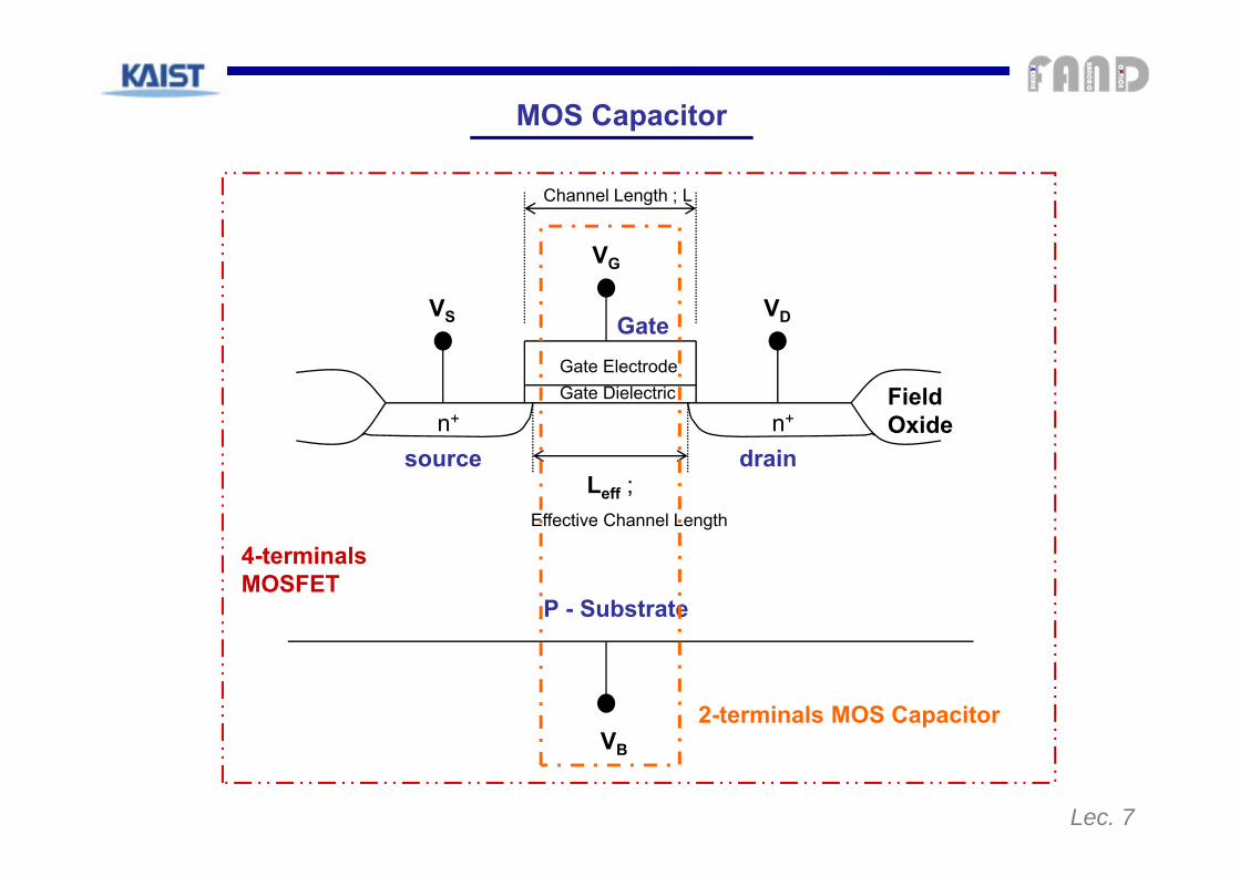
MOS Capacitor
Silicon dioxide
Modern MOSFET used 1nm SiO2 gate dielectric.
How many layers of Silicon dioxide layer?
25nm gate length MOSFET
Lec. 7
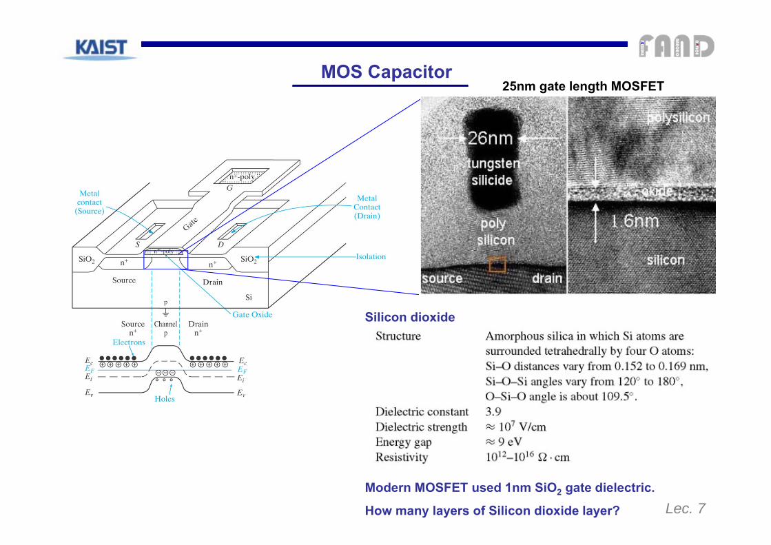
ii) To simplify the case, we assume
i) Real MOS case
sm No difference in work function
This is a Flat Band (FB) condition. Although it is not realistic, this assumptionwill simplify our approach.
MOS Band Diagram
p-
Lec. 7
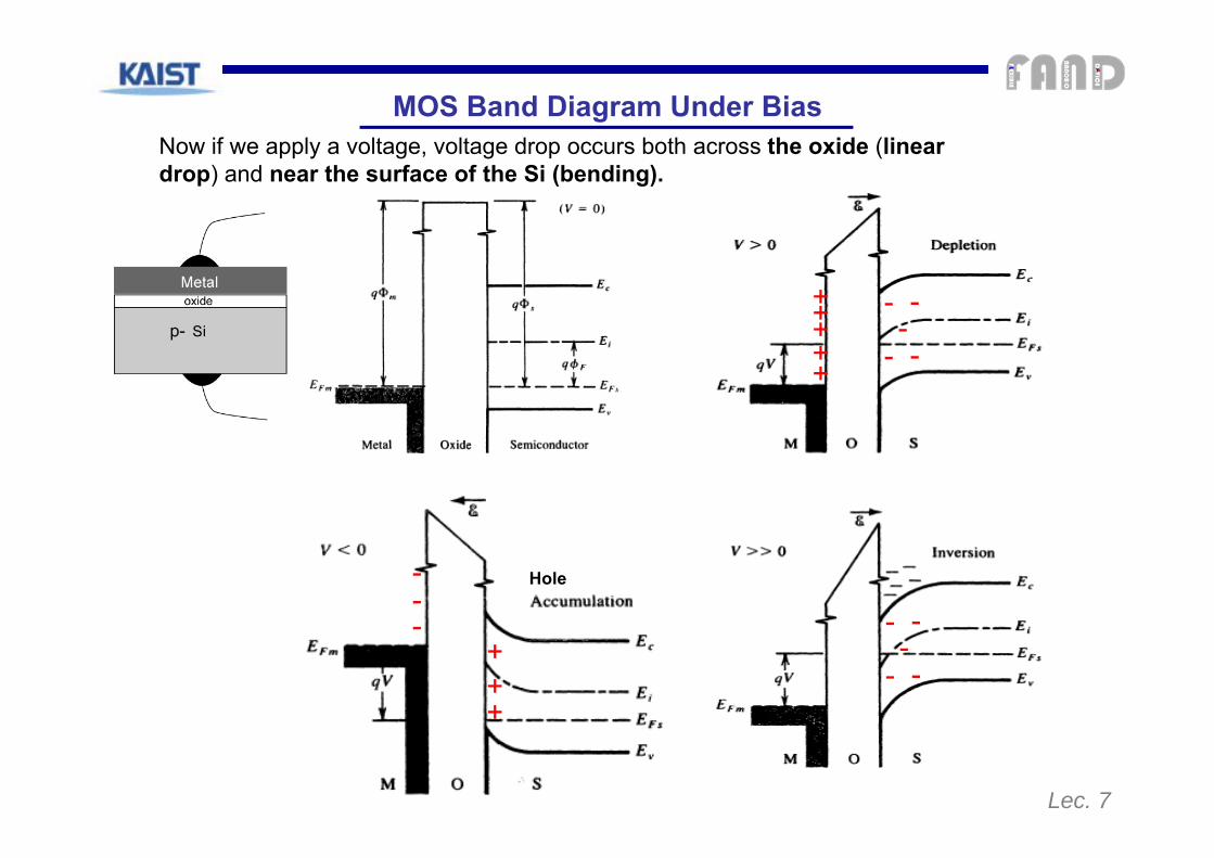
Now if we apply a voltage, voltage drop occurs both across the oxide (linear drop) and near the surface of the Si (bending).
Hole
+++
---
p-
MOS Band Diagram Under Bias
--
-
-
-+++
++
--
-
-
-

Lec. 7
Hole
+++
---
p-
Accumulation (Negative Bias to Gate)
• Accumulation of majority carriers at Si surface
The energy bands of Si near the surface bend upward.
Increased concentration of holes near the oxide/Si interface.
kTEEip
fienP /)(
sdxd
2
2
Vg<0
p-
Vg=0
sm , do not change with applied voltage.
No current through MOS structure, no change of Ef in semiconductor.

Lec. 7
p-
Depletion (Small Positive Bias to Gate)
--
-
-
-+++
++
Vg=0
Energy bands of Si at the surface bend downward as in Metal-Si contact.At the junction, majority carriers (holes) are depleted.
depletion region
WqN AchargeSpace
s
A
s
qNdxd
2
2
p-
Vg>0

Lec. 7
--
-
--
+++
++
p-
Inversion (Large Positive Bias to Gate)Vg>0
--
---
• The energy bands bend downwardeven further than depletion regime
Ei crosses over the Ef near the surface.
• Near the Si surface, (Ef-Ei)>0
At the surface, np>ni & np>pp.
kTEEip
ifenn /)(
p-
Vg>>0
+++
++
+++
++
• Inverted layer, separated from the underlying p-Si by depletion.

Lec. 7
If a bias is applied MOS, the voltage drop occurs across oxide and the depletion region of Si.
Sig VV
We define the onset of a strong inversion as follows:
region neutral in the )E(E : Si theof surface at the Potential :
ln22)(
fi
F
s
i
aFs n
Nq
kTinv
Thus, threshold voltage required for strong inversion is
i
si C
QV
Fi
dT C
QV 2
Threshold Voltage
Onset of strong inversion, there are negligible inversion charge (Qs=Qd)

Lec. 7
Once inversion condition is reached, e-
concentration near the surface increases very fast by even a small increase in band bending. Thus once an inversion layeris formed, the depletion layer width does not increases any more, that is, saturates at maximum value (Wm).
Charge per unit area in Si (QS):
),()(max
negativeareQQQWqNQQ
ns
mans Depletion layer
Inversion layer
Inversion chargeCharge in metal
(Qm is positive)
A
ias
A
Fs
A
ssm
A
ss
NqnNkT
qNqNinvW
qNW 2
)/ln(22)(2,2
W is same as n+ p junction
Inversion Charge & Depletion Width
21
max )(2 Fasad qNWqNQ )
21112(
/
dNaNqVW bis
ε

Lec. 7

Lec. 7
ionized acceptors
electron concentration
TG VV0 TG VV TG VV
FmE
FmE
CE CE
VE VEFE FEiE iE
FmE
QQ Q
x xxmaxQmaxQQ
dmaxx dmaxx
Threshold Voltage

Lec. 7
Inversion layer is less than 10nm.
Therefore we can neglect width of inversion layer in sketching electric field potential distribution.
nasm QWqNQQ max
Sig VV
i
si C
QV
Inversion
Fi
dT C
QV 2
These results are based on the assumption that Ef of metal and Si are equal.

Lec. 7
So far, we assume that Ef of Si and metal are equal. But this is not true for the most cases.
In addition to work function difference, MOS structure is affected by charges in insulator and interface. So we need to compensate this
assumption.
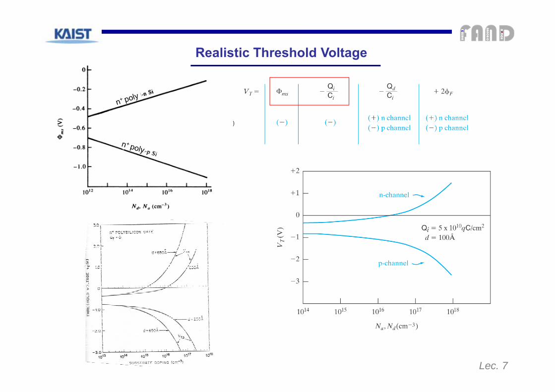
i
imsFB C
QV
FFsiAii
ms
Fi
d
i
imsT
qNQC
CQ
CQV
2))2(2(1
2
Realistic Threshold Voltage
(b)(a)
Work function difference
Interface charge
- Control of Vth: Gate materials, Ci control (thickness, high K), Threshold adjustment by ion implant (Na)
Lec. 7
Realistic Threshold Voltage

Lec. 7
p-Si
CV Characteristics
High freq.(1MHz)
Low freq. (1-100Hz)
MetalOxide
p-Si
_ MetalOxide
p-Si+ + ++ + - -- -
Ci CiCd
+
_
Capacitance decrease at 2, 3, 4 points means that depletion width is increasing.


![MOS Capacitor - Chenming Hu€¦ · 160 Chapter 5 MOS Capacitor n = N cexp[(E c – E F)/kT] would be a meaninglessly small number such as 10–60 cm–3. Therefore, the position](https://img.dokumen.tips/doc/110x75/5f069c847e708231d418da85/mos-capacitor-chenming-hu-160-chapter-5-mos-capacitor-n-n-cexpe-c-a-e-fkt.jpg)