Embed Size (px)
Citation preview
1
ELECTRIC FIELD AND TEMPERATURE EFFECTS ON ELECTRIC FIELD AND TEMPERATURE EFFECTS ON COPPER TRANSPORT IN MOS CAPACITOR WITH COPPER TRANSPORT IN MOS CAPACITOR WITH
COPPER AS THE GATE METAL COPPER AS THE GATE METAL
Prof. Yosi Shacham-DiamandWasedaWaseda UniversityUniversity

2
Surface resistance measurement
R/Ro Vs Oxidation time
0
0.5
1
1.5
2
2.5
3
3.5
0 200 400 600 800
Time (min)
R/R
o
CoMoP/Cu/CoMoPon Co seadCoWP/Cu/CoWP onCo seadCoWP/Cu/CoWP onCu seadCoMoP/Cu on Cusead

3
Co0.9W0.02P0.08
0 200 400 600
60
80
100
120
hcp Co + Co2Phcp Cohcp Co + amorph. Co
Cooling 1st Run
1st Run
2nd Run
Res
istiv
ity (µ
Ω·c
m)
Temperature (oC)
Heating rate ~ 2.8°C/min ; Vacuum ~ 5 × 10⁻⁶ Torr
Tracking structural changesIn-situ resistivity as a function of temperature
After anneal:Significant temperature independent
contribution to electron scattering
(imperfections including impurities)Co BulkFilm dT
d dTd ρ
=ρ
BulkFilm ρ>ρ
413.6 14.0 14.4
-14
-13
-12
-11
-10 460 440 420
104/Tc (K-1)
ln[(d
T/dt
)/Tc2 ] (
-)
Tc (oC)
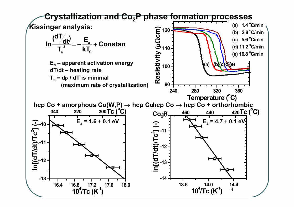
Ea – apparent activation energydT/dt – heating rateTc ≡ dρ / dT is minimal
(maximum rate of crystallization)
Constant kTE
T)dt
dT( ln
C
a2
C
+−=
240 280 320 36090
100
110
120
(e)(c)(d)(b)(a)
Res
istiv
ity (µ
Ωcm
)
Temperature (oC)
(a) 1.4 oC/min(b) 2.8 oC/min(c) 5.6 oC/min(d) 11.2 oC/min(e) 16.8 oC/min
Crystallization and Co2P phase formation processes
16.4 16.8 17.2 17.6 18.0-13
-12
-11
-10
340 320 300Tc (oC)
ln[(d
T/dt
)/Tc2 ] (
-)
104/Tc (K-1)
Ea = 1.6 ± 0.1 eV Ea = 4.7 ± 0.1 eV
hcp Co + amorphous Co(W,P) → hcp Cohcp Co → hcp Co + orthorhombic Co2P
Kissinger analysis:

5
[ ] )t-(tk(T)- exp - 1 )t(f n0⋅=
)0(tf(t)-1
)(tf(t) 1
=ρ+
∞→ρ=
ρ
n = a + b⋅ca = 1 ; Constant nucleation rate (N ~ t )b = 3 ; 3D growthc = 0.5 ; Diffusion controlled growth
0 10 20 30
100
110
120n2 n3n1
Res
istiv
ity (µ
Ω·c
m)
T ~ 260oC
Time (X103 sec)
f(t) – fraction crystallized
k (T) – apparent rate coefficientt0 – incubation timen – J-M-A index
Fraction crystallized as a function of time at a constant temperature:
Crystallization processJ-M-A analysis:
103 104
-4
-2
0
2
n1 = 1.5 ± 0.2
n2 = 2.6 ± 0.2
n3 = 1.3 ± 0.2
ln(-l
n(1-
f)) (-
)
Time (sec)

6
file: “S150n13500KleftisSiO2”
30 35 40 45 50 55
Siλ/2 (004)
εCo(01·0)
εCo(01·1) εCo
(00·2)
Difference
Co seed
Co0.9W0.02P0.08 as-dep.
Inte
nsity
(arb
. uni
ts)
2θ (°)
As-deposited structure?
Powder XRD, Bragg-Brentano geometry
I. Electroless Co0.9W0.02P0.08
II. Sputtered Co (2 nm thick)III. SiO2
Cross sectional phase contrast TEM image – as deposited film
Z.A. [00⋅1]
(10⋅0)
(12⋅0)–5 nm
I.
II.
III.
Fast Fourier transform

7
0 5 10 15 200.0
0.2
0.4
0.6
0.8
1.0
400oC300oC
l (nm)
α (-
)
8 at. % 10 at. % )
r1)
C1 - 1 (
r1(V
l4 )
rr()
C1 - 1 - (1
1 2pP
2Co
hcp2
p
Co
P
⋅++
⋅=α
α - Fraction coverage of the grain boundaryrCo – Atomic radius of CorP – Covalent radius of PCP – Atomic concentration of P in the filmVhcp – Volume of hcp unit cell
Estimation of grain boundary coverage by Passuming 1 ML of P enveloping hcp Co grains with a side length or diameter, l
Co - PEnrichment of P at the grain boundariesWhy does Co2P nucleate at ~ 420°C?

8
IntroductionIntroduction
Replacing Al with CuCu integration with ILD aroused some problems:
AdhesionCorrosionCu ions transport
The solution: Depositing CoWP as a thin diffusion barrier layer
How to evaluate the quality of the diffusion barrier?Electrical monitoring of MOS capacitorsBTS followed by electrical characterization
T e l A v i v U n i v e r s i t y

9
Ideal MOS CapacitorIdeal MOS Capacitor
Fig. 1: MOS Capacitor
Fig. 2: Energy Diagram of Ideal MOS Capacitor, V=0
Uniform dopingUniform doping
No Currents through the No Currents through the oxideoxide
ΦΦmsms=0=0
There are no oxide charges There are no oxide charges or interface onesor interface ones
Ohmic contact between the Ohmic contact between the semiconductor and the back semiconductor and the back contactcontact
T e l A v i v U n i v e r s i t y
10
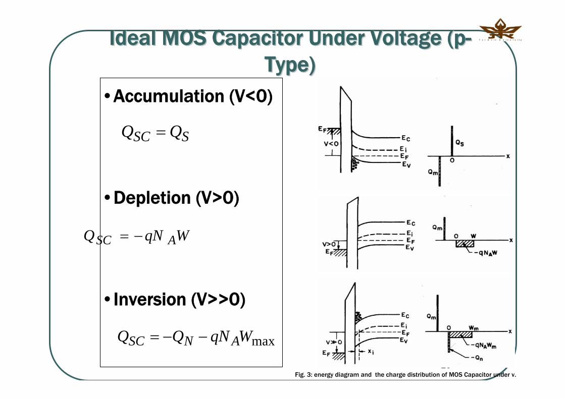
Ideal MOS Capacitor Under Voltage (pIdeal MOS Capacitor Under Voltage (p--Type)Type)
•Accumulation (V<0)
•Depletion (V>0)
•Inversion (V>>0)
WqNQ ASC −=
maxWqNQQ ANSC −−=
SSC QQ =
T e l A v i v U n i v e r s i t y
Fig. 3: energy diagram and the charge distribution of MOS Capacitor under v.

11
CC--V Configuration of an Ideal MOS V Configuration of an Ideal MOS Capacitor (pCapacitor (p--Type)Type)
BN0 CC1
C1
1C
++
=
CFB(ψs=0)
Fig. 5:HF C-V of MOS Capacitor
Fig. 4:The Equivalent Electrical Circuit of MOS Capacitor
OOxxiiddee
CCaapp
T e l A v i v U n i v e r s i t y
sOXG VV φ+=

12
CC--V Configuration of an Ideal MOS V Configuration of an Ideal MOS Capacitor (pCapacitor (p--Type)Type)
BN0 CC1
C1
1C
++
=
CFB(ψs=0)
Fig. 5:HF C-V of MOS Capacitor
Fig. 4:The Equivalent Electrical Circuit of MOS Capacitor
T e l A v i v U n i v e r s i t y
sOXG VV φ+=

13
CC--V Measurement (pV Measurement (p--type)type)
dVdQC =
Fig. 6:Low-frequency (LF), high frequency (HH) and deep depletion (DD) capacitance-voltage curves
Our COur C--V Measurement (nV Measurement (n--type)type)
T e l A v i v U n i v e r s i t y

14
Real MOS CapacitorReal MOS Capacitor
OX
sit
OX
Ot
OX
m
OX
fmsFB C
)(QCQ
CQ
CQV ψ
−γ
−γ
−−φ=
FBsOXG VVV +φ+=
( )⎪⎭
⎪⎬⎫
⎪⎩
⎪⎨⎧
=γ
=γ
=
=
1
0
)tx(
0x
ox
Fig. 8:The influence of oxide charges and the φms on the C-V curve.
Fig. 7:Charges and their location for thermally oxidized Si.
T e l A v i v U n i v e r s i t y

15
Real MOS Capacitor (pReal MOS Capacitor (p--type)type)
OX
sit
OX
Ot
OX
m
OX
fmsFB C
)(QCQ
CQ
CQV ψ
−γ
−γ
−−φ=
FBsOXG VVV +φ+=
( )⎪⎭
⎪⎬⎫
⎪⎩
⎪⎨⎧
=γ
=γ
=
=
1
0
)tx(
0x
ox
Fig. 8:The influence of oxide charges and the φms on the C-V curve.
T e l A v i v U n i v e r s i t y

16
CC--t Measurement & t Measurement & ZerbstZerbsttechniquetechnique
i' g sqndt −τ−=
Fig. 10:Space-charge region (SCR) and quasinetural region generation components of a
deep depletion MOS-C.
A0S
'OXiF
F
OX
A'g
i2
OXNK
SCn21
CC
CC
Nn2
CC
dtd
ε+⎟⎠⎞
⎜⎝⎛ −
τ=⎟
⎠⎞
⎜⎝⎛−
2OXC
Cdtd
⎟⎠⎞
⎜⎝⎛− ⎟
⎠⎞
⎜⎝⎛ −1
CCF
Fig. 11:Zerbst plot of the C-t transient
Fig. 9:Deep depletion MOS-C characteristics: (a) the C-V curve. (b) the C-t transient.
T e l A v i v U n i v e r s i t y
)C/C()n/N(t
FOiDF'
g ⋅≈τ

17
CC--t Measurementt Measurement
Fig. 9:Deep depletion MOS-C characteristics: (a) the C-V curve. (b) the C-t transient.
T e l A v i v U n i v e r s i t y
)C/C()n/N(t
FOiDF'
g ⋅≈τ

18
ZerbstZerbst techniquetechnique'
i'g
FiN sqn)WW(qndt
dQ−
τ
−−=
Fig. 11:Zerbst plot of the C-t transient
T e l A v i v U n i v e r s i t y
A0S
'OXiF
F
OX
A'g
i2
OXNK
SCn21
CC
CC
Nn2
CC
dtd
ε+⎟⎠⎞
⎜⎝⎛ −
τ=⎟
⎠⎞
⎜⎝⎛−
2OXC
Cdtd
⎟⎠⎞
⎜⎝⎛− ⎟
⎠⎞
⎜⎝⎛ −1
CCF

19
Barrier integrity
Questions:
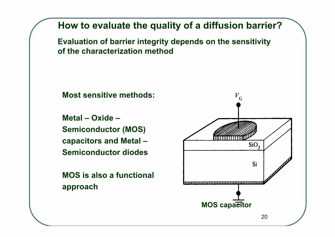
1.How to evaluate the quality of a diffusion barrier?
2.What is the barrier integrity of electroless deposited Co alloy films?
20
Evaluation of barrier integrity depends on the sensitivity of the characterization method
How to evaluate the quality of a diffusion barrier?
MOS capacitor
Most sensitive methods:
Metal – Oxide –Semiconductor (MOS) capacitors and Metal –Semiconductor diodes
MOS is also a functional approach

21
Evaluation of D.B. quality using MOS capacitors: Capacitance-Voltage
∆VFB Cu+ ions in the oxide – requires electric field in order to enhance drift of Cu+ ions→ ∆VFB<0
CINV Decreased minority lifetime as a result of Cu generated deep levels→ CINV increases for a fixed a.c. frequency
f otfb
O
mms
Q QV - CQφ + +
=
-3 -2 -1 0 1 2 3
5
10
15
20
25
30
35
300°C / 30 min 450°C / 4 hrs 450°C / 12 hrs
Cap
acita
nce
(pF)
Voltage (V)
∆Vfb
CINVCu/Co0.9P0.1
Quasi – static C-V measurements (1 MHz)

22
0.0 0.1 0.2 0.3 0.4 0.5 0.60.00
0.05
0.10
0.15
0.20
MOS5_5_1 CoP/Cu/CoP 300C/30min CV1+Ct1
τ' = 630 ± 50 µsecs' = 0.08 ± 0.01 cm/sec
-d(C
0/C)2 /d
t (s
ec-1)
CF/C - 1 (-)
Time
Zerbst plot of a C-t measurement
Cu/Co0.9P0.1 after 300°C /30min
0 50 100 150 200 2505
6
7
8
9
10
Cap
acita
nce
(pF)
Time (sec)
300°C / 30 min 450°C / 4 hrs 450°C / 12 hrs
Inversion
Deep depletion
Evaluation of D.B. quality using MOS capacitors: Capacitance-transient
slopeCNCn2 '
FB
0ig ⋅=τFrom the slope:Effective generation lifetime:
0i
B0S
Cn2interceptNεK s' ⋅
=From the intercept:Effective generation velocity:
∫=W
WscrN
F
dxG q- scr) (bulk dt/dQ
Cu/Co0.9P0.1
Capacitance time measurements (1 MHz)

23
bb
1 – Evaluated by C-t2 – Evaluated by C-V
Evaluation of diffusion barrier quality Results
A. Kohn, M. Eizenberg, Y. Shacham-Diamand
B. Israel, and Y. Sverdlov
Microelectronic Eng. 55, 297 (2001)
Electroless Co0.9P0.1 , 30 nm thick, are stable barriers at 450°C during approximately 10 hours
Current allowed total thermal budget: Thermal cycles equivalent to 400°C, 10 – 60 minutes
Barrier
30 nm thick
Thermal Stress1 Bias and Thermal Stress2
1 MV/cm at 300ºC / 30 min
Co0.96W0.04 Fails after 450ºC / 1hr Fails
Co0.9P0.1 Fails after 450ºC / 10 hr Stable
Co0.9W0.02P0.08 400ºC/30 min: Stable
500ºC/30 min: Fails
N/A

24
Investigation of the structure of electroless Co alloys and its evolution as a result of heat treatments
Questions:1. What is the as-deposited structure?
2. How does the structure change with thermal anneal?
3. What is the structure during failure of the diffusion barrier?
Case study: Co0.9W0.02P0.08Electroless Co0.9W0.02P0.08 10 – 100 nm
Sputtered Co or Cu 2 – 20 nm
(Sputtered Ti) (5 nm)
SiO2 100 nm
Si wafer

25
Most sensitive method: Metal Oxide Semiconductor (MOS) and Metal Semiconductor diodesMOS is also a functional approach
Evaluation of barrier integrity depends on the sensitivity of the characterization method
How to evaluate the quality of a diffusion barrier?
MOS structure

26
Evaluation of D.B. quality using MOS diodes: Capacitance-Voltage
∆VFB Cu+ ions in the oxide→ ∆VFB<0
Cinversion Decreased minority lifetimeas a result of Cu generated deep levels→ increases for a fixed a.c. frequency
Requires electric fieldIn order to enhance drift of Cu+
ions

27
-4 -2 0 2 4
20
40
60
80
Al/SiO2 TS Capacitor 33A no.1
Cap
acita
nce
(pF)
Voltage (Volts)
Vacuum anneal TS 300oC/30 min
-4 -2 0 2 4
20
40
60
80
Al/SiO2 BTS Capacitor 33A no.2
Cap
acita
nce
(pF)
Voltage (Volts)
Vacuum anneal BTS 300oC
2MV/cm 30 min
-4 -2 0 2 4
20
40
60
80
Cap
acita
nce
(pF)
Voltage (Volts)
CV Thermal stress Cap 33B n5 Cu/SiO2
Vacuum anneal TS 300oC/30min
-8 -4 0 4
20
40
60
CV BTS Cap 33B n4 Cu/SiO2
Cap
acita
nce
(pF)
Voltage (Volts)
Vacuum anneal BTS 300oC
2-0.5 MV/cm 30min
Equilibrium capacitance voltage measurements at 1 MHz
Applying bias –enhanced drift of Cu+, and degradation of the dielectric
Reference: Al / SiO2 / n-Si
Cu / SiO2 / n-Si

28
Deep depletion
Strong inversion
Accumulation
0
VG
0
+
t
Evaluation of D.B. quality using MOS diodes: Transient Capacitance

29
Deep depletion MOS-capacitor• Using the expression for capacitance as a function of gate voltage and inversion capacita• For a pulsed capacitor, where dVG/dt = 0,
(dQN/dt ~ -d(Co/C)2/dt)
Thermal generation of electron-hole pairs:
Generation of minority charge carriers
C - capacitance (F/cm2)Co- oxide capacitance (F/cm2)eo - permittivity of free space (F/cm)NB- net doping concentration (cm-3)ni - intrinsic carrier concentration (cm-3)KS- s.c. dielectric constant (Si:11.8) (-)QN- electron surface charge density (Cb/cm2)GSCR- steady-state scr generation rate (cm-3s-1)W - scr width (cm)WF - final scr width for MOS capacitor in heavy inversion (cm)tg - generation lifetime (sec)
30
0 50 100 150 200 250 300 3505
6
7
8
9
10
Cap
acita
nce
(pF)
MOS5_1 CoP/Cu/CoP 300C/30min Ct9
Time (sec)
Zerbst plot of the C-t transientExample: Cu/Co0.9P0.1 after 300°C /30min
0.0 0.1 0.2 0.3 0.4 0.5 0.6 0.70.00
0.05
0.10
0.15
0.20τ' = 930 ± 50 µsecs' = 0.10 ± 0.01 cm/sec
MOS5_1 CoP/Cu/CoP 300C/30min CV11+Ct9
-d(C
0/C)2 /d
t (s
ec-1)
CF/C - 1 (-)
Time
B0S
0iF
gFB
0i2
o
NεKs'Cn2 ) 1 -
CC()
'CNCn2 (
dt/C)d(C
+⋅τ
=−
slopeCNCn2 '
FB
0ig ⋅=τFrom the slope:
0i
B0S
Cn2intercept NεK s' ⋅
=From the intercept:
Inversion
Deep depletion
31
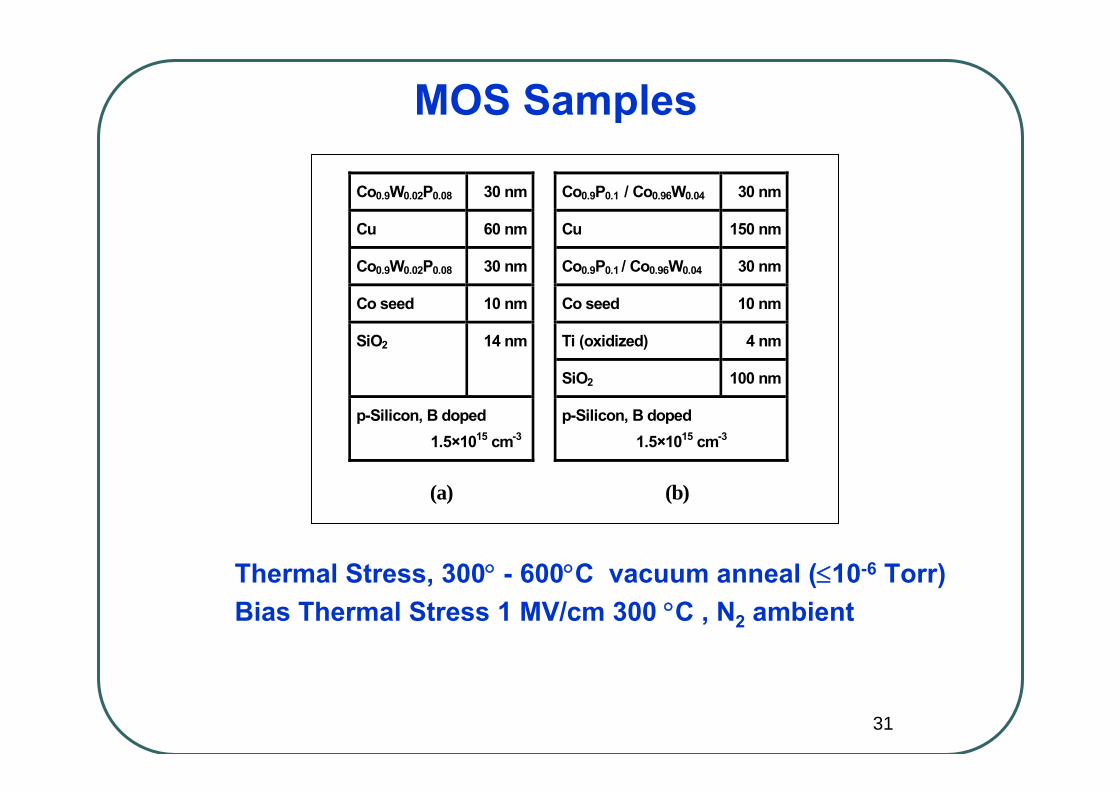
MOS Samples
Thermal Stress, 300° - 600°C vacuum anneal (≤10-6 Torr)Bias Thermal Stress 1 MV/cm 300 °C , N2 ambient
Co0.9W0.02P0.08 30 nm Co0.9P0.1 / Co0.96W0.04 30 nm
Cu 60 nm Cu 150 nm
Co0.9W0.02P0.08 30 nm Co0.9P0.1 / Co0.96W0.04 30 nm
Co seed 10 nm Co seed 10 nm
Ti (oxidized) 4 nmSiO2 14 nm
SiO2 100 nm
p-Silicon, B doped 1.5×1015 cm-3
p-Silicon, B doped 1.5×1015 cm-3
(a) (b)

32
-3 -2 -1 0 1 2 35
10
15
20
25
300oC / 30 min +450oC / 30 min
Cap
acita
nce
(pF)
Voltage (V)-3 -2 -1 0 1 2 3
5
10
15
20
25
30
35
C
apac
itanc
e (p
F)
Voltage (V)
300oC / 30 min +450oC / 30 min
Evaluation of diffusion barrier quality – 450°CCo0.96W0.04
diffusion barrier Typical example
p-Si
SiO2
Co0.96W0.04
Cu
Co0.96W0.04
Quasi – static capacitance voltage measurements at 1 MHz

33
0 40 80 120 1604
5
6
7
8
300oC / 30 min +450oC / 30 minC
apac
itanc
e (p
F)
Time (sec)
Evaluation of diffusion barrier quality – 450°C
p-Si
SiO2
Co0.96W0.04
Cu
Co0.96W0.04
Co0.96W0.04
diffusion barrier
0 50 100 150 2004
8
12
16
20
C
apac
itanc
e (p
F)
Time (sec)
300oC / 30 min +450oC / 30 min
Typical example
Capacitance transient measurement at 1 MHz

34
-3 -2 -1 0 1 2 3
5
10
15
20
25
30
35
300°C / 30 min 450°C / 4 hrs 450°C / 12 hrs
Cap
acita
nce
(pF)
Voltage (V)0 50 100 150 200 250
5
6
7
8
9
10
C
apac
itanc
e (p
F)
Time (sec)
300°C / 30 min 450°C / 4 hrs 450°C / 12 hrs
Evaluation of diffusion barrier quality – 450°C
Co0.9P0.1
diffusion barrierp-Si
SiO2
Co0.9P0.1
CuCo0.9P0.1
Typical example

35
0 2 4 6 8 10 120.0
0.1
0.2
0.3
0.4
(+order of magnitude)
Anneal time (hr)
Significant increase
V S' (c
m/s
ec)
0 2 4 6 8 10 120
200
400
600
800
Anneal time (hr)
τ g' (µ
sec)
Evaluation of diffusion barrier quality – 450°CTypical example
0 2 4 6 8 10 12-200-150-100-50
050
100150
∆VFB
(mV)
Anneal time (hr)
p-Si
SiO2
Co0.9P0.1
CuCo0.9P0.1

36
-4 -2 0 2 4
5
10
15
20
25
30
Thermal anneal +BTS
Cap
acita
nce
(pF)
Voltage (V)-4 -2 0 2 4
0
10
20
30
Thermal anneal +BTS
Cap
acita
nce
(pF)
Voltage (V)
Quasi-static C-V measurements of MOS capacitors at 1 MHz
Co0.9P0.1 Co0.96W0.04
Bias Thermal Stress - 300oC / 0.5 hr 1 MV/cm, N2 environment :Co0.9P0.1 diffusion barrier stable Co0.96W0.04 diffusion barrier fails
Typical example

37
T
Lower metal layer
Upper metal layer
Interconnectmetal layer
W S
P
CLL
CV = CLG
)TL
P4L ( k 2 RC 2
2
2
2
0 += ερ
ρ – metal resistivity; ε0 – vacuum permittivity; k – relative dielectric constantL – line length; P – line pitch; W – line widthS – line spacing; T – line thickness (the dielectric thickness above and below the interconnect is equal)
0.65 0.5 0.35 0.25 0.18 0.13 0.10
10
20
30
40Gate with Al/SiO2
Gate with Cu/low K
Gate
Del
ay (p
Sec)
Generation
Gate Delay Interconnect Delay: Cu/low K Interconnect Delay: Al/SiO2 Sum of Delays: Cu/low K Sum of Delays: Al/SiO2
Al 3.0 µΩ⋅cm ; Cu 1.7 µΩ⋅cm SiO2 K=4.0 ; Low K K=2.0Al+Cu 0.8 µm thick, 436 µm long
Mark T.Bohr, Interconnect Scaling -The Real Limiter to High Performance ULSII995 International Electron Devices Meeting Technical Digest, (1995) 241-244.
Motivation for Cu metallizationI. Reducing the RC delay time
38
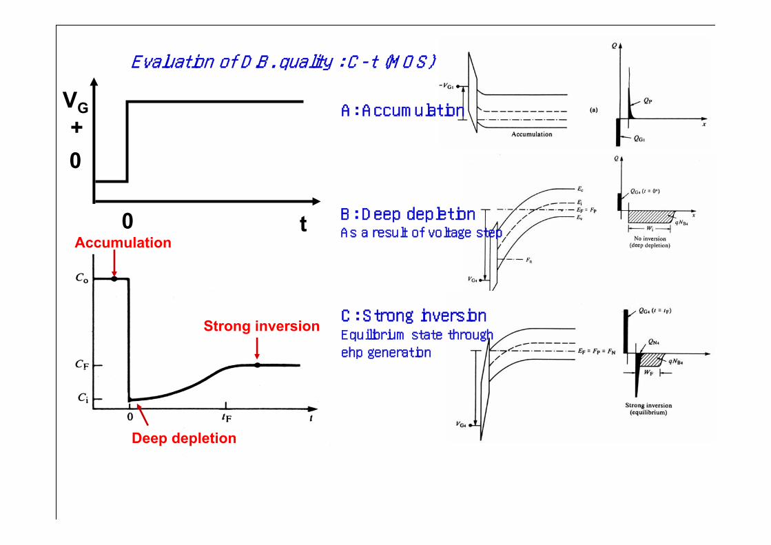
Evaluation of D.B. quality : C-t (MOS)
A: Accumulation
B: Deep depletionAs a result of voltage step
C: Strong inversionEquilibrium state throughehp generation
Deep depletion
Strong inversion
Accumulation
VG
0
0
+
t

39
Electroless deposition of Co alloysProcess:
Co(II)Cit + e- → Co(I)CitadsCo(I)Citads + e- → Co(s) + Cit
Reduction of Co ions (complexed with the citrate)
H2PO2- → HPO2
-ads +
Hads
Reducing agent is hypophosphite:H ?extraction? on the catalytic seed layer
Reaction with OH- ions:
HPO2-ads + OH- → H2PO3
- + e-
Reaction of H atoms is dependant on the catalytic seed layer:
Hads + OH- → H2O + e- Catalytic seed layer: Pd, Pt, Rh 2Hads → H2 Catalytic seed layer: Cu, Au, Ag
In parallel, a competing reaction of hypophosphdeposits P:
H2PO2- + 2H+ + e- → P +
H2O
W deposition? Induced co-deposition: iron group ion + refractory metalProposed Mechanism: Podlaha et al., J. Electrochem. Soc. 144 (1997) 1672
Induced co-deposition of MoO42- and ion M (Fe2+, Co2+, Ni2+) complexed with a ligand L
MoO42- + M(II)L + 2H2O + 2e- → [M(II)LMoO2]ads + 4OH-
[M(II)LMoO2]ads + 2H2O + 4e- → Mo(s) + M(II)L + 4OH-

40
Periodicity in P depth profile
AES depth profiles
SiSiO2
TiCo
Co0.9W0.02P0.08
as-deposited
3000C
5000C
7000C
4000C
~12 nm

41
Chemical binding statesCo, W – no observable change in chemical binding (XPS, EELS)P – significant changes
X-ray photoelecton spectroscopySuggested fitting of 2p3/2 and 2p1/2 P states :P1 and P2 2p binding states1. p3/2 and p1/2 ∆E = 0.84 eV Goodman et al., Phys. Rev B 27, 7440 (1983)2. p3/2 and p1/2 area ratio = 2:13. FWHM, G/L ratio equal for p3/2 and p1/2 for P1, P24. 0.2 ≤ G/L ≤ 0.8Results:1. P1 and P2 – equal B.E., FWHM, G/L ratio for all samples
→ validates assumptions2. Area ratio of P1:P2 → ratio of binding states
as-dep Data Fitting
P2
P2
P1P1
400oC
P1 P1P2
P2
P1 P1P2
P2
600oC
132 130 128 126
P1P1P2
P2
Co2P
Binding Energy (eV)
Inte
nsity
(arb
. uni
ts)
Sample
Area ratio P1/P2 (-) ±10%
Co0.9W0.02P0.08 as-dep 1:1.1 Co0.9W0.02P0.08 400oC 1:2 Co0.9W0.02P0.08 600oC 1:4.9 Co2P Reference 1:5

42
Same results on Co and Cu seed layer
No phase reaction between Cu and the electroless film up to 700°C
Structure of Co0.9W0.02P0.08 and its evolution with thermal treatmentsCu : Influence of seed layer and / or phase interaction?
Powder XRD, Bragg-Brentano geometry
Thermal anneal:1 hourVacuum ≤ 10-6
Torr
Copper seed
30 35 40 45 50 55
5x10²
2x10³
3x10³
4x10³
5x10³
2θ (°)
as depInte
nsity
(a.u
.)
300oC
500oC
700oC
Cu (111)
αCo(200)
εCo(01·1)
Co2P (201)
Siλ/2 (004) αCo
(111)
εCo (00·2)
εCo (01·0)

43
The Main GoalsThe Main Goals
The effectiveness of CoWP as a Barrier The effectiveness of CoWP as a Barrier Layer against Cu transportLayer against Cu transport
Failure characterizationFailure characterization
Comparison between the various kinds of Comparison between the various kinds of electrical measurements electrical measurements
The effect of the temperature and the bias The effect of the temperature and the bias on the Cu transporton the Cu transport
Calculation of the Calculation of the DDeffeff of Cu under BTS of Cu under BTS

44
CapacitorsCapacitors’’ typetype
Oxide
Semiconductor
Metal
n-Si-360µ
SiO2-1000Å
CoWP-300Å
Cu-600Å
CoWP-300Å
Al-1000Å
Co-100Å
Ti-20Å
1. Test capacitors: CoWP/Cu/CoWP/Co/Ti/SiO2 2. Reference capacitors #1: CoWP/Cu/Co/Ti/SiO23. Reference capacitors #2: CoWP/Cu/SiO2

45
Experimental SetupExperimental Setup
Annealing at 300°C for 1/2hr
Annealing at 300°C for 1/2hr
performing C-V, C-t and I-VMeasurements at 25°C
performing CC--VV, CC--tt and II--VVMeasurements at 25°C
I-t measurement in-situ
II--tt measurement in-situ
Going down to room temperature and performing C-V, C-t and I-V measurements
Going down to room temperature and performing CC--VV, CC--tt and II--VV measurements
BTS at 250-300°C, undervarious fields; 0.3-1.4MV/cm
BTSBTS at 250-300°C, undervarious fields; 0.3-1.4MV/cm
The main parameters, that were derived from the electrical measurements, are:
CC--VV curve: CFB, Nd, Qit, Qm, dox
CC--tt curve: τg’, s’
II--VV curve: Ecritical, Conduction mechanism,
II--tt curve: tf, Leakage currents

46
Results presentation methodologyResults presentation methodology
I. TS and BTS measurements under:
low electriclow electric fieldfield.
high electric fieldhigh electric field.
II. Data of BTS results under wide range of temperatures and fields.
III. Calculating the effective diffusion coefficient
IV. Proposing a model for Cu+ transport in the oxide.

47
Results presentation methodologyResults presentation methodology
I. TS and BTS measurements under:
low electriclow electric fieldfield.
high electric fieldhigh electric field.
II. Data of BTS results under wide range of temperatures and fields.
III. Modeling using the effective diffusion coefficient
IV. Proposing a model for Cu transport in the oxide.

48
CC--VV of test cap.: CoWP/Cu/CoWP/Co/Ti/SiOof test cap.: CoWP/Cu/CoWP/Co/Ti/SiO22
TS4/BTS497
TS3/BTS325.83
TS2/BTS22.5
TS1/BTS11
Stress No.Accumulate Time(hr)
-2.5 -2.0 -1.5 -1.0 -0.5 0.0 0.5 1.0
0
50
100
150
200
250
300
350
400
b
C(pF)
V(v)
PreAnn. TS1 TS4
-10 -8 -6 -4 -2 0 2 4
0
50
100
150
200
250
300
350
400
a
C(pF)
V(v)
PreAnn. TS1 TS4
TS: 250TS: 250°°CC
-10 -8 -6 -4 -2 0 2 4
0
50
100
150
200
250
300
350
400
a
C(pF)
V(v)
PreAnn. BTS1 BTS2 BTS3 BTS4
-2.5 -2.0 -1.5 -1.0 -0.5 0.0 0.5 1.0
0
50
100
150
200
250
300
350
400
b
C(pF)
V(v)
PreAnn. BTS1 BTS2 BTS3 BTS4BTS: 250BTS: 250°°C, C,
0.3MV/cm0.3MV/cm

49
∆∆VVFBFB vs. timevs. time of ref. #1 of ref. #1
0 10 20 30 40 50-0.7
-0.6
-0.5
-0.4
-0.3
-0.2
-0.1
0.0
0.1
0.2
VFB [V]∆
time [hr]
TS BTS
0 5 10 15 20 25 30 35 40 4545
50
55
60
65
70
75
80
85
90
a
C(pF)
t(sec)
PreAnn. BTS1 BTS2 BTS3 BTS4 BTS5 BTS6
0 0.05 0.1 0.15 0.2 0.25 0.3 0.35 0.4 0.45
0
0.5
1
1.5
2
2.5Zerbst Plot
(Cf/C -1)[-]
-d(C
o/C
)2 /dt,
[1/s
ec]
t=26.12 1e-6 sec
Vs=0.63457 cm/sec
b
PreAnn.τg
'=26 µsS'=0.63 cm/sec
cd
CC--t t of ref. #1 under BTS: 250of ref. #1 under BTS: 250°°C, 0.3MV/cmC, 0.3MV/cm
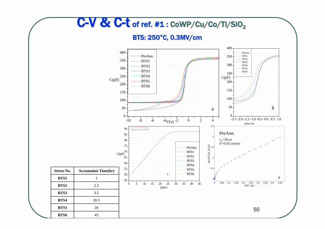
50
CC--V & CV & C--tt of ref. #1 :of ref. #1 : CoWP/Cu/Co/Ti/SiOCoWP/Cu/Co/Ti/SiO22
-10 -8 -6 -4 -2 0 2 40
50
100
150
200
250
300
350
400
a
C(pF)
V(v)
PreAnn. BTS1 BTS2 BTS3 BTS4 BTS5 BTS6
-2.5 -2.0 -1.5 -1.0 -0.5 0.0 0.5 1.00
50
100
150
200
250
300
350
400
b
C(pF)
V(v)
PreAnn. BTS1 BTS2 BTS3 BTS4 BTS5 BTS6
45BTS6
26BTS5
20.5BTS4
3.5BTS3
2.5BTS2
1BTS1
Accumulate Time(hr)Stress No.
BTS: 250BTS: 250°°C, 0.3MV/cmC, 0.3MV/cm
0 5 10 15 20 25 30 35 40 4545
50
55
60
65
70
75
80
85
90
a
C(pF)
t(sec)
PreAnn. BTS1 BTS2 BTS3 BTS4 BTS5 BTS6
0 0.05 0.1 0.15 0.2 0.25 0.3 0.35 0.4 0.45
0
0.5
1
1.5
2
2.5Zerbst Plot
(Cf/C -1)[-]
-d(C
o/C
)2 /dt,
[1/s
ec]
t=26.12 1e-6 sec
Vs=0.63457 cm/sec
b
PreAnn.τg
'=26 µsS'=0.63 cm/sec
cd
51
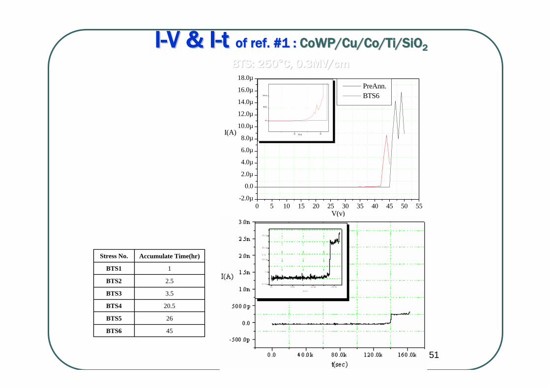
II--V & IV & I--t t of ref. #1 :of ref. #1 : CoWP/Cu/Co/Ti/SiOCoWP/Cu/Co/Ti/SiO22
45BTS6
26BTS5
20.5BTS4
3.5BTS3
2.5BTS2
1BTS1
Accumulate Time(hr)Stress No.
0 5 10 15 20 25 30 35 40 45 50 55-2.0µ
0.0
2.0µ
4.0µ
6.0µ
8.0µ
10.0µ
12.0µ
14.0µ
16.0µ
18.0µ
20 40
0.0
200.0n
I(A)
V(v)I(A)
V(v)
PreAnn. BTS6
BTS: 250BTS: 250°°C, 0.3MV/cmC, 0.3MV/cm

52
CC--V & IV & I--tt of ref. #2: CoWP/Cu/SiOof ref. #2: CoWP/Cu/SiO22
8BTS6
6BTS5
4BTS4
3BTS3
1.5BTS2
0.5BTS1
Accumulate Time(hr)Stress No.
BTS: 250BTS: 250°°C, 0.3MV/cmC, 0.3MV/cm
-2.5 -2.0 -1.5 -1.0 -0.5 0.0 0.5 1.050
100
150
200
250
300
350
400
b
C(pF)
V(v)
Theory PreAnn. BTS1 BTS2 BTS3 BTS4 BTS5 BTS6
-10 -8 -6 -4 -2 0 2 450
100
150
200
250
300
350
400
a
C(pF)
V(v)
Theory PreAnn. BTS1 BTS2 BTS3 BTS4 BTS5 BTS6

53
Temperature effect under Temperature effect under lowlow electric fieldelectric fieldin ref. #1in ref. #1
250 275 3000.0
0.1
0.2
0.3
0.4
0.5
0.6
VFB| [V]|∆
T(C0)
A B
0 10 20 30 40 50
-0.6
-0.5
-0.4
-0.3
-0.2
-0.1
0.0
0.1
0.2
∆VFB [V]
time [hr]
TS=2500C TS=2750C BTS=2500C, 0.3MV/cm BTS=2750C, 0.3MV/cm BTS=3000C, 0.3MV/cm
-0.5729.38B300°C ,0.3MV/cm3
-0.3233.50B
-0.2519.15A275°C ,0.3MV/cm2
-0.2026.00B
-0.1520.50A250°C ,0.3MV/cm1
∆VFB(V))hr(Stress timetypeBTS
* * AA--flatflat--band shift after 20 hours.band shift after 20 hours.
* B* B--critical change in the Ccritical change in the C--V curve after 26V curve after 26--33 hours33 hours..

54
Results presentation methodologyResults presentation methodology
I. TS and BTS measurements under:
low electriclow electric fieldfield.
high electric fieldhigh electric field.
II. Data of BTS results under wide range of temperatures and fields.
III. Modeling using the effective diffusion coefficient
IV. Proposing a model for Cu transport in the oxide.

55
CC--V, CV, C--t & It & I--t t of ref. #1: of ref. #1: CoWP/Cu/Co/Ti/SiOCoWP/Cu/Co/Ti/SiO22
2.2hrBTS4
22.5BTS3
9.5BTS2
4.5BTS1
Accumulate Time(min)Stress No.
BTS: 250BTS: 250°°C, 1.2MV/cmC, 1.2MV/cm
-45 -40 -35 -30 -25 -20 -15 -10 -5 0 5 10 150
50
100
150
200
250
300
350
400
a
C(pF)
V(v)
PreAnn. BTS1 BTS2 BTS3 BTS4
-2.5 -2.0 -1.5 -1.0 -0.5 0.0 0.5 1.00
50
100
150
200
250
300
350
400
b
C(pF)
V(v)
PreAnn. BTS1 BTS2 BTS3 BTS4
0 20 40 60 80 100 120 140
50
100
150
200
250
300
a
C(pF)
t(sec)
PreAnn. BTS1 BTS2 BTS3 BTS4
c0 0.1 0.2 0.3 0.4 0.5 0.6 0.7
0
0.1
0.2
0.3
0.4
0.5
0.6
0.7
0.8Zerbst Plot
(Cf/C -1)[-]
-d(C
o/C
)2 /dt,
[1/s
ec]
t=143.8209 1e-6 sec
Vs=0.47689 cm/sec
b d
PreAnn.τg
'=143 µsS'=0.48 cm/s
e

56
CC--V & IV & I--t t of test cap.:of test cap.: CoWP/Cu/CoWP/Co/Ti/SiOCoWP/Cu/CoWP/Co/Ti/SiO22
BTS: 250BTS: 250°°C, 1.2MV/cmC, 1.2MV/cm
-10 -8 -6 -4 -2 0 2 4
0
50
100
150
200
250
300
350
400
C(pF)
V(v)
PreAnn. BTS
*BTS - accumulate stress time of 27.5hr

57
CC--V V of ref. #2:of ref. #2: CoWP/Cu/SiOCoWP/Cu/SiO22
BTS437.66
BTS322.33
BTS29
BTS14.5
Stress No.Accumulate Time(min)
BTS: 250BTS: 250°°C, 1.2MV/cmC, 1.2MV/cm
-2.5 -2.0 -1.5 -1.0 -0.5 0.0 0.5 1.050
100
150
200
250
300
350
400
C(pF)
V(v)
PreAnn. BTS1 BTS2 BTS3 BTS4
-10 -8 -6 -4 -2 0 2 450
100
150
200
250
300
350
400
C(pF)
V(v)
PreAnn. BTS1 BTS2 BTS3 BTS4
5.31·108
2.51·107
Cu+[ions/cm2·sec]
1.2·10121.2MV/cm
7.24·10110.3MV/cm
Cu+[ions/cm2]E
0.05.0k 10.0k15 .0k20.0k 25.0k30.0-6-5-4-3-2-1V FB [V]∆ time( sec) [ ] overall2 tSlopeAqcmCu ∆⋅⋅⋅−=⎥⎦⎢⎣ dtSlope=
∆∆VVFB FB vs. timevs. time of ref. #2 under low and high electric fieldof ref. #2 under low and high electric field

58
Temperature effect under Temperature effect under highhigh electric fieldelectric fieldin ref. #1in ref. #1
9.16min10-2A16.5min-8.32300°C 1MV/cm
3
31.28min10-2A40min-9.29275°C 1MV/cm
2
3.99hr10-2A4.05hr-12.61250°C 1MV/cm
1
Arrival time to the current threshold
Current threshold
Arrival time to a significant
shift
∆VFB
From I-tFrom C-VBTS
02468
10121416182022
300275250
|∆VFB| [V]
T(C0)
0 1 2 3 4
-10-9-8-7-6-5-4-3-2-101
time [hr]
∆VFB [V]
BTS=2500C, 1MV/cm BTS=2750C, 1MV/cm BTS=3000C, 1MV/cm

59
Electric field effect on the Electric field effect on the flatbandflatband shift in ref. #1 and shift in ref. #1 and #2#2
0 5 10 15 20 25 30 35
-10-9-8-7-6-5-4-3-2-101
VFB [V]∆
time(hr)
Cu/SiO2=0.3MV/cm,2500C
Cu/Co/Ti/SiO2=0.3MV/cm,2500C
Cu/SiO2=1.2MV/cm,2500C
Cu/Co/Ti/SiO2=1.2MV/cm,2500C
Cu/Co/Ti/SiO2=1MV/cm,2500C
High
LowCu/SiO2
High
Low
Electric field
strength
Cu/Co/Ti/SiO2
Advance stress time
Initial stress time
type
Gradual increase in ∆VFB
Exponential increase in ∆VFB
••Under low electric field the flat band Under low electric field the flat band shift is gradualshift is gradual
••The CO/Ti seed layer serves as a barrier The CO/Ti seed layer serves as a barrier layer against Cu at low electric fieldslayer against Cu at low electric fields

60
Our observations concerning to the electric field and Our observations concerning to the electric field and temperaturetemperature
Capacitors without a barrier layer (ref. #2):lllLinear increase in the flat band shift under low and high IIIelectric fields.
Capacitors with a seed layer (ref. #1):lllLinear increase in the flat-band shift only under low IIIelectric fields. A sudden increase in progress steps of IIIthe BTS under high electric fields.
Capacitors with the full stack (test cap.) or capacitors IIIthat were subjected to TS only:lllMinor shifts.
The temperature effect becomes significant in a lower IIIvalue at BTS under high electric field, comparing to IIIBTS under low electric field.

61
Results presentation methodologyResults presentation methodology
I. TS and BTS measurements under:
low electriclow electric fieldfield.
high electric fieldhigh electric field.
II. Data of BTS results under wide range of temperatures and fields.
III. Modeling using the effective diffusion coefficient
IV. Proposing a model for Cu transport in the oxide.

62
BTS under different kind of fields and temperaturesBTS under different kind of fields and temperatures
kTQ
GGf e
Vd
Vdt
0
22
µ=
µ=
1.7x10-31.8x10-31.8x10-31.8x10-31.9x10-31.9x10-32.0x10-3102
103
104
105
106
T [0C]
tƒ [sec]
1/T [k-1]
E=0.3MV/cm E=0.6MV/cm E=1.0MV/cm E=1.2MV/cm
2500C2750C3000C

63
The activation energy vs. electric field The activation energy vs. electric field comparing to the literaturecomparing to the literature
0.0 0.5 1.0 1.50.60.70.80.91.01.11.21.31.41.51.61.71.81.9
3.0 3.5 4.0 4.5 5.00.6
0.9
1.2
1.5
1.8
Raghavan [16]
E [MV/cm]
Q [eV]
Miyazaki [53]
Shacham-Diamand [14]
McBrayer [15]
E [MV/cm]
Q [eV]
[14] Y. Shacham-Diamand, A. Dedhia, D. Hoffsetter and W. G. Oldham, J. Electrochem. Soc., Vol. 140, No. 8 (1993) 2427-2432.[15] J. D. McBrayer, R. M. Swanson, and T. W. Sigmon, J. Electrochem. Soc., Vol. 133, No. 6 (1986) 1242-1246.[16] G. Raghavan, C. Chiang, P. B. Anders, S. Tzeng, R. Villasol, G. Bai, M. Bohr, D. B. Fraser, Thin Solid Films, Vol. 262 (1995), 168-176.[53] H. Miyazaki, H. Kojima, A. Hiraiwa, K. Murakami and Y. Homma, J. Electrochem. Soc., Vol. 139, No. 11 (1992) 3264-3267.

64
The effective time to failure vs. fieldThe effective time to failure vs. field
D
xtdiff 2
2.
4α≈
Extdrift µ
≈
0.0 0.2 0.4 0.6 0.8 1.0 1.2 1.4 1.6
4E+5
2E+5
6E+3
2E+3
8E+3
3E+3
1E+3
4E+2
1E+2
5E+1
2E+1
1E+1
0.18MV/cm, 4hr
E [MV/cm]
tf [sec]
tf(2750C)
tf-Diff.(2750C)
tf-Drift(2750C)
3.03e-3 [1/eV]0.5
EQf eddEt
0µ=
µ=
The slope:
driftdifff ttt111
.+∝

65
Results presentation methodologyResults presentation methodology
I. TS and BTS measurements under:
low electriclow electric fieldfield.
high electric fieldhigh electric field.
II. Data of BTS results under wide range of temperatures and fields.
III. Calculating the effective diffusion coefficient
IV. Proposing a model for Cu transport in the oxide.

66
Calculating the effective diffusion coefficient of Calculating the effective diffusion coefficient of Cu in the oxideCu in the oxide
22
,
/
/),,(
⎟⎟⎟⎟⎟
⎠
⎞
⎜⎜⎜⎜⎜
⎝
⎛+α+α−
=
qkTtE
xqkT
E
ETxD BTSeff
t-time,
x-distance,
µ−mobility,
Deff,BTS-effective diffusion coefficient,
k-Boltzman constant,
T-temperature in Kelvin,
q-electron charge

67
The effective diffusion The effective diffusion coefficientcoefficient
0.0 0.2 0.4 0.6 0.8 1.0 1.2 1.41E-17
3E-17
9E-17
2E-16
6E-16
2E-15
5E-15
1E-14
3E-14
BTS
TS
E [MV/cm]
Deff [cm2/sec] 2500C (BTS) 2750C (BTS) 3000C (BTS) 2500C (TS) 2750C (TS) 3000C (TS) 3000C (Ref.14)
68
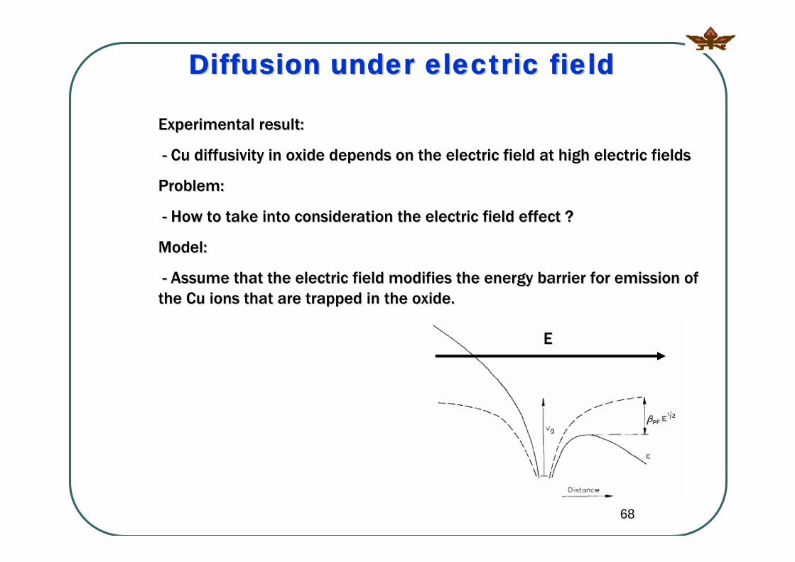
Diffusion under electric fieldDiffusion under electric field
Experimental result: Experimental result:
-- Cu diffusivity in oxide depends on the electric field at high eCu diffusivity in oxide depends on the electric field at high electric fieldslectric fields
Problem:Problem:
-- How to take into consideration the electric field effect ?How to take into consideration the electric field effect ?
Model:Model:
-- Assume that the electric field modifies the energy barrier for Assume that the electric field modifies the energy barrier for emission of emission of the Cu ions that are trapped in the oxide.the Cu ions that are trapped in the oxide.
EE

69
What affects the diffusivity at high fields ?What affects the diffusivity at high fields ?
D, Diffusivity = D, Diffusivity = λλ22 νν00 Exp[Exp[--qEqEaa/kT/kT]]
νν0 0 = lattice vibration frequency= lattice vibration frequency
EEaa = Activation energy for de= Activation energy for de--trappingtrapping
λλ= jump distance ( between trapping sites)= jump distance ( between trapping sites)
•• Ea is a function of the electric fieldEa is a function of the electric field
•• It is a local effect, hence it affects diffusivity directlyIt is a local effect, hence it affects diffusivity directly
Diffusivity definition in a 3D random Diffusivity definition in a 3D random walk model between trapswalk model between traps

70
Modifying PooleModifying Poole--FrenkelFrenkel emissionemission
φ∆φ∆−φ−== kT
qkTq
eDAeTEDB
0)(
),(
20 SiO
qEεπε
=φ∆
4.02e-3From the Deff vs.
4.50e-3From Poole- Frenkel
The slope [1/eV]0.5
20 SiO
qkTqslope
επε=
( D-diffusion coefficient, A-constant, φB-barrier height, ∆φ-barrier lowering, D0-diffusion constant, T-temperature in Kelvin, E-electric field,
k-boltzman constant, q-electron charge, ε0−permittivity in vacuum, εSiO2-dielectric constant )
E

71
Results presentation methodologyResults presentation methodology
I. TS and BTS measurements under:
low electriclow electric fieldfield.
high electric fieldhigh electric field.
II. Data of BTS results under wide range of temperatures and fields.
III. Modeling using the effective diffusion coefficient
IV. Proposing a model for Cu+ transport in the oxide.
72
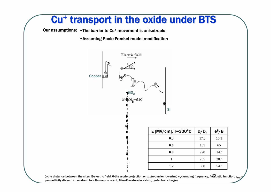
CuCu++ transport in the oxide under BTStransport in the oxide under BTS
300
265
220
165
17.5
D/D0 eB/BE [MV/cm], T=300°C
5471.2
2871
1420.8
650.6
16.10.3
(r-the distance between the sites, E-electric field, θ-the angle projection on x, ∆φ-barrier lowering, ν0- jumping frequency, f-statistic function, εsIo2−permettivity dielectric constant, k-boltzman constant, T-temperature in Kelvin, q-electron charge)
•The barrier to Cu+ movement is anisotropic
•Assuming Poole-Frenkel model modification
Our assumptionsOur assumptions::
SiOSiO22
CopperCopper
SiSi
Bfor>>)1(00)(IeDED==
The
average
effective
Di
ν∝θefdI)(000I=
The
potenti
al:
πε=4)(xVSiO
The
power:
⎢⎢⎣=kTB

73
The effective time to failureThe effective time to failure
D
xtdiff 2
2.
4α≈
Extdrift µ
β≈
0.0 0.2 0.4 0.6 0.8 1.0 1.2 1.4 1.6
4E+5
2E+5
6E+3
2E+3
8E+3
3E+3
1E+3
4E+2
1E+2
5E+1
2E+1
1E+1
0.18MV/cm, 4hr
E [MV/cm]
tf [sec]
tf(2750C)
tf-Diff.(2750C)
tf-Drift(2750C)
••The time to failure, depending on the componentsThe time to failure, depending on the components’’ diffusiondiffusion::
••The time to failure, as depending on the componentsThe time to failure, as depending on the components’’ driftdrift::
1ft≈
diftt11∝
ft1≈
ffoorr
tdiff.<<
tdrift tthh
ffoorr
tdiff.>>
tdrift tthh
••TThhee
ttiimmee
ttoo
ffaaiilluurree
iinn
tthh
3.03e-3 [1/eV]0.5
EQf eddEt
0µ=
µ=
The slope:
⎟⎟
⎠
⎞
⎜⎜
⎝
⎛−+++≈ 1
41
21111 .
.. drift
diff
diffdriftdifff tt
tttt driftdifff ttt111
.+∝⇒
74
DISCUSSIONDISCUSSIONThe capacitance techniquescapacitance techniques are more sensitive to the penetration of Cu into the oxide than current measurements.
The transient capacitance measurementhave been proven to be the most sensitive in identifying the penetration of Cu onto the Si substrate.
The I-t measurement let us know the exact time to failure and control the stress in-situ.
T e l A v i v U n i v e r s i t y

75
SummarySummaryThe major effects that indicate a coming failure are:
C-V curve:The curve distortion and a noticeable shift of the flat-band voltage.Hysteresis effectsAn increase In the inversion capacitance and a decrease in the accumulation capacitanceApart of the capacitors looses his ability to form an inversion layer so a deep depletion layer appears
C-t curve:Minority’s lifetime decreased sharply
I-V, I-t curves:The leakage currents become stronger, exceeding to values greater than 10-6A
T e l A v i v U n i v e r s i t y

76
ConclusionsConclusionsThe effectiveness of CoWP as a Barrier Layer against Cu transport was demonstrated.
In BTS under low electric field the temperature assists the Cu transport, while during BTS under high electric field the magnitude of the phenomenon determines mainly by the electric field.
The Deff of Cu under BTS was calculated and correlated under various conditions.
Cu+ transport though the oxide under BTS in a modification of the Poole-Frenkel mechanism.
T e l A v i v U n i v e r s i t y