Embed Size (px)
Citation preview
PhotomaskPhotomaskBACUS—The international technical group of SPIE dedicated to the advancement of photomask technology.
N • E • W • S
august 2019 Volume 35, Issue 8
Industry BrIefs—see page 10
CalendarFor a list of meetings —see page 11
Take A Look Inside:
Photronics Best Oral Paper
Rapid Image-Based Pupil Plane Characterization for EUV Lithography SystemsZac Levinson and Bruce W. Smith, Rochester Institute of Technology, 168 Lomb Memorial Drive, Rochester, NY 14623
Erik Verduijn, Timothy Brunner, and Obert Wood, GLOBALFOUNDRIES, 400 Stone Break Rd. Extension, Malta, NY, 12020
ABSTRACTAs the power of laser produced plasma sources has increased, EUV lens heating has become a major component of process variation. Differential lens heating can cause thermal aberrations which affect system drift during operation, therefore pupil plane characterization will play a critical role in process optimization for EUV lithography (EUVL). In-situ full pupil characteriza-tion, which depicts the pupil in its in-use state, is essential for these tools. To this end we have developed Quick Inverse Pupil (QUIP)—a software suite developed for rapid characterization of pupil plane behavior based on images formed by that system. This algorithm is based on statistical modeling, which correlates image-space variation with known aberrations. Previously we have presented variations on this algorithm which can only measure third-order aberra-tions and requires aerial image data. In this paper, we will present an approach to measure high order aberrations from images formed in resist. An inverse pupil solution will be obtained from CD-SEM image analysis. We will show that the additional degrees of freedom required to measure high-order aberrations can be achieved through using different pitches of the metrology targets. We will demonstrate that this technique can accurately determine third- and fifth-order aberrations with a retrieval error below 0.5 miliwaves in under one second. A combination of synthetic and experimental data will be presented.
1. IntroductionOver the past forty years’ lithographers have pushed Moore’s law forward by first decreasing the wavelength used in lithography systems, then by increasing the size of the lens NA (numerical aperture).1 Both of these allow lithographers to resolve smaller features, and therefore make smaller transistors. Aberrations must be sufficiently controlled for the resolution to actually increase when moving to a higher NA though.2,3 Additionally, the immense power dissipated through a lithography lens during HVM (high volume manufacturing) production has been shown to lead to thermal drift.4
In next-generation EUVL systems, measuring, and monitoring aberrations are more important than ever.3 Interferometric techniques are the de facto standard of measuring aberrations, however they do not reflect the tool in its in-use state.5–7 Less than 1% of the source energy makes it to the wafer in EUVL projection systems—the rest is dissipated as heat through the lens—therefore monitoring aberrations while in the tool is in use should be seen as critical to HVM insertion. Any aberration retrieval technique fit for HVM should also be able to measure high-order aberrations. Other techniques to measure high-order aberrations generally involve
1080
9-22
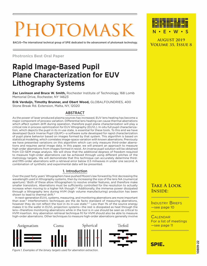
Figure 1. Examples of the binary targets used for aberration extraction.

N • E • W • S
BACUS News is published monthly by SPIE for BACUS, the international technical group of SPIE dedicated to the advancement of photomask technology.
Managing Editor/Graphics Linda DeLano
SPIE Sales Representative, Exhibitions, and Sponsorships Melissa Farlow
BACUS Technical Group Manager Marilyn Gorsuch
■ 2019 BACUS Steering Committee ■
PresidentPeter D. Buck, Mentor Graphics Corp.
Vice-PresidentEmily E. Gallagher, imec
SecretaryKent Nakagawa, Toppan Photomasks, Inc.
Newsletter EditorArtur Balasinski, Cypress Semiconductor Corp.
2019 Annual Photomask Conference ChairsJed Rankin, GLOBALFOUNDERIES Inc.
Moshe Preil, KLA-Tencor Corp.
International Chair Uwe F. W. Behringer, UBC Microelectronics
Education ChairFrank E. Abboud, Intel Corp.
Members at LargeMichael D. Archuletta, RAVE LLC
Brian Cha, Samsung Electronics Co., Ltd.Derren Dunn, IBM Corp.
Thomas B. Faure, GLOBALFOUNDRIES Inc.Aki Fujimura, DS2, Inc.
Brian J. Grenon, Grenon ConsultingJon Haines, Micron Technology Inc.
Naoya Hayashi, Dai Nippon Printing Co., Ltd.Bryan S. Kasprowicz, Photronics, Inc.
Patrick M. Martin, Applied Materials, Inc.Jan Hendrik Peters, bmbg consult
Stephen P. Renwick, Nikon Research Corp. of America
Douglas J. Resnick, Canon Nanotechnologies, Inc.Thomas Scheruebl, Carl Zeiss SMT GmbHThomas Struck, Infineon Technologies AG
Bala Thumma, Synopsys, Inc.Anthony Vacca, Automated Visual Inspection
Michael Watt, Shin-Etsu MicroSi Inc.Larry Zurbrick, Keysight Technologies, Inc.
P.O. Box 10, Bellingham, WA 98227-0010 USATel: +1 360 676 3290Fax: +1 360 647 1445
©2019
All rights reserved.
Editorial Mask Maker AppreciationTom Faure, GLOBALFOUNDRIES CorporationHistorically, many chip makers have treated masks at the mature technology nodes as a readily available and cheap commodity, but recently the tables have turned. The value of this commodity has increased due to huge demand in more mature nodes, thanks to the Internet of Things as well as increased demand on the high end nodes due to heavy use of multi-patterning. Many forget the famous semiconductor industry inverted pyramid revenue chart which shows mask makers near the bottom of the pyramid, but a key neces-sity for enabling the semiconductor and electronics industries. Recent data published by SEMI in May (see ‘Renaissance in the Photomask Market ?’) shows that mask making revenue grew by 13 percent and 8 percent in 2017 and 2018 respectively, and the total worldwide photomask revenue in 2018 reached a record high of $4 billion. This is further supported by data from the 2018 E-beam Initiative Mask maker survey which shows that the 10 mask makers participating in the survey shipped 27% more masks in 2018 versus 2017. The biggest increases in shipments occurred in the more mature 65 nm and older tech nodes.
These strong increases in demand have caused mask makers to struggle to meet the higher volumes of masks being requested at the more mature nodes. But, the mask makers can’t simply add capacity because they are unable to buy new copies of the original capital equipment used to make these masks, as Franklin Kalk mentioned in his 2018 ebeam initiative talk titled ‘Renew, Retire, Replace: How the mask equipment industry can transmform its products and become healthy again’. For example, low cost i-line laser writers are no longer available to purchase. In addition low cost 488 nm and 365 nm die to die and die to database patterned mask defect inspection tools are no longer being manufactured. This high demand and inability to purchase ‘copy exact’ new equipment has created a thriving market for used mask making equipment, and prices of used equipment have increased dramatically. However, there is still not enough used equipment to keep up with the industry needs.
This makes securing high quality and timely mask supply in such environ-ment of very high mask demand in the mature nodes a challenge for chip makers. They will need to give in on price as the number one determiner of which merchant mask maker gets their business. They would be wise to establish more truly collaborative relationships and treat their mask sup-pliers as partners instead of a supplier of a low tech commodity that can be sourced from other merchant masks shops. As part of this collaborative relationship, chip makers will need to be more flexible and work with mask makers to qualify new/different mask writers and inspection equipment for use in building masks for the mature nodes to help increase mask fabrica-tion options and capacity. In some cases, this may require updates to OPC models due to a significant change in mask writer (for example from laser to ebeam). Failure to be more flexible and collaborative with mask makers at the mature nodes will leave chip makers at risk being shut out during periods of high mask demand.
This new demand dynamic and aging/obsolescence of the mask making equipment used for manufacturing masks at the mature node only improves the case for chip makers to show increased appreciation of their mask mak-ers. Mask makers continue to bail out chip makers in the form of rapid TAT on emergency re-designs, last minute OPC fixes, and numerous re-pells. So, chip makers, I would encourage you to take the time to show some appre-ciation to your mask makers and treat them with the respect they deserve. They are more valuable than ever.

using different types of illumination (eg. ARTEMIS, TAMIS), but this is not desired for EUVL due to the decrease in wafer throughput and increase in production costs.8–10
In previous reports we have demonstrated techniques to extract the aberrations of EUV imaging systems both from wafer CD measurements and from aerial images.11–13 These mea-surements were of purely low-order aberrations and lumped the effects of high-order terms into one single effective term. In this paper we show a CD-based technique for measuring both low- and high-order aberrations. This technique is based on previous work using eigenfunctions derived from principal component analysis. Using this technique, combined with pre-built models, aberrations can be extracted in under one second.
2. Background
2.1 A naïve exampleThe goal of this work is to measure both the low- and high-order aberrations of an imaging system from images formed by that system. To that end, we will first consider the effects of these terms in the wafer plane. Consider an imaging system in the coherent limit with a 1D slit pupil with a pupil function given by,
(1)
A line-space array with pitch P will be imaged in the wafer plane as,
(2)
where p1 is defined to be the spatial frequency, or 1/P. Suppose the pupil function is given by an ideal top-hat transmission with some combination of, for example, third-order and fifth-order coma aberration. This can be given as,
(3)
where A is the amount of third-order coma, and B is the amount of fifth-order coma. Coma is an odd-parity aberration, therefore the pupil function has the property,
(4)
Figure 2. Examples of a ΔCD eigenfunction (left) and the projection curve (right) for (a) astigmatism, (b) coma, (c) spherical aberration, and (d) trefoil. Astigmatism is interrogated by the CD difference between orthogonal lines and spaces. Coma is interrogated by the CD difference between the outer two bars of a five bar structure. Spherical is interrogated by a heuristic computed from a constant CD line at pitches 1:1, 1:2, and 1:4. Trefoil is interrogated by the CD difference between orthogonal lines and spaces.
Volume 35, Issue 8 Page 3
N • E • W • S

and in this specific case,
(5)
The image can then be given by,(6)
Both sinusoidal terms have the same phase shift given by W(p1). The spatial frequency p1 is known and we can measure the aerial image I(x). The phase shift can be fit to an experimental aerial image with, for example, non-linear least squares. Therefore, the value of the pupil function at p1 can be determined experimen-tally from the aerial image. However, the amount of third-order coma can be written as,
(7)
Therefore, there are multiple combinations of A and B that can lead to the same aberrated aerial image. Measuring the image at one pitch is not sufficient to determine both low and high order aberrations. A single binary target that can measure both low and high order aberrations from the same image does not exist because there is not enough information in the image. If we also measure the image at another pitch with spatial frequency p2 then we have an equation analogous to Equation (7), but with p2 instead of p1. Combining and simplifying we find that the amount of fifth-order coma can be given as,
(8)If instead the pupil function were even-parity it would have the property,
(9)
Equation (6) therefore becomes,
(10)
The sinusoidal term involving the pupil function acts as a phase shift and can also be experimentally determined from an aerial image. Therefore, for either even- or odd-parity aberrations, if we have images from two different pitches we can determine both the low- and high-order aberrations from experimentally measured quantities.
This example serves two purposes: 1) to illustrate the most basic form of the inverse problem we are solving, and 2) to show that there is not enough information in a single image to measure high-order aberrations. In practice aberrations are not correlated with sinusoidal phase shifts to measure aberrations in lithography systems. This is because lithographers gener-ally cannot directly measure the aerial image and because this method could be extremely sensitive to noise. All aberration measurements do correlate an image-domain quantity with aberrations though.
2.2 ΔCD EigenfunctionsIn previous reports we have shown an iterative algorithm to measure pupil variation from wafer CD measurements.11,14 This technique uses the targets show in Figure 1. CDs are measured at the locations marked by the red line, then a ΔCD function is computed either through focus (for even-parity aberrations) or through dose (for odd-parity aberrations). This ΔCD function is correlated with the amount of aberration, and a full inverse pupil solution is obtained through iteration. This technique has the disadvantage that aerial image simulations occur within the iterative loop. Simulations are therefore run redundantly which in turn causes a significant reduction in turnaround time.
We have also previously shown that aberrations can be measured by projecting an aberrated aerial image onto an eigenfunction and correlating the projection coefficient with the amount of aberration.13 These eigenfunctions are specific to the set of metrology targets and the imaging system and describe the action of each aberration in the image domain We have shown that the eigenfunctions can be computed either
Figure 3. Comatic eigenfunction with varying amounts of trefoil. There are five lines plotted, despite only three being visible. This is because two are on top of each other because the eigenfunction is even in the Z10 axis.
Page 4 Volume 35, Issue 8
N • E • W • S
directly from eigenvector decomposition of the TCC (trans-mission cross coefficient) function, similar to SOCS (sum of coherent systems) decomposition, or by principal component analysis (PCA). One could calculate the eigenfunctions using either method and obtain identical eigenfunctions.
It is advantageous to consider the CD analogue to aerial image aberration eigenfunctions because the aerial image is difficult to measure directly from a production scanner. While it is always possible to compute aerial images from a TCC, it is not possible in general to analytically find CDs from an aerial image. For the simplest of cases an analytic CD function may be possible, but in practice root-finding algorithms are the saf-est approach. This property means that while the aerial image aberration eigenfunctions could be computed directly, there is no such CD eigenfunction that can be computed directly from either the aerial image or aerial image eigenfunction.
Because we cannot analytically compute a ΔCD function from the TCC, we must instead use PCA to compute the ei-genfunctions. Examples of the resulting eigenfunctions and the projection curves are given in Figure 2 for astigmatism, coma, spherical aberration, and trefoil. To compute these the ΔCD function is computed as in Figure 1, then PCA is used to find the eigenfunction representing the variation due to aber-rations. The projection of ΔCD functions onto their respective eigenfunctions is also shown. Each of the curves is invertible into a single-valued function and can therefore be used to measure aberrations from experimental CD measurements. It is notable that the projection curve for spherical aberration appears to be approaching an extremum in the negative aberration direction. It is possible that degeneracy may exist for aberrations greater than 0.1 ml, but this is above the aberration levels of state of the art EUVL scanners.
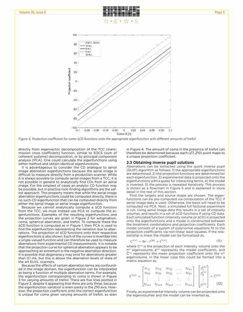
Because the effects of certain aberration terms are confound-ed in the image domain, the eigenfunction can be interpreted as being a function of multiple aberration terms. For example, the eigenfunction corresponding to coma is shown in Figure 3 for varying amounts of trefoil. There are five lines plotted in Figure 3, despite it appearing that there are only three, because the eigenfunction variation is even-parity in the Z10 axis. How-ever, the projection coefficient onto the correct eigenfunction is unique for coma given varying amounts of trefoil, as seen
in Figure 4. The amount of coma in the presence of trefoil can therefore be determined because each (Z7, Z10) point maps to a unique projection coefficient.
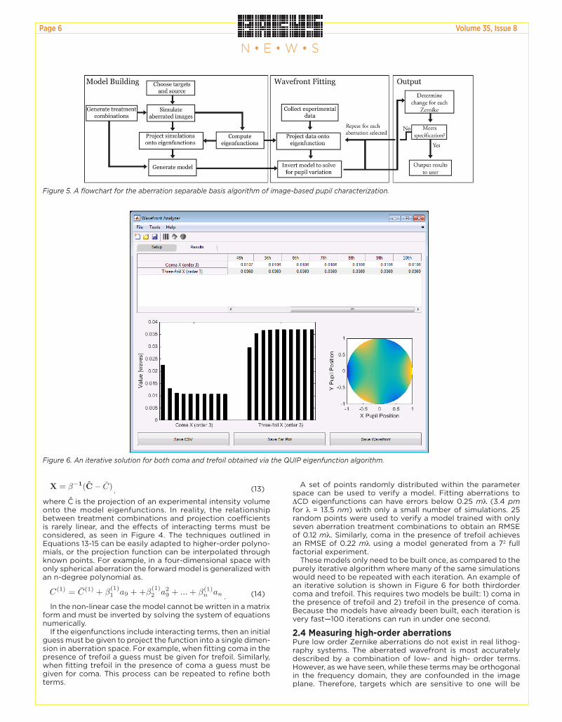
2.3 Obtaining inverse pupil solutionsAberrations can be extracted using the quick inverse pupil (QUIP) algorithm as follows: 1) the appropriate eigenfunctions are determined, 2) the projection functions are determined for each eigenfunction, 3) experimental data is projected onto the eigenfunctions with a guess for interacting terms, 4) the model is inverted, 5) the process is repeated iteratively. This process is shown as a flowchart in Figure 5 and is explained in more detail in the rest of this section.
First the targets and source shape are chosen. The eigen-functions can be pre-computed via computation of the TCC if aerial image data is used. Otherwise, the basis will need to be computed via PCA. Next, a simulated full factorial experiment is run. Using aerial image data this results in a set of intensity volumes, and results in a set of ΔCD functions if using CD data. Each simulated function (intensity volume or ΔCD) is projected onto the eigenfunctions and a model is constructed between the treatment combinations and projection coefficients. Each model consists of a system of polynomial equations fit to the projection coefficients via non-linear least squares. If the rela-tionship is linear the model can be formalized as,
(11)
where C(n) is the projection of each intensity volume onto the nth eigenvolume, b(n) represents the model coefficients, and C-(n) represents the mean projection coefficient onto the nth eigenvolume. In the linear case this could be formed into a matrix equation as.
(12)
Finally, an experimental intensity volume can be projected onto the eigenvolumes and the model can be inverted as,
Figure 4. Projection coefficient for coma ΔCD functions onto the appropriate eigenfunction with different amounts of trefoil.
Volume 35, Issue 8 Page 5
N • E • W • S
(13)
where C ˆ is the projection of an experimental intensity volume onto the model eigenfunctions. In reality, the relationship between treatment combinations and projection coefficients is rarely linear, and the effects of interacting terms must be considered, as seen in Figure 4. The techniques outlined in Equations 13-15 can be easily adapted to higher-order polyno-mials, or the projection function can be interpolated through known points. For example, in a four-dimensional space with only spherical aberration the forward model is generalized with an n-degree polynomial as.
(14)
In the non-linear case the model cannot be written in a matrix form and must be inverted by solving the system of equations numerically.
If the eigenfunctions include interacting terms, then an initial guess must be given to project the function into a single dimen-sion in aberration space. For example, when fitting coma in the presence of trefoil a guess must be given for trefoil. Similarly, when fitting trefoil in the presence of coma a guess must be given for coma. This process can be repeated to refine both terms.
A set of points randomly distributed within the parameter space can be used to verify a model. Fitting aberrations to ΔCD eigenfunctions can have errors below 0.25 ml (3.4 pm for l = 13.5 nm) with only a small number of simulations. 25 random points were used to verify a model trained with only seven aberration treatment combinations to obtain an RMSE of 0.12 ml. Similarly, coma in the presence of trefoil achieves an RMSE of 0.22 ml using a model generated from a 72 full factorial experiment.
These models only need to be built once, as compared to the purely iterative algorithm where many of the same simulations would need to be repeated with each iteration. An example of an iterative solution is shown in Figure 6 for both thirdorder coma and trefoil. This requires two models be built: 1) coma in the presence of trefoil and 2) trefoil in the presence of coma. Because the models have already been built, each iteration is very fast—100 iterations can run in under one second.
2.4 Measuring high-order aberrationsPure low order Zernike aberrations do not exist in real lithog-raphy systems. The aberrated wavefront is most accurately described by a combination of low- and high- order terms. However, as we have seen, while these terms may be orthogonal in the frequency domain, they are confounded in the image plane. Therefore, targets which are sensitive to one will be
Figure 6. An iterative solution for both coma and trefoil obtained via the QUIP eigenfunction algorithm.
Figure 5. A flowchart for the aberration separable basis algorithm of image-based pupil characterization.
Page 6 Volume 35, Issue 8
N • E • W • S
sensitive to the other. This problem is similar to differentiating coma from trefoil.
While trefoil is not a high-order comatic term, patterns that are sensitive to coma will be sensitive to trefoil and vice-versa. Therefore, measuring high-order terms can be approached simi-larly to measuring coma and trefoil together. The models must include all confounded terms and must be solved iteratively.
In addition, high-order terms require the use of multiple pitches of the same type of target. This gives enough informa-tion to distinguish between low- and high-order terms in the image domain. Using the QUIP algorithm, high-order terms are fit by creating a model for the low-order term in the presence of the high-order term, and vice versa. Then the algorithm proceeds as above for coma and trefoil.
Any algorithm that measures high-order aberrations must perform accurately under three types of situations: a wavefront composed from only third-order aberrations, one composed from only fifth-order aberrations, and one composed from a mixture of both third- and fifth-order aberrations. These three test cases assure that the algorithm is not changing the low-order terms and is correctly fitting the high-order terms.
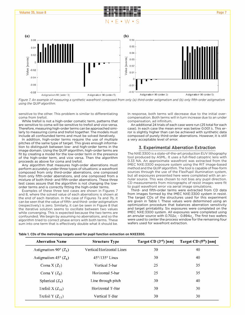
Examples of these three test cases are shown in Figures 7 and 8, where the solved value of each aberrations is shown at the end of each iteration. In the case of Figures 7a and 7b, it can be seen that the value of fifth- and third- order astigmatism (respectively) is zero. Similarly, it can be seen in Figure 8 that the iterative solution seems to oscillate between two values while converging. This is expected because the two terms are confounded. We begin by assuming no aberrations, and so the algorithm tried to correct phase errors with both terms. These sum into one term that is effectively double what it should be.
In response, both terms will decrease due to the initial over-compensation. Both terms will in turn increase due to an under compensation, ad infinitum.
An additional 24 trials of each case were run (25 total for each case). In each case the mean error was below 0.001 l. This er-ror is slightly higher than can be achieved with synthetic data composed of purely third-order aberrations. However, it is still a very acceptable level of error.
3. Experimental Aberration ExtractionThe NXE:3300 is a state-of-the-art production EUV lithography tool produced by ASML. It uses a full-filed catoptric lens with 0.33 NA. An approximate wavefront was extracted from the IMEC NXE:3300 exposure system using the RIT image-based method and the QUIP algorithm. The tool is capable of free-form sources through the use of the FlexPupil illumination system, but all exposures presented here were completed with an an-nular source. This was chosen to not bias any pupil direction. CD measurements from micrographs of resist images were fit to pupil wavefront error via aerial image simulations.
Third- and fifth-order terms were extracted from CD data from images formed by the IMEC NXE:3300 system in resist. The target CDs of the structures used for this experiment are given in Table 1. These values were determined using an optimization procedure that balances aberration sensitivity and target printability. Six exposures were completed on the IMEC NXE:3300 system. All exposures were completed using an annular source with 0.702σi – 0.894σo. The first two wafers were used to center the process window for the remaining four wafers used for wavefront extraction.
Figure 7. An example of measuring a synthetic wavefront composed from only (a) third-order astigmatism and (b) only fifth-order astigmatism using the QUIP algorithm.
Table 1. CDs of the metrology targets used for pupil function extraction on NXE3300.
Volume 35, Issue 8 Page 7
N • E • W • S
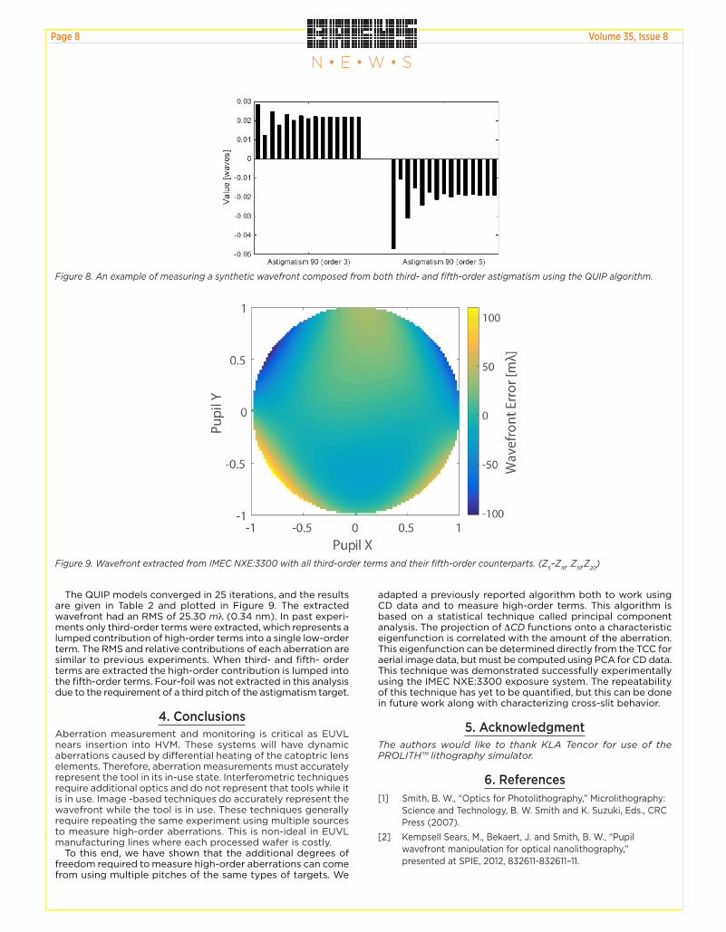
The QUIP models converged in 25 iterations, and the results are given in Table 2 and plotted in Figure 9. The extracted wavefront had an RMS of 25.30 ml (0.34 nm). In past experi-ments only third-order terms were extracted, which represents a lumped contribution of high-order terms into a single low-order term. The RMS and relative contributions of each aberration are similar to previous experiments. When third- and fifth- order terms are extracted the high-order contribution is lumped into the fifth-order terms. Four-foil was not extracted in this analysis due to the requirement of a third pitch of the astigmatism target.
4. ConclusionsAberration measurement and monitoring is critical as EUVL nears insertion into HVM. These systems will have dynamic aberrations caused by differential heating of the catoptric lens elements. Therefore, aberration measurements must accurately represent the tool in its in-use state. Interferometric techniques require additional optics and do not represent that tools while it is in use. Image -based techniques do accurately represent the wavefront while the tool is in use. These techniques generally require repeating the same experiment using multiple sources to measure high-order aberrations. This is non-ideal in EUVL manufacturing lines where each processed wafer is costly.
To this end, we have shown that the additional degrees of freedom required to measure high-order aberrations can come from using multiple pitches of the same types of targets. We
adapted a previously reported algorithm both to work using CD data and to measure high-order terms. This algorithm is based on a statistical technique called principal component analysis. The projection of ΔCD functions onto a characteristic eigenfunction is correlated with the amount of the aberration. This eigenfunction can be determined directly from the TCC for aerial image data, but must be computed using PCA for CD data. This technique was demonstrated successfully experimentally using the IMEC NXE:3300 exposure system. The repeatability of this technique has yet to be quantified, but this can be done in future work along with characterizing cross-slit behavior.
5. Acknowledgment The authors would like to thank KLA Tencor for use of the PROLITH™ lithography simulator.
6. References[1] Smith, B. W., “Optics for Photolithography,” Microlithography:
Science and Technology, B. W. Smith and K. Suzuki, Eds., CRC Press (2007).
[2] Kempsell Sears, M., Bekaert, J. and Smith, B. W., “Pupil wavefront manipulation for optical nanolithography,” presented at SPIE, 2012, 832611-832611–11.
Figure 8. An example of measuring a synthetic wavefront composed from both third- and fifth-order astigmatism using the QUIP algorithm.
Figure 9. Wavefront extracted from IMEC NXE:3300 with all third-order terms and their fifth-order counterparts. (Z5–Z16, Z19,Z20)
Page 8 Volume 35, Issue 8
N • E • W • S

[3] Krautschik, C. G., Ito, M., Nishiyama, I. and Mori, T., “Quantifying EUV imaging tolerances for the 70-, 50-, 35-nm modes through rigorous aerial image simulations,” presented at SPIE, 2001, 524–534.
[4] Martin, C. J., Engelstad, R. L. and Lovell, E. G., “Thermomechanical modeling of the EUV reticle during exposure,” presented at SPIE, 2001, 515–523.
[5] Foucault, L., “Description des procedees employes pour reconnaitre la configuration des surfaces optiques,” C. R. Acad. Sci. 47(47), 958ff (1858).
[6] Linnik, W. P., “A simple interferometer for the investigation of optical systems,” Proc. Academy of Sci of the USSR 1, 208 (1933).
[7] Naulleau, P. P., Goldberg, K. A. and Bokor, J., “Extreme ultraviolet carrier-frequency shearing interferometry of a lithographic four-mirror optical system,” Journal of Vacuum Science & Technology B 18(6), 2939–2943 (2000).
[8] Dirksen, P., Juffermans, C. A., Engelen, A., De Bisschop, P. and Muellerke, H., “Impact of high-order aberrations on the performance of the aberration monitor,” Microlithography 2000, 9–17 (2000).
[9] Dirksen, P., Juffermans, C. A., Pellens, R. J., Maenhoudt, M. and De Bisschop, P., “Novel aberration monitor for optical lithography,” Microlithography’99, 77–86 (1999).
[10] van de Kerkhof, M. A., de Boeij, W., Kok, H., Silova, M., Baselmans, J. and Hemerik, M., “Full optical column characterization of DUV lithographic projection tools,” presented at SPIE, 2004, 1960–1970.
[11] Fenger, G., “Image-based EUVL Aberration Metrology,” Thesis, Rochester Institute of Technology (2013).
[12] Levinson, Z., Verduijn, E., Wood, O. R., Mangat, P., Goldberg, K. A., Benk, B., Markus P., Wojdyla, A. and Smith, B. W., “Measurement of EUVL Pupil Amplitude and Phase Variation via Image-Based Methodology,” J. Micro Nanolith. MEMS MOEMS (2016).
[13] Levinson, Z., Burbine, A., Verduijn, E., Wood, O., Goldberg, K. A., Benk, M. P., Wojdyla, A. and Smith, B. W., “Image-based pupil plane characterization via a space-domain basis,” J. Micro/Nanolith. MEMS MOEMS 16(2), 023509–023509 (2017).
[14] Levinson, Z., Fenger, G., Burbine, A., Schepis, A. R. and Smith, B. W., “Optimization of image-based aberration metrology for EUV lithography,” presented at SPIE, 17 April 2014, 90482M.
Table 2. Extracted Zernike aberrations for each aberration type for the IMEC NXE:3300.
Volume 35, Issue 8 Page 9
N • E • W • S

N • E • W • S
Sponsorship OpportunitiesSign up now for the best sponsorship
opportunities
Photomask Technology + EUV Lithography 2019 Contact: Melissa Farlow,
Tel: +1 360 685 5596; [email protected]
Advanced Lithography 2020Contact: Teresa Roles-Meier,
Tel: +1 360 685 5445; [email protected]
Advertise in the BACUS News!
The BACUS Newsletter is the premier publication serving the photomask industry. For information on how to advertise, contact:
Melissa Farlow, Tel: +1 360 685 5596 [email protected]
BACUS Corporate Members
Acuphase Inc.American Coating Technologies LLCAMETEK Precitech, Inc.Berliner Glas KGaA Herbert Kubatz
GmbH & Co.FUJIFILM Electronic Materials U.S.A., Inc.Gudeng Precision Industrial Co., Ltd.Halocarbon ProductsHamaTech APE GmbH & Co. KGHitachi High Technologies America, Inc.JEOL USA Inc.Mentor Graphics Corp.Molecular Imprints, Inc.Panavision Federal Systems, LLCProfilocolore SrlRaytheon ELCAN Optical TechnologiesXYALIS
■ Semicon West Sluggish with Hopes of 2020 Recovery
The semiconductor industry is cyclical, and it appears to be entering a mild down cycle. Companies are still profitable and in relatively good shape despite extended holiday shutdowns. The recovery is likely to balance memory and logic, include an emphasis on EUV as it enters manufacturing and probably shift away from US suppliers towards China. https://semiwiki.com/semiconductor-services/semiconductor-advisors/273576-semicon-west-was-sluggish-with-hopes-of-2020-recovery/
■ Huawei Ban Could Come Back to Bite U.S.
The short-term impact of cutting Huawei’s supply of US chips and components will be severe. Longer-term, the ban will likely encourage China to become self-reliant. The Chinese government already supports its domestic semiconductor production and is planning to invest over $160 billion in the next 10 years. In five years, China could be completely independent of US chips as long as it can order from the major foundries TSMC and Samsung. https://www.eetimes.com/document.asp?doc_id=1334795
■ Japan: ASML and Mitsui Chemicals Sign License Agreement for EUV Pellicle Business
ASML developed EUV pellicles for commercial use in its EUV lithography systems. Mitsui Chemicals concluded a license agreement for this EUV pellicle business with ASML. The license agreement will add EUV capability to the business Mitsui launched in 1984. Mitsui Chemicals will build an EUV pellicle assembly factory at Iwakuni Otake Works. Sales of EUV pellicle to customers is anticipated in 2021. https://www.marketwatch.com/press-release/japan-asml-and-mitsui-chemicals-sign-license-agreement-for-euv-pellicle-business-2019-05-31
■ Debate Over Health Of Moore’s Law Continues
Support for Moore’s law continues at Semicon West, though a slower pace is acknowledged. Some perspectives are slightly different now. The technical and cost challenges of scaling persist. Cost matters, and can slow the rate of technology introduction, but the application domain is expanding. For example, machine learning and other data analytics are based on faster computation, more memory, and more data. This will lead to vertical packaging – consolidating more capability into one chip. https://semiengineering.com/debate-over-health-of-moores-law-continues/
■ ASML on the Up Despite Wider Semi Slowdown
While there is an expected drop in the semiconductor equipment market this year, ASML is executing an “up” year for its sales. Second quarter earnings were very strong, and the second half will be as well based on bookings. While memory volumes may be down, there is a continued strong demand for logic using EUV scanners. http://optics.org/news/10/7/29
■ 200mm Cools Off, But Not For Long
200mm fabs are older facilities with more mature processes and they produce a tremendous volume of critical chips: analog, MEMS, RF and others. From 2016 to 2018 there were shortages of both 200mm fab capacity and equipment in the market. In 2019. Demand slowed with the IC industry, but in the future the demand will recover and 200mm capacity will again be limited. 200mm is not leading edge processing, but is good business and some critical investments are needed. https://semiengineering.com/200mm-cools-off-but-not-for-long/
Page 10 Volume 35, Issue 8
N • E • W • S
Industry Briefs

SPIE is the international society for optics and photonics, an educational not-for-profit organization founded in 1955 to advance light-based science, engineering, and technology. The Society serves nearly 264,000 constituents from 166 countries, offering conferences and their published proceedings, continuing education, books, journals, and the SPIE Digital Library in support of interdisciplinary information exchange, professional networking, and patent precedent. SPIE provided more than $4 million in support of education and outreach programs in 2018. spie.org
International HeadquartersP.O. Box 10, Bellingham, WA 98227-0010 USA Tel: +1 360 676 3290 Fax: +1 360 647 [email protected] • spie.org
Shipping Address1000 20th St., Bellingham, WA 98225-6705 USA
Managed by SPIE Europe 2 Alexandra Gate, Ffordd Pengam, Cardiff, CF24 2SA, UK Tel: +44 29 2089 4747 Fax: +44 29 2089 [email protected] • spieeurope.org
2019SPIE Photomask Technology + EUV Lithography 15-19 September 2019Monterey Conference Center and Monterey MarriottMonterey, California, USAwww.spie.org/puv
2020SPIE Advanced Lithography23-27 February 2020 San Jose Marriott and San Jose Convention Center San Jose, California, USA
Photomask JapanApril 2020Japan
The 36th European Mask and Lithography Conference, EMLC 2020June 2020Germany
Corporate Membership Benefits include:■ 3-10 Voting Members in the SPIE General Membership,
depending on tier level
■ Subscription to BACUS News (monthly)
■ One online SPIE Journal Subscription
■ Listed as a Corporate Member in the BACUS Monthly Newsletter spie.org/bacushome
C A L E N D A R
About the BACUS GroupFounded in 1980 by a group of chrome blank users wanting a single voice to interact with suppliers, BACUS has grown to become the largest and most widely known forum for the exchange of technical information of interest to photomask and reticle makers. BACUS joined SPIE in January of 1991 to expand the exchange of information with mask makers around the world.
The group sponsors an informative monthly meeting and newsletter, BACUS News. The BACUS annual Photomask Technology Symposium covers photomask technology, photomask processes, lithography, materials and resists, phase shift masks, inspection and repair, metrology, and quality and manufacturing management.
Individual Membership Benefits include:■ Subscription to BACUS News (monthly)■ Eligibility to hold office on BACUS Steering Committee
spie.org/bacushome
You are invited to submit events of interest for this calendar. Please send to [email protected].
h
h
Join the premier professional organization for mask makers and mask users!
h
h
Volume 35, Issue 8 Page 11
N • E • W • S