Embed Size (px)
Citation preview

PEB-6630/6631VLA
Embedded System Board
User's Manual
P/N: AB1-103/AB1-104 Version 1.0
Copyright © Portwell, Inc., 2002. All rights reserved. All other brand names are registered trademarks of their respective owners.

Table of Contents
How to Use This Manual CHAPTER 1 Introduction..................................................................................................... 1-1
1.1 Check List ................................................................................................................... 1-2 1.2 Product Specifications .............................................................................................. 1-3 1.3 System Architecture.................................................................................................. 1-6
CHAPTER 2 Hardware Configuration Setting ................................................................ 2-1
2.1 Jumpers Position and Setting Table ....................................................................... 2-2 2.2 Connectors ................................................................................................................. 2-3
CHAPTER 3 System Installation ........................................................................................ 3-1
3.1 Low Voltage Intel Celeron/Pentium-III Processor ............................................. 3-1 3.2 Main Memory ............................................................................................................ 3-1 3.3 Installing the Single Board Computer ................................................................... 3-2
3.3.1 INF Chipset Component Driver .................................................................. 3-2 3.3.2 Intel 82815 GMCH Graphics Controller..................................................... 3-3 3.3.3 Intel 82801BA MAC Fast Ethernet Controller ........................................... 3-4 3.3.4 Intel 82801BA AC’97 Codec Controller ...................................................... 3-4
3.4 Clear CMOS Operation............................................................................................ 3-5 3.5 Watch Dog Timer Programming............................................................................ 3-5
CHAPTER 4 BIOS Setup Information............................................................................... 4-1
4.1 Entering Setup ........................................................................................................... 4-1 4.2 Main Menu................................................................................................................. 4-3 4.3 Standard CMOS Setup Menu.................................................................................. 4-4 4.4 IDE Adaptors Setup Menu ...................................................................................... 4-6 4.5 Advanced BIOS Features ......................................................................................... 4-8 4.6 Advanced Chipset Features .................................................................................. 4-11 4.7 Integrated Peripherals............................................................................................ 4-14 4.8 Onboard FDC Controller ....................................................................................... 4-16 4.9 Onboard Serial Port 1/Port 2 ................................................................................ 4-16 4.10 UART Mode Select................................................................................................ 4-17 4.11 Power Management Setup .................................................................................. 4-19 4.12 PnP/PCI Configuration Setup............................................................................ 4-23 4.13 PC Health Status ................................................................................................... 4-25 4.14 Frequency/Voltage Control ................................................................................ 4-25 4.15 Default Menu......................................................................................................... 4-26 4.16 Supervisor/User Password Setting ................................................................... 4-27 4.17 Exiting Selecting.................................................................................................... 4-28 4.18 POST Messages ..................................................................................................... 4-28 4.19 BIOS POST Check Point List ............................................................................... 4-34 4.20 Flash BIOS Utility.................................................................................................. 4-40

CHAPTER 5 Troubleshooting ............................................................................................. 5-1 5.1 Backplane Setup ........................................................................................................ 5-1 5.2 Onboard hardware installation .............................................................................. 5-5 5.3 BIOS Setting ............................................................................................................... 5-6 5.4 OS Diagnostics........................................................................................................... 5-8

How to Use This Manual The manual describes how to configure your PEB-6630/6631VLA system to meet various operating requirements. It is divided into four chapters, with each chapter addressing a basic concept and operation of Embedded Board Computer. Chapter 1: Introduction. This chapter presents what you have in the inside of box and give you an overview of the product specifications and basic system architecture for this model of single board computer. Chapter 2: Hardware Configuration Setting. This chapter shows the definitions and locations of Jumpers and Connectors that you can easily configure your system Chapter 3: System Installation. This chapter describes how to properly mount the CPU and main memory, M-system Flash disk, or optional flat panel display interface module to get a safe installation and give you a programming guide of Watch Dog Timer function. Besides, it will introduce and show you the driver installation procedure about Graphics Controller. Chapter 4: BIOS Setup Information. This chapter specifies the meaning of each setup parameters and how to get advanced BIOS performance and update new BIOS. In addition, POST checkpoint list will give you a guide of trouble-shooting. The content of this manual and EC declaration document is subject to change without prior notice. These changes will be incorporated in new editions of the document. Portwell may make supplement or change in the products described in this document at any time. Updates to this manual, technical clarification, and answers to frequently asked questions will be shown on the following web site: http://www.portwell.com.tw

EC Declaration of Conformity
(To Be Added) For the following equipment: Product Name: Model Name: Trade Name: is herewith confirmed to comply with the requirements set out in the Council Directive on the Approximation of the Laws of the Member States relating to Electromagnetic Compatibility Directive (89/336/EEC). The equipment was evaluated and passed the test, the following standards were applied : EMC : EN 55022 (1994/A1:1995 Class A)
EN 50082-2 (1991) EN 61000-4-2 (1995)
EN 61000-4-3 (1996) EN 61000-4-4 (1995)
EN 61000-3-2 (1995) EN 61000-3-3 (1995) The following manufacturer is responsible for this declaration : Portwell, Inc. (Company Name) 3F, No.88, Sec. 1, Nei-Hu Rd., Taipei, Taiwan, R.O.C. (Company Address) Taipei, R.O.C.
Place Date Legal Signature of Authorized Person

Introduction
PEB-6630/6631VLA User’s Manual 1-1
CHAPTER 1 Introduction The PEB-6630VLA and PEB-6631VLA all-in-one half size single board computer is designed to fit a low power consumption Celeron/Pentium-III based CPU and compatible for high-end computer system with PCI Local Bus architecture. It is made to meet today’s demanding pace, and keep complete compatibility with hardware and software designed for the IBM PC/AT. It's beneficial to build up a low power system for VARs, or system integrators. The on-board 3D Graphics display, fast Ethernet interface and AC’97 controller will bring full functionality and high performance to all segments of the PC market. This single board computer runs with Intel Low Voltage Celeron (PEB-6630VLA) and Low Voltage Pentium-III (PEB-6631VLA) processor, and support one DIMM up to 512 MB SDRAM. The enhanced on-board PCI IDE interface support2 drives up to PIO mode 4 timing and Ultra DMA/33/66/100 synchronous mode feature. The on-board Super I/O Chipset integrates one floppy controller, two serial ports (one RS-232 and one RS-485), one keyboard controller, one hardware monitor, one IrDA port and one parallel port. Two high performance 16C550-compatible UARTs provide 16-byte transmit/receive FIFOs, and the multi-mode parallel port supports SPP/EPP/ECP function. Besides, one USB (Universal Serial Bus) ports provide high-speed data communication between peripherals and PC. PEB-6630/6631VLA works with multi-slots PCI-bus backplane. The Watch-Dog Timer function monitors your system status. One 6-pin Mini-DIN connector (with Y-Cable) is to connect PS/2 Mouse and Keyboard. The on-board Flash ROM makes the BIOS update easier. A standard 5-1/4” drive power connector directly gets more power energy for large power applications or used for stand-alone operation, and the additional 5-pin shrouded header connects the keyboard interface on the backplane. The high precision Real Time Clock/calendar supports Y2K for accurate scheduling and stores date information. One 4-pin header is designed to support ATX power function. All of these features make PEB-6630/6631VLA excellent in stand-alone applications.
Introduction
PEB-6630/6631VLA User’s Manual 1-2
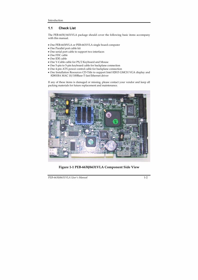
1.1 Check List The PEB-6630/6631VLA package should cover the following basic items accompany with this manual. • One PEB-6630VLA or PEB-6631VLA single board computer • One Parallel port cable kit • One serial port cable to support two interfaces • One FDC cable • One IDE cable • One Y-Cable cable for PS/2 Keyboard and Mouse • One 5-pin to 5-pin keyboard cable for backplane connection • One 4-pin ATX power control cable for backplane connection • One Installation Resources CD-Title to support Intel 82815 GMCH VGA display and
82801BA MAC 10/100Base-T fast Ethernet driver If any of these items is damaged or missing, please contact your vendor and keep all packing materials for future replacement and maintenance.
Figure 1-1 PEB-6630/6631VLA Component Side View

Introduction
PEB-6630/6631VLA User’s Manual 1-3
1.2 Product Specifications • Main processor
Intel Low Voltage Celeron or Pentium-III processors - Intel Low Voltage Celeron 400Mhz (PEB-6630VLA) - Intel Low Voltage Pentium III 700Mhz (PEB-6631VLA) - CPU bus frequency: 100 MHz - BGA2 CPU
• BIOS
Phoenix (Award) system BIOS with 4MB Firmware Hub to support DMI, PnP, APM, and ACPI
• Main Memory
One 168-pin DIMM sockets, supporting PC133/PC100 SDRAM up to 512MB (No ECC and Registered DIMM Support)
• L2 Cache Memory
128KB L2 Cache built in Celeron and 256KB in Pentium-III processor • Chipset
Intel 815E Chipset • Bus Interface
Follow PCI 2.1 standard (32-bit PCI) Fully complies with PCI Local Bus specification V2.1 (support 4 master PCI slots)
• PCI IDE Interface
Support one enhanced IDE ports up to two HDD devices with PIO mode 4 and Ultra DMA/33/66/100 mode transfer and Bus Master feature
• CF Socket Interface
Support one enhanced IDE interface to one CF socket for CF flash disk device • Floppy Drive Interface
Support one FDD port up to two floppy drives and 5-1/4"(360K, 1.2MB), 3-1/2" (720K, 1.2MB, 1.44MB, 2.88MB) diskette format and 3-mode FDD
• Serial Ports
Support two high-speed 16C550 compatible UARTs with 16-byte T/R FIFOs, one RS-232 (COM 1) and one RS-485 (COM 2)
• IR Interface
Support one 6-pin header for serial Standard Infrared wireless communication
Introduction
PEB-6630/6631VLA User’s Manual 1-4
• Parallel Port
Support one parallel port with SPP, EPP and ECP modes • USB Interface
Support one USB (Universal Serial Bus) ports for high speed I/O peripheral devices • PS/2 Mouse and Keyboard Interface
Support one 6-pin Mini-DIN connector and one 5-pin shrouded connector for PS/2 mouse/keyboard connection through Y-Cable and backplane connection
• ATX Power Control Interface
One 4-pin header to support ATX power control with Modem Ring-On and Wake-On-LAN function
• Auxiliary I/O Interfaces
System reset switch, external speaker, Keyboard lock and HDD active LED • Real Time Clock/Calendar (RTC)
Support Y2K Real Time Clock/calendar with battery backup for 7-year data retention
• Watchdog Timer
Support 255 intervals from 0.5 sec./min. to 254.5 sec./min. by software programming
• On-board VGA/Panel Interface
Intel 82815 GMCH integrated graphics controller with 4MB memory support CRT and Panel display with TMDS interface
• On-board Ethernet LAN
Support one Intel 82801BA ICH2 integrated LAN controller to support RJ-45 interface at 10/100 Base-T speed
• On-board AC’97 Controller
Integrated AC’97 Codec that provides connectors for MIC/Line-In/Line-Out • External Power Connector
Support one standard 5-1/4” disk drive power connectors to enhance power driving • Power Good
On-board power good generator with reset time, 300ms ~ 500ms

Introduction
PEB-6630/6631VLA User’s Manual 1-5
• CPU/System Cooling Fan
Support two 2-pin headers with wafer • System Monitoring Feature
Monitor CPU and system temperature, operating voltage, and fan status • Bracket
Support one Mini-DIN, one VGA, one Ethernet port and one USB port • Physical and Environmental Requirements
- Outline Dimension (L X W): 185mm X 122mm - PCB layout: 8 layer - Power Requirements: +5V @7A (typ.), +12V @200mA, -12V @20mA - Operating Temperature: 0°C ~ 55°C - Storage Temperature: -20°C ~ 75°C - Relative Humidity : 5% 〜 90%, non-condensing

Introduction
PEB-6630/6631VLA User’s Manual 1-6
1.3 System Architecture The following illustration of block diagram will show you how PEB-6630/6631VLA gives you a highly integrated system solution. The most up-to-date system architecture of PEB-6630/6631VLA includes two main VLSI chips, 82815 GMCH (Graphics and Memory Controller Hub) and 82801BA ICH2 (I/O Controller Hub), to support Celeron/Pentium-III processor, SDRAM, 3D graphic display, PCI bus interface, APM, ACPI compliant power management, USB ports, SMBus communication, and Ultra DMA/33/66/100 IDE Master. The on-board super I/O chip, W83627HF, will support PS/2 Keyboard/Mouse, two UARTs, FDC, Hardware Monitor, Parallel, Watch Dog Timer and Infrared interface. Besides, the on-board LAN device will give user more flexibility and reliability of application in a highly-integrated environment. The on board low power processor support high availability and reliability, and stable operation in general industry application. The 82815 Hub provides an integration of memory controller and graphics capability (AGP). This delivers AGP class graphics performance to PCs at reduced cost. It dynamically allocates and de-allocates system memory for complex 3D textures, preserving the benefits of standard AGP add-in solutions. Its 64-bit AGTL+ based host bus interface, optimized 64-bit DRAM interface supports one 3.3V DIMM at the maximum bus frequency of 100 MHz. The 32-bit PCI bus interface supports 4 PCI masters for external backplane support. The 82801BA Hub employs the Accelerated Controller Hub architecture, which makes a direct connection from the graphics and memory to IDE controllers. It supports 2-channel dedicated Ultra DMA-33/66/100 IDE master interfaces (one for two IDE Storage devices and one for CF type I memory device), full Plug-and-Play compatibility, APIC (Advanced Programmable Interrupt Controller) interface, and internal real-time clock (RTC) to maintain time and date of a system. It also supports one USB port (Universal Serial Bus feature) and PCI 2.1 Compliance operation. It fully supports Operating System Directed Power Management via the Advanced Configuration and Power Interface (ACPI) specification. In addition, it is also linked via Firmware Hub Link bus to 82802AB Firmware Hub to support BIOS read/write access.
Introduction
PEB-6630/6631VLA User’s Manual 1-7
The Super I/O chip W83627HF integrates two high-speed serial ports, one parallel port, SIR interface, Watch Dog Timer (WDT) which is enabled by jumper setting and triggered by software, H/W monitoring, FDD interface and 8042 keyboard controller with PS/2 mouse ports. This parallel port supports one PC-compatible printer port (SPP, bi-direction), Enhanced Parallel Port (EPP) and Extended Capabilities Port (ECP). Besides, an advanced feature is used on PEB-6630/6631VLA to support detecting and monitoring of system temperature, operating voltage and fan status. The 82802 Firmware Hub stores system BIOS and video BIOS, eliminating a redundant, nonvolatile memory component. The on-board Fast Ethernet function via RJ-45 port, and the on-board Audio Codec controller with Line-In/Line-Out connectors are to support full functionality of PEB-6630/6631VLA AIO SBC (All-In-One Single Board Computer). The graphic device is the 815E built-in Graphics Controller to support high end of graphics accelerator. It is implemented by high performance SDRAM 4MB to support color depths and high resolution up to 1600 x 1200 with 256 colors. All of details of operating relations are shown in Figure 1-2 PEB-6630/6631VLA System Block Diagram.

Introduction
PEB-6630/6631VLA User’s Manual 1-8
ADIAC'97 LINK
CACHE
INTEL
MEM INTERFACE
DISPLAY CACHE
FWH 82802AB
compliant
PARALLEL
VOLTAGEREGULATORMODULE
SERIAL
AUDIO
LAN
PROCESSORCO
MPAC
T FL
ASH
DISK
USB 1
PS/2
CRT
D I M M
ITP
Damping &strappingOptions
ULTRA DMA PCI BUS INTERFACE PICMG
USB 2LAN IF INTERFACE
SiI/THINC
FirmWare Hub
MEMORY
DA82562ET
40 p
in
DISK
ID
E
Pentium(R) III
THIS SYSTEM SUPPORTING A 100MHZ FSB
PowerGoodCircultry
SERIAL
LPC
BUS
KEYBOARDCONTROLLER
IrDA
INTEL
W83627HF
CPUDECOUPLING
Intel Celeron
SD-RAM
SUPER I/O
THC63DV154
PROCESSOR
SiI154 or
GMCH
FLOPPY
&
AD1881A
USB INTERFACE
ICH2
Transmitter
PS/2
Figure 1-2 PEB-6630/6631VLA System Block Diagram

Hardware Configuration Setting
PEB-6630/6631VLA User’s Manual 2-1
CHAPTER 2 Hardware Configuration Setting This chapter gives the definitions and shows the positions of jumpers, headers and connectors. All of the configuration jumpers on PEB-6630/6631 are in the proper position. The default settings shipped from factory are marked with a star ( ).
JP4
FWH
ICH2U19
CN16
BT1
815E
JP3
U9
CN21
CN4CN1
U8
JP1CN14
CN13
D1CN19
CN9CN2
CN17
CN5
U6
JP2CN10
CN20
D10
CN12
CN8CPU
CN6
CN7
U16
CN11BZ1
CN18
CN15
CN3
Figure 2-1 PEB-6630/6631VLA Jumper / Connector Position

Hardware Configuration Setting
PEB-6630/6631VLA User’s Manual 2-2
2.1 Jumpers Position and Setting Table In general, jumpers on the single board computer are used to select options for certain features. Some of the jumpers are designed to be user-configurable, allowing for system enhancement. The others are for testing purpose only and should not be altered. To select any option, cover the jumper cap over (Short) or remove (NC) it from the jumper pins according to the following instructions. Here NC stands for “Not Connected”. (Figure 2-1) ATX/AT Power Jumper (JP1)
JP1 Function 3-5, 4-6 Select ATX Power Supply 1-3, 2-4 Select AT Power Supply
System Reset Jumper (JP2)
JP2 Function Short Enabled NC Disabled
ATX Power Button Jumper (JP3)
JP3 Function Short Enabled NC Disabled
CMOS Clear Jumper (JP4)
JP4 Function 1-2 Normal Operation 2-3 Clear CMOS Contents

Hardware Configuration Setting
PEB-6630/6631VLA User’s Manual 2-3
2.2 Connectors I/O peripheral devices and Flash disk are connected to the interface connectors and DOC socket located on this single board computer (Figure 2-2).
Connector Function CN1 168 Pin DIMM SDRAM SOCKET Connector CN2 IrDA Header CN3 Serial Port 2 x 5 shrouded Connector ( Com 2 ) CN4 +5V FAN power Connector CN5 +5V FAN power Connector CN6 Parallel port Connector CN7 Floppy disk Interface CN8 PS/2 KB & MS Connector (6-pin Mini-DIN) CN9 Panel’s invert Connector CN10 Keyboard external Header CN11 Reserved 4 Pin GPIO Connector CN12 VGA - DSUB15 Connector CN13 Flat panel Display Interface CN14 ATX power control Connector CN15 IDE Interface Connector CN16 Serial Port 2 x 5 shrouded Connector ( Com 1 ) CN17 Ethernet RJ-45 Interface Connector CN18 MIC and CD-ROM Line-In Interface Connector CN19 USB Interface Connector CN20 Audio Line-in and Line-out Interface Connector CN21 Standard Power Connector ( 5V only ) *Big 4 pin connector CN22 Compact Flash Card Interface Connector
Pin Assignments of Connectors
CN1: 168 Pin DIMM SDRAM SOCKET Connector One 168-pin DIMM socket and up to 512MB SDRAM ( Using 3.3V 16-/64-/128-MB technology )

Hardware Configuration Setting
PEB-6630/6631VLA User’s Manual 2-4
CN2: IrDA Header PIN No. Signal Description PIN No. Signal Description
1 VCC 4 GND 2 NC 5 TX 3 RX 6 NC
CN3/CN16: Communication Serial Port (RS-232) COM 1/2 PIN No. Signal Description PIN No. Signal Description
1 DCD 6 DSR 2 RX 7 RTS 3 TX 8 CTS 4 DTR 9 RIN 5 Ground 10 NC
CN4/CN5: +5V FAN Power Connector
PIN No. Signal Description 1 GND 2 VCC
CN6: Parallel Port Interface PIN No. Signal Description PIN No. Signal Description
1 RESET# 2 DATA0 3 DATA1 4 DATA2 5 DATA3 6 DATA4 7 DATA5 8 DATA6 9 DATA7 10 ACK# 11 BUSY 12 PE 13 SLCT 14 AFD# 15 ERROR# 16 INIT# 17 SLIN# 18 GND 19 GND 20 GND 21 GND 22 GND 23 GND 24 GND 25 GND 26 NC
Hardware Configuration Setting
PEB-6630/6631VLA User’s Manual 2-5
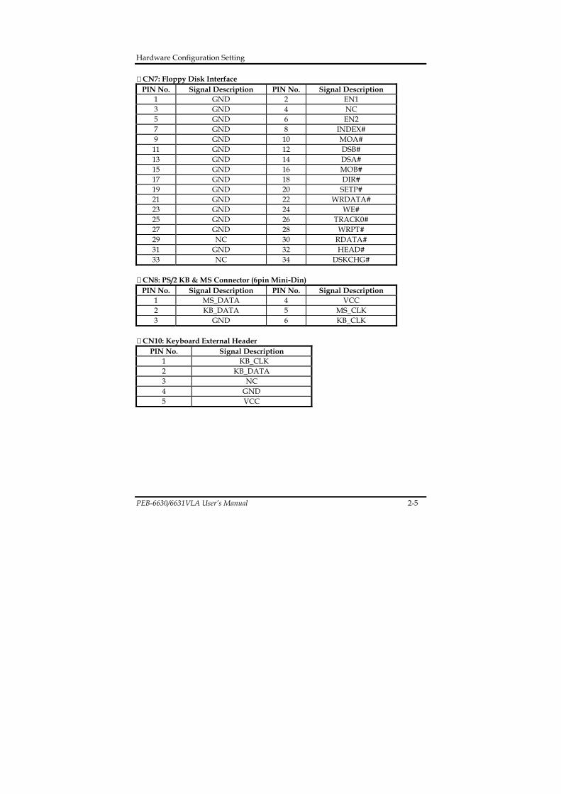
CN7: Floppy Disk Interface PIN No. Signal Description PIN No. Signal Description
1 GND 2 EN1 3 GND 4 NC 5 GND 6 EN2 7 GND 8 INDEX# 9 GND 10 MOA# 11 GND 12 DSB# 13 GND 14 DSA# 15 GND 16 MOB# 17 GND 18 DIR# 19 GND 20 SETP# 21 GND 22 WRDATA# 23 GND 24 WE# 25 GND 26 TRACK0# 27 GND 28 WRPT# 29 NC 30 RDATA# 31 GND 32 HEAD# 33 NC 34 DSKCHG#
CN8: PS/2 KB & MS Connector (6pin Mini-Din) PIN No. Signal Description PIN No. Signal Description
1 MS_DATA 4 VCC 2 KB_DATA 5 MS_CLK 3 GND 6 KB_CLK
CN10: Keyboard External Header
PIN No. Signal Description 1 KB_CLK 2 KB_DATA 3 NC 4 GND 5 VCC

Hardware Configuration Setting
PEB-6630/6631VLA User’s Manual 2-6
CN12: VGA DSUB-15 Connector PIN No. Signal Description PIN No. Signal Description
1 RED 9 VCC 2 GREEN 10 GND 3 BLUE 11 NC 4 NC 12 DATA 5 GND 13 HSYNC 6 GND 14 VSYNC 7 GND 15 CLK 8 GND
CN13: Flat Panel Display Connector PIN No. Signal Description PIN No. Signal Description
1 TX1+ 2 TX2+ 3 TX1- 4 TX2- 5 GND 6 GND 7 GND 8 GND 9 TXC+ 10 TX0+ 11 TXC- 12 TX0- 13 GND 14 GND 15 VCC 16 NC 17 VCC 18 DATA 19 VCC 20 CLK
CN14: ATX Power Control
PIN No. Signal Description 1 POWER_OK 2 ATX5VSB 3 PWR_ON# 4 GND

Hardware Configuration Setting
PEB-6630/6631VLA User’s Manual 2-7
CN15: IDE Interface PIN No. Signal Description PIN No. Signal Description
1 Reset 2 D7 3 D7 4 D8 5 D6 6 D9 7 D5 8 D10 9 D4 10 D11 11 D3 12 D12 13 D2 14 D13 15 D1 16 D14 17 D0 18 D15 19 Ground 20 NC 21 DREQ 22 Ground 23 IOW 24 Ground 25 IOR 26 Ground 27 IORDY 28 Pull Down 29 DACK 30 Ground 31 IRQ14 32 CS16 33 DA1 34 NC 35 DA0 36 DA2 37 CS1 38 CS3 39 ACTIVE 40 Ground
CN17: Ethernet RJ-45 Interface Connector
PIN No. Signal Description 1 TX+ 2 TX- 3 TDC 4 GND 5 GND 6 RDC 7 RX+ 8 RX- 9 GREEN +
10 GREEN - 11 YELLOW + 12 YELLOW -

Hardware Configuration Setting
PEB-6630/6631VLA User’s Manual 2-8
CN18: CD-ROM LINE-IN and MIC-IN Interface Connector PIN No. Signal Description PIN No. Signal Description
1 CD_R 5 MIC_IN 2 GND 6 GND 3 GND 7 GND 4 CD_L 8 VREFOUT
CN19: Dual Universal Serial BUS Stack Up Connector PIN No. Signal Description PIN No. Signal Description
1 OC0 5 OC1 2 P0- 6 P1- 3 P0+ 7 P1+ 4 Ground 8 Ground
CN20: LINE-IN and LINE-OUT Interface Connector PIN No. Signal Description PIN No. Signal Description
1 LINE_IN_R 4 LINE_OUT_R 2 GND 5 GND 3 GND 6 GND 4 LINE_IN_L 8 LINE_OUT_L
CN21: Standard Power Connector (BIG 4 PIN)
PIN No. Signal Description 1 +12V 2 Ground 3 Ground 4 +5V

Hardware Configuration Setting
PEB-6630/6631VLA User’s Manual 2-9
CN22: Compact Flash Socket PIN No. Signal Description PIN No. Signal Description
1 Ground 26 CD1 2 D3 27 D11 3 D4 28 D12 4 D5 29 D13 5 D6 30 D14 6 D7 31 D15 7 CS1 32 CS3 8 A10 33 VS1 9 Output Enable 34 IOR 10 A9 35 IOW 11 A8 36 Write Enable 12 A7 37 IRQ 13 +5V 38 +5V 14 A6 39 CSEL 15 A5 40 VS2 16 A4 41 RESET 17 A3 42 IORDY 18 A2 43 DREQ 19 A1 44 DACK 20 A0 45 VD2 21 D0 46 VD1 22 D1 47 D8 23 D2 48 D9 24 CS16 49 D10 25 CD2 50 Ground

Hardware Configuration Setting
PEB-6630/6631VLA User’s Manual 2-10
PCI1: PCI Gold Finger PIN No. Signal Description PIN No. Signal Description
B1 -12V A1 TRST# B2 TCK A2 +12V B3 GND A3 TMS B4 TDO A4 TDI B5 +5V A5 +5V B6 +5V A6 INTA# B7 INTB# A7 INTC# B8 INTD# A8 +5V B9 REQ3# A9 PCI_CLK3
B10 REQ1# A10 +5V B11 GNT3# A11 PCI_CLK4 B12 GND A12 GND B13 GND A13 GND B14 PCI_CLK1 A14 GNT1# B15 GND A15 RESET# B16 PCK_CLK2 A16 +5V B17 GND A17 GNT0# B18 REQ0# A18 GND B19 +5V A19 REQ2# B20 AD31 A20 AD30 B21 AD29 A21 GND B22 GND A22 AD28 B23 AD27 A23 AD26 B24 AD25 A24 GND B25 +3.3V A25 AD24 B26 C/BE#3 A26 GNT2# B27 AD23 A27 +3.3V B28 GND A28 AD22 B29 AD21 A29 AD20 B30 AD19 A30 GND B31 +3.3V A31 AD18 B32 AD17 A32 AD16 B33 C/BE#2 A33 +3.3V B34 GND A34 FRAME# B35 IRDY# A35 GND B36 +3.3V A36 TRDY# B37 DEVSEL# A37 GND B38 GND A38 STOP#

Hardware Configuration Setting
PEB-6630/6631VLA User’s Manual 2-11
B39 LOCK# A39 +3.3V B40 PERR# A40 SDONE B41 +3.3V A41 SBO# B42 SERR# A42 GND B43 +3.3V A43 PAR B44 C/BE#1 A44 AD15 B45 AD14 A45 +3.3V B46 GND A46 AD13 B47 AD12 A47 AD11 B48 AD10 A48 GND B49 GND A49 AD9 B50 KEY A50 KEY B51 KEY A51 KEY B52 AD8 A52 C/BE#0 B53 AD7 A53 +3.3V B54 +3.3V A54 AD6 B55 AD5 A55 AD4 B56 AD3 A56 GND B57 GND A57 AD2 B58 AD1 A58 AD0 B59 +5V A59 +5V B60 ACK64# A60 REQ64# B61 +5V A61 +5V B62 +5V A62 +5V
**These power signals ( +12V & +3.3V ) are not into this PCI interface

System Installation
PEB-6630/6631VLA User’s Manual 3-1
CHAPTER 3 System Installation This chapter provides you with instructions to set up your system. The additional information is enclosed to help you set up onboard PCI device and handle WDT operation in software programming. 3.1 Low Voltage Intel Celeron/Pentium-III Processor Configuring System Bus PEB-6630/6631VLA will automatically detect system bus based on the CPU used. However, users may configure CPU core/bus ratio in BIOS setup menu for engineering sample processor. 3.2 Main Memory PEB-6630/6631VLA provides one DIMM socket (168-pin Dual In-line Memory Module) to support 3.3V SDRAM (Synchronized DRAM) as on-board main memory. The maximum memory size is 512MB. PEB-6630/6631VLA will automatically detect memory clock, based on the processor and SDRAM used. Please refer to the following table as your reference. PEB-6630/6631VLA Memory Clock Reference Table
Processor FSB PC-100SDRAM PC-133SDRAM 100MHz 100MHz 100MHz For system compatibility and stability, don’t use memory module without brand. You can also use single-sided or double-sided DIMM with ECC feature(2). Watch out the contact and lock integrity of memory module with socket, it will impact on the system reliability. Follow normal procedure to install your DRAM module into memory socket. Before locking, make sure that the module has been fully inserted into the card slot. NOTE: (1) To maintain system stability, don’t change any of DRAM parameters in BIOS
setup to upgrade your system performance without acquiring technical information.

System Installation
PEB-6630/6631VLA User’s Manual 3-2
(2) Due to Intel 82815-chipset limitation, SDRAM with ECC function is not
supported. In the event of ECC SDRAM being adopted, ECC function is NOT supported while it is still OK to use this type of SDRAM.
(3) Due to Intel 82815 chipset limitation, Buffered (Registered) SDRAM is not supported. Buffered SDRAM will simply freeze up or annoy your system.
3.3 Installing the Single Board Computer To install your PEB-6630/6631VLA into a standard chassis or proprietary environment, you need to perform the following: Step 1: Check all jumpers setting on proper position Step 2: Install and configure CPU and memory module on right position Step 3: Place PEB-6630/6631VLA into the dedicated position in your system Step 4: Attach cables to existing peripheral devices and secure it WARNING Please ensure that your SBC is properly inserted and fixed by mechanism. Otherwise, the system might be unstable or do not work due to bad contact of golden finger and PCI-bus slot. It is recommended to apply 4-pin 5-1/4” IDE device power connectors from your power supply onto CN21 to ensure a sufficient current supply. NOTE: Please refer to section 3-3-1 to 3-3-3 to install INF/VGA/LAN drivers. 3.3.1 INF Chipset Component Driver Intel 82815 GMCH chipset is a new chipset that a few old operating systems might not be able to recognize. To overcome this compatibility issue, for Windows Operating Systems such as Windows-95/98/98SE/2000, please install INF Chipset Component driver before any of other Drivers are installed. You can find very easily the INF chipset component driver in /INF directory of PEB-6630/6631VLA CD-title. Please execute “Setup.exe” to start installation.

System Installation
PEB-6630/6631VLA User’s Manual 3-3
3.3.2 Intel 82815 GMCH Graphics Controller Intel 82815 GMCH chipset is the result of new design approach to optimize the shared memory architecture while maintaining the cost benefits of integration through Direct AGP and Dynamic Video Memory Technology. With no additional video adaptor, this onboard video will be the system display output. However, system will automatically switch to off-board video adaptor if there is any. In this case, onboard 82815 GMCH graphic features will be disabled. There is no way to disable this onboard video function, unless one off-board PCI video card is applied onto the backplane. In this case, the off-board video card shall be picked up first based on the default BIOS setup (Initial Display First) in “Integrated Peripheral” Setup Menu. Drivers Support Please find Intel 82815 GMCH driver in /Graphics directory of PEB-6630/6631VLA CD-title. Drivers support Windows-3.1, Windows-95/98/98SE/ME, Windows-NT 3.51/4.0, Windows-2000, OS2, and Linux. (1) Windows-95: Please bring up the Display Control Panel and update graphics
driver with /Graphics/win9x/Graphics/Win9x/I81xw9x.inf.
(2) Windows-98/98SE/ME: Please execute /Graphics/win9x/Graphics/Setup.exe to start graphics drivers installation, or bring up the Display Control Panel and update graphics driver with /Graphics/win9x/Graphics/Win9x/I81xw9x.inf.
(3) Windows-NT 4.0: Please install Windows-NT 4.0 Service Pack 4 or above first, then
execute /Graphics/Winnt4/Graphics/Setup.exe, or simply bring up the Display Control Panel and update graphics driver with /Graphics/winnt4/Graphics/WinNT4/I81xNT4.inf.
(4) Windows-2000: Please bring up the Device Manager and update graphics drivers
with /Graphics/win2k/Graphics/Win2000/I81xNT5.inf. (5) Redhat Linux V6.2: Please refer to the “release_linux.pdf” readme file in
/Graphics/Linux directory for graphics drivers installation guide.

System Installation
PEB-6630/6631VLA User’s Manual 3-4
3.3.3 Intel 82801BA MAC Fast Ethernet Controller This Fast Ethernet function is supported by Intel 82801BA (ICH2) embedded PHY and interfaced via Intel 82562ET Platform LAN Connect (PLC). Drivers Support Please find LAN driver in /Ethernet directory of PEB-6630/6631VLA CD-title. The drivers support Windows-NT 3.51/4.0, Windows-95/98/98SE/ME, Windows-2000, and SCO OpenServer 5.0.2, SCO Unixware 7.0, OS2 and Linux. In Windows environment, Intel 82801BA MAC Fast Ethernet should appear as Intel (R) PRO/100 VE Network Connection. On-board LED Indicator (for LAN status) PEB-6630/6631VLA provides two LED indicators with RJ-45 connector to report Intel 82801BA MAC Fast Ethernet interfaces status. Please refer to the table below as a quick reference guide.
Operation of Ethernet Port Intel 82801BA
MAC Name of LED
ON Off
Amber LAN speed LED 100 Mbps 10 Mbps Green LAN active LED Active No active Green LAN Link Integrity LED Good link in 10 or 100 Mbps No link
There is no way to disable this onboard Ethernet function. 3.3.4 Intel 82801BA AC’97 Codec Controller This on-board Audio function is supported by Intel 82801BA (ICH2) embedded AC’97 Codec Controller. Drivers Support Please find Sound driver in /Sound directory of PEB-6630/6631VLA CD-title. The drivers support Windows-NT 3.51/4.0, Windows-95/98/98SE, and Windows-2000. To disable this onboard Audio function, please configure the “Integrated Peripheral” Setup Menu in BIOS. Change the “AC’97 Audio” setting to “Disabled” will help you to turn off this PCI Audio device.
System Installation
PEB-6630/6631VLA User’s Manual 3-5
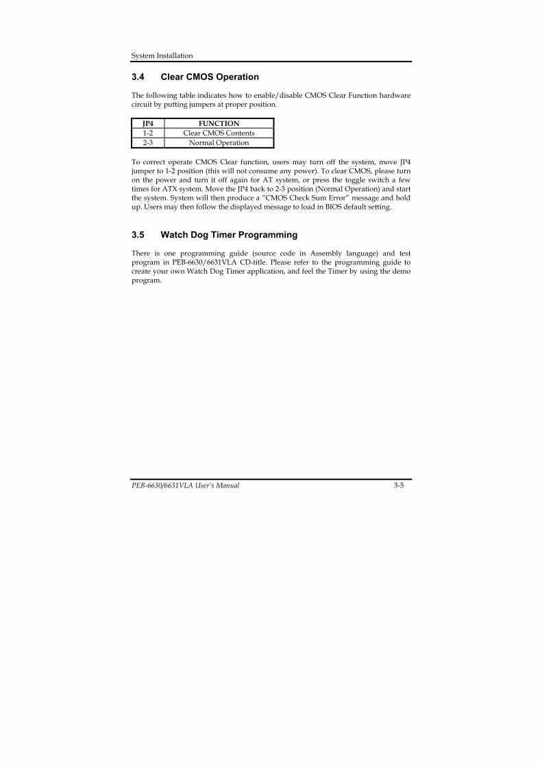
3.4 Clear CMOS Operation The following table indicates how to enable/disable CMOS Clear Function hardware circuit by putting jumpers at proper position.
JP4 FUNCTION 1-2 Clear CMOS Contents 2-3 Normal Operation
To correct operate CMOS Clear function, users may turn off the system, move JP4 jumper to 1-2 position (this will not consume any power). To clear CMOS, please turn on the power and turn it off again for AT system, or press the toggle switch a few times for ATX system. Move the JP4 back to 2-3 position (Normal Operation) and start the system. System will then produce a “CMOS Check Sum Error” message and hold up. Users may then follow the displayed message to load in BIOS default setting. 3.5 Watch Dog Timer Programming There is one programming guide (source code in Assembly language) and test program in PEB-6630/6631VLA CD-title. Please refer to the programming guide to create your own Watch Dog Timer application, and feel the Timer by using the demo program.
BIOS Setup Information
PEB-6630/6631VLA User’s Manual 4-1
CHAPTER 4 BIOS Setup Information PEB-6630/6631VLA is equipped with the AWARD BIOS stored in Flash ROM. This BIOS has a built-in Setup program that allows users to modify the basic system configuration easily. This type of information is stored in CMOS RAM so that it is retained during power-off periods. When system is turned on, PEB-6630/6631VLA communicates with peripheral devices and check its hardware resources against the configuration information stored in the CMOS memory. If any error is detected, or the CMOS parameters need to be initially defined, the diagnostic program will prompt the user to enter the SETUP program. Some errors are significant enough to abort the start-up. 4.1 Entering Setup Turn on or reboot the computer. When the message “Hit <DEL> if you want to run SETUP” appears, press <Del> key immediately to enter BIOS setup program. If the message disappears before you respond, but you still wish to enter Setup, please restart the system to try “COLD START” again by turning it OFF and then ON, or touch the "RESET" button. You may also restart from “WARM START” by pressing <Ctrl>, <Alt>, and <Delete> keys simultaneously. If you do not press the keys at the right time and the system will not boot, an error message will be displayed and you will again be asked to, Press <F1> to Run SETUP or Resume In HIFLEX BIOS setup, you can use the keyboard to choose among options or modify the system parameters to match the options with your system. The table below will show you all of keystroke functions in BIOS setup.

BIOS Setup Information
PEB-6630/6631VLA User’s Manual 4-2
Keys to navigate within setup menu
Key Functions Up Arrow Move to the previous item
Down Arrow Move to the next item Left Arrow Move to the item on the left (menu bar)
Right Arrow Move to the item on the right (menu bar) Move Enter Move to the item you desired PgUp key Increase the numeric value or make changes PgDn key Decrease the numeric value or make changes
+ key Increase the numeric value or make changes - key Decrease the numeric value or make changes
Esc key Main Menu -- Quit and not save changes into CMOS Status Page Setup Menu and Option Page Setup Menu -- Exit current page and return to Main Menu
F1 key General help on Setup navigation keys F5 key Load previous values from CMOS F6 key Load the fail-safe defaults from BIOS default table F7 key Load the optimized defaults
F10 key Save all the CMOS changes and exit

BIOS Setup Information
PEB-6630/6631VLA User’s Manual 4-3
4.2 Main Menu Once you enter PEB-6630/6631VLA AWARD BIOS CMOS Setup Utility, you should start with the Main Menu. The Main Menu allows you to select from eleven setup functions and two exit choices. Use arrow keys to switch among items and press <Enter> key to accept or bring up the sub-menu.
NOTE : It is strongly recommended to reload the Optimized Default Setting if
CMOS is lost or BIOS is updated.

BIOS Setup Information
PEB-6630/6631VLA User’s Manual 4-4
4.3 Standard CMOS Setup Menu This setup page includes all the items in a standard compatible BIOS. Use the arrow keys to highlight the item and then use the <PgUp>/<PgDn> or <+>/<-> keys to select the value or number you want in each item and press <Enter> key to certify it. Follow command keys in CMOS Setup table to change Date, Time, Drive type, and Boot Sector Virus Protection Status.

BIOS Setup Information
PEB-6630/6631VLA User’s Manual 4-5
Menu seletions
Item Options Description Date Mm:dd:yy Set the system date. Note that
the ‘Day’ automatically changes when you set the date
Time Hh:mm:ss Set the system time IDE Primary Master Options are in its sub menu
(described in 4.4 Table) Press <Enter> to enter the sub menu of detailed options
IDE Primary Slave Options are in its sub menu (described in 4.4 Table)
Press <Enter> to enter the sub menu of detailed options
IDE Secondary Master Options are in its sub menu (described in 4.4 Table)
Press <Enter> to enter the sub menu of detailed options
IDE Secondary Slave Options are in its sub menu (described in 4.4 Table)
Press <Enter> to enter the sub menu of detailed options
Drive A Drive B
None 360K, 5.25 in 1.2M, 5.25 in 720K, 3.5 in 1.44M, 3.5 in 2.88M, 3.5 in
Select the type of floppy disk drive installed in your system
Video EGA/VGA CGA 40 CGA 80 MONO
Select the default video device
Halt On All Errors No Errors
All, but Keyboard All, but Diskette
All, but Disk/Key
Select the situation in which you want the BIOS to stop the POST process and notify you
Base Memory N/A Displays the amount of conventional memory detected during boot up
Extended Memory N/A Displays the amount of extended memory detected during boot up
Total Memory N/A Displays the total memory available in the system

BIOS Setup Information
PEB-6630/6631VLA User’s Manual 4-6
4.4 IDE Adaptors Setup Menu The IDE adapters control the IDE devices, such as hard disk drive or cdrom drive. It uses a separate sub menu to configure each hard disk drive.
Remark: A 20 GB Hard Drive is used above for the demostration.

BIOS Setup Information
PEB-6630/6631VLA User’s Manual 4-7
Menu seletions
Item Options Description IDE HDD Auto-
detection Press Enter Press Enter to auto-detect the HDD on this
channel. If detection is successful, it fills the remaining fields on this menu.
IDE Primary Master None Auto
Manual
Selecting ‘manual’ lets you set the remaining fields on this screen. Selects the type of fixed disk. "User Type" will let you select the number of cylinders, heads, etc. NOTE: PRECOMP=65535 means NONE !
Capacity Auto Display your disk drive size
Disk drive capacity (Approximated). Note that this size is usually slightly greater than the size of a formatted disk given by a disk checking program.
Access Mode Normal LBA
Large Auto
Choose the access mode for this hard disk
The following options are selectable only if the ‘IDE Primary Master’ item is set to ‘Manual’
Cylinder Min = 0 Max = 65535
Set the number of cylinders for this hard disk.
Head Min = 0 Max = 255
Set the number of read/write heads
Precomp Min = 0 Max = 65535
**** Warning: Setting a value of 65535 means no hard disk
Landing zone Min = 0 Max = 65535
****
Sector Min = 0 Max = 255
Number of sectors per track

BIOS Setup Information
PEB-6630/6631VLA User’s Manual 4-8
4.5 Advanced BIOS Features This section allows you to configure your system for basic operation. You have the opportunity to select the system’s default speed, boot-up sequence, keyboard operation, shadowing and security.
Virus Warning
Enabled Activates automatically when the system boots up causing a warning message to appear when anything attempts to access the boot sector or hard disk partition table.
Disabled No warning message will appear when anything attempts to access the boot sector or hard disk partition table.
Quick Power On Self Test This category speeds up Power On Self Test (POST) after you power up the computer. If it is set to Enable, BIOS will shorten or skip some check items during POST.
Enabled Enable quick POST Disabled Normal POST
BIOS Setup Information
PEB-6630/6631VLA User’s Manual 4-9
First/Second/Third/Fourth Boot Device The BIOS attempts to load the operating system from the devices in the sequence selected in these items. The choices: Floppy, LS120, ZIP100, HDD, SCSI, CDROM, LAN, and Disabled. Boot Up NumLock Status Select power on state for NumLock. The choices: Enabled/Disabled. Typematic Rate Setting Key strokes repeat at a rate determined by the keyboard controller. When enabled, the typematic rate and typematic delay can be selected. The choices: Enabled/Disabled. Typematic Rate (Chars/Sec) Sets the number of times a second to repeat a key stroke when you hold the key down. The choices: 6, 8, 10, 12, 15, 20, 24, 30. Typematic Delay (Msec) Sets the delay time after the key is held down before it begins to repeat the keystroke. The choices: 250, 500, 750, 1000. Security Option Select whether the password is required every time the system boots or only when you enter setup.
System The system will not boot and access to Setup will be denied if the correct password is not entered at the prompt.
Setup The system will boot, but access to Setup will be denied if the correct password is not entered at the prompt.
BIOS Setup Information
PEB-6630/6631VLA User’s Manual 4-10
NOTE : To disable security, select PASSWORD SETTING at Main Menu and then you
will be asked to enter password. Do not type anything and just press <Enter>, it will disable security. Once the security is disabled, the system will boot and you can enter Setup freely.
OS Select For DRAM > 64MB Select the operating system that is running with greater than 64MB of RAM on the system. The choices: Non-OS2, OS2. HDD S.M.A.R.T. Capability This option allows users to enable/disable the PC to predict the future failure of hard drive. The choices: Enabled, Disabled.

BIOS Setup Information
PEB-6630/6631VLA User’s Manual 4-11
4.6 Advanced Chipset Features This section allows you to configure the system based on the specific features of the Intel 82815 GMCH chipset. This chipset manages bus speeds and access to system memory resources, such as DRAM (SDRAM) and the external cache. It also coordinates communications between the conventional ISA bus and the PCI bus. It must be stated that these items should never need to be altered. The default settings have been chosen because they provide the best operating conditions for your system. The only time you might consider making any changes would be if you discovered that data was being lost while using your system.
This chipset settings deal with CPU access to dynamic random access memory (DRAM). The default timings have been carefully chosen and should only be altered if data is being lost. Such a scenario might well occur if your system had mixed speed DRAM chips installed so that greater delays may be required to preserve the integrity of the data held in the slower memory chips. SDRAM CAS Latency Time This option controls the number of SCLKs between the time a read command is sampled by the SDRAMs and the time the GMCH samples correspondent data from the SDRAMs. The choices: 2, 3 SCLKs.
BIOS Setup Information
PEB-6630/6631VLA User’s Manual 4-12
SDRAM Cycle Time Tras/Trc This option controls the number of SDRAM clocks used per access cycle. The choices: 5/7, 7/9. SDRAM RAS-to-CAS Delay This option controls the number of SCLKs (SDRAM Clock) from a row activate command to a read or write command. If your system installs good quality of SDRAM, you can set this option to “3 SCLKs” to obtain better memory performance. Normally, the option will be set to 3 SCLKs. The choices: 2, 3 SCLKs. SDRAM RAS Precharge Time This option controls the number of SCLKs for RAS# precharge. If your system installs good quality of SDRAM, you can set this option to “3 SCLKs” to obtain better memory performance. The choices: 2, 3 SCLKs. System BIOS Cacheable Selecting Enabled allows caching of the system BIOS ROM at F0000h-FFFFFh, resulting in better system performance. However, if any program writes to this memory area, a system error may result. The choices: Enabled/Disabled. Video BIOS Cacheable Select “Enabled” to enable caching VGA BIOS into L2 cache to get higher display performance. “Disabled” will ignore this BIOS caching function. The choices : Enabled/Disabled Memory Hole At 15-16M In order to improve performance, certain space in memory is reserved for ISA cards. This memory must be mapped into the memory space below 16MB. The choices: Enabled/Disabled.

BIOS Setup Information
PEB-6630/6631VLA User’s Manual 4-13
System Memory Frequency This option allows users to configure the system memory frequency. The default setting is Auto. The choices: 100MHz, 133MHz and Auto. On-Chip Video Window Size This option allows you to select the size of mapped memory for AGP graphic data. The choices: 64MB/Disabled. CAS# Latency This option selects in units of local memory clock periods. The choices: 2, 3 SCLKs. Paging Mode Control This option controls GMCH memory controller tends to leave pages open or pages close. The choices: Open / Close. RAS-to-CAS Override This option selects in units of display cache clock periods indicates the RAS#-to-CAS# delay. The choices: by CAS# LT / Override(2). RAS# Timing This option controls RAS# active to precharge, and refresh to RAS# active delay. The choices: Fast / Slow.

BIOS Setup Information
PEB-6630/6631VLA User’s Manual 4-14
RAS# Precharge Timing This option controls RAS# precharge in local memory clocks. The choices: Fast / Slow. 4.7 Integrated Peripherals
OnChip Primary/Secondary PCI IDE The chipset contains a PCI IDE interface with support for two IDE channels. Select Enabled to activate the primary IDE interface. Select Disabled to deactivate this interface The choices: Enabled/Disabled.

BIOS Setup Information
PEB-6630/6631VLA User’s Manual 4-15
IDE Primary/Secondary Master/Slave PIO The two IDE PIO (Programmed Input/Output) fields let you set a PIO mode (0-4) for each of the two IDE devices that the onboard IDE interface supports. Modes 0 through 4 provide successively increased performance. In Auto mode, the system automatically determines the best mode for each device. The choices: Auto, Mode 0, Mode 1, Mode 2, Mode 3, Mode 4. IDE Primary/Secondary Master/Slave UDMA Ultra DMA/33/66/100 implementation is possible only if your IDE hard drive supports it and the operating environment includes a DMA driver (Windows 95 OSR2 or a third-party IDE bus master driver). If your hard drive and your system software both support Ultra DMA/33/66/100, select Auto to enable BIOS support. The choices: Auto, Disabled. USB Controller This item allows you to enable/disable USB (Universal Serial Bus) function. The choices: Enabled/Disabled USB Keyboard Support This item allows you to enable USB keyboard function under POST, BIOS setup menu, DOS, or Windows-NT with no USB driver loaded. The choices: Enabled/Disabled Init Display First This item allows you to select the first display port to be initialized. The choices: PCI Slot (off-board video adaptor), Onboard/AGP AC97 Audio This item allows you to enable/disable the on-board audio. Default setting is Auto. The choices: Auto/Disabled

BIOS Setup Information
PEB-6630/6631VLA User’s Manual 4-16
IDE HDD Block Mode This item allows you to enable/disable IDE HDD Block Mode. The function is to collect the data that is nearby the one being read and leave them in the system buffer. Buffered data can be used with faster transmission rate so as to enhance system performance. The choices: Enabled/Disabled Power On Function This item allows you to select different power on scheme using ATX power supply.
Button Only Power on by power Button Keyboard 98 Power on by keyboard 98 Password Power on using customized password string
Keyboard Power On Password In the event of “Power On Function” being configured as “Password”, this item will be enabled for tuning. Press “Enter” key to enter a customized password, and confirm again when being asked. In the case that the confirmed password does not match the configured one, the message of “Password Disabled – Press any key to continue…” will be prompted. 4.8 Onboard FDC Controller This item allows you to enable/disable onboard Floppy disk controller. The choices: Enabled/Disabled 4.9 Onboard Serial Port 1/Port 2 Select an address and corresponding interrupt for the first and second serial ports. The choices: 3F8/IRQ4, 2E8/IRQ3, 3E8/IRQ4, 2F8/IRQ3, Disabled, Auto.

BIOS Setup Information
PEB-6630/6631VLA User’s Manual 4-17
4.10 UART Mode Select This item allows users to select Infrared transmission mode.
Normal Disable Infrared function IrDA Select IrDA mode transmission ASKIR Select ASKIR mode transmission
As Infrared transmission function shares onboard serial port 2, COM2 needs to be enabled. RxD, TxD Active This item is to configure Infrared transmission rate. Four options are available :
Hi, Hi High rate for receiving / High rate for transmitting Hi, Lo High rate for receiving / Low rate for transmitting Lo, Hi Low rate for receiving / High rate for transmitting Lo, Lo Low rate for receiving / Low rate for transmitting
Onboard Parallel Port This item allows you to configure I/O address of the onboard parallel port. The choices : Disabled, 378/IRQ7, 278/IRQ5, 3BC/IRQ7 Parallel Port Mode There are four different modes for the onboard parallel port :
SPP Switch to SPP mode EPP Switch to EPP mode ECP Switch to ECP mode ECP + EPP Switch to ECP + EPP mode
EPP Mode Select Select different version of EPP mode. The choices : EPP1.7/EPP1.9

BIOS Setup Information
PEB-6630/6631VLA User’s Manual 4-18
ECP Mode Use DMA Select a proper DMA channel for ECP mode. The choices : 3/1 PWRON After PWR-Fail This item allows user to configure the power status of using ATX power supply after a serious power loss occurs.
On System automatically restores power back Off System stays at power –off Former-Sts System restores back to previous status (On or Off)
Watch Dog Timer Select This item allows you to enable/disable WTD function. The choices : Enabled/Disabled

BIOS Setup Information
PEB-6630/6631VLA User’s Manual 4-19
4.11 Power Management Setup The Power Management Setup allows you to configure you system to most effectively save energy while operating in a manner consistent with your own style of computer use.
ACPI Function This item allows you to enable/disable the Advanced Configuration and Power Management (ACPI). The choices : Enabled/Disabled.

BIOS Setup Information
PEB-6630/6631VLA User’s Manual 4-20
Power Management This category allows you to select the type (or degree) of power saving and is directly related to “HDD Power Down”, “Suspend Mode”. There are three selections for Power Management, three of which have fixed mode settings.
Min. Power Saving Minimum power management. Suspend Mode = 1 hr., and HDD Power Down = 15 min.
Max. Power Saving Maximum power management. Suspend Mode = 1 min., and HDD Power Down = 1 min.
User Defined Allows you to set each mode individually. When not disabled, Suspend Mode ranges from 1 min. to 1 hr. and HDD Power Down ranges from 1 min. to 15 min.
Video Off Method This determines the manner in which the monitor is blanked.
V/H SYNC+Blank This selection will cause the system to turn off the vertical and horizontal synchronization ports and write blanks to the video buffer.
Blank Screen This option only writes blanks to the video buffer. DPMS Initial display power management signaling.
Video Off In Suspend This allows user to enable/disable video off in Suspend Mode. The choices : Yes/No Suspend Type Two options are available : Stop Grant and Power On Suspend. Suspend Mode When enabled and after the set time of system inactivity, all devices except the CPU will be shut off.

BIOS Setup Information
PEB-6630/6631VLA User’s Manual 4-21
HDD Power Down When enabled and after the set time of system inactivity, the hard disk drive will be powered down while all other devices remain active.
Soft-Off by PWR-BTTN This item allows users to set the time to remove the power after the power button is pressed. The choices : Instant-Off/Delay 4 Sec. Resume On Ring When select “Enabled”, a system that is at soft-off mode will be alert to Wake-On-Lan or Wake-On-Modem signal. The choices : Enabled/Disabled CPU Thermal-Throttling This item allows you to configure the CPU working duty cycle during suspend mode. The choices : 12.5%, 25.0%, 37.5%, 50.0%, 62.5%, 75.0%, 87.5% Resume by Alarm This item allows users to enable/disable the resume by alarm function. When “Enabled” is selected, system using ATX power supply could be powered on if a customized time and day is approached. Date(of Month) Alarm When “Resume by Alarm” is enabled, this item could allow users to configure the date parameter of the timing dateline on which to power on the systm. The choices : 0 ~ 31 Time(hh:mm:ss) Alarm When “Resume by Alarm” is enabled, this item could allow users to configure the time parameter of the timing dateline on which to power on the systm. The choices : hh (0~23), mm (0~59), ss (0 ~59)

BIOS Setup Information
PEB-6630/6631VLA User’s Manual 4-22
Primary/Secondary IDE 0/1 This item is to configure IDE devices being monitored by system so as to keep system out of suspend mode if the associated device is busy. The choices : Enabled/Disabled FDD, COM, LPT Port This item is to configure floppy device, COM ports, and parallel port being monitored by system so as to keep system out of suspend mode if the associated device is busy. The choices : Enabled/Disabled PCI PIRQ[A-D]# This item is to enable/disable the IRQ setting over the PCI slots. The choices : Enabled/Disabled

BIOS Setup Information
PEB-6630/6631VLA User’s Manual 4-23
4.12 PnP/PCI Configuration Setup This section describes configuring the PCI bus system. PCI, or Personal Computer Interconnect, is a system which allows I/O devices to operate at speeds nearing the speed the CPU itself uses when communicating with its own special components. This section covers some very technical items and it is strongly recommended that only experienced users should make any changes to the default settings.
Reset Configuration Data Normally, you leave this field Disabled. Select Enabled to reset Extended System Configuration Data (ESCD) when you exit Setup if you have installed a new add-on card and the system reconfiguration has caused such a serious conflict that the operating system can not boot. The choices: Enabled, Disabled .

BIOS Setup Information
PEB-6630/6631VLA User’s Manual 4-24
Resource controlled by The Award Plug and Play BIOS has the capacity to automatically configure all of the boot and Plug and Play compatible devices. However, this capability means absolutely nothing unless you are using a Plug and Play operating system such as Windows95. If you set this field to “manual” choose specific resources by going into each of the sub menu that follows this field (a sub menu is preceded by a “ ”). The choices: Auto (ESCD), Manual. IRQ Resources When resources are controlled manually, assign each system interrupt a type, depending on the type of device using the interrupt. It allows you to determine the IRQ assigned to the ISA bus and is not available to any PCI slot. Legacy ISA for devices compliant with the original PC AT bus specification, PCI/ISA PnP for devices compliant with the Plug and Play standard whether designed for PCI or ISA bus architecture. The choices: “Legacy ISA” and “PCI/ISA PnP” DMA Resources When resources are controlled manually, assign each system DMA channel a type, depending on the type of device using the DM channel. Legacy ISA for devices compliant with the original PC AT bus specification, PCI/ISA PnP for devices compliant with the Plug and Play standard whether designed for PCI or ISA bus architecture. The choices: “Legacy ISA” and “PCI/ISA PnP” PCI/VGA Palette Snoop Leave this field at Disabled. The choices : Enabled/Disabled.

BIOS Setup Information
PEB-6630/6631VLA User’s Manual 4-25
4.13 PC Health Status
4.14 Frequency/Voltage Control

BIOS Setup Information
PEB-6630/6631VLA User’s Manual 4-26
Auto Detect DIMM CLK This item allows you to enable/disable auto detect DIMM Clock The choices : Enabled, Disabled Spread Spectrum This item allows you to enable/disable the spread spectrum modulate The choices : Enabled, Disabled 4.15 Default Menu Selecting “Defaults” from the main menu shows you two options which are described below Load Fail-Safe Defaults When you press <Enter> on this item you get a confirmation dialog box with a message similar to: Load Fail-Safe Defaults (Y/N) ? N Pressing ‘Y’ loads the BIOS default values for the most stable, minimal-performance system operations. Load Optimized Defaults When you press <Enter> on this item you get a confirmation dialog box with a message similar to: Load Optimized Defaults (Y/N) ? N Pressing ‘Y’ loads the default values that are factory settings for optimal performance system operations.

BIOS Setup Information
PEB-6630/6631VLA User’s Manual 4-27
4.16 Supervisor/User Password Setting You can set either supervisor or user password, or both of then. The differences between are: supervisor password : can enter and change the options of the setup menus. user password : just can only enter but do not have the right to change the options of the setup menus. When you select this function, the following message will appear at the center of the screen to assist you in creating a password. ENTER PASSWORD Type the password, up to eight characters in length, and press <Enter>. The password typed now will clear any previously entered password from CMOS memory. You will be asked to confirm the password. Type the password again and press <Enter>. You may also press <Esc> to abort the selection and not enter a password. To disable a password, just press <Enter> when you are prompted to enter the password. A message will confirm the password will be disabled. Once the password is disabled, the system will boot and you can enter Setup freely. PASSWORD DISABLED When a password has been enabled, you will be prompted to enter it every time you try to enter Setup. This prevents an unauthorized person from changing any part of your system configuration. Additionally, when a password is enabled, you can also require the BIOS to request a password every time your system is rebooted. This would prevent unauthorized use of your computer. You determine when the password is required within the BIOS Features Setup Menu and its Security option (see Section 3). If the Security option is set to “System”, the password will be required both at boot and at entry to Setup. If set to “Setup”, prompting only occurs when trying to enter Setup.

BIOS Setup Information
PEB-6630/6631VLA User’s Manual 4-28
4.17 Exiting Selecting Save & Exit Setup Pressing <Enter> on this item asks for confirmation: Save to CMOS and EXIT (Y/N)? Y Pressing “Y” stores the selections made in the menus in CMOS – a special section of memory that stays on after you turn your system off. The next time you boot your computer, the BIOS configures your system according to the Setup selections stored in CMOS. After saving the values the system is restarted again. Exit Without Saving Pressing <Enter> on this item asks for confirmation: Quit without saving (Y/N)? Y This allows you to exit Setup without storing in CMOS any change. The previous selections remain in effect. This exits the Setup utility and restarts your computer. 4.18 POST Messages During the Power On Self-Test (POST), if the BIOS detects an error requiring you to do something to fix, it will either sound a beep code or display a message. If a message is displayed, it will be accompanied by: PRESS F1 TO CONTINUE, CTRL-ALT-ESC OR DEL TO ENTER SETUP POST Beep Currently there are two kinds of beep codes in BIOS. This code indicates that a video error has occurred and the BIOS cannot initialize the video screen to display any additional information. This beep code consists of a single long beep followed by two short beeps. The other code indicates that your DRAM error has occurred. This beep code consists of a single long beep repeatedly. Error Messages One or more of the following messages may be displayed if the BIOS detects an error during the POST. This list includes messages for both the ISA and the EISA BIOS.

BIOS Setup Information
PEB-6630/6631VLA User’s Manual 4-29
CMOS BATTERY HAS FAILED CMOS battery is no longer functional. It should be replaced. CMOS CHECKSUM ERROR Checksum of CMOS is incorrect. This can indicate that CMOS has become corrupt. This error may have been caused by a weak battery. Check the battery and replace if necessary. DISK BOOT FAILURE, INSERT SYSTEM DISK AND PRESS ENTER No boot device was found. This could mean that either a boot drive was not detected or the drive does not contain proper system boot files. Insert a system disk into Drive A: and press <Enter>. If you assumed the system would boot from the hard drive, make sure the controller is inserted correctly and all cables are properly attached. Also be sure the disk is formatted as a boot device. Then reboot the system. DISKETTE DRIVES OR TYPES MISMATCH ERROR - RUN SETUP Type of diskette drive installed in the system is different from the CMOS definition. Run Setup to reconfigure the drive type correctly. DISPLAY SWITCH IS SET INCORRECTLY Display switch on the motherboard can be set to either monochrome or color. This indicates the switch is set to a different setting than indicated in Setup. Determine which setting is correct, and then either turn off the system and change the jumper, or enter Setup and change the VIDEO selection. DISPLAY TYPE HAS CHANGED SINCE LAST BOOT Since last powering off the system, the display adapter has been changed. You must configure the system for the new display type. EISA Configuration Checksum Error PLEASE RUN EISA CONFIGURATION UTILITY The EISA non-volatile RAM checksum is incorrect or cannot correctly read the EISA slot. This can indicate either the EISA non-volatile memory has become corrupt or the slot has been configured incorrectly. Also be sure the card is installed firmly in the slot.

BIOS Setup Information
PEB-6630/6631VLA User’s Manual 4-30
EISA Configuration Is Not Complete PLEASE RUN EISA CONFIGURATION UTILITY The slot configuration information stored in the EISA non-volatile memory is incomplete. NOTE: When either of these errors appear, the system will boot in ISA mode, which
allows you to run the EISA Configuration Utility. ERROR ENCOUNTERED INITIALIZING HARD DRIVE Hard drive cannot be initialized. Be sure the adapter is installed correctly and all cables are correctly and firmly attached. Also be sure the correct hard drive type is selected in Setup. ERROR INITIALIZING HARD DISK CONTROLLER Cannot initialize controller. Make sure the cord is correctly and firmly installed in the bus. Be sure the correct hard drive type is selected in Setup. Also check to see if any jumper needs to be set correctly on the hard drive. FLOPPY DISK CNTRLR ERROR OR NO CNTRLR PRESENT Cannot find or initialize the floppy drive controller. make sure the controller is installed correctly and firmly. If there are no floppy drives installed, be sure the Diskette Drive selection in Setup is set to NONE. Invalid EISA Configuration PLEASE RUN EISA CONFIGURATION UTILITY The non-volatile memory containing EISA configuration information was programmed incorrectly or has become corrupt. Re-run EISA configuration utility to correctly program the memory. NOTE: When this error appears, the system will boot in ISA mode, which allows you
to run the EISA Configuration Utility. KEYBOARD ERROR OR NO KEYBOARD PRESENT Cannot initialize the keyboard. Make sure the keyboard is attached correctly and no keys are being pressed during the boot.

BIOS Setup Information
PEB-6630/6631VLA User’s Manual 4-31
If you are purposely configuring the system without a keyboard, set the error halt condition in Setup to HALT ON ALL, BUT KEYBOARD. This will cause the BIOS to ignore the missing keyboard and continue the boot. Memory Address Error at ... Indicates a memory address error at a specific location. You can use this location along with the memory map for your system to find and replace the bad memory chips. Memory parity Error at ... Indicates a memory parity error at a specific location. You can use this location along with the memory map for your system to find and replace the bad memory chips. MEMORY SIZE HAS CHANGED SINCE LAST BOOT Memory has been added or removed since the last boot. In EISA mode use Configuration Utility to reconfigure the memory configuration. In ISA mode enter Setup and enter the new memory size in the memory fields. Memory Verify Error at ... Indicates an error verifying a value already written to memory. Use the location along with your system's memory map to locate the bad chip. OFFENDING ADDRESS NOT FOUND This message is used in conjunction with the I/O CHANNEL CHECK and RAM PARITY ERROR messages when the segment that has caused the problem cannot be isolated. OFFENDING SEGMENT: This message is used in conjunction with the I/O CHANNEL CHECK and RAM PARITY ERROR messages when the segment that has caused the problem has been isolated. PRESS A KEY TO REBOOT This will be displayed at the bottom screen when an error occurs that requires you to reboot. Press any key and the system will reboot.

BIOS Setup Information
PEB-6630/6631VLA User’s Manual 4-32
PRESS F1 TO DISABLE NMI, F2 TO REBOOT When BIOS detects a Non-maskable Interrupt condition during boot, this will allow you to disable the NMI and continue to boot, or you can reboot the system with the NMI enabled. RAM PARITY ERROR - CHECKING FOR SEGMENT ... Indicates a parity error in Random Access Memory. Should Be Empty But EISA Board Found PLEASE RUN EISA CONFIGURATION UTILITY A valid board ID was found in a slot that was configured as having no board ID. NOTE: When this error appears, the system will boot in ISA mode, which allows you
to run the EISA Configuration Utility. Should Have EISA Board But Not Found PLEASE RUN EISA CONFIGURATION UTILITY The board installed is not responding to the ID request, or no board ID has been found in the indicated slot. NOTE: When this error appears, the system will boot in ISA mode, which allows you
to run the EISA Configuration Utility. Slot Not Empty Indicates that a slot designated as empty by the EISA Configuration Utility actually contains a board. NOTE: When this error appears, the system will boot in ISA mode, which allows you
to run the EISA Configuration Utility. SYSTEM HALTED, (CTRL-ALT-DEL) TO REBOOT ... Indicates the present boot attempt has been aborted and the system must be rebooted. Press and hold down the CTRL and ALT keys and press DEL.

BIOS Setup Information
PEB-6630/6631VLA User’s Manual 4-33
Wrong Board In Slot PLEASE RUN EISA CONFIGURATION UTILITY The board ID does not match the ID stored in the EISA non-volatile memory. NOTE: When this error appears, the system will boot in ISA mode, which allows you
to run the EISA Configuration Utility. FLOPPY DISK(S) fail (80) → Unable to reset floppy subsystem. FLOPPY DISK(S) fail (40) → Floppy Type mismatch. Hard Disk(s) fail (80) → HDD reset failed Hard Disk(s) fail (40) → HDD controller diagnostics failed. Hard Disk(s) fail (20) → HDD initialization error. Hard Disk(s) fail (10) → Unable to recalibrate fixed disk. Hard Disk(s) fail (08) → Sector Verify failed. Keyboard is locked out - Unlock the key. Keyboard error or no keyboard present.
Cannot initialize the keyboard. Make sure the keyboard is attached correctly and no keys are being pressed during the boot. BIOS ROM checksum error - System halted. The checksum of ROM address F0000H-FFFFFH is bad. Memory test fail. BIOS reports the memory test fail if the onboard memory is tested error.
BIOS Setup Information
PEB-6630/6631VLA User’s Manual 4-34
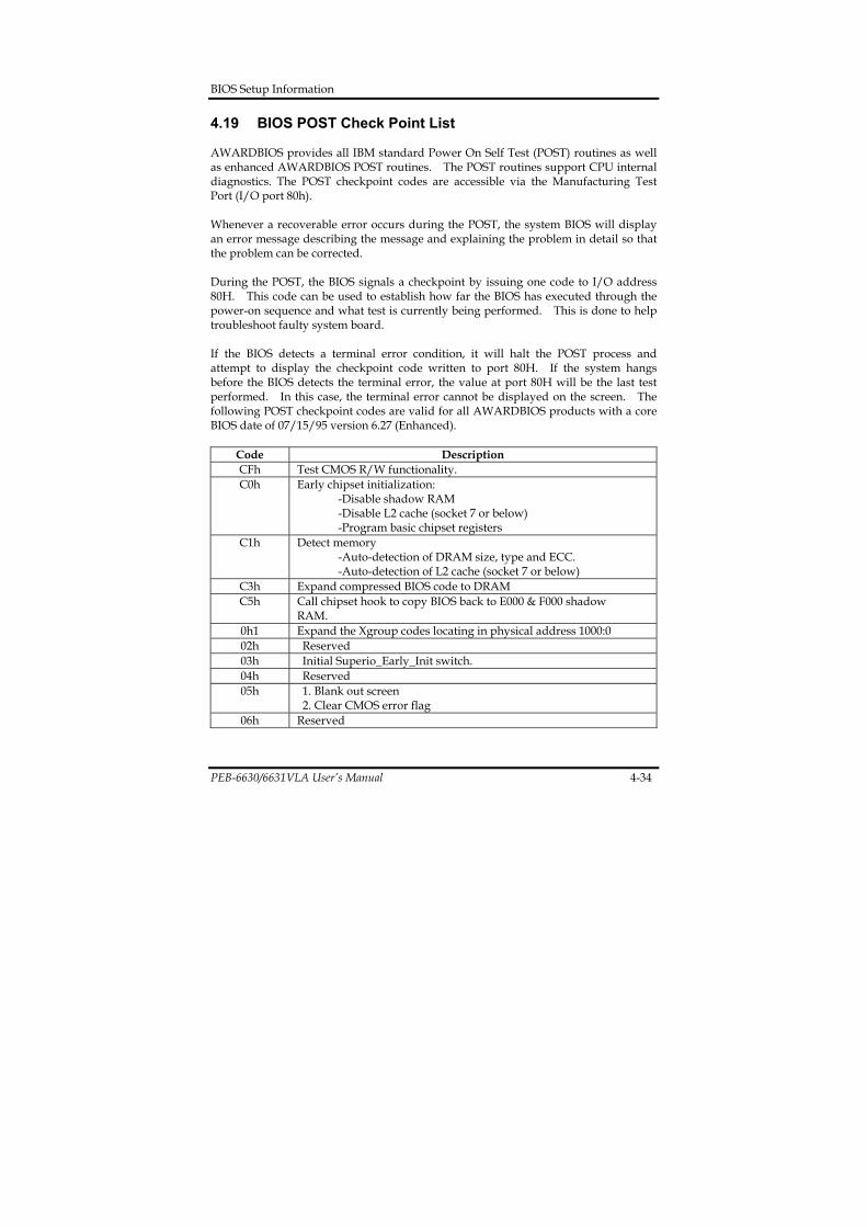
4.19 BIOS POST Check Point List AWARDBIOS provides all IBM standard Power On Self Test (POST) routines as well as enhanced AWARDBIOS POST routines. The POST routines support CPU internal diagnostics. The POST checkpoint codes are accessible via the Manufacturing Test Port (I/O port 80h). Whenever a recoverable error occurs during the POST, the system BIOS will display an error message describing the message and explaining the problem in detail so that the problem can be corrected. During the POST, the BIOS signals a checkpoint by issuing one code to I/O address 80H. This code can be used to establish how far the BIOS has executed through the power-on sequence and what test is currently being performed. This is done to help troubleshoot faulty system board. If the BIOS detects a terminal error condition, it will halt the POST process and attempt to display the checkpoint code written to port 80H. If the system hangs before the BIOS detects the terminal error, the value at port 80H will be the last test performed. In this case, the terminal error cannot be displayed on the screen. The following POST checkpoint codes are valid for all AWARDBIOS products with a core BIOS date of 07/15/95 version 6.27 (Enhanced).
Code Description CFh Test CMOS R/W functionality. C0h Early chipset initialization:
-Disable shadow RAM -Disable L2 cache (socket 7 or below) -Program basic chipset registers
C1h Detect memory -Auto-detection of DRAM size, type and ECC. -Auto-detection of L2 cache (socket 7 or below)
C3h Expand compressed BIOS code to DRAM C5h Call chipset hook to copy BIOS back to E000 & F000 shadow
RAM. 0h1 Expand the Xgroup codes locating in physical address 1000:0 02h Reserved 03h Initial Superio_Early_Init switch. 04h Reserved 05h 1. Blank out screen
2. Clear CMOS error flag 06h Reserved

BIOS Setup Information
PEB-6630/6631VLA User’s Manual 4-35
07h 1. Clear 8042 interface
2. Initialize 8042 self-test 08h 1. Test special keyboard controller for Winbond 977 series Super
I/O chips. 2. Enable keyboard interface.
09h Reserved 0Ah Disable PS/2 mouse interface (optional). Auto detect ports for
keyboard & mouse followed by a port & interface swap (optional). Reset keyboard for Winbond 977 series Super I/O chips.
0Bh Reserved 0Ch Reserved 0Dh Reserved 0Eh Test F000h segment shadow to see whether it is R/W-able or not. If
test fails, keep beeping the speaker. 0Fh Reserved 10h Auto detect flash type to load appropriate flash R/W codes into the
run time area in F000 for ESCD & DMI support. 11h Reserved 12h Use walking 1’s algorithm to check out interface in CMOS circuitry.
Also set real-time clock power status, and then check for override. 13h Reserved 14h Program chipset default values into chipset. Chipset default values are
MODBINable by OEM customers. 15h Reeserved 16h Initial Early_Init_Onboard_Generator switch. 17h Reserved 18h Detect CPU information including brand, SMI type (Cyrix or Intel)
and CPU level (586 or 686). 19h Reserved 1Ah Reserved 1Bh Initial interrupts vector table. If no special specified, all H/W
interrupts are directed to SPURIOUS_INT_HDLR & S/W interrupts to SPURIOUS_soft_HDLR.
1Ch Reserved 1Dh Initial EARLY_PM_INIT switch. 1Eh Reserved 1Fh Load keyboard matrix (notebook platform) 20h Reserved 21h HPM initialization (notebook platform) 22h Reserved

BIOS Setup Information
PEB-6630/6631VLA User’s Manual 4-36
23h 1. Check validity of RTC value:
e.g. a value of 5Ah is an invalid value for RTC minute. 2. Load CMOS settings into BIOS stack. If CMOS checksum fails, use default value instead. 3. Prepare BIOS resource map for PCI & PnP use. If ESCD is valid, take into consideration of the ESCD’s legacy information. 4. Onboard clock generator initialization. Disable respective clock resource to empty PCI & DIMM slots. 5. Early PCI initialization: -Enumerate PCI bus number
-Assign memory & I/O resource -Search for a valid VGA device & VGA BIOS, and put it
into C000:0. 24h Reserved 25h Reserved 26h Reserved 27h Initialize INT 09 buffer 28h Reserved 29h Program CPU internal MTRR (P6 & PII) for 0-640K memory address.
Initialize the APIC for Pentium class CPU. Program early chipset according to CMOS setup. Example: onboard IDE controller. Measure CPU speed. Invoke video BIOS.
2Ah Reserved 2Bh Reserved 2Ch Reserved 2Dh Initialize multi-language. Put information on screen display, including
Award title, CPU type, CPU speed …. 2Eh Reserved 2Fh Reserved 30h Reserved 31h Reserved 32h Reserved 33h Reset keyboard except Winbond 977 series Super I/O chips. 34h Reserved 35h Reserved 36h Reserved 37h Reserved 38h Reserved 39h Reserved 3Ah Reserved 3Bh Reserved
BIOS Setup Information
PEB-6630/6631VLA User’s Manual 4-37
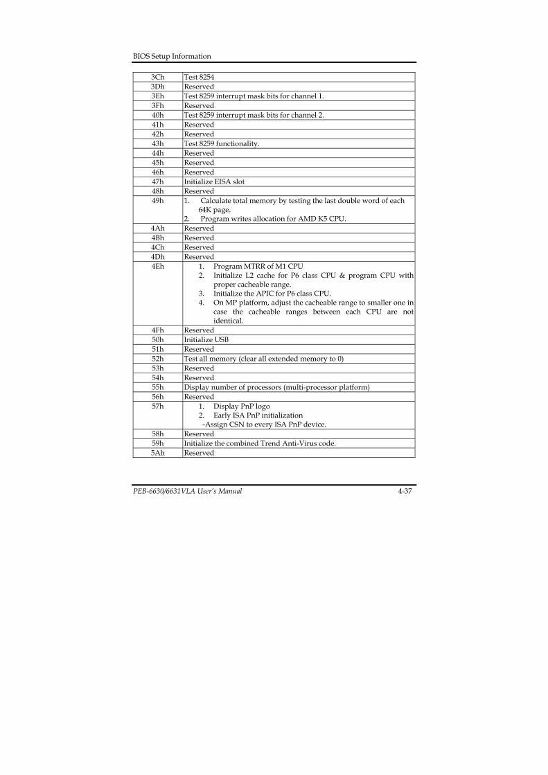
3Ch Test 8254 3Dh Reserved 3Eh Test 8259 interrupt mask bits for channel 1. 3Fh Reserved 40h Test 8259 interrupt mask bits for channel 2. 41h Reserved 42h Reserved 43h Test 8259 functionality. 44h Reserved 45h Reserved 46h Reserved 47h Initialize EISA slot 48h Reserved 49h 1. Calculate total memory by testing the last double word of each
64K page. 2. Program writes allocation for AMD K5 CPU.
4Ah Reserved 4Bh Reserved 4Ch Reserved 4Dh Reserved 4Eh 1. Program MTRR of M1 CPU
2. Initialize L2 cache for P6 class CPU & program CPU with proper cacheable range.
3. Initialize the APIC for P6 class CPU. 4. On MP platform, adjust the cacheable range to smaller one in
case the cacheable ranges between each CPU are not identical.
4Fh Reserved 50h Initialize USB 51h Reserved 52h Test all memory (clear all extended memory to 0) 53h Reserved 54h Reserved 55h Display number of processors (multi-processor platform) 56h Reserved 57h 1. Display PnP logo
2. Early ISA PnP initialization -Assign CSN to every ISA PnP device.
58h Reserved 59h Initialize the combined Trend Anti-Virus code. 5Ah Reserved

BIOS Setup Information
PEB-6630/6631VLA User’s Manual 4-38
5Bh (Optional Feature)
Show message for entering AWDFLASH.EXE from FDD (optional) 5Ch Reserved 5Dh 1. Initialize Init_Onboard_Super_IO switch.
2. Initialize Init_Onbaord_AUDIO switch. 5Eh Reserved 5Fh Reserved 60h Okay to enter Setup utility; i.e. not until this POST stage can users
enter the CMOS setup utility. 61h Reserved 62h Reserved 63h Reserved 64h Reserved 65h Initialize PS/2 Mouse 66h Reserved 67h Prepare memory size information for function call:
INT 15h ax=E820h 68h Reserved 69h Turn on L2 cache 6Ah Reserved 6Bh Program chipset registers according to items described in Setup &
Auto-configuration table. 6Ch Reserved 6Dh Assign resources to all ISA PnP devices.
Auto assign ports to onboard COM ports if the corresponding item in Setup is set to “AUTO”.
6Eh Reserved 6Fh 1. Initialize floppy controller
2. Set up floppy related fields in 40:hardware. 70h Reserved 71h Reserved 72h Reserved 73h (Optional Feature)
Enter AWDFLASH.EXE if : -AWDFLASH is found in floppy drive. -ALT+F2 is pressed
74h Reserved 75h Detect & install all IDE devices: HDD, LS120, ZIP, CDROM….. 76h Reserved 77h Detect serial ports & parallel ports. 78h Reserved 79h Reserved

BIOS Setup Information
PEB-6630/6631VLA User’s Manual 4-39
7Ah Detect & install co-processor 7Bh Reserved 7Ch Reserved 7Dh Reserved 7Eh Reserved 7Fh 1. Switch back to text mode if full screen logo is supported.
-If errors occur, report errors & wait for keys -If no errors occur or F1 key is pressed to continue: Clear EPA or customization logo.
80h Reserved 81h Reserved 82h 1. Call chipset power management hook.
2. Recover the text fond used by EPA logo (not for full screen logo) 3. If password is set, ask for password.
83h Save all data in stack back to CMOS 84h Initialize ISA PnP boot devices 85h 1. USB final Initialization
2. NET PC: Build SYSID structure 3. Switch screen back to text mode 4. Set up ACPI table at top of memory. 5. Invoke ISA adapter ROMs 6. Assign IRQs to PCI devices 7. Initialize APM 8. Clear noise of IRQs.
86h Reserved 87h Reserved 88h Reserved 89h Reserved 90h Reserved 91h Reserved 92h Reserved 93h Read HDD boot sector information for Trend Anti-Virus code 94h 1. Enable L2 cache
2. Program boot up speed 3. Chipset final initialization. 4. Power management final initialization 5. Clear screen & display summary table 6. Program K6 write allocation 7. Program P6 class write combining
95h 1. Program daylight saving 2. Update keyboard LED & typematic rate

BIOS Setup Information
PEB-6630/6631VLA User’s Manual 4-40
96h 1. Build MP table
2. Build & update ESCD 3. Set CMOS century to 20h or 19h 4. Load CMOS time into DOS timer tick 5. Build MSIRQ routing table.
FFh Boot attempt (INT 19h)
4.20 Flash BIOS Utility Utilize AWARD Flash BIOS programming utility to update on-board BIOS for the future new BIOS version. Please contact your technical window to get this utility if necessary. NOTE: Remark or delete any installed Memory Management Utility (such as
HIMEM.SYS, EMM386.EXE, QEMM.EXE, …, etc.) in the CONFIG.SYS files before running Flash programming utility.

Troubleshooting
PEB-6630/6631VLA User’s Manual 5-1
CHAPTER 5 Troubleshooting This chapter provides you a few useful tips to quickly get your PEB-6630/6631VLA running with no failure. As basic hardware installation has been addressed in Chapter 3, this chapter will basically focus on system integration issues, in terms of backplane setup, BIOS setting, and OS diagnostics. 5.1 Backplane Setup Backplane PEB-6630/6631VLA is a half-sized SBC with only PCI golden finger, and therefore is only able to run on PCI-only Backplane. You cannot apply PEB-6630/6631VLA on any PCI slot of your PCI-slot only backplane. Backplane shall indicate which slot is good for your PEB-6630/6631VLA (CPU card). ATX power PEB-6630/6631VLA is designed to also support ATX mode. Please refer to the following instruction to apply ATX power on your PEB-6630/6631VLA and backplane. Step1: Remove the jumper on pin3 and pin4 of ATX P/S CONTROL CONNECTOR (4-
pin) connector (see the Figure below).
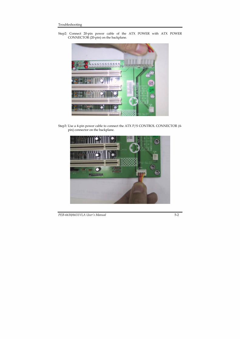
Troubleshooting
PEB-6630/6631VLA User’s Manual 5-2
Step2: Connect 20-pin power cable of the ATX POWER with ATX POWER
CONNECTOR (20-pin) on the backplane.
Step3: Use a 4-pin power cable to connect the ATX P/S CONTROL CONNECTOR (4-
pin) connector on the backplane.

Troubleshooting
PEB-6630/6631VLA User’s Manual 5-3
Step4: Please find the CN14 4-pin ATX Power Control Connector on the near bracket
part of PEB-6630/6631VLA in white color. You will also see a mark with “CN14” on the lower-right side of CN14 header. Connect the 4-pin ATX power control cable with this CN14 header.
Step5: Connect TOGGLE SWITCH with J24 connector on PEB-6630/6631VLA.

Troubleshooting
PEB-6630/6631VLA User’s Manual 5-4
Q: In addition to the above description, is there anything to do to finish up an ATX
system ?? A: Yes. PEB-6630/6631VLA needs to be configured to support ATX function for the
above cabling. Please move jumper JP1 to 3-5 short and 4-6 short (support ATX function).
Q: How can I build up an AT system using ATX power supply A: Do not forget to move JP1 of PEB-6630/6631VLA back to 1-3 short and 2-4 short
(support AT function). If the ATX power supply has a switch, such as ORION-300ATX, do not remove the jumper of backplane connector in step 1, and use the power supply switch as the system power on switch. In all cases, users may apply a 2-pin AT (on/off) switch over pin-3 and pin-4 of the backplane connector in step 1. However, power supply switch needs to be moved to “on”, if there is one.

Troubleshooting
PEB-6630/6631VLA User’s Manual 5-5
5.2 Onboard hardware installation Q: How do I connect my keyboard and mouse ?? A: Users may always adopt PS/2 keyboard and mouse over the PS/2 interface
(through Y-cable), CN8 on PEB-6630/6631VLA.
However, it is also fine to adopt a standard keyboard over the standard keyboard connector on backplane, if provided. In this way, users need to adopt a 5-pin keyboard connection cable to line-up, external keyboard interface, CN10 on PEB-6630/6631VLA with the 5-pin keyboard connector on backplane.
Q: OK. I have finished up hardware installation, but I got nothing when I power on
the system. Why ?? A: There are thousands of different reasons to get this power on failure.
1. Check PEB-6630/6631VLA jumper JP1. For AT power supply or ATX power supply used for AT system, JP1 needs to be at 1-3 and 2-4. Otherwise, it needs to be at 3-5 and 4-6. Incorrect power setting will not allow you to power on the system.
2. Double check if every connector is attached with the correct cable.
3. If you have changed processor with different system clock, please move JP4 (CMOS clear Jumper) to 1-2, power on the system to clear CMOS (move on/off switch from off to on for AT mode, or toggle the switch for ATX mode), power off the system, move JP4 back to 2-3, and power on again.
Q: I connect two IDE devices over one IDE flat cable, but the system either does not
start, or just hangs from time to time. Why ?? A: Make sure that you have configured the two IDE devices as a master and a slave,
respectively. Q: I am using an ATA-66 (or 100) hard drive, how can I know that ATA-66 function
is started?? A: You need to use the 80-pin ATA-66 IDE flat cable to have this function ready.
During POST, you can see ATA-66 (or 100) message while hard drive is being detected.

Troubleshooting
PEB-6630/6631VLA User’s Manual 5-6
5.3 BIOS Setting It is assumed that users have correctly adopted modules and connected all the device cables required before turning on AT power. CPU, CPU fan, CPU fan power cable, 168-pin SDRAM, keyboard, mouse, floppy drive, IDE hard disk, printer, VGA connector, device power cables, ATX accessories or P8/P9 power cable are good examples that deserve attention. With no assurance of properly and correctly accommodating these modules and devices, it is very possible to encounter system failures that result in malfunction of any device. To make sure that you have a successful start with PEB-6630/6631VLA, it is recommended, when going with the boot-up sequence, to hit “DEL” key and enter the BIOS setup menu to tune up a stable BIOS configuration so that you can wake up your system far well. Loading the default optimal setting When prompted with the main setup menu, please scroll down to “Load Optimal Defaults”, press “Enter” and “Y” to load in default optimal BIOS setup. This will force your BIOS setting back to the initial factory configuration. It is recommended to do this so that you can be sure that system is running with the BIOS setting that Portwell has highly endorsed. As a matter of fact, users can load in the default BIOS setting any time system appears to be unstable in boot up sequence. Auto Detect Hard Disks In the BIOS => Standard CMOS setup menu, pick up any one from Primary/Secondary Master/Slave IDE ports, and press “Enter”. Setup the said IDE port and its access mode to “Auto”. This will force system to automatically pick up the IDE devices that are being connected each time system is booted. Improper disable operation There are too many occasions where users disable, in BIOS setup, a certain device/feature in one application, but do not enable it before manipulating with another application where the disabled device is needed. Certainly, users fail to detect this device/feature and end up with system failure. Please check in the BIOS setting that the devices or ports that you need are not disabled. These include the floppy drive, COM1/COM2 ports, parallel port, USB ports, external cache, on-board VGA and Ethernet.

Troubleshooting
PEB-6630/6631VLA User’s Manual 5-7
It is also very common that users would like to disable a certain device/port to release IRQ resource. A few good examples are disable COM1 serial port to release IRQ #4 disable COM2 serial port to release IRQ #3 disable parallel port to release IRQ #7 disable PS/2 mouse to release IRQ #12, …, etc. A quick review of the basic IRQ mapping is given below for your reference.
IRQ# Description IRQ #0 System Counter IRQ #1 Keyboard IRQ #2 Programmed Controller IRQ #3 COM2 IRQ #4 COM1 IRQ #5 Nothing IRQ #6 Floppy Disk Controller IRQ #7 Printer Port (Parallel Port) IRQ #8 CMOS Clock IRQ #9 Nothing IRQ #10 USB interface IRQ #11 Nothing IRQ #12 PS/2 mouse IRQ #13 Data Processor IRQ #14 Primary IDE Controller IRQ #15 Secondary IDE Controller It is then very easy to find out which IRQ resource is ready for additional peripherals. If IRQ resource is not enough, please disable some devices listed above to release more.

Troubleshooting
PEB-6630/6631VLA User’s Manual 5-8
5.4 OS Diagnostics What will be presented here is a brief guide to properly house-in the driver for any Microsoft Windows-95/98/NT device. For other operating systems, please refer to OS manual/guidebook. Booting Users may find quite a lot that Windows-95/98 hangs in loading sequence. Windows logo stays with no progress, or simply no display is given. Please restart your system and hit “F5” when loading the Windows system and enter “Safe mode”. Users will always be allowed to enter “Safe mode” with success to remove devices that are not properly running or installed. Please proceed to do so and restart your Windows. Removed devices will be automatically detected again and drivers will be loaded in if drivers have been copied in the system database, or you will be asked to provide driver source for installation. For Windows-NT 4.0 users, it is always not recommended to change your hardware configuration after your first installation. However, if such a change is needed, please note that sometimes Windows-NT 4.0 will stop loading and prompt you with a whole page of error messages. Please note that reinstallation of this NT hard disk is inevitable. You have to backup your data stored in this hard disk because it is almost impossible to switch back this system unless booting up with another hard disk. If this NT hard disk is installed with FAT16 disk format, please boot up your system with any Windows OS. You will then be able to see this NT hard disk and retrieve any data you have interest in. However, if this NT hard disk is installed with NTFS disk format, there is only NTFS that allows you to retrieve this NT hard disk again. Display setup By default, any Windows OS starts with 640 x 480 by 16 colors display. Please load in the display driver provided in PEB-6630/6631VLA product CDROM to maximize the VGA performance. If you are using a monitor that Windows cannot identify, you will also need to set, in the display setup menu, a system monitor to correctly retrieve display output. For Windows-NT 4.0 users, as PEB-6630/6631VLA provides Direct AGP on-board display feature, Service Pack 3.0 or above is required to activate this display feature.
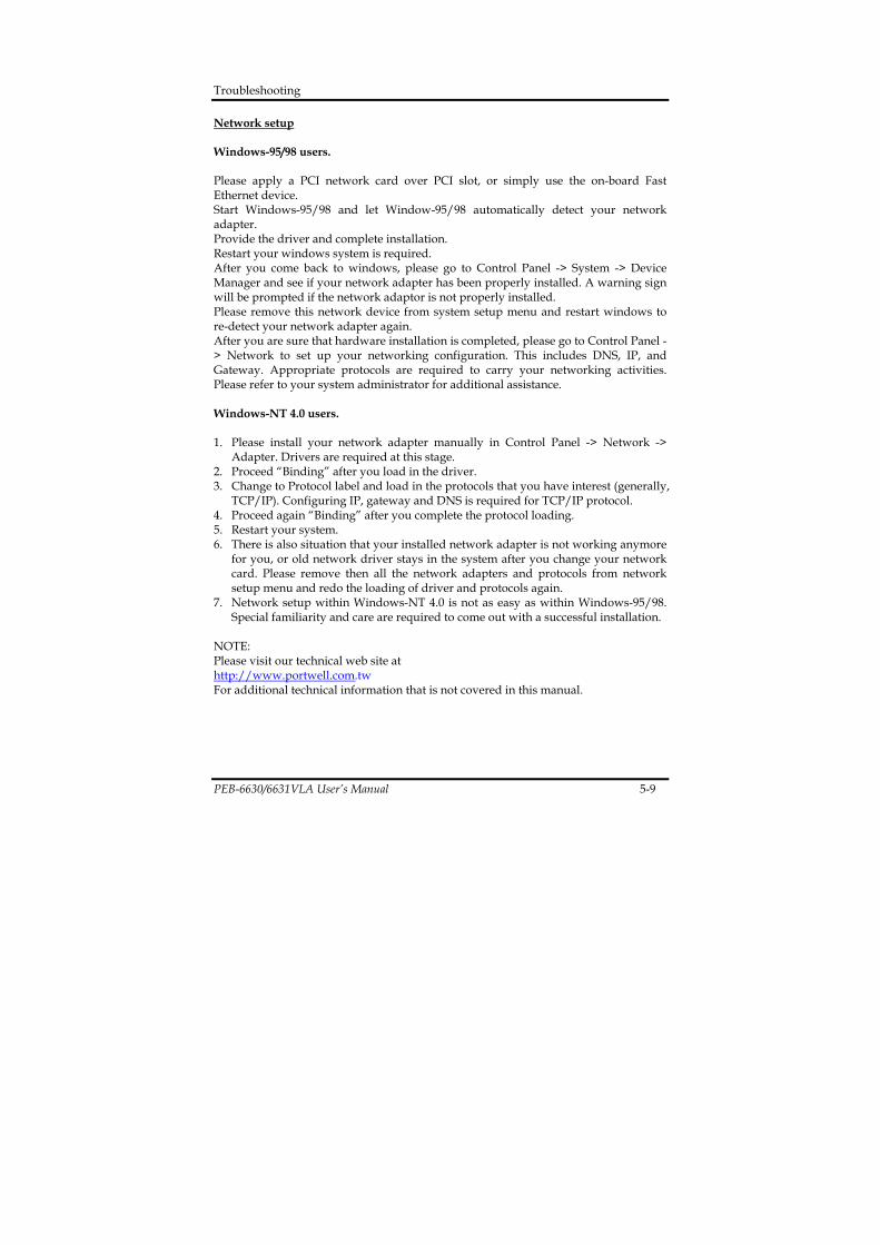
Troubleshooting
PEB-6630/6631VLA User’s Manual 5-9
Network setup Windows-95/98 users. Please apply a PCI network card over PCI slot, or simply use the on-board Fast Ethernet device. Start Windows-95/98 and let Window-95/98 automatically detect your network adapter. Provide the driver and complete installation. Restart your windows system is required. After you come back to windows, please go to Control Panel -> System -> Device Manager and see if your network adapter has been properly installed. A warning sign will be prompted if the network adaptor is not properly installed. Please remove this network device from system setup menu and restart windows to re-detect your network adapter again. After you are sure that hardware installation is completed, please go to Control Panel -> Network to set up your networking configuration. This includes DNS, IP, and Gateway. Appropriate protocols are required to carry your networking activities. Please refer to your system administrator for additional assistance. Windows-NT 4.0 users. 1. Please install your network adapter manually in Control Panel -> Network ->
Adapter. Drivers are required at this stage. 2. Proceed “Binding” after you load in the driver. 3. Change to Protocol label and load in the protocols that you have interest (generally,
TCP/IP). Configuring IP, gateway and DNS is required for TCP/IP protocol. 4. Proceed again “Binding” after you complete the protocol loading. 5. Restart your system. 6. There is also situation that your installed network adapter is not working anymore
for you, or old network driver stays in the system after you change your network card. Please remove then all the network adapters and protocols from network setup menu and redo the loading of driver and protocols again.
7. Network setup within Windows-NT 4.0 is not as easy as within Windows-95/98. Special familiarity and care are required to come out with a successful installation.
NOTE: Please visit our technical web site at http://www.portwell.com.tw For additional technical information that is not covered in this manual.