Embed Size (px)
Citation preview

Audio Serial Interface
(TDM, I2S, LJ)
PLL and Clock Generation
Hardware Pin Control
InterfaceMICBIAS, Regulators and Voltage
Reference
Configurable Digital Filters,
and DRE
Quad Channel ADC with
Front-End DRE Amplifier
IN1P
IN1M
IN2P
IN2M
IN3P
IN3M
IN4P
IN4M
MICBIAS
VREF
FSYNC
BCLK
SDOUT
MSZ
SHDNZ
FMT0
FMT1
MD0
MD1
AREG DREG AVSSThermal Pad
(VSS)AVDD IOVDD
Product
Folder
Order
Now
Technical
Documents
Tools &
Software
Support &Community
An IMPORTANT NOTICE at the end of this data sheet addresses availability, warranty, changes, use in safety-critical applications,intellectual property matters and other important disclaimers. PRODUCTION DATA.
PCM1840SBAS989 –APRIL 2019
PCM1840 Quad Channel, 32-Bit, 192-kHz, Burr-BrownTM Audio ADC
1
1 Features1• Multichannel high-performance ADC:
– 4-channel analog microphones or line-in• ADC line and microphone differential input
performance:– Dynamic range:
– 123-dB, dynamic range enhancer enabled– 113-dB, dynamic range enhancer disabled
– THD+N: –98 dB• ADC differential 2-VRMS full-scale input• ADC sample rate (fS) = 8 kHz to 192 kHz• Hardware pin control configurations• Linear-phase or low-latency filter selection• Flexible audio serial data interface:
– Master or slave interface selection– 32-bits, 4-channel TDM– 32-bits, 2-channel TDM– 32-bits, 2-channel I2S– 32-bits, 2-channel left-justified (LJ)
• Automatic power-down upon loss of audio clocks• Integrated high-performance audio PLL• Low-noise MICBIAS 2.75-V output• Single-supply operation: 3.3 V• I/O-supply operation: 3.3 V or 1.8 V• Power consumption for 3.3-V AVDD supply:
– 17.0 mW/channel at 16-kHz sample rate– 18.4 mW/channel at 48-kHz sample rate
2 Applications• Smart speakers• DVD recorders and players• AV receivers• Video conference systems• IP network cameras
3 DescriptionThe PCM1840 is a high-performance, Burr-Brown™audio analog-to-digital converter (ADC) that supportssimultaneous sampling of up to four analog channels.The device supports differential line and microphoneinputs with 2-VRMS full-scale signal. The deviceintegrates microphone bias voltage, a phase-lockedloop (PLL), a DC removal high-pass filter (HPF), andsupports sample rates up to 192 kHz. The devicesupports time-division multiplexing (TDM), I2S, or left-justified (LJ) audio formats, selectable with thehardware pin level. Additionally, the PCM1840supports master and slave mode selection for theaudio bus interface operation. These integrated high-performance features, along with the ability to bepowered from a single supply of 3.3 V, make thedevice an excellent choice for cost-sensitive, space-constrained audio systems in far-field microphonerecording applications.
The PCM1840 is specified from –40°C to +125°C,and is offered in a 24-pin WQFN package.
Device Information(1)
PART NUMBER PACKAGE BODY SIZE (NOM)
PCM1840 WQFN (24) 4.00 mm × 4.00 mm with0.5-mm pitch
(1) For all available packages, see the package option addendumat the end of the data sheet.
Simplified Block Diagram

2
PCM1840SBAS989 –APRIL 2019 www.ti.com
Product Folder Links: PCM1840
Submit Documentation Feedback Copyright © 2019, Texas Instruments Incorporated
Table of Contents1 Features .................................................................. 12 Applications ........................................................... 13 Description ............................................................. 14 Revision History..................................................... 25 Pin Configuration and Functions ......................... 36 Specifications......................................................... 4
6.1 Absolute Maximum Ratings ...................................... 46.2 ESD Ratings.............................................................. 46.3 Recommended Operating Conditions....................... 46.4 Thermal Information .................................................. 56.5 Electrical Characteristics........................................... 56.6 Timing Requirements: TDM, I2S or LJ Interface....... 76.7 Switching Characteristics: TDM, I2S or LJ Interface. 76.8 Typical Characteristics .............................................. 8
7 Detailed Description ............................................ 107.1 Overview ................................................................. 107.2 Functional Block Diagram ....................................... 10
7.3 Feature Description................................................. 117.4 Device Functional Modes........................................ 26
8 Application and Implementation ........................ 278.1 Application Information............................................ 278.2 Typical Application .................................................. 27
9 Power Supply Recommendations ...................... 3010 Layout................................................................... 31
10.1 Layout Guidelines ................................................. 3110.2 Layout Example .................................................... 31
11 Device and Documentation Support ................. 3211.1 Receiving Notification of Documentation Updates 3211.2 Community Resources.......................................... 3211.3 Trademarks ........................................................... 3211.4 Electrostatic Discharge Caution............................ 3211.5 Glossary ................................................................ 32
12 Mechanical, Packaging, and OrderableInformation ........................................................... 32
4 Revision HistoryNOTE: Page numbers for previous revisions may differ from page numbers in the current version.
DATE REVISION NOTESApril 2020 * Initial release.

24
DR
EG
7IN
1M
1AVDD 18 MD0
23
FS
YN
C8
IN2
P
2AREG 17 MSZ
22
BC
LK
9IN
2M
3VREF 16 FMT0
21
SD
OU
T1
0IN
3P
4AVSS 15 FMT1
20
MD
11
1IN
3M
5MICBIAS 14 SHDNZ
19
IOV
DD
12
IN4
P
6IN1P 13 IN4M
Not to scale
Thermal Pad (VSS)
3
PCM1840www.ti.com SBAS989 –APRIL 2019
Product Folder Links: PCM1840
Submit Documentation FeedbackCopyright © 2019, Texas Instruments Incorporated
5 Pin Configuration and Functions
RTW Package24-Pin WQFN With Exposed Thermal Pad
Top View
Pin FunctionsPIN
TYPE DESCRIPTIONNO. NAME1 AVDD Analog supply Analog power (3.3 V, nominal)2 AREG Analog Supply Analog on-chip regulator output voltage for analog supply (1.8 V, nominal)3 VREF Analog Analog reference voltage filter output4 AVSS Analog supply Analog ground. Short this pin directly to the board ground plane.5 MICBIAS Analog MICBIAS output6 IN1P Analog input Analog input 1P pin7 IN1M Analog input Analog input 1M pin8 IN2P Analog input Analog input 2P pin9 IN2M Analog input Analog input 2M pin10 IN3P Analog input Analog input 3P pin11 IN3M Analog input Analog input 3M pin12 IN4P Analog input Analog input 4P pin13 IN4M Analog input Analog input 4M pin14 SHDNZ Digital input Device hardware shutdown and reset (active low)15 FMT1 Digital input Audio interface format select 1 pin16 FMT0 Digital input Audio interface format select 0 pin17 MSZ Digital input Audio interface bus master or slave select pin18 MD0 Digital input Device configuration mode select 0 pin19 IOVDD Digital supply Digital I/O power supply (1.8 V or 3.3 V, nominal)20 MD1 Digital input Device configuration mode select 1 pin21 SDOUT Digital output Audio serial data interface bus output22 BCLK Digital I/O Audio serial data interface bus bit clock23 FSYNC Digital I/O Audio serial data interface bus frame synchronization signal
4
PCM1840SBAS989 –APRIL 2019 www.ti.com
Product Folder Links: PCM1840
Submit Documentation Feedback Copyright © 2019, Texas Instruments Incorporated
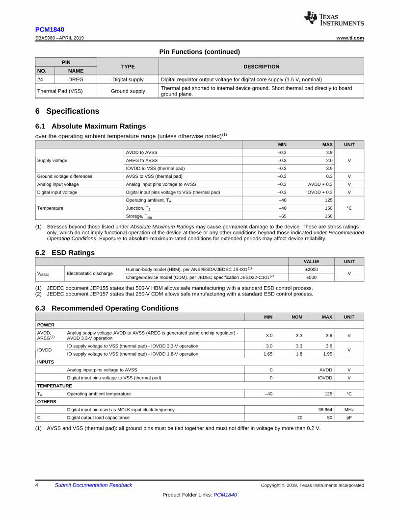
Pin Functions (continued)PIN
TYPE DESCRIPTIONNO. NAME24 DREG Digital supply Digital regulator output voltage for digital core supply (1.5 V, nominal)
Thermal Pad (VSS) Ground supply Thermal pad shorted to internal device ground. Short thermal pad directly to boardground plane.
(1) Stresses beyond those listed under Absolute Maximum Ratings may cause permanent damage to the device. These are stress ratingsonly, which do not imply functional operation of the device at these or any other conditions beyond those indicated under RecommendedOperating Conditions. Exposure to absolute-maximum-rated conditions for extended periods may affect device reliability.
6 Specifications
6.1 Absolute Maximum Ratingsover the operating ambient temperature range (unless otherwise noted) (1)
MIN MAX UNIT
Supply voltage
AVDD to AVSS –0.3 3.9
VAREG to AVSS –0.3 2.0
IOVDD to VSS (thermal pad) –0.3 3.9
Ground voltage differences AVSS to VSS (thermal pad) –0.3 0.3 V
Analog input voltage Analog input pins voltage to AVSS –0.3 AVDD + 0.3 V
Digital input voltage Digital input pins voltage to VSS (thermal pad) –0.3 IOVDD + 0.3 V
Temperature
Operating ambient, TA –40 125
°CJunction, TJ –40 150
Storage, Tstg –65 150
(1) JEDEC document JEP155 states that 500-V HBM allows safe manufacturing with a standard ESD control process.(2) JEDEC document JEP157 states that 250-V CDM allows safe manufacturing with a standard ESD control process.
6.2 ESD RatingsVALUE UNIT
V(ESD) Electrostatic dischargeHuman-body model (HBM), per ANSI/ESDA/JEDEC JS-001 (1) ±2000
VCharged-device model (CDM), per JEDEC specification JESD22-C101 (2) ±500
(1) AVSS and VSS (thermal pad): all ground pins must be tied together and must not differ in voltage by more than 0.2 V.
6.3 Recommended Operating ConditionsMIN NOM MAX UNIT
POWER
AVDD,AREG (1)
Analog supply voltage AVDD to AVSS (AREG is generated using onchip regulator) -AVDD 3.3-V operation 3.0 3.3 3.6 V
IOVDDIO supply voltage to VSS (thermal pad) - IOVDD 3.3-V operation 3.0 3.3 3.6
VIO supply voltage to VSS (thermal pad) - IOVDD 1.8-V operation 1.65 1.8 1.95
INPUTS
Analog input pins voltage to AVSS 0 AVDD V
Digital input pins voltage to VSS (thermal pad) 0 IOVDD V
TEMPERATURE
TA Operating ambient temperature –40 125 °C
OTHERS
Digital input pin used as MCLK input clock frequency 36.864 MHz
CL Digital output load capacitance 20 50 pF
5
PCM1840www.ti.com SBAS989 –APRIL 2019
Product Folder Links: PCM1840
Submit Documentation FeedbackCopyright © 2019, Texas Instruments Incorporated
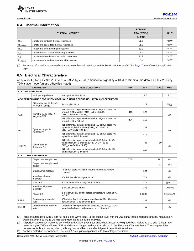
(1) For more information about traditional and new thermal metrics, see the Semiconductor and IC Package Thermal Metrics applicationreport.
6.4 Thermal Information
THERMAL METRIC (1)
PCM1840
UNITRTW (WQFN)
24 PINS
RθJA Junction-to-ambient thermal resistance 32.6 °C/W
RθJC(top) Junction-to-case (top) thermal resistance 25.0 °C/W
RθJB Junction-to-board thermal resistance 11.9 °C/W
ψJT Junction-to-top characterization parameter 0.2 °C/W
ψJB Junction-to-board characterization parameter 11.9 °C/W
RθJC(bot) Junction-to-case (bottom) thermal resistance 2.9 °C/W
(1) Ratio of output level with 1-kHz full-scale sine-wave input, to the output level with the AC signal input shorted to ground, measured A-weighted over a 20-Hz to 20-kHz bandwidth using an audio analyzer.
(2) All performance measurements done with 20-kHz low-pass filter and, where noted, A-weighted filter. Failure to use such a filter mayresult in higher THD and lower SNR and dynamic range readings than shown in the Electrical Characteristics. The low-pass filterremoves out-of-band noise, which, although not audible, may affect dynamic specification values.
(3) For best distortion performance, use input AC-coupling capacitors with low-voltage-coefficient.
6.5 Electrical Characteristicsat TA = 25°C, AVDD = 3.3 V, IOVDD = 3.3 V, fIN = 1-kHz sinusoidal signal, fS = 48 kHz, 32-bit audio data, BCLK = 256 × fS,TDM slave mode (unless otherwise noted)
PARAMETER TEST CONDITIONS MIN TYP MAX UNIT
ADC CONFIGURATION
AC input impedance Input pins INxP or INxM 2.5 kΩ
ADC PERFORMANCE FOR LINE/MICROPHONE INPUT RECORDING : AVDD 3.3-V OPERATION
Differential input full-scaleAC signal voltage AC-coupled input 2 VRMS
SNR Signal-to-noise ratio, A-weighted (1) (2)
IN1 differential input selected and AC signal shorted toground, DRE enabled (DRE_LVL = –36 dB,DRE_MAXGAIN = 24 dB)
115 122dB
IN1 differential input selected and AC signal shorted toground, DRE disabled 106 112
DR Dynamic range, A-weighted (2)
IN1 differential input selected and –60-dB full-scale ACsignal input, DRE enabled (DRE_LVL = –36 dB,DRE_MAXGAIN = 24 dB)
123dB
IN1 differential input selected and –60-dB full-scale ACsignal input, DRE disabled 113
THD+N Total harmonicdistortion (2) (3)
IN1 differential input selected and –1-dB full-scale ACsignal input, DRE enabled (DRE_LVL = –36 dB,DRE_MAXGAIN = 24 dB)
–98 –80dB
IN1 differential input selected and –1-dB full-scale ACsignal input, DRE disabled –98
ADC OTHER PARAMETERS
Output data sample rate 7.35 192 kHz
Output data sample wordlength 32 Bits
Interchannel isolation –1-dB full-scale AC-signal input to non measurementchannel –124 dB
Interchannel gainmismatch –6-dB full-scale AC-signal input 0.1 dB
Gain drift across temperature range 15°C to 35°C –4.4 ppm/°C
Interchannel phasemismatch 1-kHz sinusoidal signal 0.02 Degrees
Phase drift 1-kHz sinusoidal signal, across temperature range 15°Cto 35°C 0.0005 Degrees/°C
PSRR Power-supply rejectionratio
100-mVPP, 1-kHz sinusoidal signal on AVDD, differentialinput selected, 0-dB channel gain 102 dB
CMRR Common-mode rejectionratio
Differential microphone input selected, 100-mVPP, 1-kHzsignal on both pins and measure level at output 60 dB

6
PCM1840SBAS989 –APRIL 2019 www.ti.com
Product Folder Links: PCM1840
Submit Documentation Feedback Copyright © 2019, Texas Instruments Incorporated
Electrical Characteristics (continued)at TA = 25°C, AVDD = 3.3 V, IOVDD = 3.3 V, fIN = 1-kHz sinusoidal signal, fS = 48 kHz, 32-bit audio data, BCLK = 256 × fS,TDM slave mode (unless otherwise noted)
PARAMETER TEST CONDITIONS MIN TYP MAX UNIT
MICROPHONE BIAS
MICBIAS noise BW = 20 Hz to 20 kHz, A-weighted, 1-μF capacitorbetween MICBIAS and AVSS 1.6 µVRMS
MICBIAS voltage VREF V
MICBIAS current drive 20 mA
MICBIAS load regulation Measured up to max load 0.1 0.6 1.8 %
MICBIAS over currentprotection threshold 30 mA
DIGITAL I/O
VILLow-level digital input logicvoltage threshold
All digital pins, IOVDD 1.8-V operation –0.3 0.30 ×IOVDD V
All digital pins, IOVDD 3.3-V operation –0.3 0.8
VIHHigh-level digital input logicvoltage threshold
All digital pins, IOVDD 1.8-V operation 0.7 ×IOVDD
IOVDD +0.3
VAll digital pins, IOVDD 3.3-V operation 2.1 IOVDD +
0.3
VOLLow-level digital outputvoltage
All digital pins, IOL = –2 mA, IOVDD 1.8-V operation 0.45V
All digital pins, IOL = –2 mA, IOVDD 3.3-V operation 0.4
VOHHigh-level digital outputvoltage
All digital pins, IOH = 2 mA, IOVDD 1.8-V operation IOVDD –0.45 V
All digital pins, IOH = 2 mA, IOVDD 3.3-V operation 2.4
IIHInput logic-high leakage fordigital inputs All digital pins, input = IOVDD –5 0.1 5 µA
IILInput logic-low leakage fordigital inputs All digital pins, input = 0 V –5 0.1 5 µA
CINInput capacitance fordigital inputs All digital pins 5 pF
RPD
Pulldown resistance fordigital I/O pins whenasserted on
20 kΩ
TYPICAL SUPPLY CURRENT CONSUMPTION
IAVDDCurrent consumption inhardware shutdown mode
SHDNZ = 0, AVDD = 3.3 V, internal AREG 0.5
µAIIOVDD SHDNZ = 0, all external clocks stopped, IOVDD = 3.3 V 0.1
IIOVDD SHDNZ = 0, all external clocks stopped, IOVDD = 1.8 V 0.1
IAVDD Current consumption withADC 4-channel operatingat fS 16-kHz, BCLK = 256× fS and DRE disable
AVDD = 3.3 V, internal AREG 20.6
mAIIOVDD IOVDD = 3.3 V 0.05
IIOVDD IOVDD = 1.8 V 0.02
IAVDD Current consumption withADC 4-channel operatingat fS 48-kHz, BCLK = 256× fS and DRE disable
AVDD = 3.3 V, internal AREG 22.3
mAIIOVDD IOVDD = 3.3 V 0.1
IIOVDD IOVDD = 1.8 V 0.05
IAVDD Current consumption withADC 4-channel operatingat fS 48-kHz, BCLK = 256× fS and DRE enable
AVDD = 3.3 V, internal AREG 24.4
mAIIOVDD IOVDD = 3.3 V 0.1
IIOVDD IOVDD = 1.8 V 0.05

FSYNC
BCLK
tH(BCLK)
tL(BCLK)
tr(BCLK) tf(BCLK)
tSU(FSYNC)tHLD(FSYNC)
td(SDOUT-FSYNC)td(SDOUT-BCLK)
SDOUT
t(BCLK)
td(FSYNC)
7
PCM1840www.ti.com SBAS989 –APRIL 2019
Product Folder Links: PCM1840
Submit Documentation FeedbackCopyright © 2019, Texas Instruments Incorporated
(1) The BCLK minimum high or low pulse duration must be higher than 25 ns (to meet the timing specifications), if the SDOUT data line islatched on the opposite BCLK edge polarity than the edge used by the device to transmit SDOUT data.
6.6 Timing Requirements: TDM, I2S or LJ Interfaceat TA = 25°C, IOVDD = 3.3 V or 1.8 V and 20-pF load on all outputs (unless otherwise noted); see Figure 3 for timing diagram
MIN NOM MAX UNIT
t(BCLK) BCLK period 40 ns
tH(BCLK) BCLK high pulse duration (1) 18 ns
tL(BCLK) BCLK low pulse duration (1) 18 ns
tSU(FSYNC) FSYNC setup time 8 ns
tHLD(FSYNC) FSYNC hold time 8 ns
tr(BCLK) BCLK rise time 10% - 90% rise time 10 ns
tf(BCLK) BCLK fall time 90% - 10% fall time 10 ns
(1) The BCLK output clock frequency must be lower than 18.5 MHz (to meet the timing specifications), if the SDOUT data line is latched onthe opposite BCLK edge polarity than the edge used by the device to transmit SDOUT data.
6.7 Switching Characteristics: TDM, I2S or LJ Interfaceat TA = 25°C, IOVDD = 3.3 V or 1.8 V and 20-pF load on all outputs (unless otherwise noted); see Figure 3 for timing diagram
PARAMETER TEST CONDITIONS MIN TYP MAX UNITtd(SDOUT-BCLK) BCLK to SDOUT delay 50% of BCLK to 50% of SDOUT 18 ns
td(SDOUT-FSYNC)
FSYNC to SDOUT delay in TDMor LJ mode (for MSB data withTX_OFFSET = 0)
50% of FSYNC to 50% ofSDOUT 18 ns
f(BCLK)BCLK output clock frequency:master mode (1) 24.576 MHz
tH(BCLK)BCLK high pulse duration:master mode 14 ns
tL(BCLK)BCLK low pulse duration: mastermode 14 ns
td(FSYNC)BCLK to FSYNC delay: mastermode 50% of BCLK to 50% of FSYNC 18 ns
tr(BCLK) BCLK rise time: master mode 10% - 90% rise time 8 nstf(BCLK) BCLK fall time: master mode 90% - 10% fall time 8 ns
Figure 1. TDM, I2S, and LJ Interface Timing Diagram

Frequency (Hz)
PS
RR
(d
B)
20 50 100 500 1000 5000 10000 20000
-130
-120
-110
-100
-90
-80
-70
-60
D106
Frequency (Hz)
Ou
tpu
t A
mp
litu
de (
dB
FS
)
20 30 50 70100 200300 500 1000 2000 5000 1000020000 100000-120
-110
-100
-90
-80
-70
-60
-50
-40
-30
-20
-10
0
10
20
FreqADC6
Channel-1Channel-2Channel-3Channel-4
Frequency (Hz)
TH
D+
N (
dB
FS
)
20 50 100 500 1000 5000 10000 20000
-130
-120
-110
-100
-90
-80
-70
-60
D103
Channel-1 : DRE enabled
Channel-2 : DRE enabled
Channel-3 : DRE enabled
Channel-4 : DRE enabled
Frequency (Hz)
TH
D+
N (
dB
FS
)
20 50 100 500 1000 5000 10000 20000
-130
-120
-110
-100
-90
-80
-70
-60
D410
Channel-1
Channel-2
Channel-3
Channel-4
Input Amplitude (dB)
TH
D+
N (
dB
FS
)
-130 -115 -100 -85 -70 -55 -40 -25 -10 0
-130
-120
-110
-100
-90
-80
-70
-60
THD+D101
Channel-1 : DRE enabled
Channel-2 : DRE enabled
Channel-3 : DRE enabled
Channel-4 : DRE enabled
Input Amplitude (dB)
TH
D+
N (
dB
FS
)
-130 -115 -100 -85 -70 -55 -40 -25 -10 0
-130
-120
-110
-100
-90
-80
-70
-60
THD+D101
Channel-1 : DRE disabled
Channel-2 : DRE disabled
Channel-3 : DRE disabled
Channel-4 : DRE disabled
8
PCM1840SBAS989 –APRIL 2019 www.ti.com
Product Folder Links: PCM1840
Submit Documentation Feedback Copyright © 2019, Texas Instruments Incorporated
6.8 Typical Characteristicsat TA = 25°C, AVDD = 3.3 V, IOVDD = 3.3 V, fIN = 1-kHz sinusoidal signal, fS = 48 kHz, 32-bit audio data, BCLK = 256 × fS,TDM slave mode, PLL on, DRE_LVL = –36 dB, channel gain = 0 dB, and linear phase decimation filter (unless otherwisenoted); all performance measurements are done with a 20-kHz, low-pass filter, and an A-weighted filter
Differential input
Figure 2. THD+N vs Input Amplitude With DRE Enabled
Differential input
Figure 3. THD+N vs Input Amplitude With DRE Disabled
Figure 4. THD+N vs Input Frequency With a –60-dBr Input Figure 5. THD+N vs Input Frequency With a –1-dBr Input
Figure 6. Frequency Response With a –12-dBr InputFigure 7. Power-Supply Rejection Ratio vs Ripple
Frequency With 100-mVPP Amplitude

Frequency (Hz)
Ou
tpu
t A
mp
litu
de
(d
BF
S)
20 50 100 500 1000 5000 10000 20000
-200
-180
-160
-140
-120
-100
-80
-60
-40
-20
0
ADC6
Channel-1 : DRE enabled
Channel-2 : DRE enabled
Channel-3 : DRE enabled
Channel-4 : DRE enabled
Frequency (Hz)
Ou
tpu
t A
mp
litu
de
(d
BF
S)
20 50 100 500 1000 5000 10000 20000
-200
-180
-160
-140
-120
-100
-80
-60
-40
-20
0
ADC6
Channel-1 : DRE disabled
Channel-2 : DRE disabled
Channel-3 : DRE disabled
Channel-4 : DRE disabled
Frequency (Hz)
Ou
tpu
t A
mp
litu
de
(d
BF
S)
20 50 100 500 1000 5000 10000 20000
-200
-180
-160
-140
-120
-100
-80
-60
-40
-20
0
ADC6
Channel-1 : DRE enabled
Channel-2 : DRE enabled
Channel-3 : DRE enabled
Channel-4 : DRE enabled
Frequency (Hz)
Ou
tpu
t A
mp
litu
de
(d
BF
S)
20 50 100 500 1000 5000 10000 20000
-200
-180
-160
-140
-120
-100
-80
-60
-40
-20
0
ADC6
Channel-1 : DRE disabled
Channel-2 : DRE disabled
Channel-3 : DRE disabled
Channel-4 : DRE disabled
9
PCM1840www.ti.com SBAS989 –APRIL 2019
Product Folder Links: PCM1840
Submit Documentation FeedbackCopyright © 2019, Texas Instruments Incorporated
Typical Characteristics (continued)at TA = 25°C, AVDD = 3.3 V, IOVDD = 3.3 V, fIN = 1-kHz sinusoidal signal, fS = 48 kHz, 32-bit audio data, BCLK = 256 × fS,TDM slave mode, PLL on, DRE_LVL = –36 dB, channel gain = 0 dB, and linear phase decimation filter (unless otherwisenoted); all performance measurements are done with a 20-kHz, low-pass filter, and an A-weighted filter
Figure 8. FFT With Idle Input With DRE Enabled Figure 9. FFT With Idle Input With DRE Disabled
Figure 10. FFT With a –60-dBr Input With DRE Enabled Figure 11. FFT With a –60-dBr Input With DRE Disabled
Figure 12. FFT With a –1-dBr Input With DRE Enabled Figure 13. FFT With a –1-dBr Input With DRE Disabled

DRE
Amplifier
ADC
Channel-1Digital Filters
(Linear-Phase and
Low-Latency LPF)
and
Dynamic Range
Enhancer (DRE)Audio Serial
Interface (TDM, I2S, LJ)
Audio Clock
Generation
PLL
(Input Clock
Source - BCLK,
MD1)
Hardware Pin Control Interface
BCLK
FSYNC
SDOUT
IN1M
IN1P
FM
T0
MS
Z
IN2M
IN2P
IN3M
IN3P
IN4M
IN4P
FM
T1
MD
0
DRE
Amplifier
ADC
Channel-2
DRE
Amplifier
ADC
Channel-3
DRE
Amplifier
ADC
Channel-4
Microphone
BiasMICBIAS SHDNZ
Regulators, Current Bias and
Voltage Reference
AV
SS
AV
DD
IOV
DD
DR
EG
VR
EF
Th
erm
al P
ad
(VS
S)
AR
EG
MD
1
10
PCM1840SBAS989 –APRIL 2019 www.ti.com
Product Folder Links: PCM1840
Submit Documentation Feedback Copyright © 2019, Texas Instruments Incorporated
7 Detailed Description
7.1 OverviewThe PCM1840 is a high-performance, low-power, quad-channel, audio analog-to-digital converter (ADC) withflexible audio interface control options. This device is intended for applications in voice-activated systems, AVreceivers, TV and blu-ray players, professional microphones, audio conferencing, portable computing,communication, and entertainment applications. The high dynamic range of the device enables far-field audiorecording with high fidelity. This device integrates a host of features that reduces cost, board space, and powerconsumption in space-constrained, battery-powered, consumer, home, and industrial applications. The devicefeatures are controlled through hardware by pulling pins high or low with resistors or a controller GPIO. ThePCM1808 also supports a power-down and reset function by means of halting the system clock.
The PCM1840 consists of the following blocks and features:• Quad-channel, multibit, high-performance delta-sigma (ΔΣ) ADC• Differential audio inputs with a 2-VRMS full-scale signal• Low-noise, 1.6-µVRMS, microphone bias output• Hardware pin control operation to select the device features• Audio bus serial interface master or slave select option• Audio bus serial interface format select option• Audio bus serial interface supported up to 192 kHz sampling• Slave mode supports dynamic range enhancer (DRE) with 123-dB dynamic range• Slave mode supports decimation filters with linear-phase or low-latency filter selection• Master mode operation supported using system clock of 256 × fS or 512 × fS• Power-down function by means of halting the audio clocks• Integrated high-pass filter (HPF) that removes the dc component of the input signal• Integrated low-jitter phase-locked loop (PLL) supporting a wide range of system clocks• Integrated digital and analog voltage regulators to support single-supply 3.3-V operation
7.2 Functional Block Diagram

2 1 0N-1 N-2 N-1 N-2 N-3 2 1 0 N-1 N-2 N-3 2 1 0
Ch1
(Word Length : 32)
Ch2
(Word Length : 32)Ch3 to Ch4
(Word Length : 32)
2 1 0N-1 N-2
Ch1
(Word Length : 32)
FSYNC
BCLK
SDOUT
nth Sample (n+1)th Sample
11
PCM1840www.ti.com SBAS989 –APRIL 2019
Product Folder Links: PCM1840
Submit Documentation FeedbackCopyright © 2019, Texas Instruments Incorporated
7.3 Feature Description
7.3.1 Hardware ControlThe device supports simple hardware pin controlled options to select specific mode of operation and audiointerface for a given system. The MSZ, MD0, MD1, FMT0, and FMT1 pins allow the device to be controlled byeither pullup or pulldown resistors as well as the GPIO from a digital device.
7.3.2 Audio Serial InterfacesDigital audio data flows between the host processor and the PCM1840 on the digital audio serial interface (ASI),or audio bus. This highly flexible ASI bus includes a TDM mode for multichannel operation, support for I2S or left-justified protocols format, and the pin-selectable master-slave configurability for bus clock lines.
The device supports audio bus master or slave mode of operation using the hardware pin MSZ. In slave mode,FSYNC and BCLK work as input pins whereas in master mode, FSYNC and BCLK work as output pinsgenerated by the device.Table 1 shows the master and slave mode selection using the MSZ pin.
Table 1. Master and Slave Mode SelectionMSZ MASTER AND SLAVE SELECTIONLOW Slave mode of operationHIGH Master ode of operation
The bus protocol TDM, I2S, or left-justified (LJ) format can be selected by using the FMT0 and FMT1 pins. Asshown in Table 2, these modes are all most significant byte (MSB)-first, pulse code modulation (PCM) dataformat, with the output channel data word-length of 32 bits.
Table 2. Audio Serial Interface FormatFMT1 FMT0 AUDIO SERIAL INTERFACE FORMATLOW LOW 4-channel output with time division multiplexing (TDM) modeLOW HIGH 2-channel output with time division multiplexing (TDM) modeHIGH LOW 2-channel output with left-justified (LJ) modeHIGH HIGH 2-channel output with inter IC sound (I2S) mode
7.3.2.1 Time Division Multiplexed Audio (TDM) InterfaceIn TDM mode, also known as DSP mode, the rising edge of FSYNC starts the data transfer with the slot 0 datafirst. Immediately after the slot 0 data transmission, the remaining slot data are transmitted in order. FSYNC andeach data bit (except the MSB of slot 0 when TX_OFFSET equals 0) is transmitted on the rising edge of BCLK.Figure 14 to Figure 17 illustrate the protocol timing for TDM operation with various configurations.
Figure 14. TDM Mode Protocol Timing (FMT0 = LOW) In Slave Mode

2 1 0 N-1 N-2 N-3 1 0
Ch1
(Word Length : 32)
Ch2
(Word Length : 32)
FSYNC
BCLK
SDOUT
nth Sample (64 BCLK Cycles) (n+1)th Sample (64 BCLK Cycles)
0 2 1 0 N-1 N-2 N-3 1 N-10
Ch1
(Word Length : 32)
Ch2
(Word Length : 32)
N-1 N-2 N-3 N-1 N-2 N-3
2 1 0 N-1 N-2 N-3 2 1 0 N-1 N-2 N-3 1 0
Ch1
(Word Length : 32)
Ch2
(Word Length : 32)Ch3 to Ch4
(Word Length : 32)
2 1 0
Ch1
(Word Length : 32)
FSYNC
BCLK
SDOUT
nth Sample ( 128 BCLK Cycles) (n+1)th Sample
0 N-1 N-2 N-3 N-1 N-2 N-3
2 1 0N-1 N-2 N-1 N-2 N-3 2 1 0
Ch1
(Word Length : 32)
Ch2
(Word Length : 32)
2 1 0N-1 N-2
Ch1
(Word Length : 32)
BCLK
SDOUT
nth Sample (n+1)th Sample
FSYNC
12
PCM1840SBAS989 –APRIL 2019 www.ti.com
Product Folder Links: PCM1840
Submit Documentation Feedback Copyright © 2019, Texas Instruments Incorporated
Figure 15. TDM Mode Protocol Timing (FMT0 = HIGH) In Slave Mode
Figure 16. TDM Mode Protocol Timing (FMT0 = LOW) In Master Mode
Figure 17. TDM Mode Protocol Timing (FMT0 = HIGH) In Master Mode
For proper operation of the audio bus in TDM mode, the number of bit clocks per frame must be greater than orequal to the number of active output channels times the 32-bits word length of the output channel data. Thedevice transmits a zero data value on SDOUT for the extra unused bit clock cycles. The device supports FSYNCas a pulse with a 1-cycle-wide bit clock, but also supports multiples as well.
7.3.2.2 Inter IC Sound (I2S) InterfaceThe standard I2S protocol is defined for only two channels: left and right. In I2S mode, the MSB of the left slot 0 istransmitted on the falling edge of BCLK in the second cycle after the falling edge of FSYNC. The MSB of theright slot 0 is transmitted on the falling edge of BCLK in the second cycle after the rising edge of FSYNC. Eachsubsequent data bit is transmitted on the falling edge of BCLK. In master mode, FSYNC is transmitted on therising edge of BCLK. Figure 18 and Figure 19 illustrate the protocol timing for I2S operation in slave and mastermode of operation.

1 0N-1 N-2
Left (Ch1)
Slot-0
(Word Length : 32)
1 0N-1 N-2
BCLK
SDOUT
nth Sample (n+1)th Sample
1 0N-1
Right (Ch2)
Slot-0
(Word Length : 32)
Left (Ch1)
Slot-0
(Word Length : 32)
FSYNC
N-2
1 0N-1 N-2
BCLK
SDOUT
nth Sample (64 BCLK Cycles) (n+1)th Sample (64 BCLK Cycles)
1 0N-1
FSYNC
N-21 0 1 0N-1 N-2 1 0N-1 N-2
Left (Ch1)
Slot-0
(Word Length : 32)
Right (Ch2)
Slot-0
(Word Length : 32)
Left (Ch1)
Slot-0
(Word Length : 32)
Right (Ch2)
Slot-0
(Word Length : 32)
1 0N-1 N-2 1 0N-1 N-2
BCLK
SDOUT
nth Sample (n+1)th Sample
1 0N-1
FSYNC
N-2
Left (Ch1)
Slot-0
(Word Length : 32)
Right (Ch2)
Slot-0
(Word Length : 32)
Left (Ch1)
Slot-0
(Word Length : 32)
13
PCM1840www.ti.com SBAS989 –APRIL 2019
Product Folder Links: PCM1840
Submit Documentation FeedbackCopyright © 2019, Texas Instruments Incorporated
Figure 18. I2S Mode Protocol Timing in Slave Mode
Figure 19. I2S Protocol Timing In Master Mode
For proper operation of the audio bus in I2S mode, the number of bit clocks per frame must be greater than orequal to the number of active output channels (including left and right slots) times the 32-bits word length of theoutput channel data. The device FSYNC low pulse must be a number of BCLK cycles wide that is greater than orequal to the number of active left slots times the 32-bits data word length. Similarly, the FSYNC high pulse mustbe a number of BCLK cycles wide that is greater than or equal to the number of active right slots times the 32-bits data word length. The device transmit zero data value on SDOUT for the extra unused bit clock cycles.
7.3.2.3 Left-Justified (LJ) InterfaceThe standard LJ protocol is defined for only two channels: left and right. In LJ mode, the MSB of the left slot 0 istransmitted in the same BCLK cycle after the rising edge of FSYNC. Each subsequent data bit is transmitted onthe falling edge of BCLK. The MSB of the right slot 0 is transmitted in the same BCLK cycle after the falling edgeof FSYNC. Each subsequent data bit is transmitted on the falling edge of BCLK. In master mode, FSYNC istransmitted on the rising edge of BCLK. Figure 20 and Figure 21 illustrate the protocol timing for LJ operation inslave and master mode of operation.
Figure 20. LJ Mode Protocol Timing In Slave Mode

1 0N-1 N-2
Left (Ch1)
Slot-0
(Word Length : 32)
1 0N-1 N-2
BCLK
SDOUT
nth Sample (128 BCLK Cycles) (n+1)th Sample
1 0N-1
Right (Ch2)
Slot-0
(Word Length : 32)
Left (Ch1)
Slot-0
(Word Length : 32)
FSYNC
N-2
14
PCM1840SBAS989 –APRIL 2019 www.ti.com
Product Folder Links: PCM1840
Submit Documentation Feedback Copyright © 2019, Texas Instruments Incorporated
Figure 21. LJ Mode Protocol Timing In Master Mode
For proper operation of the audio bus in LJ mode, the number of bit clocks per frame must be greater than orequal to the number of active output channels (including left and right slots) times the 32-bits word length of theoutput channel data. The device FSYNC high pulse must be a number of BCLK cycles wide that is greater thanor equal to the number of active left slots times the 32-bits data word length. Similarly, the FSYNC low pulsemust be number of BCLK cycles wide that is greater than or equal to the number of active right slots times the32-bits data word length. The device transmit zero data value on SDOUT for the extra unused bit clock cycles.
15
PCM1840www.ti.com SBAS989 –APRIL 2019
Product Folder Links: PCM1840
Submit Documentation FeedbackCopyright © 2019, Texas Instruments Incorporated
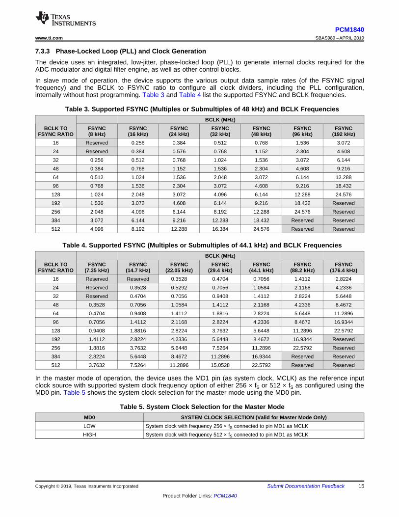
7.3.3 Phase-Locked Loop (PLL) and Clock GenerationThe device uses an integrated, low-jitter, phase-locked loop (PLL) to generate internal clocks required for theADC modulator and digital filter engine, as well as other control blocks.
In slave mode of operation, the device supports the various output data sample rates (of the FSYNC signalfrequency) and the BCLK to FSYNC ratio to configure all clock dividers, including the PLL configuration,internally without host programming. Table 3 and Table 4 list the supported FSYNC and BCLK frequencies.
Table 3. Supported FSYNC (Multiples or Submultiples of 48 kHz) and BCLK Frequencies
BCLK TOFSYNC RATIO
BCLK (MHz)FSYNC(8 kHz)
FSYNC(16 kHz)
FSYNC(24 kHz)
FSYNC(32 kHz)
FSYNC(48 kHz)
FSYNC(96 kHz)
FSYNC(192 kHz)
16 Reserved 0.256 0.384 0.512 0.768 1.536 3.07224 Reserved 0.384 0.576 0.768 1.152 2.304 4.60832 0.256 0.512 0.768 1.024 1.536 3.072 6.14448 0.384 0.768 1.152 1.536 2.304 4.608 9.21664 0.512 1.024 1.536 2.048 3.072 6.144 12.28896 0.768 1.536 2.304 3.072 4.608 9.216 18.432128 1.024 2.048 3.072 4.096 6.144 12.288 24.576192 1.536 3.072 4.608 6.144 9.216 18.432 Reserved256 2.048 4.096 6.144 8.192 12.288 24.576 Reserved384 3.072 6.144 9.216 12.288 18.432 Reserved Reserved512 4.096 8.192 12.288 16.384 24.576 Reserved Reserved
Table 4. Supported FSYNC (Multiples or Submultiples of 44.1 kHz) and BCLK Frequencies
BCLK TOFSYNC RATIO
BCLK (MHz)FSYNC
(7.35 kHz)FSYNC
(14.7 kHz)FSYNC
(22.05 kHz)FSYNC
(29.4 kHz)FSYNC
(44.1 kHz)FSYNC
(88.2 kHz)FSYNC
(176.4 kHz)16 Reserved Reserved 0.3528 0.4704 0.7056 1.4112 2.822424 Reserved 0.3528 0.5292 0.7056 1.0584 2.1168 4.233632 Reserved 0.4704 0.7056 0.9408 1.4112 2.8224 5.644848 0.3528 0.7056 1.0584 1.4112 2.1168 4.2336 8.467264 0.4704 0.9408 1.4112 1.8816 2.8224 5.6448 11.289696 0.7056 1.4112 2.1168 2.8224 4.2336 8.4672 16.9344128 0.9408 1.8816 2.8224 3.7632 5.6448 11.2896 22.5792192 1.4112 2.8224 4.2336 5.6448 8.4672 16.9344 Reserved256 1.8816 3.7632 5.6448 7.5264 11.2896 22.5792 Reserved384 2.8224 5.6448 8.4672 11.2896 16.9344 Reserved Reserved512 3.7632 7.5264 11.2896 15.0528 22.5792 Reserved Reserved
In the master mode of operation, the device uses the MD1 pin (as system clock, MCLK) as the reference inputclock source with supported system clock frequency option of either 256 × fS or 512 × fS as configured using theMD0 pin. Table 5 shows the system clock selection for the master mode using the MD0 pin.
Table 5. System Clock Selection for the Master ModeMD0 SYSTEM CLOCK SELECTION (Valid for Master Mode Only)LOW System clock with frequency 256 × fS connected to pin MD1 as MCLKHIGH System clock with frequency 512 × fS connected to pin MD1 as MCLK

16
PCM1840SBAS989 –APRIL 2019 www.ti.com
Product Folder Links: PCM1840
Submit Documentation Feedback Copyright © 2019, Texas Instruments Incorporated
See Table 7 and Table 20 for the MD0 and MD1 pin function in the slave mode of operation.
7.3.4 Input Channel ConfigurationsThe device consists of four pairs of analog input pins (INxP and INxM) as differential inputs for the recordingchannel. The device supports simultaneous recording of up to four channels using the high-performancemultichannel ADC. The input source for the analog pins can be from electret condenser analog microphones,micro electrical-mechanical system (MEMS) analog microphones, or line-in (auxiliary) inputs from the systemboard.
The voice or audio signal inputs must be capacitively coupled (AC-coupled) to the device and for best distortionperformance, use the low-voltage coefficient capacitors for AC coupling. The device has the typical inputimpedance on INxP or INxM as 2.5 kΩ on each pins. The value of the coupling capacitor in AC-coupled modemust be chosen so that the high-pass filter formed by the coupling capacitor and the input impedance do notaffect the signal content. Before proper recording can begin, this coupling capacitor must be charged up to thecommon-mode voltage at power-up. To enable quick charging, the device has quick charge scheme to speed upthe charging of the coupling capacitor at power-up. The default value of the quick-charge timing is set for acoupling capacitor up to 1 µF.
7.3.5 Reference VoltageAll audio data converters require a DC reference voltage. The PCM1840 achieves low-noise performance byinternally generating a low-noise reference voltage. This reference voltage is generated using a band-gap circuitwith high PSRR performance. This audio converter reference voltage must be filtered externally using a minimum1-µF capacitor connected from the VREF pin to analog ground (AVSS). The value of this reference voltage,VREF, is set to 2.75 V, which in turn supports a 2-VRMS differential full-scale input to the device. The requiredminimum AVDD voltage for this VREF voltage is 3 V. Do not connect any external load to a VREF pin.
7.3.6 Microphone BiasThe device integrates a built-in, low-noise, 1.6-µVRMS microphone bias pin with an output voltage of 2.75 V thatcan be used in the system for biasing electret-condenser microphones or providing the supply to the MEMSanalog or digital microphone. The integrated bias amplifier supports up to 20 mA of load current that can be usedfor multiple microphones and is designed to provide a combination of high PSRR, and low noise bias voltages tobias microphone for high-end audio applications. When using this MICBIAS pin for biasing or supplying tomultiple microphones, avoid any common impedance on the board layout for the MICBIAS connection tominimize coupling across microphones.
Normalized Frequency (1/fS)
Magn
itude
(dB
)
5E-5 0.0001 0.0005 0.001 0.005 0.01 0.05-24
-21
-18
-15
-12
-9
-6
-3
0
3
DPlo
HPF -3 dB Cutoff = 0.00025 u fS
DRE
Amplifier ADC
Configurable
Decimation
Filters
HPFDRE
INP
INM
Output
Channel
Data to
Audio Bus
17
PCM1840www.ti.com SBAS989 –APRIL 2019
Product Folder Links: PCM1840
Submit Documentation FeedbackCopyright © 2019, Texas Instruments Incorporated
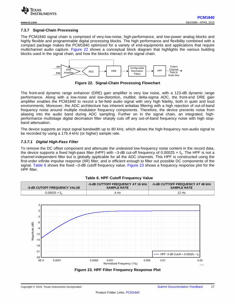
7.3.7 Signal-Chain ProcessingThe PCM1840 signal chain is comprised of very-low-noise, high-performance, and low-power analog blocks andhighly flexible and programmable digital processing blocks. The high performance and flexibility combined with acompact package makes the PCM1840 optimized for a variety of end-equipments and applications that requiremultichannel audio capture. Figure 22 shows a conceptual block diagram that highlights the various buildingblocks used in the signal chain, and how the blocks interact in the signal chain.
Figure 22. Signal-Chain Processing Flowchart
The front-end dynamic range enhancer (DRE) gain amplifier is very low noise, with a 123-dB dynamic rangeperformance. Along with a low-noise and low-distortion, multibit, delta-sigma ADC, the front-end DRE gainamplifier enables the PCM1840 to record a far-field audio signal with very high fidelity, both in quiet and loudenvironments. Moreover, the ADC architecture has inherent antialias filtering with a high rejection of out-of-bandfrequency noise around multiple modulator frequency components. Therefore, the device prevents noise fromaliasing into the audio band during ADC sampling. Further on in the signal chain, an integrated, high-performance multistage digital decimation filter sharply cuts off any out-of-band frequency noise with high stop-band attenuation.
The device supports an input signal bandwidth up to 80 kHz, which allows the high-frequency non-audio signal tobe recorded by using a 176.4-kHz (or higher) sample rate.
7.3.7.1 Digital High-Pass FilterTo remove the DC offset component and attenuate the undesired low-frequency noise content in the record data,the device supports a fixed high-pass filter (HPF) with –3-dB cut-off frequency of 0.00025 × fS. The HPF is not achannel-independent filter but is globally applicable for all the ADC channels. This HPF is constructed using thefirst-order infinite impulse response (IIR) filter, and is efficient enough to filter out possible DC components of thesignal. Table 6 shows the fixed –3-dB cutoff frequency value. Figure 23 shows a frequency response plot for theHPF filter.
Table 6. HPF Cutoff Frequency Value
-3-dB CUTOFF FREQUENCY VALUE-3-dB CUTTOFF FREQUENCY AT 16 kHz
SAMPLE RATE-3-dB CUTTOFF FREQUENCY AT 48 kHz
SAMPLE RATE0.00025 × fS 4 Hz 12 Hz
Figure 23. HPF Filter Frequency Response Plot

Normalized Frequency (1/fS)
Magnitude (
dB
)
0 0.4 0.8 1.2 1.6 2 2.4 2.8 3.2 3.6 4-110
-100
-90
-80
-70
-60
-50
-40
-30
-20
-10
0
10
D001Normalized Frequency (1/fS)
Magnitude (
dB
)
0 0.05 0.1 0.15 0.2 0.25 0.3 0.35 0.4 0.45 0.5-0.5
-0.4
-0.3
-0.2
-0.1
0
0.1
0.2
0.3
0.4
0.5
D001
18
PCM1840SBAS989 –APRIL 2019 www.ti.com
Product Folder Links: PCM1840
Submit Documentation Feedback Copyright © 2019, Texas Instruments Incorporated
7.3.7.2 Configurable Digital Decimation FiltersThe device record channel includes a high dynamic range, built-in digital decimation filter to process theoversampled data from the multibit delta-sigma (ΔΣ) modulator to generate digital data at the same Nyquistsampling rate as the FSYNC rate. The decimation filter can be chosen from two different types only in slavemode, depending on the required frequency response, group delay, and phase linearity requirements for thetarget application. The selection of the decimation filter option can be done by the MD0 pin. Table 7 shows thedecimation filter mode selection for the record channel.
Table 7. Decimation Filter Mode Selection for the Record ChannelMD0 DECIMATION FILTER MODE SELECTION (Supported Only in Slave Mode)LOW Linear phase filters are used for the decimation in slave mode. For master mode, the device
always use linear phase filters for the decimation.HIGH Low latency filters are used for the decimation in slave mode. For master mode, the device
always use linear phase filters for the decimation.
7.3.7.2.1 Linear Phase Filters
The linear phase decimation filters are the default filters set by the device and can be used for all applicationsthat require a perfect linear phase with zero-phase deviation within the pass-band specification of the filter. Thefilter performance specifications and various plots for all supported output sampling rates are listed in thissection.
7.3.7.2.1.1 Sampling Rate: 8 kHz or 7.35 kHz
Figure 24 and Figure 25 respectively show the magnitude response and the pass-band ripple for a decimationfilter with a sampling rate of 8 kHz or 7.35 kHz. Table 8 lists the specifications for a decimation filter with an8-kHz or 7.35-kHz sampling rate.
Figure 24. Linear Phase Decimation Filter MagnitudeResponse
Figure 25. Linear Phase Decimation Filter Pass-BandRipple
Table 8. Linear Phase Decimation Filter SpecificationsPARAMETER TEST CONDITIONS MIN TYP MAX UNIT
Pass-band ripple Frequency range is 0 to 0.454 × fS –0.05 0.05 dB
Stop-band attenuationFrequency range is 0.58 × fS to 4 × fS 72.7
dBFrequency range is 4 × fS onwards 81.2
Group delay or latency Frequency range is 0 to 0.454 × fS 17.1 1/fS

Normalized Frequency (1/fS)
Magnitude (
dB
)
0 0.4 0.8 1.2 1.6 2 2.4 2.8 3.2 3.6 4-110
-100
-90
-80
-70
-60
-50
-40
-30
-20
-10
0
10
D001Normalized Frequency (1/fS)
Magnitude (
dB
)
0 0.05 0.1 0.15 0.2 0.25 0.3 0.35 0.4 0.45 0.5-0.5
-0.4
-0.3
-0.2
-0.1
0
0.1
0.2
0.3
0.4
0.5
D001
Normalized Frequency (1/fS)
Magnitude (
dB
)
0 0.4 0.8 1.2 1.6 2 2.4 2.8 3.2 3.6 4-110
-100
-90
-80
-70
-60
-50
-40
-30
-20
-10
0
10
D001Normalized Frequency (1/fS)
Magnitude (
dB
)
0 0.05 0.1 0.15 0.2 0.25 0.3 0.35 0.4 0.45 0.5-0.5
-0.4
-0.3
-0.2
-0.1
0
0.1
0.2
0.3
0.4
0.5
D001
19
PCM1840www.ti.com SBAS989 –APRIL 2019
Product Folder Links: PCM1840
Submit Documentation FeedbackCopyright © 2019, Texas Instruments Incorporated
7.3.7.2.1.2 Sampling Rate: 16 kHz or 14.7 kHz
Figure 26 and Figure 27 respectively show the magnitude response and the pass-band ripple for a decimationfilter with a sampling rate of 16 kHz or 14.7 kHz. Table 9 lists the specifications for a decimation filter with an 16-kHz or 14.7-kHz sampling rate.
Figure 26. Linear Phase Decimation Filter MagnitudeResponse
Figure 27. Linear Phase Decimation Filter Pass-BandRipple
Table 9. Linear Phase Decimation Filter SpecificationsPARAMETER TEST CONDITIONS MIN TYP MAX UNIT
Pass-band ripple Frequency range is 0 to 0.454 × fS –0.05 0.05 dB
Stop-band attenuationFrequency range is 0.58 × fS to 4 × fS 73.3
dBFrequency range is 4 × fS onwards 95.0
Group delay or latency Frequency range is 0 to 0.454 × fS 15.7 1/fS
7.3.7.2.1.3 Sampling Rate: 24 kHz or 22.05 kHz
Figure 28 and Figure 29 respectively show the magnitude response and the pass-band ripple for a decimationfilter with a sampling rate of 24 kHz or 22.05 kHz. Table 10 lists the specifications for a decimation filter with an24-kHz or 22.05-kHz sampling rate.
Figure 28. Linear Phase Decimation Filter MagnitudeResponse
Figure 29. Linear Phase Decimation Filter Pass-BandRipple
Table 10. Linear Phase Decimation Filter SpecificationsPARAMETER TEST CONDITIONS MIN TYP MAX UNIT
Pass-band ripple Frequency range is 0 to 0.454 × fS –0.05 0.05 dB
Stop-band attenuationFrequency range is 0.58 × fS to 4 × fS 73.0
dBFrequency range is 4 × fS onwards 96.4
Group delay or latency Frequency range is 0 to 0.454 × fS 16.6 1/fS

Normalized Frequency (1/fS)
Magnitude (
dB
)
0 0.4 0.8 1.2 1.6 2 2.4 2.8 3.2 3.6 4-110
-100
-90
-80
-70
-60
-50
-40
-30
-20
-10
0
10
D001Normalized Frequency (1/fS)
Magnitude (
dB
)
0 0.05 0.1 0.15 0.2 0.25 0.3 0.35 0.4 0.45 0.5-0.5
-0.4
-0.3
-0.2
-0.1
0
0.1
0.2
0.3
0.4
0.5
D001
Normalized Frequency (1/fS)
Magnitude (
dB
)
0 0.4 0.8 1.2 1.6 2 2.4 2.8 3.2 3.6 4-110
-100
-90
-80
-70
-60
-50
-40
-30
-20
-10
0
10
D001Normalized Frequency (1/fS)
Magnitude (
dB
)
0 0.05 0.1 0.15 0.2 0.25 0.3 0.35 0.4 0.45 0.5-0.5
-0.4
-0.3
-0.2
-0.1
0
0.1
0.2
0.3
0.4
0.5
D001
20
PCM1840SBAS989 –APRIL 2019 www.ti.com
Product Folder Links: PCM1840
Submit Documentation Feedback Copyright © 2019, Texas Instruments Incorporated
7.3.7.2.1.4 Sampling Rate: 32 kHz or 29.4 kHz
Figure 30 and Figure 31 respectively show the magnitude response and the pass-band ripple for a decimationfilter with a sampling rate of 32 kHz or 29.4 kHz. Table 11 lists the specifications for a decimation filter with an32-kHz or 29.4-kHz sampling rate.
Figure 30. Linear Phase Decimation Filter MagnitudeResponse
Figure 31. Linear Phase Decimation Filter Pass-BandRipple
Table 11. Linear Phase Decimation Filter SpecificationsPARAMETER TEST CONDITIONS MIN TYP MAX UNIT
Pass-band ripple Frequency range is 0 to 0.454 × fS –0.05 0.05 dB
Stop-band attenuationFrequency range is 0.58 × fS to 4 × fS 73.7
dBFrequency range is 4 × fS onwards 107.2
Group delay or latency Frequency range is 0 to 0.454 × fS 16.9 1/fS
7.3.7.2.1.5 Sampling Rate: 48 kHz or 44.1 kHz
Figure 32 and Figure 33 respectively show the magnitude response and the pass-band ripple for a decimationfilter with a sampling rate of 48 kHz or 44.1 kHz. Table 12 lists the specifications for a decimation filter with an48-kHz or 44.1-kHz sampling rate.
Figure 32. Linear Phase Decimation Filter MagnitudeResponse
Figure 33. Linear Phase Decimation Filter Pass-BandRipple
Table 12. Linear Phase Decimation Filter SpecificationsPARAMETER TEST CONDITIONS MIN TYP MAX UNIT
Pass-band ripple Frequency range is 0 to 0.454 × fS –0.05 0.05 dB
Stop-band attenuationFrequency range is 0.58 × fS to 4 × fS 73.8
dBFrequency range is 4 × fS onwards 98.1
Group delay or latency Frequency range is 0 to 0.454 × fS 17.1 1/fS

Normalized Frequency (1/fS)
Magnitude (
dB
)
0 0.4 0.8 1.2 1.6 2 2.4 2.8 3.2 3.6 4-110
-100
-90
-80
-70
-60
-50
-40
-30
-20
-10
0
10
D001Normalized Frequency (1/fS)
Magnitude (
dB
)
0 0.05 0.1 0.15 0.2 0.25 0.3 0.35 0.4-0.5
-0.4
-0.3
-0.2
-0.1
0
0.1
0.2
0.3
0.4
0.5
D001
Normalized Frequency (1/fS)
Magnitude (
dB
)
0 0.4 0.8 1.2 1.6 2 2.4 2.8 3.2 3.6 4-110
-100
-90
-80
-70
-60
-50
-40
-30
-20
-10
0
10
D001Normalized Frequency (1/fS)
Magnitude (
dB
)
0 0.05 0.1 0.15 0.2 0.25 0.3 0.35 0.4 0.45 0.5-0.5
-0.4
-0.3
-0.2
-0.1
0
0.1
0.2
0.3
0.4
0.5
D001
21
PCM1840www.ti.com SBAS989 –APRIL 2019
Product Folder Links: PCM1840
Submit Documentation FeedbackCopyright © 2019, Texas Instruments Incorporated
7.3.7.2.1.6 Sampling Rate: 96 kHz or 88.2 kHz
Figure 34 and Figure 35 respectively show the magnitude response and the pass-band ripple for a decimationfilter with a sampling rate of 96 kHz or 88.2 kHz. Table 13 lists the specifications for a decimation filter with an96-kHz or 88.2-kHz sampling rate.
Figure 34. Linear Phase Decimation Filter MagnitudeResponse
Figure 35. Linear Phase Decimation Filter Pass-BandRipple
Table 13. Linear Phase Decimation Filter SpecificationsPARAMETER TEST CONDITIONS MIN TYP MAX UNIT
Pass-band ripple Frequency range is 0 to 0.454 × fS –0.05 0.05 dB
Stop-band attenuationFrequency range is 0.58 × fS to 4 × fS 73.6
dBFrequency range is 4 × fS onwards 97.9
Group delay or latency Frequency range is 0 to 0.454 × fS 17.1 1/fS
7.3.7.2.1.7 Sampling Rate: 192 kHz or 176.4 kHz
Figure 36 and Figure 37 respectively show the magnitude response and the pass-band ripple for a decimationfilter with a sampling rate of 192 kHz or 176.4 kHz. Table 14 lists the specifications for a decimation filter with an192-kHz or 176.4-kHz sampling rate.
Figure 36. Linear Phase Decimation Filter MagnitudeResponse
Figure 37. Linear Phase Decimation Filter Pass-BandRipple
Table 14. Linear Phase Decimation Filter SpecificationsPARAMETER TEST CONDITIONS MIN TYP MAX UNIT
Pass-band ripple Frequency range is 0 to 0.3 × fS –0.05 0.05 dB
Stop-band attenuationFrequency range is 0.473 × fS to 4 × fS 70.0
dBFrequency range is 4 × fS onwards 111.0
Group delay or latency Frequency range is 0 to 0.3 × fS 11.9 1/fS

Normalized Frequency (1/fS)
Magn
itude
(dB
)
0 0.4 0.8 1.2 1.6 2 2.4 2.8 3.2 3.6 4-110
-100
-90
-80
-70
-60
-50
-40
-30
-20
-10
0
10
D002
Normalized Frequency (1/fS)
Magnitude (
dB
)
Phase D
evia
tion fro
m L
inear
(Degre
e)
0 0.05 0.1 0.15 0.2 0.25 0.3 0.35 0.4 0.45 0.5-0.5 -0.5
-0.4 -0.4
-0.3 -0.3
-0.2 -0.2
-0.1 -0.1
0 0
0.1 0.1
0.2 0.2
0.3 0.3
0.4 0.4
0.5 0.5
D002
Pass-Band RipplePhase Deviation
22
PCM1840SBAS989 –APRIL 2019 www.ti.com
Product Folder Links: PCM1840
Submit Documentation Feedback Copyright © 2019, Texas Instruments Incorporated
7.3.7.2.2 Low-Latency Filters
For applications where low latency with minimal phase deviation (within the audio band) is critical, the low-latency decimation filters on the PCM1840 can be used. The device supports these filters with a group delay ofapproximately seven samples with an almost linear phase response within the 0.365 × fS frequency band. Thissection provides the filter performance specifications and various plots for all supported output sampling rates forthe low-latency filters.
7.3.7.2.2.1 Sampling Rate: 16 kHz or 14.7 kHz
Figure 38 shows the magnitude response and Figure 39 shows the pass-band ripple and phase deviation for adecimation filter with a sampling rate of 16 kHz or 14.7 kHz. Table 15 lists the specifications for a decimationfilter with a 16-kHz or 14.7-kHz sampling rate.
Figure 38. Low-Latency Decimation Filter MagnitudeResponse
Figure 39. Low-Latency Decimation Filter Pass-BandRipple and Phase Deviation
Table 15. Low-Latency Decimation Filter SpecificationsPARAMETER TEST CONDITIONS MIN TYP MAX UNIT
Pass-band ripple Frequency range is 0 to 0.451 × fS –0.05 0.05 dBStop-band attenuation Frequency range is 0.61 × fS onwards 87.3 dBGroup delay or latency Frequency range is 0 to 0.363 × fS 7.6 1/fSGroup delay deviation Frequency range is 0 to 0.363 × fS –0.022 0.022 1/fSPhase deviation Frequency range is 0 to 0.363 × fS –0.21 0.25 Degrees

Normalized Frequency (1/fS)
Magn
itude
(dB
)
0 0.4 0.8 1.2 1.6 2 2.4 2.8 3.2 3.6 4-110
-100
-90
-80
-70
-60
-50
-40
-30
-20
-10
0
10
D002
Normalized Frequency (1/fS)
Magnitude (
dB
)
Phase D
evia
tion fro
m L
inear
(Degre
e)
0 0.05 0.1 0.15 0.2 0.25 0.3 0.35 0.4 0.45 0.5-0.5 -0.5
-0.4 -0.4
-0.3 -0.3
-0.2 -0.2
-0.1 -0.1
0 0
0.1 0.1
0.2 0.2
0.3 0.3
0.4 0.4
0.5 0.5
D002
Pass-Band RipplePhase Deviation
Normalized Frequency (1/fS)
Magn
itude
(dB
)
0 0.4 0.8 1.2 1.6 2 2.4 2.8 3.2 3.6 4-110
-100
-90
-80
-70
-60
-50
-40
-30
-20
-10
0
10
D002
Normalized Frequency (1/fS)
Magnitude (
dB
)
Phase D
evia
tion fro
m L
inear
(Degre
e)
0 0.05 0.1 0.15 0.2 0.25 0.3 0.35 0.4 0.45 0.5-0.5 -0.5
-0.4 -0.4
-0.3 -0.3
-0.2 -0.2
-0.1 -0.1
0 0
0.1 0.1
0.2 0.2
0.3 0.3
0.4 0.4
0.5 0.5
D002
Pass-Band RipplePhase Deviation
23
PCM1840www.ti.com SBAS989 –APRIL 2019
Product Folder Links: PCM1840
Submit Documentation FeedbackCopyright © 2019, Texas Instruments Incorporated
7.3.7.2.2.2 Sampling Rate: 24 kHz or 22.05 kHz
Figure 40 shows the magnitude response and Figure 41 shows the pass-band ripple and phase deviation for adecimation filter with a sampling rate of 24 kHz or 22.05 kHz. Table 16 lists the specifications for a decimationfilter with a 24-kHz or 22.05-kHz sampling rate.
Figure 40. Low-Latency Decimation Filter MagnitudeResponse
Figure 41. Low-Latency Decimation Filter Pass-BandRipple and Phase Deviation
Table 16. Low-Latency Decimation Filter SpecificationsPARAMETER TEST CONDITIONS MIN TYP MAX UNIT
Pass-band ripple Frequency range is 0 to 0.459 × fS –0.01 0.01 dBStop-band attenuation Frequency range is 0.6 × fS onwards 87.2 dBGroup delay or latency Frequency range is 0 to 0.365 × fS 7.5 1/fSGroup delay deviation Frequency range is 0 to 0.365 × fS –0.026 0.026 1/fSPhase deviation Frequency range is 0 to 0.365 × fS –0.26 0.30 Degrees
7.3.7.2.2.3 Sampling Rate: 32 kHz or 29.4 kHz
Figure 42 shows the magnitude response and Figure 43 shows the pass-band ripple and phase deviation for adecimation filter with a sampling rate of 32 kHz or 29.4 kHz. Table 17 lists the specifications for a decimationfilter with a 32-kHz or 29.4-kHz sampling rate.
Figure 42. Low-Latency Decimation Filter MagnitudeResponse
Figure 43. Low-Latency Decimation Filter Pass-BandRipple and Phase Deviation

Normalized Frequency (1/fS)
Magn
itude
(dB
)
0 0.4 0.8 1.2 1.6 2 2.4 2.8 3.2 3.6 4-110
-100
-90
-80
-70
-60
-50
-40
-30
-20
-10
0
10
D002
Normalized Frequency (1/fS)
Magnitude (
dB
)
Phase D
evia
tion fro
m L
inear
(Degre
e)
0 0.05 0.1 0.15 0.2 0.25 0.3 0.35 0.4 0.45 0.5-0.5 -0.5
-0.4 -0.4
-0.3 -0.3
-0.2 -0.2
-0.1 -0.1
0 0
0.1 0.1
0.2 0.2
0.3 0.3
0.4 0.4
0.5 0.5
D002
Pass-Band RipplePhase Deviation
24
PCM1840SBAS989 –APRIL 2019 www.ti.com
Product Folder Links: PCM1840
Submit Documentation Feedback Copyright © 2019, Texas Instruments Incorporated
Table 17. Low-Latency Decimation Filter SpecificationsPARAMETER TEST CONDITIONS MIN TYP MAX UNIT
Pass-band ripple Frequency range is 0 to 0.457 × fS –0.04 0.04 dBStop-band attenuation Frequency range is 0.6 × fS onwards 88.3 dBGroup delay or latency Frequency range is 0 to 0.368 × fS 8.7 1/fSGroup delay deviation Frequency range is 0 to 0.368 × fS –0.026 0.026 1/fSPhase deviation Frequency range is 0 to 0.368 × fS –0.26 0.31 Degrees
7.3.7.2.2.4 Sampling Rate: 48 kHz or 44.1 kHz
Figure 44 shows the magnitude response and Figure 45 shows the pass-band ripple and phase deviation for adecimation filter with a sampling rate of 48 kHz or 44.1 kHz. Table 18 lists the specifications for a decimationfilter with a 48-kHz or 44.1-kHz sampling rate.
Figure 44. Low-Latency Decimation Filter MagnitudeResponse
Figure 45. Low-Latency Decimation Filter Pass-BandRipple and Phase Deviation
Table 18. Low-Latency Decimation Filter SpecificationsPARAMETER TEST CONDITIONS MIN TYP MAX UNIT
Pass-band ripple Frequency range is 0 to 0.452 × fS –0.015 0.015 dBStop-band attenuation Frequency range is 0.6 × fS onwards 86.4 dBGroup delay or latency Frequency range is 0 to 0.365 × fS 7.7 1/fSGroup delay deviation Frequency range is 0 to 0.365 × fS –0.027 0.027 1/fSPhase deviation Frequency range is 0 to 0.365 × fS –0.25 0.30 Degrees
Normalized Frequency (1/fS)
Magn
itude
(dB
)
0 0.4 0.8 1.2 1.6 2 2.4 2.8 3.2 3.6 4-110
-100
-90
-80
-70
-60
-50
-40
-30
-20
-10
0
10
D002
Normalized Frequency (1/fS)
Magnitude (
dB
)
Phase D
evia
tion fro
m L
inear
(Degre
e)
0 0.05 0.1 0.15 0.2 0.25 0.3 0.35 0.4 0.45 0.5-0.5 -0.5
-0.4 -0.4
-0.3 -0.3
-0.2 -0.2
-0.1 -0.1
0 0
0.1 0.1
0.2 0.2
0.3 0.3
0.4 0.4
0.5 0.5
D002
Pass-Band RipplePhase Deviation
25
PCM1840www.ti.com SBAS989 –APRIL 2019
Product Folder Links: PCM1840
Submit Documentation FeedbackCopyright © 2019, Texas Instruments Incorporated
7.3.7.2.2.5 Sampling Rate: 96 kHz or 88.2 kHz
Figure 46 shows the magnitude response and Figure 47 shows the pass-band ripple and phase deviation for adecimation filter with a sampling rate of 96 kHz or 88.2 kHz. Table 19 lists the specifications for a decimationfilter with a 96-kHz or 88.2-kHz sampling rate.
Figure 46. Low-Latency Decimation Filter MagnitudeResponse
Figure 47. Low-Latency Decimation Filter Pass-BandRipple and Phase Deviation
Table 19. Low-Latency Decimation Filter SpecificationsPARAMETER TEST CONDITIONS MIN TYP MAX UNIT
Pass-band ripple Frequency range is 0 to 0.466 × fS –0.04 0.04 dBStop-band attenuation Frequency range is 0.6 × fS onwards 86.3 dBGroup delay or latency Frequency range is 0 to 0.365 × fS 7.7 1/fSGroup delay deviation Frequency range is 0 to 0.365 × fS –0.027 0.027 1/fSPhase deviation Frequency range is 0 to 0.365 × fS –0.26 0.30 Degrees

26
PCM1840SBAS989 –APRIL 2019 www.ti.com
Product Folder Links: PCM1840
Submit Documentation Feedback Copyright © 2019, Texas Instruments Incorporated
7.3.8 Dynamic Range Enhancer (DRE)The device integrates an ultra-low noise front-end DRE gain amplifier with 123-dB dynamic range performancewith a low-noise, low-distortion, multibit delta-sigma (ΔΣ) ADC with a 108-dB dynamic range. The dynamic rangeenhancer (DRE) is a digitally assisted algorithm to boost the overall channel performance. The DRE monitors theincoming signal amplitude and accordingly adjusts the internal DRE amplifier gain automatically. The DREachieves a complete-channel dynamic range as high as 123 dB. At a system level, the DRE scheme enables far-field, high-fidelity recording of audio signals in very quiet environments and low-distortion recording in loudenvironments.
The DRE can be enable only in slave mode by driving high to the MD1 pin. Table 20 shows the DRE selectionfor the record channel.
Table 20. DRE Selection for the Record ChannelMD1 DRE SELECTION (Supported Only in Slave Mode)LOW DRE is disabled in slave mode. For master mode, DRE is always disabled.HIGH DRE is enabled with DRE_LVL = –36 dB and DRE_MAXGAIN = 24 dB in slave mode. For
master mode, DRE is always disabled.
This algorithm is implemented with very low latency and all signal chain blocks are designed to minimize anyaudible artifacts that may occur resulting from dynamic gain modulation. The target signal threshold level,DRE_LVL, at which DRE is triggered is fixed to the –36-dB input signal level. The DRE gain range can bedynamically modulated by using DRE_MAXGAIN, which is fixed to 24 dB to maximize the benefit of the DRE inreal-world applications and to minimize any audible artifacts.
Enabling the DRE for processing increases the power consumption of the device because of increased signalprocessing. Therefore, disable the DRE for low-power critical applications. Furthermore, the DRE is notsupported for output sample rates greater than 48 kHz.
7.4 Device Functional Modes
7.4.1 Hardware ShutdownThe device enters hardware shutdown mode when the SHDNZ pin is asserted low or the AVDD supply voltage isnot applied to the device. In hardware shutdown mode, the device consumes the minimum quiescent currentfrom the AVDD supply. If the SHDNZ pin is asserted low when the device is in active mode, the device rampsdown volume on the record data, powers down the analog and digital blocks, and puts the device into hardwareshutdown mode in 25 ms (typical).
7.4.2 Active ModeIn the hardware shutdown state, when the SHDNZ pin goes high, the device starts the internal boot-up sequenceand then enters into active mode in less than 20 ms (typical). Assert the SHDNZ pin high only when the IOVDDsupply settles to a steady voltage level and all hardware control pins (MSZ, MD0, MD1, FMT0, and FMT1) aredriven to the voltage level for the device desired mode of operation.
In active mode, when the audio clocks are available, the device powers up all the ADC channels and startstransmitting the data over the audio serial interface. If the clocks are stopped then the device auto powers downthe ADC channels.

1 F
1 F
1 F
1 F
1 F
1 F
1 F
1 F
3.3 V
(3.0 V to 3.6 V)
OR
1.8 V
(1.65 V to 1.95 V)
3.3 V
(3.0 V to
3.6 V)
PCM1840
IN1P
IN1M
GND
GND
GND
GND
MIC
BIA
S
AV
SS
VR
EF
GND
1 F
AR
EG
0.1 F
GND
1 F
GND
10 F
AV
DD
1 F
DREG
10 F
GND
0.1 F
0.1 F
IN2P
IN2M
IN3P
IN3M
IN4P
IN4M
Host
Processor
IOVDD
GND
Thermal Pad
(VSS)
GND
SD
OU
T
BC
LK
FS
YN
C
SH
DN
Z
10 F
AMIC1
OUTP
OUTM
VDD
VSS
AMIC2
OUTP
OUTM
VDD
VSS
AMIC3
OUTP
OUTM
VDD
VSS
AMIC4
OUTP
OUTM
VDD
VSS
GND
0.1 F
0.1 F
0.1 F
0.1 F
0.1 F
LOW/HIGH Pin Selector
MD
0
FM
T1
FM
T0
MS
Z
MD
1
27
PCM1840www.ti.com SBAS989 –APRIL 2019
Product Folder Links: PCM1840
Submit Documentation FeedbackCopyright © 2019, Texas Instruments Incorporated
8 Application and Implementation
NOTEInformation in the following applications sections is not part of the TI componentspecification, and TI does not warrant its accuracy or completeness. TI’s customers areresponsible for determining suitability of components for their purposes. Customers shouldvalidate and test their design implementation to confirm system functionality.
8.1 Application InformationThe PCM1840 is a multichannel, high-performance audio analog-to-digital converter (ADC) that supports outputsample rates of up to 192 kHz. The device supports up to four analog microphones for simultaneous recordingapplications.
The PCM1840 configuration is supported using various hardware pin control options. The device supports ahighly flexible, audio serial interface (TDM, I2S, and LJ) to transmit audio data seamlessly in the system acrossdevices.
8.2 Typical ApplicationFigure 48 shows a typical configuration of the PCM1840 for an application using four analog microelectrical-mechanical system (MEMS) microphones for simultaneous recording operation with a time-division multiplexing(TDM) audio data slave interface. For best distortion performance, use input AC-coupling capacitors with a low-voltage coefficient.
Figure 48. Four-Channel Analog Microphone Recording Diagram for 3.3-V AVDD Operation

28
PCM1840SBAS989 –APRIL 2019 www.ti.com
Product Folder Links: PCM1840
Submit Documentation Feedback Copyright © 2019, Texas Instruments Incorporated
Typical Application (continued)8.2.1 Design RequirementsTable 21 lists the design parameters for this application.
Table 21. Design ParametersKEY PARAMETER SPECIFICATION: 3.3-V AVDD OPERATION
AVDD 3.3 VAVDD supply current consumption > 23 mA (PLL on, four-channel recording, fS = 48 kHz)IOVDD 1.8 V or 3.3 VMaximum MICBIAS current 10 mA (MICBIAS voltage is the same as VREF)
8.2.2 Detailed Design ProcedureThis section describes the necessary steps to configure the PCM1840 for this specific application. The followingsteps provide a sequence of items that must be executed in the time between powering the device up andreading data from the device or transitioning from one mode to another mode of operation.1. Apply power to the device:
a. Power-up the IOVDD and AVDD power supplies, keeping the SHDNZ pin voltage lowb. The device now goes into hardware shutdown mode (ultra-low-power mode < 1 µA)
2. Transition from hardware shutdown mode to active mode whenever required for the recording operation:a. Connect the MSZ, FMT0, and FMT1 pins voltage low to configure the device in 4-channel TDM slave
modeb. Release SHDNZ only when the IOVDD and AVDD power supplies settle to the steady-state operating
voltagec. Apply FSYNC and BCLK with the desired output sample rates and the BCLK to FSYNC ratio
This specific step can be done at any point in the sequence after step a
See the Phase-Locked Loop (PLL) and Clock Generation section for supported sample rates and theBCLK to FSYNC ratio
d. The device recording data are now sent to the host processor via the TDM audio serial data bus3. Assert the SHDNZ pin low to enter hardware shutdown mode (again) at any time4. Follow step 2 onwards to exit hardware shutdown mode (again)

Frequency (Hz)
Ou
tpu
t A
mp
litu
de (
dB
FS
)
20 50 100 500 1000 5000 10000 20000
-200
-180
-160
-140
-120
-100
-80
-60
-40
-20
0
D212
Channel-1 : DRE disabled
Channel-2 : DRE disabled
Channel-3 : DRE disabled
Channel-4 : DRE disabled
Input Amplitude (dB)
TH
D+
N (
dB
FS
)
-130 -115 -100 -85 -70 -55 -40 -25 -10 0
-130
-120
-110
-100
-90
-80
-70
-60
THD+D202
Channel-1 : DRE disabled
Channel-2 : DRE disabled
Channel-3 : DRE disabled
Channel-4 : DRE disabled
Frequency (Hz)
Ou
tpu
t A
mp
litu
de (
dB
FS
)
20 50 100 500 1000 5000 10000 20000
-200
-180
-160
-140
-120
-100
-80
-60
-40
-20
0
D212
Channel-1 : DRE enabled
Channel-2 : DRE enabled
Channel-3 : DRE enabled
Channel-4 : DRE enabled
Input Amplitude (dB)
TH
D+
N (
dB
FS
)
-130 -115 -100 -85 -70 -55 -40 -25 -10 0
-130
-120
-110
-100
-90
-80
-70
-60
THD+D202
Channel-1 : DRE enabled
Channel-2 : DRE enabled
Channel-3 : DRE enabled
Channel-4 : DRE enabled
29
PCM1840www.ti.com SBAS989 –APRIL 2019
Product Folder Links: PCM1840
Submit Documentation FeedbackCopyright © 2019, Texas Instruments Incorporated
8.2.3 Application CurvesMeasurements are done on the EVM by feeding the device analog input signal using audio precision and with a3.3-V AVDD supply.
Figure 49. FFT With a –60-dBr Input With DRE Enabled Figure 50. THD+N vs Input Amplitude With DRE Enabled
Figure 51. FFT With a –60-dBr Input With DRE Disabled Figure 52. THD+N vs Input Amplitude With DRE Disabled

AVDD
IOVDD
SHDNZ
t1
t2
t3
t4
30
PCM1840SBAS989 –APRIL 2019 www.ti.com
Product Folder Links: PCM1840
Submit Documentation Feedback Copyright © 2019, Texas Instruments Incorporated
9 Power Supply RecommendationsThe power-supply sequence between the IOVDD and AVDD rails can be applied in any order. However, keepthe SHDNZ pin low until the IOVDD supply voltage settles to a stable and supported operating voltage range.After all supplies are stable, set the SHDNZ pin high to initialize the device. Assert the SHDNZ pin high onlywhen all hardware control pins (MSZ, MD0, MD1, FMT0, and FMT1) are driven to the voltage level for the devicedesired mode of operation.
For the supply power-up requirement, t1 and t2 must be at least 100 µs. For the supply power-down requirement,t3 and t4 must be at least 10 ms. This timing (as shown in Figure 53) allows the device to ramp down the volumeon the record data, power down the analog and digital blocks, and put the device into hardware shutdown mode.
Figure 53. Power-Supply Sequencing Requirement Timing Diagram
Make sure that the supply ramp rate is slower than 1 V/µs and that the wait time between a power-down and apower-up event is at least 100 ms.
The PCM1840 supports a single AVDD supply operation by integrating an on-chip digital regulator, DREG, andan analog regulator, AREG. However, if the AVDD voltage is less than 1.98 V in the system, then short theAREG and AVDD pins onboard.

18 : MD0
17 : MSZ
16 : FMT0
15 : FMT1
14 : SHDNZ
13 : IN4M
12
: I
N4
P
11
: I
N3
M
10
: I
N3
P
9 :
IN
2M
8 :
IN
2P
7 :
IN
1M
6 : IN1P
5 : MICBIAS
4 : AVSS
3 : VREF
2 : AREG
1 : AVDD
19
: I
OV
DD
20
: M
D1
21
: S
DO
UT
22
: B
CL
K
23
: F
SY
NC
24
: D
RE
G
Audio output interface connections
Ha
rdw
are
co
ntr
ol p
ins
Audio input signal connections
Po
we
r co
nn
ectio
ns
31
PCM1840www.ti.com SBAS989 –APRIL 2019
Product Folder Links: PCM1840
Submit Documentation FeedbackCopyright © 2019, Texas Instruments Incorporated
10 Layout
10.1 Layout GuidelinesEach system design and printed circuit board (PCB) layout is unique. The layout must be carefully reviewed inthe context of a specific PCB design. However, the following guidelines can optimize the device performance:• Connect the thermal pad to ground. Use a via pattern to connect the device thermal pad, which is the area
directly under the device, to the ground planes. This connection helps dissipate heat from the device.• The decoupling capacitors for the power supplies must be placed close to the device pins.• Route the analog differential audio signals differentially on the PCB for better noise immunity. Avoid crossing
digital and analog signals to prevent undesirable crosstalk.• The device internal voltage references must be filtered using external capacitors. Place the filter capacitors
near the VREF pin for optimal performance.• Directly tap the MICBIAS pin to avoid common impedance when routing the biasing or supply traces for
multiple microphones to avoid coupling across microphones.• Directly short the VREF and MICBIAS external capacitors ground terminal to the AVSS pin without using any
vias for this connection trace.• Place the MICBIAS capacitor (with low equivalent series resistance) close to the device with minimal trace
impedance.• Use ground planes to provide the lowest impedance for power and signal current between the device and the
decoupling capacitors. Treat the area directly under the device as a central ground area for the device, andall device grounds must be connected directly to that area.
10.2 Layout Example
Figure 54. Example Layout

32
PCM1840SBAS989 –APRIL 2019 www.ti.com
Product Folder Links: PCM1840
Submit Documentation Feedback Copyright © 2019, Texas Instruments Incorporated
11 Device and Documentation Support
11.1 Receiving Notification of Documentation UpdatesTo receive notification of documentation updates, navigate to the device product folder on ti.com. In the upperright corner, click on Alert me to register and receive a weekly digest of any product information that haschanged. For change details, review the revision history included in any revised document.
11.2 Community ResourcesTI E2E™ support forums are an engineer's go-to source for fast, verified answers and design help — straightfrom the experts. Search existing answers or ask your own question to get the quick design help you need.
Linked content is provided "AS IS" by the respective contributors. They do not constitute TI specifications and donot necessarily reflect TI's views; see TI's Terms of Use.
11.3 TrademarksBurr-Brown, E2E are trademarks of Texas Instruments.All other trademarks are the property of their respective owners.
11.4 Electrostatic Discharge CautionThis integrated circuit can be damaged by ESD. Texas Instruments recommends that all integrated circuits be handled withappropriate precautions. Failure to observe proper handling and installation procedures can cause damage.
ESD damage can range from subtle performance degradation to complete device failure. Precision integrated circuits may be moresusceptible to damage because very small parametric changes could cause the device not to meet its published specifications.
11.5 GlossarySLYZ022 — TI Glossary.
This glossary lists and explains terms, acronyms, and definitions.
12 Mechanical, Packaging, and Orderable InformationThe following pages include mechanical, packaging, and orderable information. This information is the mostcurrent data available for the designated devices. This data is subject to change without notice and revision ofthis document. For browser-based versions of this data sheet, refer to the left-hand navigation.
PACKAGE OPTION ADDENDUM
www.ti.com 19-Aug-2021
Addendum-Page 1
PACKAGING INFORMATION
Orderable Device Status(1)
Package Type PackageDrawing
Pins PackageQty
Eco Plan(2)
Lead finish/Ball material
(6)
MSL Peak Temp(3)
Op Temp (°C) Device Marking(4/5)
Samples
PCM1840IRTWR ACTIVE WQFN RTW 24 3000 RoHS & Green NIPDAU Level-1-260C-UNLIM -40 to 125 PCM1840
PCM1840IRTWT ACTIVE WQFN RTW 24 250 RoHS & Green NIPDAU Level-1-260C-UNLIM -40 to 125 PCM1840
(1) The marketing status values are defined as follows:ACTIVE: Product device recommended for new designs.LIFEBUY: TI has announced that the device will be discontinued, and a lifetime-buy period is in effect.NRND: Not recommended for new designs. Device is in production to support existing customers, but TI does not recommend using this part in a new design.PREVIEW: Device has been announced but is not in production. Samples may or may not be available.OBSOLETE: TI has discontinued the production of the device.
(2) RoHS: TI defines "RoHS" to mean semiconductor products that are compliant with the current EU RoHS requirements for all 10 RoHS substances, including the requirement that RoHS substancedo not exceed 0.1% by weight in homogeneous materials. Where designed to be soldered at high temperatures, "RoHS" products are suitable for use in specified lead-free processes. TI mayreference these types of products as "Pb-Free".RoHS Exempt: TI defines "RoHS Exempt" to mean products that contain lead but are compliant with EU RoHS pursuant to a specific EU RoHS exemption.Green: TI defines "Green" to mean the content of Chlorine (Cl) and Bromine (Br) based flame retardants meet JS709B low halogen requirements of <=1000ppm threshold. Antimony trioxide basedflame retardants must also meet the <=1000ppm threshold requirement.
(3) MSL, Peak Temp. - The Moisture Sensitivity Level rating according to the JEDEC industry standard classifications, and peak solder temperature.
(4) There may be additional marking, which relates to the logo, the lot trace code information, or the environmental category on the device.
(5) Multiple Device Markings will be inside parentheses. Only one Device Marking contained in parentheses and separated by a "~" will appear on a device. If a line is indented then it is a continuationof the previous line and the two combined represent the entire Device Marking for that device.
(6) Lead finish/Ball material - Orderable Devices may have multiple material finish options. Finish options are separated by a vertical ruled line. Lead finish/Ball material values may wrap to twolines if the finish value exceeds the maximum column width.
Important Information and Disclaimer:The information provided on this page represents TI's knowledge and belief as of the date that it is provided. TI bases its knowledge and belief on informationprovided by third parties, and makes no representation or warranty as to the accuracy of such information. Efforts are underway to better integrate information from third parties. TI has taken andcontinues to take reasonable steps to provide representative and accurate information but may not have conducted destructive testing or chemical analysis on incoming materials and chemicals.TI and TI suppliers consider certain information to be proprietary, and thus CAS numbers and other limited information may not be available for release.
In no event shall TI's liability arising out of such information exceed the total purchase price of the TI part(s) at issue in this document sold by TI to Customer on an annual basis.

PACKAGE OPTION ADDENDUM
www.ti.com 19-Aug-2021
Addendum-Page 2

TAPE AND REEL INFORMATION
*All dimensions are nominal
Device PackageType
PackageDrawing
Pins SPQ ReelDiameter
(mm)
ReelWidth
W1 (mm)
A0(mm)
B0(mm)
K0(mm)
P1(mm)
W(mm)
Pin1Quadrant
PCM1840IRTWR WQFN RTW 24 3000 330.0 12.4 4.25 4.25 1.15 8.0 12.0 Q2
PCM1840IRTWT WQFN RTW 24 250 180.0 12.4 4.25 4.25 1.15 8.0 12.0 Q2
PACKAGE MATERIALS INFORMATION
www.ti.com 23-Jul-2020
Pack Materials-Page 1

*All dimensions are nominal
Device Package Type Package Drawing Pins SPQ Length (mm) Width (mm) Height (mm)
PCM1840IRTWR WQFN RTW 24 3000 367.0 367.0 35.0
PCM1840IRTWT WQFN RTW 24 250 210.0 185.0 35.0
PACKAGE MATERIALS INFORMATION
www.ti.com 23-Jul-2020
Pack Materials-Page 2


IMPORTANT NOTICE AND DISCLAIMERTI PROVIDES TECHNICAL AND RELIABILITY DATA (INCLUDING DATASHEETS), DESIGN RESOURCES (INCLUDING REFERENCEDESIGNS), APPLICATION OR OTHER DESIGN ADVICE, WEB TOOLS, SAFETY INFORMATION, AND OTHER RESOURCES “AS IS”AND WITH ALL FAULTS, AND DISCLAIMS ALL WARRANTIES, EXPRESS AND IMPLIED, INCLUDING WITHOUT LIMITATION ANYIMPLIED WARRANTIES OF MERCHANTABILITY, FITNESS FOR A PARTICULAR PURPOSE OR NON-INFRINGEMENT OF THIRDPARTY INTELLECTUAL PROPERTY RIGHTS.These resources are intended for skilled developers designing with TI products. You are solely responsible for (1) selecting the appropriateTI products for your application, (2) designing, validating and testing your application, and (3) ensuring your application meets applicablestandards, and any other safety, security, or other requirements. These resources are subject to change without notice. TI grants youpermission to use these resources only for development of an application that uses the TI products described in the resource. Otherreproduction and display of these resources is prohibited. No license is granted to any other TI intellectual property right or to any third partyintellectual property right. TI disclaims responsibility for, and you will fully indemnify TI and its representatives against, any claims, damages,costs, losses, and liabilities arising out of your use of these resources.TI’s products are provided subject to TI’s Terms of Sale (https:www.ti.com/legal/termsofsale.html) or other applicable terms available eitheron ti.com or provided in conjunction with such TI products. TI’s provision of these resources does not expand or otherwise alter TI’sapplicable warranties or warranty disclaimers for TI products.IMPORTANT NOTICE
Mailing Address: Texas Instruments, Post Office Box 655303, Dallas, Texas 75265Copyright © 2021, Texas Instruments Incorporated