Embed Size (px)
Citation preview

Part IA Engineering
Digital Circuits &
Information Processing
Handout 1
Combinational Logic
Richard PragerTim Flack
January 2009
1
Aims
The aims of the course are to:
• Familiarize students with combinational and se-quential digital logic circuits, the analogue-digitalinterface, and the hardware and basic operationof microprocessors, memory and the associatedelectronic circuits which are required to build mi-croprocessor based systems.
• Teach the engineering relevance and applicationof digital and microprocessor-based systems, givestudents the ability to design simple systems ofthis kind, and understand microprocessor opera-tion at the assembly-code level.
2

From Semiconductors to Computers
• build transistors from semiconductors
• build gates from transistors
• build logic functions from gates
• build flip-flop bistables from logic
• build counters and sequencers from flip-flops
• build microprocessors from sequencers
• build computers from microprocessors
3
Contents of Handout 1
Section A Introduction to logic gates.This section covers the materialfor questions 1 and 2 onexamples paper 1.
Section B Building gates from transistors.This section covers the materialfor questions 3 – 6 onexamples paper 1.
Section C Boolean algebra for logic design.Introduction to VHDL.This section covers the materialfor questions 7 – 11 onexamples paper 1.
Section D Karnaugh maps for logic design.This section covers the materialfor questions 1 – 5 onexamples paper 2.
4
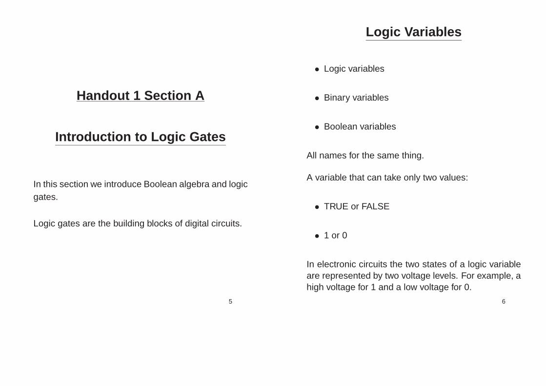
Handout 1 Section A
Introduction to Logic Gates
In this section we introduce Boolean algebra and logicgates.
Logic gates are the building blocks of digital circuits.
5
Logic Variables
• Logic variables
• Binary variables
• Boolean variables
All names for the same thing.
A variable that can take only two values:
• TRUE or FALSE
• 1 or 0
In electronic circuits the two states of a logic variableare represented by two voltage levels. For example, ahigh voltage for 1 and a low voltage for 0.
6

Uses of Simple Logic
Heating Boiler
If chimney not blocked andhouse is cold and pilot light litthen open main fuel valve tostart up boiler.
B = chimney blocked
C = house is cold
P = pilot alight
V = open fuel valve
V = ( NOT B ) AND C AND P
7
Uses of Simple Logic
Washing Machine
If drum not turning and no wa-ter in drum and program fin-ished then permit door to beopened.
T = drum turningW = water in drumP = program activeL = door unlocked
L = ( NOT T ) AND ( NOT W ) AND ( NOT P )
We can write this using bars above the symbols todenote NOT.
L = T AND W AND P
8

Logic Gates
Electronic circuits that have logic signals as their in-puts and outputs are known as LOGIC CIRCUITS orDIGITAL CIRCUITS.
Basic logic circuits with one or more inputs, and oneoutput, are also known as GATES.
GATES are used as building blocks in the design ofmore complex logic circuits.
There are several ways of representing logic functions:
• Graphical symbols used to represent the gates.
• Input-output maps.
• Boolean algebra.
9
NOT Gate
Graphical Input-output BooleanSymbol Map representation
YA1
0
A
1
0
Y = A
A NOT gate is called an ‘inverter’.
Y is TRUE if and only if A is FALSE.
A circle on the output of a gate always implies that itis an inverting output.
10

AND Gate
Graphical Input-output BooleanSymbol Map representation
YA
B
BA
0
1
1
0 0 0
1 0Y = A.B
Y is TRUE if and only if A is TRUE and B is TRUE.
In Boolean algebra AND is represented by a dot .
11
OR Gate
Graphical Input-output BooleanSymbol Map representation
YA
B
BA
0
1
1
0 0
1 1
1
Y = A + B
Y is TRUE if A is TRUE or B is TRUE (or both).
In Boolean algebra OR is representedby a plus sign +
12

EXCLUSIVE OR Gate
Graphical Input-output BooleanSymbol Map representation
BY
A
BA
0
0
1
0 0
1
1
1Y = A ⊕ B
Y is TRUE if A is TRUE or B is TRUE but not both.
In Boolean algebra XOR is represented by an ⊕ sign.
13
NAND Gate
Graphical Input-output BooleanSymbol Map representation
YA
B
BA
0
0
1
0
1
1
1
1
Y = A.B
Y is TRUE if A is FALSE or B is FALSE (or both).
Y is FALSE if and only if A is TRUE and B is TRUE.
14

NOR Gate
Graphical Input-output BooleanSymbol Map representation
YA
B
BA
0
0
1
0
1
1
0 0Y = A + B
Y is TRUE if and only if A is FALSE and B is FALSE.
Y is FALSE if A is TRUE or B is TRUE (or both).
15
Boiler Example
If chimney not blocked and house is cold and pilot lightlit then open main fuel valve to start up boiler.
B = chimney blocked
C = house is cold
P = pilot alight
V = open fuel valve
V = B.C.P
V
B
C
P
16

Washing Machine Example
If drum not turning and no water in drum and programfinished then permit door to be opened.
T = drum turning
W = water in drum
P = program active
L = door unlocked
L = T .W.P
W
T
P
L
17
Handout 1 Section B
Building Gates from Transistors
Logic circuits are non-linear so we first have to learn agraphical technique for analyzing non-linear circuits.
The construction of an NMOS inverter from an N-channelfield effect transistor is described.
We then outline the structure of NMOS AND gatesand OR gates, and estimate the speed of NMOS cir-cuits.
A discussion of the power consumption of NMOS gatesleads to the introduction of the CMOS inverter circuit.
18

Implementing Logic Gates
YA
in
Vout
Invertercircuit
VoutVin
V
V+
0v V+
A high voltage repre-sents logic 1.
A zero voltage repre-sents logic 0.
The graph shows anideal characteristic foran inverter circuit.
Note that it is non-linear.
19
Solving Non-linear Circuits
Ω
2Ω
1
10v
0v
x
Solve a simple circuit graphically.
The same technique will still workwhen we introduce non-linear com-ponents.
of 1 ohm
Characteristic
of 2 ohm resistor
Currentthrough2 ohm
Currentthrough1 ohm
Voltage across
Characteristic
1 ohm
10vVoltage across 2 ohm x0v
20

Ω
0v
1
x
I
10v
Thing
Thingcharacteristic
V
Suppose we now re-place the lower resistorwith a non-linear com-ponent (that we will calla ‘Thing’).
of 1 ohm
Currentthrough1 ohm
Voltage across1 ohm
Characteristicof Thing
CurrentthroughThing Characteristic
Voltage across0vThing
x 10v
21
Thingcharacteristic
1Ω
x
V
I
0v
10v
ThingThe characteristic ofthe upper component isdrawn backwards alongthe V axis, starting atthe supply voltage.
of Thing
Charac
terist
ic
of 1
ohm
Voltage across1 ohm
Voltage acrossThing
CurrentthroughThing
Current
Characteristic
through
x
1 ohm
10v0v
22

Building Gates from Transistors
We start by building logic gates out of N-channel MOS-FETs.
Metal Oxide Semiconductor Field Effect Transistor
Enhancement mode: means off when VGS = 0. Thealternative is a depletion mode transistor which is on(i.e. conducts from drain to source) when VGS = 0.
23
N-channel MOSFET
p-typesubstrate
N-type layer:inversion
Reverse biased
p-n junction
p-typesubstrate
Source
+VD
0v
0v
Silicon dioxide insulator
Gate
Drain
Drain +VD
+V
0v
Gate
Source
ON
OFF
G
D
S
n+
n+
n+
n+
G
24

NMOSFET Characteristics
DS
V VoltsDS
GSV = 0v
GSV = 10v
GSV = 8v
GSV = 6v
GSV = 2vGSV = 4v
I
100
2
4
6
8
10
12
0 2 4 6 8
mA
GSV Volts
IDS
mA
VT
0 3 6
IDS as a function ofVGS at constant VDS
The transistor conductswhen VGS reaches theThreshold voltage: VT
25
NMOS Inverter
Ω
DDV = 10v
VGS
Vin
Vout
VDS
1k
0v
Here is the circuit to imple-ment an inverter using anNMOS FET and a 1kΩ re-sistor.
DS
V VoltsDS
GSV = 0v
GSV = 10v
GSV = 8v
GSV = 6v
GSV = 2vGSV = 4v
I
100
2
4
6
8
10
12
0 2 4 6 8
mA
0
2
I
4
6
8
10
12
0 2 4 6 8
mA
10
V Volts
NMOS FET ResistorCharacteristic Characteristic
26
DS
V VoltsDS
GSV = 0v
GSV = 10v
GSV = 8v
GSV = 6v
GSV = 2vGSV = 4v
I
100
2
4
6
8
10
12
0 2 4 6 8
mA
in
Vout
V10
2
4
6
8
10
0 2 4 6 8
27
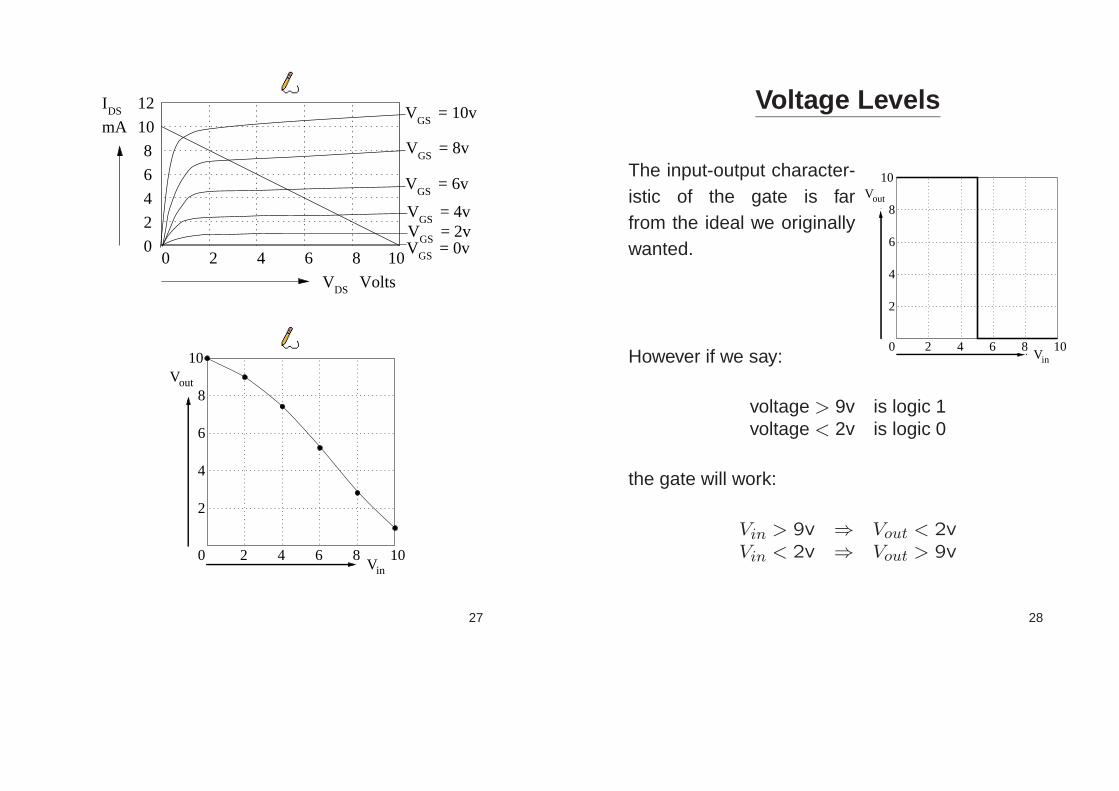
Voltage Levels
in
Vout
V10
2
4
6
8
10
0 2 4 6 8
The input-output character-istic of the gate is farfrom the ideal we originallywanted.
However if we say:
voltage > 9v is logic 1voltage < 2v is logic 0
the gate will work:
Vin > 9v ⇒ Vout < 2vVin < 2v ⇒ Vout > 9v
28

DDV
VY
0v
R
VVA B
What sort of gate is this?Think of the transistors as switches. When VGS ishigh they conduct. Otherwise they don’t conduct.
A B Ylow low high
high low lowlow high low
high high low
This corresponds to a NOR gate: Y = A + B
29
Y
DDV
VA
VB
V
0v
R
A B Ylow low highhigh low highlow high high
high high low
This corresponds to a NAND gate: Y = A.B
30

Benefit of Using Gates
When we have a complicated logic function to imple-ment, (eg. the boiler example previously discussedV = B.C.P ), you don’t have to design a special tran-sistor circuit to provide the functionality.
Instead you just buy an integrated circuit (or chip) thatprovides the appropriate gates.
For the boiler example we would need a three-inputAND gate and an inverter.
31
Speed of NMOS Logic
One of the main speed limitations in real NMOS logicis due to stray capacitance. The output of each gate isconnected by a length of metal track to the input of thenext. This has capacitance to ground. We thereforemodify the circuit model.
Vin
ΩR = 1k
DIIC
DDV = 10v
Vout
IR
0v
C
32

Assume that initially Vin is high, hence Vout = 1 V.
At time t = 0, Vin falls to 0 V, so ID = 0.
IR = IC
VDD − Vout
R= C
dVout
dt
SodVout
dt+
Vout
RC=
VDD
RC
⇒ Vout = VDD + (1 − VDD) exp
(
−t
RC
)
Which means that 95% of the voltage change will takea time of 3RC.
33
Using a FET to replace the Resistor
A big advantage of chips is that they are small.
Implementing a resistor on a chip takes up a lot ofspace on the silicon.
Fortunately it is possible to make a MOSFET behave(almost) like a resistor by connecting the Gate to theDrain. Thus VGS = VDS.
DS
V VoltsDS
GSV = 0v
GSV = 10v
GSV = 8v
GSV = 6v
GSV = 2vGSV = 4v
I
0
2
4
6
8
10
12
0 2 4 6 8
mA
10
It’s not quite a straight line, so behaviour will not bethe exactly same as a resistor. However, it’s roughlylike 900Ω.
34

Smaller NMOS Inverter
Using a FET to approximate a resistor we can producea revised design for an inverter circuit that is easier tominiaturize.
in
Vout
DDV = 10v
Vswitch
0v
pseudo-resistor (load)
35
Power Consumption
Ω
DDV = 10v
Vin
Vout
0v Vin
V
1k
out
10
2
4
6
8
10
0 2 4 6 8
When Vout = 10v there is no current (ID = 0. Thereis therefore no power dissipated.
However, when Vout 6= 10v current will flow downthrough the resistor and heat will be generated.
For example, when Vin = 10v ⇒ Vout = 1v andID = 9mA so 81mW will be dissipated in the resistorand 9mW will be dissipated in the FET.
36
Complementary MOS
The problem with NMOS logic is power dissipation inthe resistors. To solve this, CMOS logic was invented.This uses both NMOSFETS and PMOSFETS.
PMOSFETS are essentially NMOSFETS with all thepolarities reversed:
DS
V VoltsDS
GSV = 0v
GSV = -10v
GSV = -8v
GSV = -6v
GSV = -4v
GSV = -2v
I
-100
0
mA
-12
-10
-8
-6
-4
-2
-2 -4 -6 -8
D
G
D
S
S
G
37
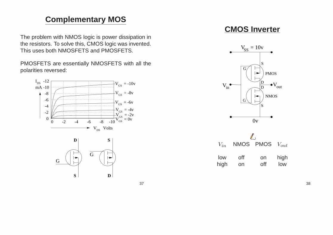
CMOS Inverter
VinVout
V = 10vSS
NMOS
0v
S
S
DD
G
GPMOS
Vin NMOS PMOS Vout
low off on highhigh on off low
38

NMOS Characteristic PMOS CharacteristicDS
V VoltsDS
GSV = 0v
GSV = 10v
GSV = 8v
GSV = 6v
GSV = 2vGSV = 4v
I
100
2
4
6
8
10
12
0 2 4 6 8
mADS
V VoltsDS
GSV = 0v
GSV = -10v
GSV = -8v
GSV = -6v
GSV = -4v
GSV = -2v
I
-100
0
mA
-12
-10
-8
-6
-4
-2
-2 -4 -6 -8
0
2
4
6
V = -10v
8
10
12
0 2 4 6 8 10
Intersection of curves
Voltage across NMOS
mA
I
GSV = 0v
PMOS
NMOS
GS
(a)Vin = 0v ⇒ Vout = 10v. No current flows.
39
GS
NMOSV = 4v
PMOS
GSV = -6v
PMOS
0
2
4
6
8
10
12
0 2 4 6 8 10
mA
I Intersection of curves
Voltage across NMOSVoltage across
(b) Vin = 4v ⇒ Vout = 9.5v, I = 2.7mA.
0 2 4 6 8 10
10
12
0
2
4
6
8
GS
NMOS
NMOSV = 6v
PMOS
GSV = -4v
mA
I Intersection of curves
Voltage across PMOSVoltage across
(c) Vin = 6v ⇒ Vout = 0.5v, I = 2.7mA.
40

V = 0vGS
2
Voltage across PMOS
4
6
8
10
12
0 2 4 6 8 10
Intersection of curves
mA
I
GS
NMOS
PMOS
V = 10v
(d)Vin = 10v ⇒ Vout = 0v. No current flows.
in
Vout
V10
2
4
6
8
10
0 2 4 6 8
Using these values wecan construct the input-output characteristic ofthe inverter circuit. Notethat the CMOS inverteris much closer to ourideal than the NMOSinverter was.
41
Power in CMOS Inverter
Vin I /mA Power /mW
0 0.0 02 1.0 104 2.7 275 3.6 366 2.7 278 1.0 10
10 0.0 0
inV
Power
0 2 4 6 8 10
10
20
30
40
mW
Note that currentonly flows when thegate is changingstate. This meansthat power is onlydissipated as thegate switches on oroff.
42

CMOS NAND Gate
V = 10vSS
AV
VY
VB
0v
T1 T2
T3
T4
VA VB T1 T2 T3 T4 VY
low low on on off off highlow high on off on off highhigh low off on off on highhigh high off off on on low
43
Logic Families
NMOS Compact, slowish, cheap.
CMOS Propagation delay 8–50 nS, max clock frequency12–40 MHz for gates in individual packages. Powerconsumption < 10−6 W/gate when not changing,and about 10−4 W/gate when changing at 100kHz.
TTL Constructed from bipolar transistors. Propaga-tion delay 1.5–10 nS, max clock frequency 35–200 MHz. Power consumption is about 10−2 W/gate.
ECL Constructed from bipolar transistors. High speed.High power consumption; current flows all the time.
44

Handout 1 Section C
Boolean Algebra for Logic Design
In this section we introduce the laws of Boolean al-gebra and show how it can be used to design com-binational logic circuits. We then introduce the hard-ware description language VHDL. This language canbe used to enable computer-aided design of logic cir-cuits.
Combinational logic circuits do not have an internalstored state; the output is a function of the currentinputs. (Later in the course we will study circuits witha stored internal state. These are called sequentiallogic circuits.)
45
Combinational Logic Design
W
T
P
L
In our washing machine ex-ample we needed to imple-ment the logic function
L = T .W.P
This could have been achieved more simply using thefact that
L = T .W.P = (T + W + P)
W
T
P
L
so a single NOR gate will dothe whole job.
46

In an extreme example, it would be very useful to beable to work out that
D
Y
A
B
C
can be replaced by
CY
B
This sort of problem can be solved using Boolean al-gebra and Karnaugh maps.
47
We need:
1. Techniques for simplifying logic expressions. Sim-pler expressions mean fewer gates which lead tolower cost.
2. Techniques for manipulating expressions so thatthe required function can be computed using gatesof only certain types. We thus only need to stocka limited range of gates which can be readily avail-able and cheap.
We are going to study two ways of solving these prob-
lems: Boolean algebra and Karnaugh maps.
Boolean algebra rigorous, computable.
Karnaugh maps visual, exhaustive, copes with up to5 variables.
48

Boolean Algebra
CommutationA + B = B + A normalA.B = B.A normal
Association(A + B) + C = A + (B + C) normal(A.B).C = A.(B.C) normal
DistributionA.(B + C + . . .) = (A.B) + (A.C) + . . . normalA + (B.C. . . .) = (A + B).(A + C). . . . NEW
AbsorptionA + (A.C) = A NEWA.(A + C) = A NEW
49
ORs ANDsA + 0 = A A.0 = 0A + A = A A.A = A
A + 1 = 1 A.1 = A
A + A = 1 A.A = 0
AND takes precedence over OR.For example A.B + C.D = (A.B) + (C.D).
Every Boolean law has a dual: any valid statement is
also valid with
. replaced by ++ replaced by .0 replaced by 11 replaced by 0
50

Show that A.(A + B) = A.B
A.(A + B) = A.A + A.B
= 0 + A.B
= A.B
Show that A + A.B = A + B
A + (A.B) = (A + A).(A + B)
= 1.(A + B)
= A + B
51
Every Variable in Every Term
A useful technique is to expand each term until it in-cludes one instance of each variable (or its compli-ment). It may be possible to simplify the expressionby canceling terms in this expanded form.
If there are two variable (A and B) then terms like A.B
or A.B are fine as they stand because they alreadyinclude all the variables. A term A would need to beexpanded to A.B + A.B.
Here, as an illustration, the technique is used to provethe absorption rule:
A + A.B
= A.B + A.B + A.B
= A52

Simplify X.Y + Y .Z + X.Z + X.Y.Z
= X.Y.Z + X.Y.Z + X.Y.Z + X.Y.Z + X.Y.Z + X.Y.Z
= X.Y + Y.Z + X.Z
= X.Y + Y.Z
X.Y + Y.Z + X.Z + X.Y.Z
( X.Y + X.Y.Z = X.Y )
53
De Morgan’s Theorem
A + B + C + . . . = A.B.C. . . .
A.B.C. . . . = A + B + C + . . .
A + B + C + . . . = A.B.C. . . .
A.B.C. . . . = A + B + C + . . .
In a simple expression like A+B+C (or A.B.C) youcan change all the operators from OR to AND (or viceversa) provided you put a bar over each term individ-ually and a further bar over the whole expression.
54

Proof of De Morgan’s Theorem
For two variables we can prove A + B = A.B andA.B = A + B using a truth table.
A B A + B A.B A B A.B A + B
0 0 1 1 1 1 1 10 1 0 1 1 0 0 11 0 0 1 0 1 0 11 1 0 0 0 0 0 0
Extending to more variables is by induction:
A + B + C = (A + B).C = (A.B).C = A.B.C
etc.
55
Washing Machine Example
In our washing machine example we needed to im-plement the logic function L = T .W.P . This can besimplified with a single application of De Morgan’s the-orem:
L = T .W.P
= T + W + P
56

Show that A.B+A.(B+C)+B.(B+C) = B+A.C
A.B + A.(B + C) + B.(B + C)
= A.B + A.B + A.C + B.B + B.C (distribute)
= A.B + A.B + A.C + B + B.C (B.B = B)
= A.B + A.C + B + B.C (repeated A.B)
= A.B + A.C + B (B + B.C = B)
= A.C + B (A.B + B = B)
57
Simplify A.B + A.(B + C) + B.(B + C)
A.B + A.(B + C) + B.(B + C)
= A.B + A.B.C + B.B.C (De Morgan)
= A.B + A.B.C (B.B = 0)
= A.B (absorption))
58

Simplify (A.B.(C + B.D) + A.B).C.D
(A.B.(C + B.D) + A.B).C.D
= (A.B.(C + B + D) + A + B).C.D
(De Morgan)= (A.B.C + A.B.B + A.B.D + A + B).C.D
(distribute)= (A.B.C + A.B.D + A + B).C.D
(cancel A.B.B)= A.B.C.D + A.B.D.C.D + A.C.D + B.C.D
(distribute)= A.B.C.D + A.C.D + B.C.D
(cancel A.B.D.C.D)= (A.B + A + B).C.D
(distribute)= (A.B + A.B).C.D
(De Morgan)= C.D
(A.B + A.B = 1)
59
Simplify:
D
Y
A
B
C
Y = A.B.B.C.B.C.C.D
= (A.B + B.C).(B.C + C.D)(De Morgan)
= A.B.B.C + A.B.C.D + B.C.B.C + B.C.C.D
(distribute)= A.B.C + A.B.C.D + B.C + B.C.D
(remove repeated variables)= B.C
(absorption)
60

Algebraic Logic Design
A power plant is cooled by 3 ventilation fans, num-bered 1 to 3, with flow rates F , 2F and 3F respec-tively. An alarm is to be sounded if the plant is runningand the air flow rate is less than 3.5F . Design a logiccircuit to do this.
Stage 1: assign logic variables.A1 implies that fan 1 is running.A2 implies that fan 2 is running.A3 implies that fan 3 is running.B implies that the plant is running.Y sounds the alarm.
Stage 2: convert the problem to algebraic form.If A3 = 0 or if both A1 and A2 equal 0 then, provided
the plant is running, we must sound the alarm.
Y = (A3 + A1.A2 + A1.A2.A3).B
= (A3 + A1.A2).B
61
Solution using any gates.
Y
A 1
A 2
A 3
B
Solution using only NAND gates and inverters.
Y = (A3 + A1.A2).B
= A3.B + A1.A2.B
= (A3.B).(A1.A2.B)
YA 3
A 2
A 1
B
62
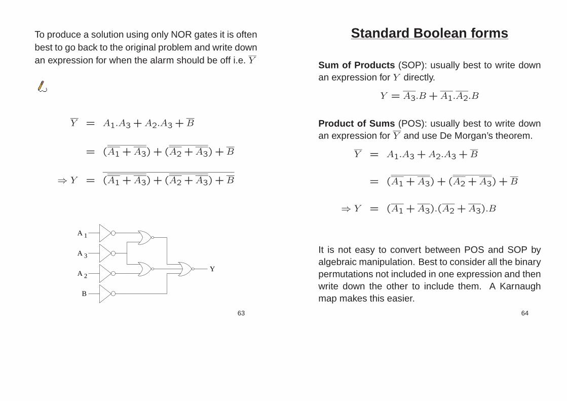
To produce a solution using only NOR gates it is oftenbest to go back to the original problem and write downan expression for when the alarm should be off i.e. Y
Y = A1.A3 + A2.A3 + B
= (A1 + A3) + (A2 + A3) + B
⇒ Y = (A1 + A3) + (A2 + A3) + B
A 1
A 3
A 2Y
B
63
Standard Boolean forms
Sum of Products (SOP): usually best to write downan expression for Y directly.
Y = A3.B + A1.A2.B
Product of Sums (POS): usually best to write downan expression for Y and use De Morgan’s theorem.
Y = A1.A3 + A2.A3 + B
= (A1 + A3) + (A2 + A3) + B
⇒ Y = (A1 + A3).(A2 + A3).B
It is not easy to convert between POS and SOP byalgebraic manipulation. Best to consider all the binarypermutations not included in one expression and thenwrite down the other to include them. A Karnaughmap makes this easier.
64

VHDL
Computer-aided design tools are required for the de-velopment of complex digital systems. These toolsenable the simulation, modelling and testing of de-signs before they are built.
A hardware description language is required to de-scribe the systems. It must be clear and readable forthe designer, yet sufficiently precise to enable rigor-ous testing of the design.
Very high speed integrated circuit hardware descrip-tion language,
abbreviated VHDL, has been developed over manyyears and is the IEEE standard 1076-1993.
65
Structure of VHDL
VHDL describes circuits in terms of design entities.Each entity consists of two parts. The interface andthe architecture specification.
entity compont name is
list of input and output portsend compont name;
architecture arch name of compont name is
declarations of internal signals;begin
description of what the the entity doesand how it is implemented
end arch name;
66

Definition of Logic Gates
entity INV isport(A : in BIT;
Y : out BIT);end INV;
architecture IMOD of INV isbeginY <= not A;
end IMOD;
entity NAND2 isport(A, B : in BIT;
Y : out BIT);end NAND2;
architecture NA2M of NAND2 isbeginY <= not (A and B);
end NA2M;
67
Definition of More Logic Gates
entity NOR2 isport(A, B : in BIT;
Y : out BIT);end NOR2;
architecture NO2M of NOR2 isbeginY <= not (A or B);
end NO2M;
entity NOR3 isport(A, B, C : in BIT;
Y : out BIT);end NOR3;
architecture NO3M of NOR3 isbeginY <= not (A or B or C);
end NO3M;
68

Using a Gate in a Larger Design
To use a gate directly in a larger design you can usethe following syntax.
unique label to refer to this version of the gate:
entity
name of gate entity(
name of gate architecture)
port map
(
‘port list’ of signals connected to gate);
eg.
V1:entity INV(IMOD) port map(A, ABAR);
69
Plant Alarm Using NAND Gates
entity PLANT ALARM is
port(A1, A2, A3, B : in BIT;
Y : out BIT);
end PLANT ALARM;
architecture NAND GATES of PLANT ALARM is
signal A1X,A2X,A3X,R12,R3 : BIT;
begin
I1:entity INV(IMOD) port map(A1,A1X);
I2:entity INV(IMOD) port map(A2,A2X);
I3:entity INV(IMOD) port map(A3,A3X);
N1:entity NAND3(NA3M)
port map(A1X,A2X,B,R12);
N2:entity NAND2(NA2M)
port map(A3X,B,R3);
N3:entity NAND2(NA2M)
port map(R12,R3,Y);
end NAND GATES;
70

Plant Alarm Using NOR Gates
entity PLANT ALARM is
port(A1, A2, A3, B : in BIT;
Y : out BIT);
end PLANT ALARM;
architecture NOR GATES of PLANT ALARM is
signal A1X,A2X,A3X,BX,R1,R2 : BIT;
begin
I1:entity INV(IMOD) port map(A1,A1X);
I2:entity INV(IMOD) port map(A2,A2X);
I3:entity INV(IMOD) port map(A3,A3X);
I4:entity INV(IMOD) port map(B,BX);
N1:entity NOR2(NO2M)
port map(A1X,A3X,R1);
N2:entity NOR2(NO2M)
port map(A2X,A3X,R2);
N3:entity NOR3(NO3M)
port map(R1,R2,BX,Y);
end NOR GATES;
71
Handout 1 Section D
Karnaugh Maps for Logic Design
In this section we introduce Karnaugh maps and showhow they can be used to design combinatorial logiccircuits.
Static and dynamic hazards are introduced and tech-niques for removing them using Karnaugh maps aredescribed.
Finally, there is a discussion of the relationship be-tween Karnaugh maps and unit-distance codes.
72

Karnaugh Map
Karnaugh maps are a powerful visual tool for carry-ing out simplification and manipulation of logic expres-sions with up to 5 input variables.
The Karnaugh map is a rectangular array of cells. Eachpossible state of the input variables corresponds uniquelyto one of the cells, and in the cell we write the corre-sponding output state.
Y = A3.B + A1.A2.B
3A
2A
A1
1 111
1B
11
10
00 01 11 10
00
01
A1
3A
A2
1 111
1
B
73
Map B on the Karnaugh map.
1
1
1
1
1
1
1
1
C
B
D
A
01
1
1
1
1
1
1
00 01 11 10
00
11
10
ABCD
1
1
Map D on the Karnaugh map.
11
11
1
1
1
1
C
B
D
A
01
11
11
1
1
00 01 11 10
00
11
10
ABCD
1
1
74

Map A.B on the Karnaugh map.
1
1
1
1
C
B
D
A10
1
1
1
1
00 01 11
00
01
11
10
ABCD
Map B.D on the Karnaugh map.
1 1
1 1C
B
D
A10
1
1
1
1
00 01 11
00
01
11
10
ABCD
75
Map the following expression on a Karnaugh map.
A.B.C.D + A.C.D + A.C
1
1 1
1
1
1
1C
B
D
A
00
01
1
1
1 1
1
00 01 11 10
11
10
ABCD
1
1
76

For a 4 variable Karnaugh map here are the shapesthat different Boolean terms produce:
1
1 1
1 1
1 11 1 1 1
1 1 1 1
1111
Four variable expressioneg. A.B.C.D
Three variable expressioneg. A.B.C
Two variable expressioneg. A.B
One variable expressioneg. A
or
Plus rotations of these shapes by 90 degrees.
Remember that the Karnaugh map wraps round top-bottom and side-to-side.
77
Simplify A.B.D +B.C.D +A.B.C.D+C.D using aKarnaugh map.
1
1
1
1
1
1 1
A
C
B
A.B
D
C.D
1
1
CD 00 01 11 10
00
01
11
10
AB
1 1
1
1 1
A.B
C.D
Thus the simplified expression is:
A.B + C.D
78

Karnaugh Map Circuit Design
For a circuit using NAND gates:
• Write down simplest sum-of-products expressionfor the output from the Karnaugh map.
• Use De Morgan to convert this to an expressionusing NAND gates.
For a circuit using NOR gates:
• Use the Karnaugh map to write down simplestsum-of-products expression for the inverse of theoutput . This involves finding terms to cover theblanks between the boxes filled with 1s.
• Use De Morgan to convert this to an expressionusing NOR gates.
79
1 111
1B
3A
1A
2A
NAND gates for the power-station fans example:
Y = A3.B + A1.A2.B
= (A3.B).(A1.A2.B)
NOR gates for the power-station fans example:
2A
11 A
A
A 1
A 2
A
A
3A 3
2
3 A
1 1B
11
1
1 1B
11
1
1 1B
11
1
Y = A1.A3 + A2.A3 + B
= (A1 + A3) + (A2 + A3) + B
⇒ Y = (A1 + A3) + (A2 + A3) + B
80

A 1
A 2
A 3
B Y
A 2
A 3
A 1
B
Y
81
Mapping the Inverse
So far the rule has been ‘map the 1s to produce a sim-ple NAND circuit and map the 0s (or gaps) to producea simple NOR circuit.’
Sometimes you can produce a simpler circuit by map-ping the opposite way (i.e. 0s for NAND and 1s forNOR) and then use a final inverter gate to change theoutput back again.
1
1
1
1 11
1
C
B
D
AFor example, if we require aNOR solution for this map thenit is probably easiest to use
Y = A.B + C.D
= (A + B) + (C + D)
82

Other Sizes of Karnaugh Map
A three variable Karnaugh map.
C
A
B
00 01 11 10AB
C
1
0
83
Other Sizes of Karnaugh Map
A five variable Karnaugh map.
A
E
D
B
C
10
AB
E=0
1011010000 01 11 10
00
01
11
E=1
CD
84

Don’t Care States
In some applications the output state for certain com-binations of input variables may not matter. Such statesare known as don’t care states and are marked withan X on the Karnaugh map.
They can be chosen to be 0 or 1, whichever helps toproduce the simplest logic (i.e. fewest, simplest terms).
For example suppose, in the power-station fans ex-ample, it happens to be impossible for fan number 2to fail on it’s own. We therefore don’t care whether ornot the alarm goes off when only fan number 2 fails(because we know that, in practice, this situation willnever occur). This would make A1.A2.A3.B a don’tcare state.
85
3A
1A
2A
1 111
1B
NAND gates for the power-station fans example with don’tcare state A1.A2.A3.B.
Y = A3.B + A2.B
= (A3.B).(A2.B)
2
A 3
A
1A
1 1B
11
1
NOR gates for the power-station fans example with don’tcare state A1.A2.A3.B.
Y = A2.A3 + B
= (A2 + A3) + B
⇒ Y = (A2 + A3) + B
86

A 3
A 2
B Y
A 2
A 3
B
Y
87
Hazards
A static hazard is when a signal undergoes a mo-mentary transition when it is supposed to remain un-changed.
A dynamic hazard is when a signal changes morethan once when it is supposed to change just once.
Static 1-hazard
Static 0-hazard
Dynamic hazard
Dynamic hazard
Logic 0Logic 1
Logic 0Logic 1
Time
Logic 0Logic 1
Logic 0Logic 1
88

Static 1-Hazard
T
XY
Z
U
V
W
Y
T
U
V
W
Time
Consider whathappens whenZ=1 and X=1and Y changesfrom 1 to 0.
This circuitimplementsW=X.Y+Z.Y
89
Removing Hazards
• Fix a static 1-hazard by drawing the Karnaughmap of the output concerned. Make sure all thesum-of-products terms overlap.
• Fix a static 0-hazard by drawing the Karnaughmap of the inverse of the output concerned. Makesure all the sum-of-products terms representingthe inverse overlap.
• Fix dynamic hazards by redesigning the circuit tosimplify the logic. (This is a 3rd year topic; don’tworry about dynamic hazards for now.)
90

Removing the Hazard
W = X.Y + Z.Y
Z1 11
Y
X
1
W = X.Y + Z.Y + X.Z
Y
1 11
X
Z
1
91
Hazard-Free Circuit
The hazard is removed from the circuit by adding anextra gate to compute the term added to the Karnaughmap: W = X.Y + Z.Y + X.Z
W
XY
Z
92
Unit Distance Codes: Motivation
Applications exist where a code is required in whichnot more than one bit changes between consecutivenumbers.
For example, a shaft encoder.
Note the potential for ambiguity during the transitionfrom 0111 to 1000.
93
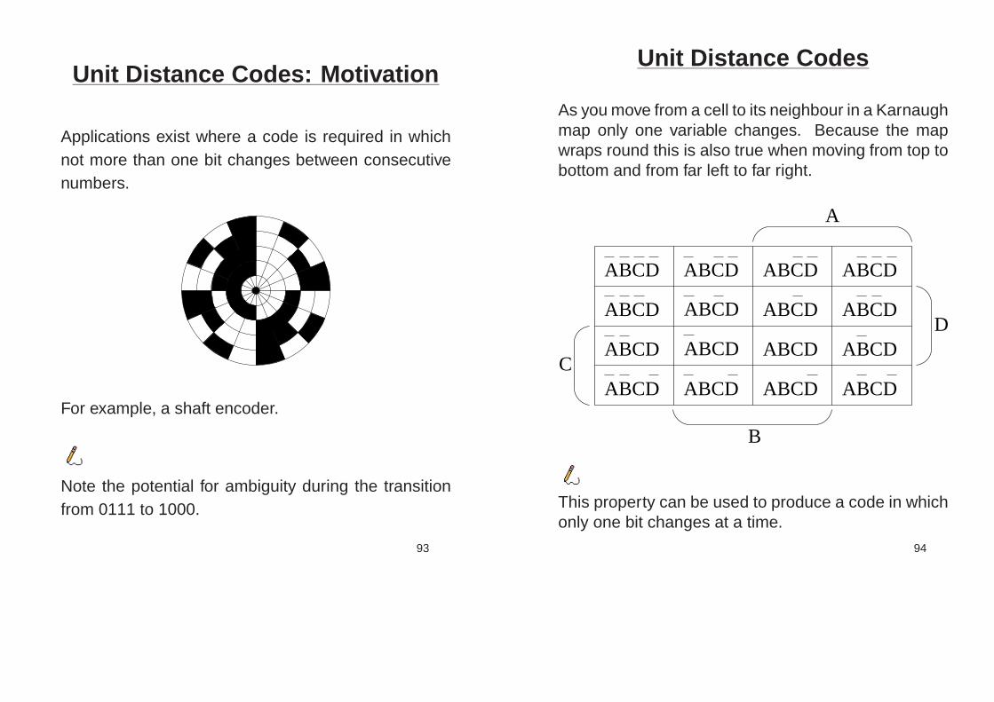
Unit Distance Codes
As you move from a cell to its neighbour in a Karnaughmap only one variable changes. Because the mapwraps round this is also true when moving from top tobottom and from far left to far right.
ABCD
ABCD
ABCD
ABCD
ABCD
ABCD
ABCD
ABCD
ABCD
ABCD
ABCD
ABCD
ABCD
ABCD
ABCD
ABCD
A
B
C
D
This property can be used to produce a code in whichonly one bit changes at a time.
94

An example of generating a unit distance code with aKarnaugh map.
C
B
D
A
A B C D A B C D0 0 0 0 1 1 0 00 0 0 1 1 1 0 10 0 1 1 1 1 1 10 0 1 0 1 1 1 00 1 1 0 1 0 1 00 1 1 1 1 0 1 10 1 0 1 1 0 0 10 1 0 0 1 0 0 0
95
• This particular unit distance code is called theGrey code.
• Other unit distance codes are possible using adifferent path around the Karnaugh map.
A unit distance code can be used to produce an im-proved shaft encoder.
96