Embed Size (px)
Citation preview

Plasma Processing
for Integrated Circuits

Plasma processing for integrated circuits
Outline
• Introduction to semiconductor processing
–chips-
• Definition of a glow discharge
–plasma-
• Plasma Etch Chemistry
-the magic in the process-
• Atomic Layer Etch
-(neutral beam plasma etching)-
2

First IC, 1958 at TI
•>2.9 billion transistors/die
Intel’s 22nm chip
Moore’s Law
3

How small is small
50nm ~1000X smaller
than human hair diameter
4

Older Generation chip
FET’s (gates)
Cu Wires
Cu Wires-damascene Cu Vias Tungsten damascene
Studs-
Last level
of Cu wires
M1
M2 V1
STI -damasecne
‘Logic Transistor’
5

Newer Generation chips
6

The loop of Wafer fabrication
Etching
7

Inside a 300mm wafer fab
http://www.youtube.com/watch?v=yaASEMAMCNM
8

• The Silicon Cylinder is Known as an Ingot
• Typical Ingot is About 1 or 2 Meters in Length
• Can be Sliced into Hundreds of Smaller
Circular Pieces Called Wafers
STARTING from the Beginning…….
9

Microfabrication deposit-pattern-etch-repeat
(a)
(b)
(c)
(d)
(e)
(f)
(g)
(h)
10

Building a
‘chip’ by
depositing,
pattern and
etching
layers
11

Selective layer removal
and anisotropy are
keys to
microfabrication
12

Two Kinds of Etching or Removal methods
13

Plasma processing for DRY etching of
integrated circuits Outline
• Introduction to semiconductor processing
–chips-
• Definition of a glow discharge
–plasma-
• Plasma Etch Chemistry
-the magic in the process-
• Atomic Layer Etch (neutral beam plasma etching)
Plasma processing?
Plasmas can deliver a high, diverse but selective, reactivity to a surface
without heat, and can therefore access a parameter space in materials
processing, which is not easily accessible with strictly chemical methods
14

What is a Plasma?
ionized gas consisting of
atoms, electrons, ions, molecules,
molecular fragments, and
electronically excited species
(informal definition)
15

Plasma – The fourth state of matter
http://www.plasmatreat.com/plasma-
technology/what-is-plasma.html
16

ENERGY
The reactive species are created in the plasma independently of substrate
The reactivity of the plasma can be tuned by carefully choosing the plasma
operating conditions (gases, flows, power, pressure, etc.)
Plasma contains ‘Electrical’ Particles (ions, electrons,.. ) and highly reactive gas
species… Through ion bombardment, additional energy can be provided to a
surface
It emits light glow (O2-pale yellow, N2-pink, CF4-blue, SF6-white blue, Ar-red, …)
17

Densities of plasma species in an O2 plasma
18

19

Ultrahigh Vacuum High Vacuum Rough Vacuum
Typical Low Pressure
Plasma Processing
Vacuum (units)
1 atm. 1.3x10⁻³ 1.3x10⁻⁶ 1.3x10⁻⁹
760 Torr 1 Torr 1 mTorr 1x10⁻⁶ Torr
1 Torr =
1 mm-Hg
101,333 Pa 133 Pa 0.133 Pa 0.133x10⁻³ Pa
1 Pascal =
1 N/m2
20

Collisions and Mean Free Path
Gas Density
n = P/ kT
l ~1/sn
Cross-section
s ~ pd2
d
Rigorous Hard Sphere Collisions: l = kT / 2 pd2P
lAr(cm) ~ 8 / P (mTorr) 15 22.6 10 cms
Ar
21
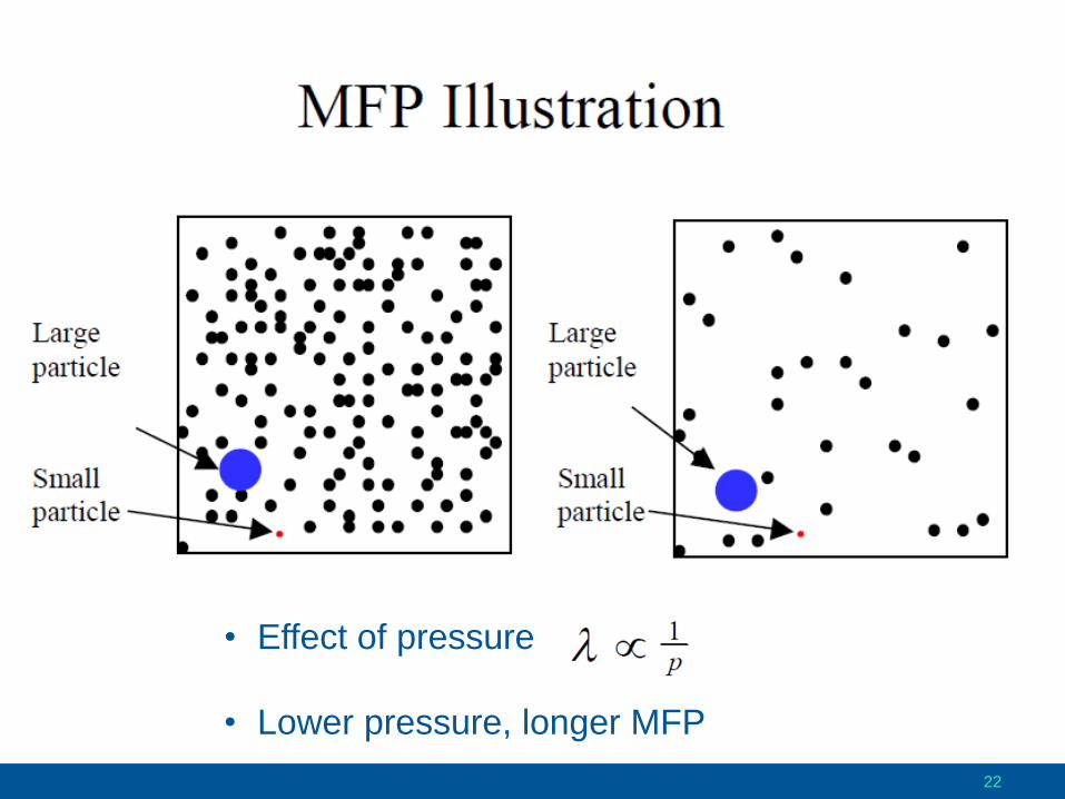
• Effect of pressure
• Lower pressure, longer MFP
22

23

How is a Plasma produced?
• Gas breakdown by Avalanche Ionization
e-
e-
e-
e- A+
A+
A+
A+
A+
e-
e-
A
+
-
Anode
Cathode
24

25

Basic Plasma Etch Tool
Vacuum pump
Environmental concerns
Abatement/Scrubbing Input gasses
Chemistry
Etching process
Chemical, Physical or combined
Wafer
e
Vacuum pump
Environmental concerns
Abatement/Scrubbing Input gasses
Chemistry
Etching process
Chemical, Physical or combined
e e
e
e
e
26

Various Plasma chamber configuration types
27

What do we need to know about
plasma?
substrate
radicals,
molecular fragments
ions Wall Wall
gas
(ng)
Gas flow
pumping pumping
electrons
ne, Te
Power
excited atoms
and molecules
light
reaction
products secondary
electrons
PLASMA
28

neni
r 0
Electron and Ion Loss to the Substrate and Walls
- the plasma sheath -
electrons are much more mobile than ions
me = q<t>/me >> q<ti>/mi = mi
neni
r 0
neni
-
-
- - - -
-
- - - -
chamber
29

30

Electron Collisions
• Elastic Collisions: – Ar + e Ar + e
– Gas heating: energy is coupled from e to the gas
• Excitation Collisions - Ar + ehot Ar* + ecold, Ar* Ar + hn - Responsible for the characteristic plasma “glow” - Eelectron>Eexc (~11.55 eV for argon)
• Dissociation: - O2 + ehot 2O + ecold or O2 + ehot O + O+ + 2ecold - Creates reactive chemical species within the plasma - Eelectron > Ediss (5.12 eV for oxygen)
• Ionization Collisions: - Ar + ehot Ar+ + 2ecold - electrical energy into producing more e_
- Eelectron > Eiz (15.76 eV for argon)
31

Surface modification (oxidation,
nitridation, etc…)
Dry Etching Spectrum
32

T. Tagaki, J. Vac. Sci. Technol. A 2, 382 (1984)
Flux of 1015 ~1 monolayer per second
33

1. ‘Sputtering’ Etching
2. ‘Chemical’ Etching
3. Energetic Ion Enhanced Etching
4. Protective Ion Enhanced Etching
Basic Methods of Plasma Etching
34

1. Physical (Sputtering)
35

2
36

3 Physical + Chemical:
The ions enhance the chemical etching
mechanisms and allow anisotropic etching
37

for etching Silicon
38

4
39

40

Example of protective etching
41

Anisotropic etch mechanisms
42

Chemistry used to optimize etch Si SiO2 + CF4 + [ H2 or O2] many different etch results Chemistry!!
43

Plasma processing for integrated circuits
Outline
• Introduction to semiconductor processing
–chips-
• Definition of a glow discharge
–plasma-
• Plasma Etch Chemistry
-the magic in the process-
• Atomic Layer Etch (neutral beam plasma etching)
44

The Desired Dry Etching Process
• Reactant + Material volatile products
*Can add reactivity and/or isotropy still need volatile products!
material material
material material
+
Requires Chemistry Understanding!! + ?
45

46

• Halogens form strong bonds with ‘electropositive’ elements
• Halides are relatively volatile
47

Fluorine • Widely used in plasma etch of
semiconductors (due to its high
reactivity)
• One of the most reactive
elements
• Si + CF4 SiF4
• W + CF4 WF6
• Wide variety of source gases
• CF4
• CHF3
• CH2F2
• CH3F
• SF6
48

Fluorine Plasma application
• Shallow (and deep) trench isolation (Si etch) – SF6 plasma
– Allows PMOS and NMOS on same chip
• Gate sidewall (Poly-Si) – CH3F, CF4
– Sidewall is the difference between fast and smoking fast
• Interconnects (SiO2, SiN) – CF4, CHF3, C4F8
– Allows path to forms the ‘insulation’ around the wires…
• TSV and Protective over coat – Access to the outside world
Source: Samsung
49
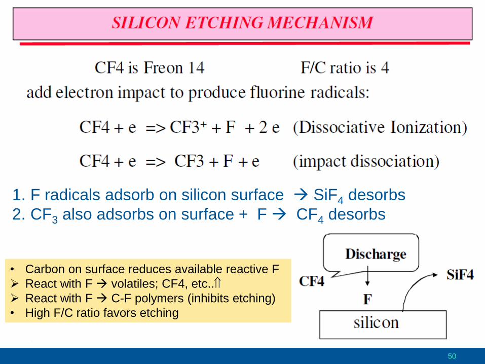
1. F radicals adsorb on silicon surface SiF4 desorbs
2. CF3 also adsorbs on surface + F CF4 desorbs
• Carbon on surface reduces available reactive F
React with F volatiles; CF4, etc..
React with F C-F polymers (inhibits etching)
• High F/C ratio favors etching
50

51

Typical etch optimization experiment
NON-optimized etch
1. Choose gasses
2. Etch test at different power/bias/pressure
3. SEM cross section Optimized etch
Over-etch
Undercut
52

Influencing reactions through Chemistry
• Addition of various gasses can influence the reactions and rates
• CF4 + e CF3 + F + e +Si SiF(4) Lowers etch Si etch rate
+ H HF ; C/F ratio
• C + O CO or CF3 + O COF2 + F C/F ratio
+ F CF(4)
53

Adjust C:F ratio
through
F-carrier
molecule
54

55

Selectivity mechanism for Si vs SiO2 (and SiN)
M. Schaepkens, et al., JVST A, 1999
Schematic view of fluxes incident on and
outgoing from the surface of
(a) Si
Si film, no volatile product between Si and
carbon exists
thick steady-state fluorocarbon film can
develop.
SiO2 film, most carbon is consumed in
reactions with oxygen from SiO2film
thin steady-state fluorocarbon film forms
allowing more efficient Si-removal by F
(The Si3N4 film has a moderate
ability to react with carbon,
steady-state fluorocarbon film of
intermediate thickness results)
(b) Si3N4 and (c) SiO2 substrates.
56

Chlorine
• Very reactive element
• Si + Cl2 SiCl4
• Al + Cl2 2AlCl3
• Highly selective gas
– Cl does not react with SiO2
• Sources for gas
– Cl2
– HCl
• Application
– Si and Metals
57

Typical Al etch plasma chemistry:
Cl2 Reduces pure Aluminum
BCL3 etches native Al2O3 (or HfO2)
N2 Dilutant and carrier gas
CHCl3 (Chloroform) Helps Anisotropy, reduce photo-resist damage
58

Bromine
• Br advantage precision (less reactive / not as spontaneous = slower more selective etch..) – HBr + Si SiBr4 + H
– HBr + Ti TiBr4 + H
– Good selectivity to oxides (SiO2, HfO2, etc..)
– Br is ‘filet-knife’ (vs. ‘F-based Axe’)
• Major source is HBr – Reddish brown liquid
• Handling of HBr – Special delivery due to low vapor
pressure
– HBr particles
• Application – Metal gate, Si levels
59

Put it all together
• We would not have Todays
‘smart’ devices without
plasma based etch
60

Plasma processing for integrated circuits
Outline
• Introduction to semiconductor processing
–chips-
• Definition of a glow discharge
–plasma-
• Plasma Etch Chemistry
-the magic in the process-
• Atomic Layer Etch (neutral beam plasma etching)
61