Embed Size (px)
Citation preview

1
Part IA Computer
Science Tripos
Hardware Practical
Classes
Year: 2016 – 2017
Dr. I. J. Wassell,
Mr. N. Batterham.

2

3
Introduction The Hardware Practical Classes accompany the Digital Electronics series of lectures. The
aim of the Practical Classes is to enable students to get hands-on experience of designing,
building, and testing and debugging of digital electronic circuits. The Digital Electronics
lecture series occupies 12 lectures in the first 4 weeks of the Michaelmas Term, while the
Practical Classes occupy the latter 6 weeks of the Michealmas Term and all 8 weeks of the
Lent Term. The Practical Classes take the form of 6 workshops where 3 are conducted in
each term. Each Workshop has an accompanying worksheet that is included in this
document, specifically:
Workshop 1 – Electronic Die;
Workshop 2 – Shaft Position Encoder;
Workshop 3 – Debouncing a Switch;
Workshop 4 – Framestore for an LED Array;
Workshop 5 – nMOS, pMOS and CMOS Inverters;
Workshop 6 – Digital-to-Analogue Converters.
In general, the workshops require some preparatory work to be done prior to the actual
workshop. Typically this involves preparing a design that you will then build, test and modify
during the practical class. Note that insufficient preparation prior to the practical classes may
compromise effective use of your time in the laboratory.
In the Practical Classes you will usually work in groups of 2, and each group is scheduled to
attend a laboratory session every other week while the Practical Classes are running. The
Practical Classes are timetabled to run every Thursday while in operation, with morning
sessions running from 10.30 until 1.00 and afternoon sessions running from 1.30 until 4.00.
Demonstrators are available during the sessions to assist you with any queries or problems
you may have. Here are some additional points to bear in mind regarding the Practical
Classes:
You will be allocated a laboratory session every other week. Please make sure you
stick to your timetabled session, otherwise the numbers per session become
unbalanced giving rise to problems in terms of equipment availability and
demonstrator support;
Arrive promptly and begin your work in a timely manner. This will maximise the
probability of completing a workshop before the end of the laboratory session. This is
particularly important for those in the morning sessions, since there is only a short
interval before the afternoon session begins;
Make sure you keep up with the workshop schedule and get each workshop ‘ticked’;
During week 3 of the accompanying Digital Electronics lecture series, a lecture to
introduce the Hardware Practical Classes will be given. It is important that you attend
this lecture, particularly if you have no prior experience of electronics;
During subsequent lectures of the Digital Electronics course, introductory guidance
will be given prior to the first running of Workshop 2 and Workshop 3.

4
5
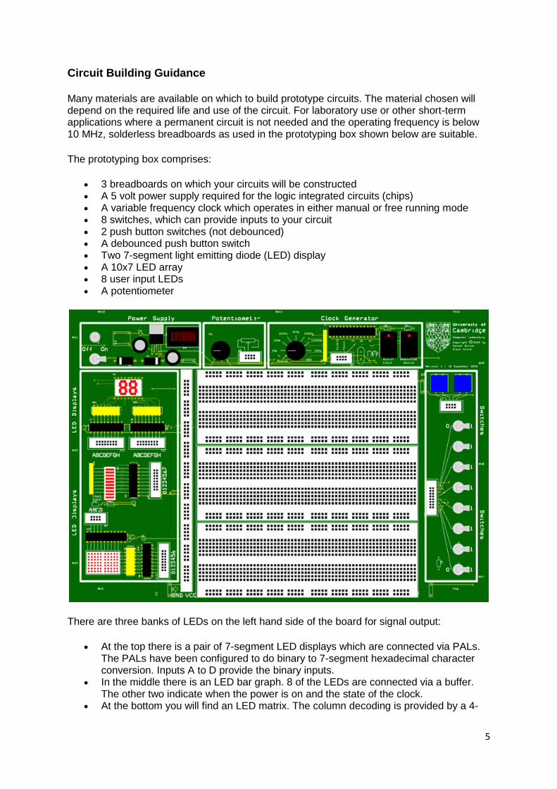
Circuit Building Guidance
Many materials are available on which to build prototype circuits. The material chosen will depend on the required life and use of the circuit. For laboratory use or other short-term applications where a permanent circuit is not needed and the operating frequency is below 10 MHz, solderless breadboards as used in the prototyping box shown below are suitable.
The prototyping box comprises:
3 breadboards on which your circuits will be constructed A 5 volt power supply required for the logic integrated circuits (chips) A variable frequency clock which operates in either manual or free running mode 8 switches, which can provide inputs to your circuit 2 push button switches (not debounced) A debounced push button switch Two 7-segment light emitting diode (LED) display A 10x7 LED array 8 user input LEDs A potentiometer
There are three banks of LEDs on the left hand side of the board for signal output:
At the top there is a pair of 7-segment LED displays which are connected via PALs. The PALs have been configured to do binary to 7-segment hexadecimal character conversion. Inputs A to D provide the binary inputs.
In the middle there is an LED bar graph. 8 of the LEDs are connected via a buffer. The other two indicate when the power is on and the state of the clock.
At the bottom you will find an LED matrix. The column decoding is provided by a 4-

6
to-16 line decoder (inputs A to D) and the row value is supplied via a buffer (inputs 0 to 6).
Using the Breadboard
A breadboard has many strips of metal which run underneath the board. The metal strips are laid out as shown in red below, horizontally along the two lines at the top and bottom, and vertically to join six holes together in the central section.
These strips connect the holes on the top of the board. This makes it easy to connect components together to build circuits. To use the breadboard, the legs of components are placed in the holes (the sockets). The holes are made so that they will hold the component in place. Each hole is connected to one of the metal strips running underneath the board.
The long top and bottom row of holes are usually used for power supply connections. The rest of the circuit is built by placing components and connecting them together with jumper wires. Chips can be placed in the middle of the board so that half the legs are on one side of the middle line and half are on the other side. A completed circuit might look like the following.
Careful planning of the circuit layout simplifies wiring, minimizes errors and makes debugging easier. Try to arrange the circuit for a logical signal flow, usually inputs on the left and outputs on the right. This helps anyone looking at the board to find easily sections of the circuit and trace signals through it. Wherever possible, all ICs should be pointed in the same direction to reduce the chance of one being put in backwards. This also makes it easier to keep track of pin numbers when wiring and debugging. Colour coded wiring is an easy way to reduce wiring errors and aid the process. If possible, build and test one section of the circuit at a time to simplify debugging before connecting the sections
7
together. Keep connecting wires as short as possible and route them around ICs so that a defective IC can be replaced without removing and often incorrectly replacing the wires. While all this may seem laborious, the time spent in careful construction and checking is well repaid by having more circuits work first time.
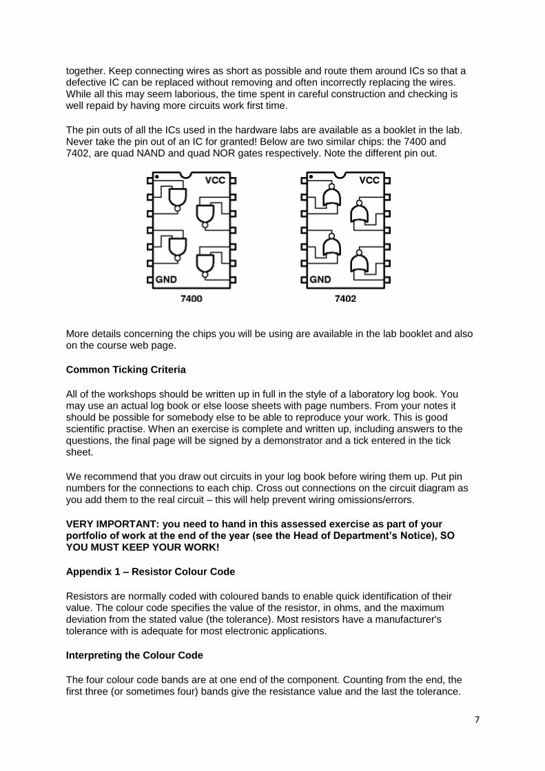
The pin outs of all the ICs used in the hardware labs are available as a booklet in the lab. Never take the pin out of an IC for granted! Below are two similar chips: the 7400 and 7402, are quad NAND and quad NOR gates respectively. Note the different pin out.
More details concerning the chips you will be using are available in the lab booklet and also on the course web page.
Common Ticking Criteria
All of the workshops should be written up in full in the style of a laboratory log book. You may use an actual log book or else loose sheets with page numbers. From your notes it should be possible for somebody else to be able to reproduce your work. This is good scientific practise. When an exercise is complete and written up, including answers to the questions, the final page will be signed by a demonstrator and a tick entered in the tick sheet.
We recommend that you draw out circuits in your log book before wiring them up. Put pin numbers for the connections to each chip. Cross out connections on the circuit diagram as you add them to the real circuit – this will help prevent wiring omissions/errors.
VERY IMPORTANT: you need to hand in this assessed exercise as part of your portfolio of work at the end of the year (see the Head of Department’s Notice), SO YOU MUST KEEP YOUR WORK!
Appendix 1 – Resistor Colour Code
Resistors are normally coded with coloured bands to enable quick identification of their value. The colour code specifies the value of the resistor, in ohms, and the maximum deviation from the stated value (the tolerance). Most resistors have a manufacturer's tolerance with is adequate for most electronic applications.
Interpreting the Colour Code
The four colour code bands are at one end of the component. Counting from the end, the first three (or sometimes four) bands give the resistance value and the last the tolerance.
8
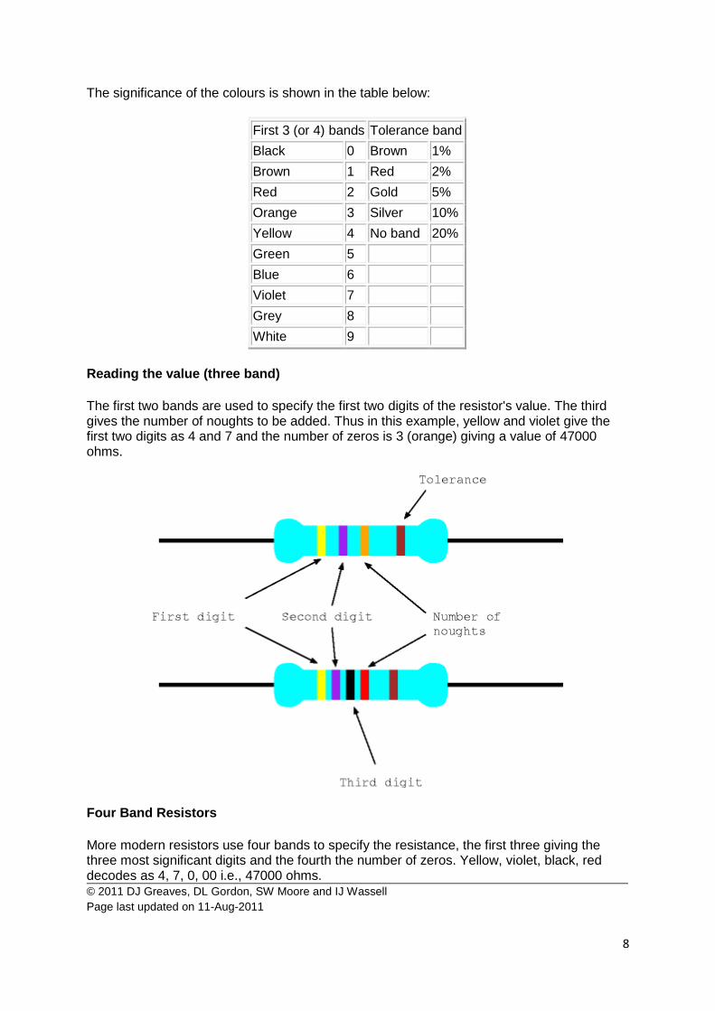
The significance of the colours is shown in the table below:
First 3 (or 4) bands Tolerance band
Black 0 Brown 1%
Brown 1 Red 2%
Red 2 Gold 5%
Orange 3 Silver 10%
Yellow 4 No band 20%
Green 5
Blue 6
Violet 7
Grey 8
White 9
Reading the value (three band)
The first two bands are used to specify the first two digits of the resistor's value. The third gives the number of noughts to be added. Thus in this example, yellow and violet give the first two digits as 4 and 7 and the number of zeros is 3 (orange) giving a value of 47000 ohms.
Four Band Resistors
More modern resistors use four bands to specify the resistance, the first three giving the three most significant digits and the fourth the number of zeros. Yellow, violet, black, red decodes as 4, 7, 0, 00 i.e., 47000 ohms.
© 2011 DJ Greaves, DL Gordon, SW Moore and IJ Wassell
Page last updated on 11-Aug-2011
9
Workshop One – Electronic Die Introduction The purpose of this lab is to build a simple electronic die using light emitting diodes (LEDs) as the display device. Digital logic chips will be used to implement the required functionality. You will construct the die on a prototyping breadboard that is housed in the 1A workshop prototyping box. Before you start wiring up the circuits, make sure you understand how the holes in the breadboard are connected and also how the pins are numbered on the logic chips – see the description in Appendix A.
Equipment and Components 1A Workshop Prototyping Box Connecting wire Red LEDs (7)
220 resistors (7)
10k resistor 74HC00 – Quad 2 input NAND gates (2) 74HC193 – Synchronous 4 bit up/down counter (1)
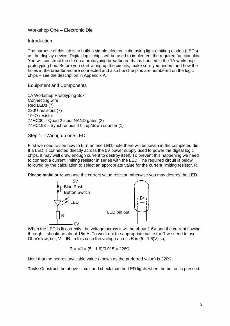
Step 1 – Wiring up one LED First we need to see how to turn on one LED; note there will be seven in the completed die. If a LED is connected directly across the 5V power supply used to power the digital logic chips, it may well draw enough current to destroy itself. To prevent this happening we need to connect a current limiting resistor in series with the LED. The required circuit is below, followed by the calculation to select an appropriate value for the current limiting resistor, R. Please make sure you use the correct value resistor, otherwise you may destroy the LED. When the LED is lit correctly, the voltage across it will be about 1.6V and the current flowing through it should be about 15mA. To work out the appropriate value for R we need to use Ohm’s law, i.e., V = IR. In this case the voltage across R is (5 - 1.6)V, so,
R = V/I = (5 - 1.6)/0.015 = 226.
Note that the nearest available value (known as the preferred value) is 220. Task: Construct the above circuit and check that the LED lights when the button is pressed.
Blue Push-
Button Switch
R
0V
5V
LED
LED pin out
10
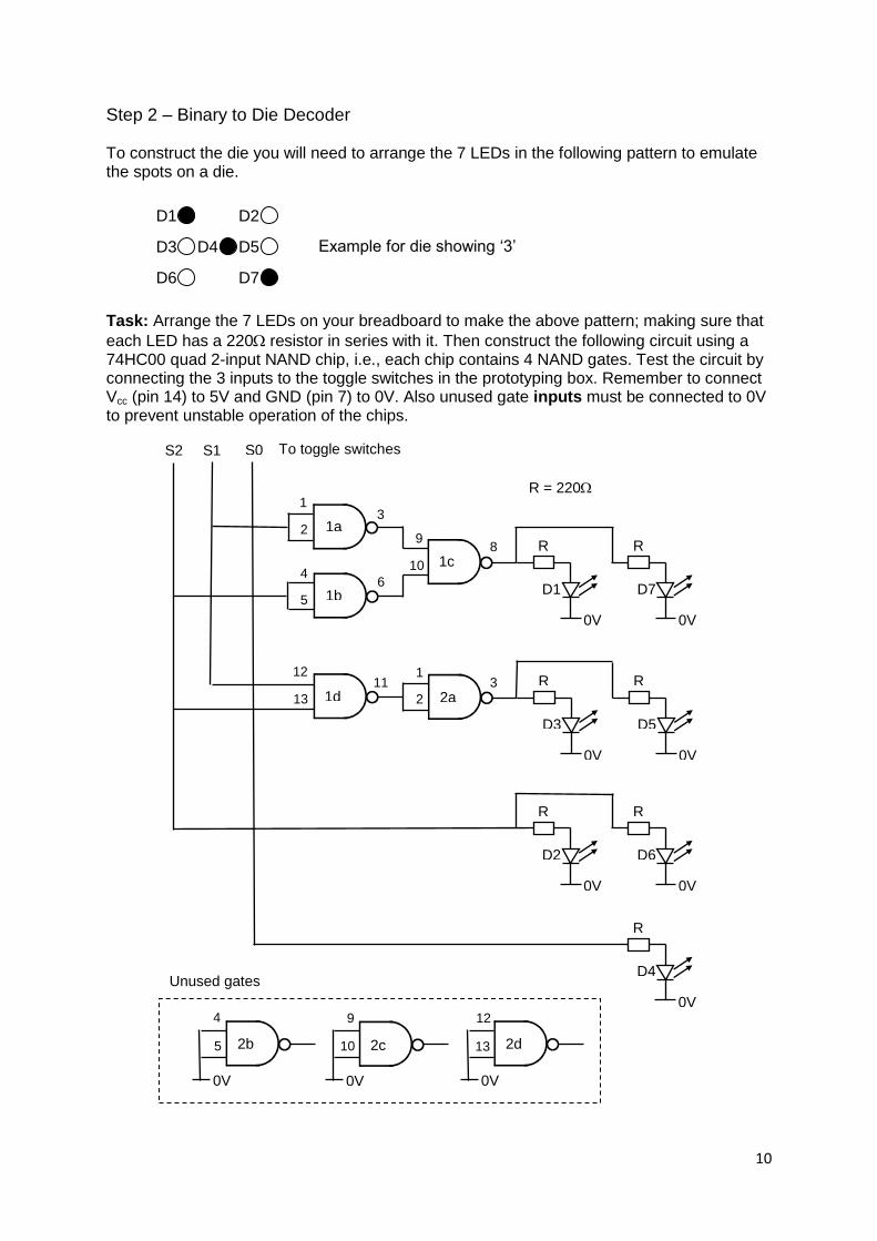
Step 2 – Binary to Die Decoder To construct the die you will need to arrange the 7 LEDs in the following pattern to emulate the spots on a die. Example for die showing ‘3’ Task: Arrange the 7 LEDs on your breadboard to make the above pattern; making sure that
each LED has a 220resistor in series with it. Then construct the following circuit using a 74HC00 quad 2-input NAND chip, i.e., each chip contains 4 NAND gates. Test the circuit by connecting the 3 inputs to the toggle switches in the prototyping box. Remember to connect Vcc (pin 14) to 5V and GND (pin 7) to 0V. Also unused gate inputs must be connected to 0V to prevent unstable operation of the chips.
D1
D3
D6
D2
D5
D7
D4
R
0V
D1
R
0V
D7
R
0V
D3
R
0V
D5
R
0V
D2
R
0V
D6
R
0V
D4
S0 S1 S2 To toggle switches
0V 0V 0V
1d 2a
2b 2c 2d
Unused gates
R = 220 1
1a
1b
1c
2 3
4
5
6
9
10
8
12
13
11 1
2
3
4
5
9
10
12
13
11
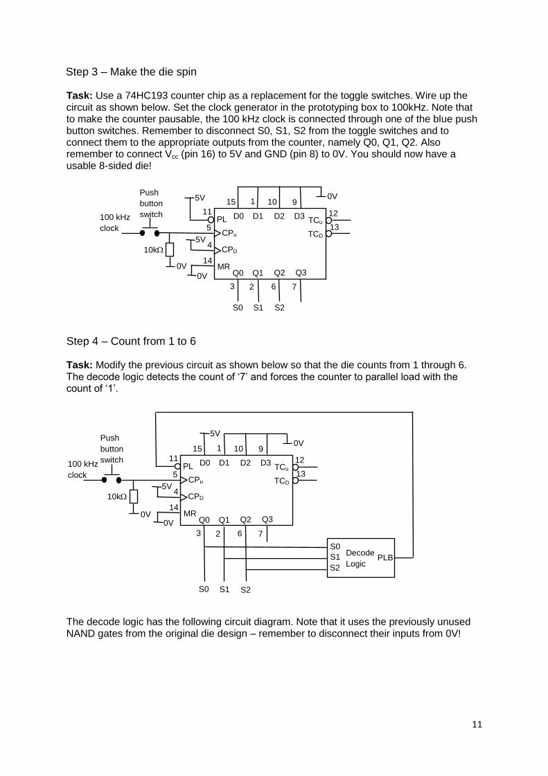
Step 3 – Make the die spin
Task: Use a 74HC193 counter chip as a replacement for the toggle switches. Wire up the circuit as shown below. Set the clock generator in the prototyping box to 100kHz. Note that to make the counter pausable, the 100 kHz clock is connected through one of the blue push button switches. Remember to disconnect S0, S1, S2 from the toggle switches and to connect them to the appropriate outputs from the counter, namely Q0, Q1, Q2. Also remember to connect Vcc (pin 16) to 5V and GND (pin 8) to 0V. You should now have a usable 8-sided die!
Step 4 – Count from 1 to 6 Task: Modify the previous circuit as shown below so that the die counts from 1 through 6. The decode logic detects the count of ‘7’ and forces the counter to parallel load with the count of ‘1’. The decode logic has the following circuit diagram. Note that it uses the previously unused NAND gates from the original die design – remember to disconnect their inputs from 0V!
11 PL
5V
5 CPu
CPD
5V 4
MR 0V
14
D0
Q0
D1
15 1
D2
10 9
D3
Q1 Q2 Q3
3 2 6 7
TCu 12
13 TCD
Push
button
switch 100 kHz
clock
0V
S0 S1 S2
0V
10k
11 PL
5 CPu
CPD
5V 4
MR 0V
14
D0
Q0
D1
15 1
D2
10 9
D3
Q1 Q2 Q3
3 2 6 7
TCu 12
13 TCD
Push
button
switch 100 kHz
clock
0V
S0 S1 S2
5V
S0
S1
S2
Decode
Logic PLB
10k
0V

12
Assessment Ticking criteria: Demonstrate that your 8-sided die works and answer the following questions. Once your work has met the Common Ticking Criteria (see Introduction), get your work ticked by an assessor. Remember that you need to hand-in this assessment exercise as part of your portfolio of work (see Head of Department’s notice). In future workshops, it will be often be convenient to monitor the logical value of a signal using LEDs. Rather than wiring up discrete LEDs with serial resistors as we have done in this workshop, it will be more convenient to use the bank of 8 pre-wired LEDs which is available on the left hand side of the prototyping box. Questions 1. What die patterns are displayed for binary inputs 000 and 111? 2. How much current can each NAND gate on the 74HC00 drive? 3. How would you arrange an LED (and resistor) so that it turns on when the output of a NAND gate is low? 4. How could this reduce the number of gates you have used? I. J. Wassell 10-6-15
2d
4
2b 5 6
2c
9
10
8
12
2 13
11
S0
S1
S2
PLB
13
Workshop Two – Shaft Position Encoder
Introduction
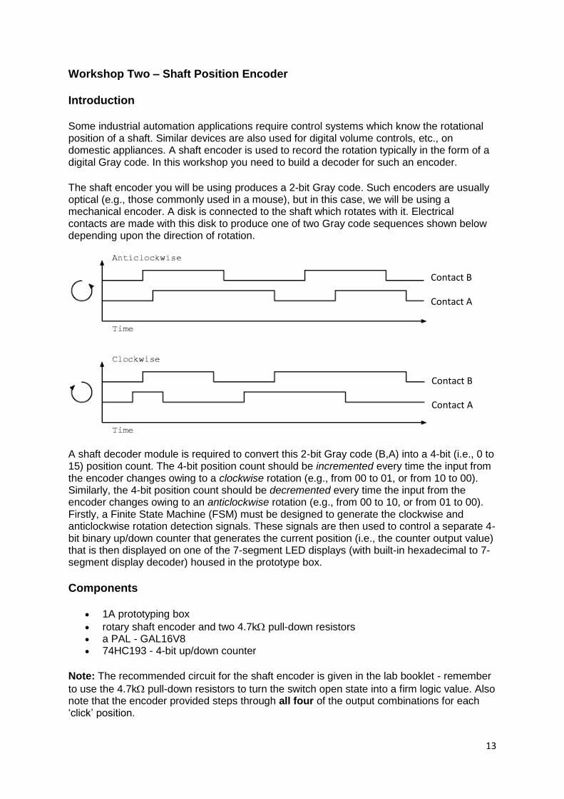
Some industrial automation applications require control systems which know the rotational position of a shaft. Similar devices are also used for digital volume controls, etc., on domestic appliances. A shaft encoder is used to record the rotation typically in the form of a digital Gray code. In this workshop you need to build a decoder for such an encoder.
The shaft encoder you will be using produces a 2-bit Gray code. Such encoders are usually optical (e.g., those commonly used in a mouse), but in this case, we will be using a mechanical encoder. A disk is connected to the shaft which rotates with it. Electrical contacts are made with this disk to produce one of two Gray code sequences shown below depending upon the direction of rotation.
A shaft decoder module is required to convert this 2-bit Gray code (B,A) into a 4-bit (i.e., 0 to 15) position count. The 4-bit position count should be incremented every time the input from the encoder changes owing to a clockwise rotation (e.g., from 00 to 01, or from 10 to 00). Similarly, the 4-bit position count should be decremented every time the input from the encoder changes owing to an anticlockwise rotation (e.g., from 00 to 10, or from 01 to 00). Firstly, a Finite State Machine (FSM) must be designed to generate the clockwise and anticlockwise rotation detection signals. These signals are then used to control a separate 4-bit binary up/down counter that generates the current position (i.e., the counter output value) that is then displayed on one of the 7-segment LED displays (with built-in hexadecimal to 7-segment display decoder) housed in the prototype box.
Components
1A prototyping box
rotary shaft encoder and two 4.7k pull-down resistors a PAL - GAL16V8 74HC193 - 4-bit up/down counter
Note: The recommended circuit for the shaft encoder is given in the lab booklet - remember
to use the 4.7k pull-down resistors to turn the switch open state into a firm logic value. Also note that the encoder provided steps through all four of the output combinations for each ‘click’ position.
Contact B
Contact A
Contact B
Contact A

14
Step 1 - shaft decoder to generate clockwise/anticlockwise signals
Design task 1: Draw a state diagram to decode this movement. Generate two independent outputs, one that goes high for one clock cycle when the shaft rotates one output combination change clockwise, namely CW, and the other for one output combination change anticlockwise, namely AW. Assume 4 states, i.e., 00, 01, 11 and 10, and make the next state equal to the current input values B and A. For example, assume we are in state 00 and the shaft rotates one output combination anticlockwise giving current input values, B=1, A=0, the next state will be 10 and the outputs are AW=1 and CW=0. Now complete the state diagram for all 4 states and for all three possible inputs per state.
Design task 2: From the state diagram, create a state transition table. Note that this table will have columns for the Current State, the Next State (remember that is the same as the current inputs) and for the clockwise (CW) and anticlockwise (AW) outputs. Now determine expressions for the AW and CW outputs. Remember that it is possible to use don’t care conditions to simplify the expressions for AW and CW. For example, one don’t care condition for both AW and CW is for the 00 to 11 state transition that we know does not ever occur. We now wish to implement a synchronous (clocked from an independent free-running clock) FSM inside a PAL.
The PAL has 8 possible output pins labelled P19 to P12 and 8 inputs labelled P2 to P9. Connect P2 to Contact A and P3 to Contact B.
This exercise can be completed by designing a four-state FSM, where the D-type flip-flops (FFs) having outputs labelled P18 and P19 hold the states. Your equations should look something like this:
P19 = P2
P18 = P3 P15 = <Some function of P3, P2, P18 and P19>
P14 = <Some function of P3, P2, P18 and P19>
P17 = P14 (note: not strictly necessary) P16 = P15 (note: not strictly necessary)
This means that FF output P19 is a registered version of its input P2 (that is connected to A) and FF output P18 is a registered version of its input P3 (that is connected to B). So the Next State is given by the current inputs P2 and P3, and the Current State is FF outputs P19 and P18. The outputs labelled P15 and P14 are the Clockwise (CW) and Anticlockwise (AW) signals respectively and are functions of the current state (P19 and P18) and the inputs (P2 and P3).
This design is a Mealy machine, since the outputs P15 and P14 generated by its combinational logic can apparently change directly in response to the inputs P2 and P3. Thus owing to ‘contact bounce’ in the switch, the inputs P2 and P3 will experience multiple transitions giving rise to unwanted multiple transitions at the output of the combinational logic. However, because we have set the PAL in to registered mode, in effect, the outputs P15 and P14 have already been registered via a D type FF on each output and so in this case we do not have to worry. However, to be on the safe side, we have also explicitly included an additional D type FF on each output. Thus P17 (ACW) is a registered version of P14 and P16 (CW) is a registered version of P15. Thus in reality, we actually have a ‘registered’ Mealy machine.

15
Very Important Point Concerning the 74HC193 4-bit up/down Counter
Fundamentally, the CW and AW signals are used to control whether the counter increments or decrements its current count value respectively, i.e., whether it up or down counts. The up/down counter has 2 separate clock inputs, one for up counting (CPU) and one for down counting (CPD). For example to make the counter increment, then a rising edge has to be applied to CPU input (essentially a pulse signal created by changing the CPU input signal from a binary ‘1’ to a binary ‘0’ and then back again), while the CPD input is held at binary ‘1’. The reverse situation applies concerning the clock inputs to make the counter decrement its value. Consequently, when generating the P15 and P14 clockwise and anticlockwise signals, we actually require the complement of the CW and AW signals (as defined previously) to provide the CPU and CPD clock signals respectively. Consequently if we are using K-maps to determine the simplified Boolean expressions for P15 and P14, we should group the ‘0’s and any don’t care states (rather than grouping the ‘1’s and the don’t care states) in the map.
NOTE: As indicated, we make the outputs from the shaft encoder (B and A) synchronous by using 2 FFs before these signals are applied to the 2 FFs that implement the FSM. To do this, make sure that the PAL compiler is in registered mode.
Implementation task 1: Now run your equations through the PAL compiler. Read the Appendix on PALs and the PAL compiler if you are unfamiliar with them. The compiler should be running on a stand-alone PC connected to the programmer.
Implementation task 2: Now connect your PAL to a rotary encoder and your two outputs to LEDs. Connect the clock to pin 1 and make sure that the output enable (pin 11) is connected to ground. To test your design start by setting the clock to 10Hz. Make sure that each LED flashes once as the rotary encoder is moved one output combination clockwise or anticlockwise.
Step 2 - count clockwise/anticlockwise pulses
Implementation task: Use the clockwise/anticlockwise signals as up/down count signals for the 74HC193 counter. Connect the output of the counter to one of the 7-segment displays. Note that the 4-bit input to each of the 7-segment displays is labelled ABCD, where A represents the most significant bit (MSB) and D the least significant bit (LSB). Also, make sure the unused inputs of the 74HC193 and connected to either 0V or 5V as appropriate.
Assessment
Ticking criteria: Write up your design and answer the following questions. Demonstrate that your rotary position counter works. Once your work has met the Common Ticking Criteria (see Introduction), get your work ticked by an assessor. Remember that you need to hand in this assessed exercise as part of your portfolio of work (see the Head of Department's notice).
Questions
1. Why didn't we ask you to debounce the inputs from the rotary encoder? 2. How fast can the rotary encoder be rotated before your circuit fails to count correctly?
16
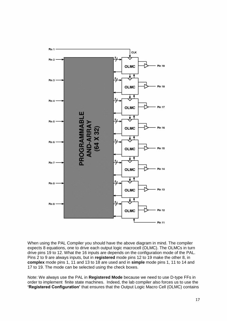
Appendix – PALs and the PAL Compiler
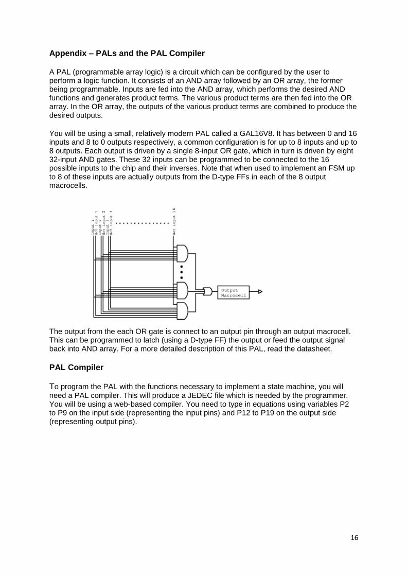
A PAL (programmable array logic) is a circuit which can be configured by the user to perform a logic function. It consists of an AND array followed by an OR array, the former being programmable. Inputs are fed into the AND array, which performs the desired AND functions and generates product terms. The various product terms are then fed into the OR array. In the OR array, the outputs of the various product terms are combined to produce the desired outputs.
You will be using a small, relatively modern PAL called a GAL16V8. It has between 0 and 16 inputs and 8 to 0 outputs respectively, a common configuration is for up to 8 inputs and up to 8 outputs. Each output is driven by a single 8-input OR gate, which in turn is driven by eight 32-input AND gates. These 32 inputs can be programmed to be connected to the 16 possible inputs to the chip and their inverses. Note that when used to implement an FSM up to 8 of these inputs are actually outputs from the D-type FFs in each of the 8 output macrocells.
The output from the each OR gate is connect to an output pin through an output macrocell. This can be programmed to latch (using a D-type FF) the output or feed the output signal back into AND array. For a more detailed description of this PAL, read the datasheet.
PAL Compiler
To program the PAL with the functions necessary to implement a state machine, you will
need a PAL compiler. This will produce a JEDEC file which is needed by the programmer. You will be using a web-based compiler. You need to type in equations using variables P2 to P9 on the input side (representing the input pins) and P12 to P19 on the output side (representing output pins).
17
When using the PAL Compiler you should have the above diagram in mind. The compiler expects 8 equations, one to drive each output logic macrocell (OLMC). The OLMCs in turn drive pins 19 to 12. What the 16 inputs are depends on the configuration mode of the PAL. Pins 2 to 9 are always inputs, but in registered mode pins 12 to 19 make the other 8, in complex mode pins 1, 11 and 13 to 18 are used and in simple mode pins 1, 11 to 14 and 17 to 19. The mode can be selected using the check boxes.
Note: We always use the PAL in Registered Mode because we need to use D-type FFs in order to implement finite state machines. Indeed, the lab compiler also forces us to use the ‘Registered Configuration’ that ensures that the Output Logic Macro Cell (OLMC) contains
18
a D-type FF. Incidentally, a ‘Combinatorial Configuration’ for the Registered Mode is also available where the OLMC does not include a D-type FF. However, we do not make use of this possibility.
The equations for each output (called P19 to P12, in that order) can consist of inputs, operators and brackets. The input must be referred to by the "P" followed by a number. Operators are &, |, ^ and ! for AND, OR, XOR and NOT respectively
Examples:
P19 = P2 A simple assignment latch
P19 = P2 ^ P3 P18 = P2 & P3
A half adder
P19 = !P19 A 1-bit counter
When you have typed in your equations, click the compile button.
© 2011 DJ Greaves, DL Gordon, SW Moore and IJ Wassell
Page last updated on 16-Jun-2016
19
Workshop Three – Debouncing a Switch
Introduction
When using a switch as an input to a digital circuit, several pit-falls may be encountered. The problem of switch `bounce' is the subject of this experiment, what it is, and ways (including an all-digital method) of overcoming it.
Components
1A prototyping box connecting wire 2 x 4K7 resistor 74HC00 - NAND gates 74HC193 counter A PAL - GAL16V8 Single pole double throw (SPDT) switch
Step 1 - Watch a switch bouncing
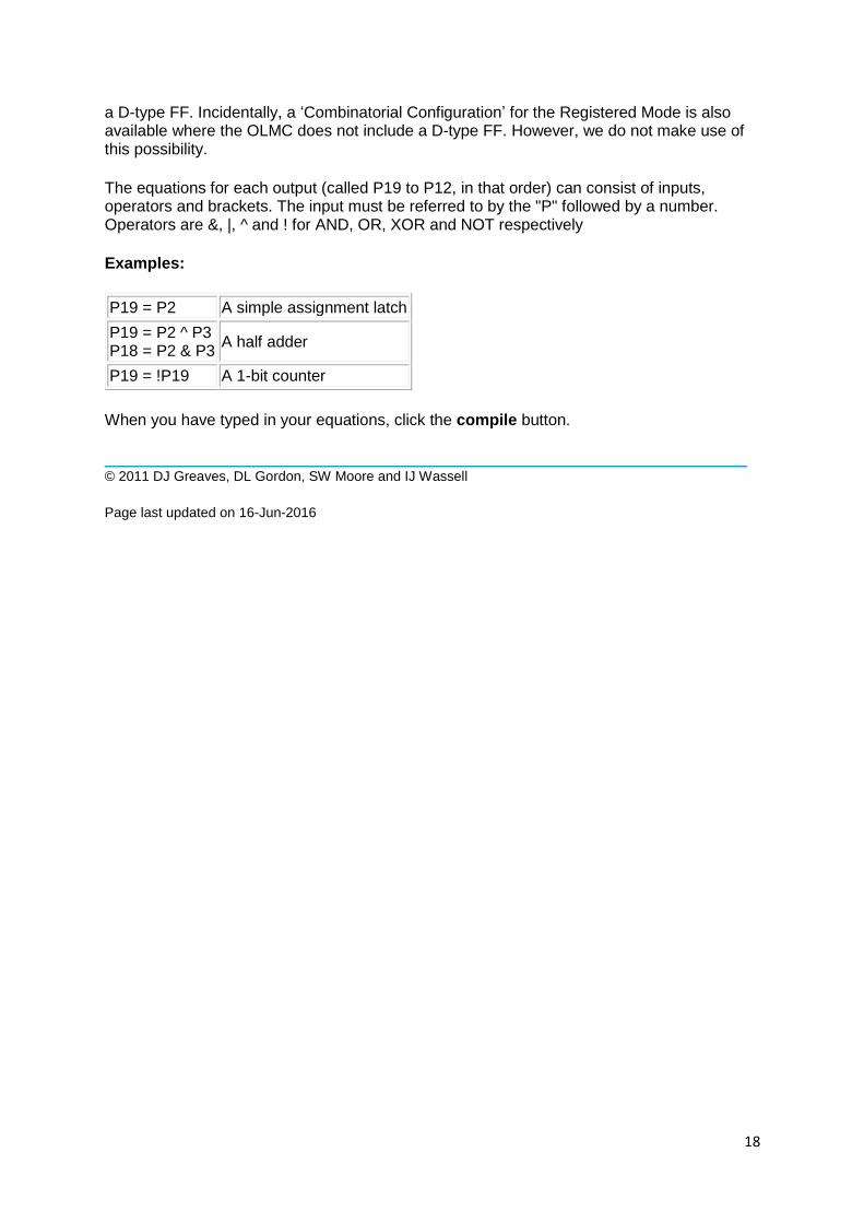
Task: Build the following circuit on a breadboard using the blue non-debounced push-switch. Connect a scope probe to the output. Look at the output on the scope as the contact is made and broken. This is best done by triggering off the switch and varying the timebase setting until the appropriate detail can be seen.
Note: The 4K7 resistor is often known as a ‘pull-up’ resistor since the Output is pulled-up to 5V when the push button switch is open.
Step 2 - Count bounces
Task: Connect the output of the circuit in Step 1 to the clock input of the counter (Note: This is the counter device used in the previous workshop, but make sure you connect the inputs appropriately so that it operates as an up-counter). Connect the counter output to the 7-segment display as was done in the previous workshop. What should happen? Why doesn't it work? The object of the next step is to debounce the switch so that counter increments just once as the switch contact is made.

20
Step 3 - Debouncing a single pole double-throw switch
You may be surprised to find that a single pole double-throw (SPDT) switch is easier to debounce than the single-throw switch employed in the previous circuit, so in the first instance we will begin by debouncing a SPDT switch. The following circuit shows a SPDT switch and two pull-up resistors. The switch you will be using is a break before make switch, i.e., it is mechanically incapable of connecting both switch terminals together. What is the relationship between the two outputs if bounces only appear on one contact at a time?
Task: Build the above circuit. Use an RS latch that takes OutputA and OutputB as inputs and produces a debounced output. Note: The switch connection arrangement used here produces a ‘High’ (i.e., 5V) output when a switch contact is open, and a ‘Low’ (i.e., 0V) output when a switch contact is closed. Thus the logical output from this arrangement is known as ‘active low’. This has the opposite sense to what is required at the inputs to the NOR gate based RS latch shown in the Digital Electronics course notes. For example from the course notes we see that a ‘High’ on the S input (and a ‘low’ on the R input) gives the ‘Set’ condition. Use bubble logic to reconfigure the NOR based RS latch to use active low inputs, i.e., where for example the ‘set’ condition is given by a ‘Low’ on the S input and a ‘High’ on the R input.
Step 4 - Debouncing the push button switch
Debouncing a switch can be done in many ways, using a variety of analogue or digital techniques. We will now implement a debouncer using a synchronous digital approach. Consequently we will use a PAL to implement a length 7 shift register (i.e., 7, D type flip-flops) with the switch output as its input. You should not use the output of the first flip-flop since it may go metastable if the input changes too near the active clock edge. When all of the other flip-flops (i.e., 6) in the shift register all become ‘Low’, the output from the debounce circuit should go ‘Low’. Similarly, when all the shift register outputs become ‘High’, the output of the debouncer should go ‘High’.
Design Hint: Consider using a 6-input OR gate to generate a signal, say LNG (active ‘Low’), to detect when the shift register outputs are all ‘Low’. In addition use a 6-input AND gate to generate a signal, say ACT (active ‘Low’) that detects when the shift register outputs are no longer all ‘High’, i.e., some switch activity has occurred. Use these 2 signals as the inputs to a 2-state Moore machine to generate the required debounced output signal. To do this, draw the required finite state machine, where the required output is the current state and the transitions between states are determined by the generated ‘input’ signals LNG and ACT. Next write down the associated state transition table and use a Karnaugh Map to generate the required next state logic for the D flip-flop. Don’t forget to

21
make use of don’t care conditions to simplify the required combinational logic.
Task: Design, build and test this digital switch debouncer.
Assessment
Ticking criteria: Write up your experimental data and final design, and then answer the following questions. Demonstrate that your debouncer works.
Once your work has met the Common Ticking Criteria (see Introduction), get your work ticked by an assessor. Remember that you need to hand in this assessed exercise as part of your portfolio of work (see the Head of Department's notice).
Questions
1. Why is a switch debouncer necessary? 2. How should you choose the clock frequency for the PAL based debouncer?
© 2011 DJ Greaves, DL Gordon, SW Moore and IJ Wassell Page last updated on 13-Jun-2016

22

23
Workshop Four - Framestore for an LED Array
Introduction
This aim of this experiment is design, build and test a framestore (a piece of equipment that stores an image) implemented using a Static Random Access Memory (SRAM), two light emitting diode (LED) arrays to display the image and some control logic.
The design uses the SRAM as a framestore for two 5x7 LED arrays. The LED display is made up from individual LEDs which are connected in a grid. Connecting a row (through a current limiting resistor) to the power rail and a column to ground lights the LED where they cross. This means that although each LED can be lit individually, an arbitrary pattern cannot be displayed merely by applying constant voltages to the row and column inputs. Instead, the array must be scanned, preferably at a rate at which the display does not appear to flicker. In this experiment, the pattern to be displayed is to be read from an SRAM.
Components
1A prototyping box connecting wires Holtek HT6116-70 SRAM 74HC541 octal tri-state buffer 74HC00 quad 2-input NAND gates 74HC193 4-bit synchronous binary counter 74HC74 dual D-type flip-flop Binary-coded decimal (BCD) hex switch

24
Step 1 - Make the LED matrix light up
Task: Use the 74HC193 to produce a 4-bit counter. Make sure that any unused inputs and control inputs are connected to appropriate logic levels to ensure correct operation. Use the 4 bit output value from the counter (Q0-Q3) as the column address for scanning the LED array. Connect the array row inputs to logic 1 (i.e., to 5V). Note that devices within the dotted box labelled ‘Prototype Box’ are pre-built and you just need to provide connections to the array row and column inputs.
Step 2 - Connect the SRAM to the LED matrix
Task: Also use the 4-bit counter output value (Q0-Q3) as the address input (A0-A3) of the SRAM and connect the data output (the 7 lower data bits, i.e., D0-D6) from the SRAM to the rows of the array (make sure you first remove the connections between the row inputs to the array and the 5V supply you made in Step 1). Also make sure that the CS, OE and WE inputs (note are all active low) are connected to appropriate logic levels so that the SRAM is in read mode. Unused address and data inputs on the SRAM should be connected to ground (i.e., 0V).
The array should now display the random contents (since we have not written any specific data to the SRAM yet) held in the SRAM. Turn your power supply on and off several times to see if the pattern changes on the LED arrays. Make sure you leave the circuit turned-off for at least 20s!
Step 3 - Add an SRAM write circuit
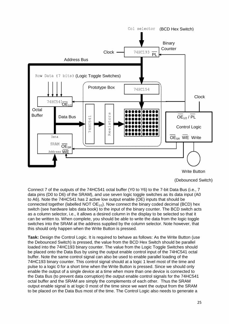
The next part of this experiment is to add some control logic to allow values to be written into the SRAM. The complete circuit should look something like this:
Prototype Box
Data Bus
Binary
Counter Clock
Array Row
Inputs
Array Column
Inputs
25
Connect 7 of the outputs of the 74HC541 octal buffer (Y0 to Y6) to the 7-bit Data Bus (i.e., 7 data pins (D0 to D6) of the SRAM), and use seven logic toggle switches as its data input (A0 to A6). Note the 74HC541 has 2 active low output enable (OE) inputs that should be connected together (labelled NOT OE1/2). Now connect the binary coded decimal (BCD) hex switch (see hardware labs data book) to the input of the binary counter. The BCD switch acts as a column selector, i.e., it allows a desired column in the display to be selected so that it can be written to. When complete, you should be able to write the data from the logic toggle switches into the SRAM at the address supplied by the column selector. Note however, that this should only happen when the Write Button is pressed.
Task: Design the Control Logic. It is required to behave as follows: As the Write Button (use the Debounced Switch) is pressed, the value from the BCD Hex Switch should be parallel loaded into the 74HC193 binary counter. The value from the Logic Toggle Switches should be placed onto the Data Bus by using the output enable control input of the 74HC541 octal buffer. Note the same control signal can also be used to enable parallel loading of the 74HC193 binary counter. This control signal should at a logic 1 level most of the time and pulse to a logic 0 for a short time when the Write Button is pressed. Since we should only enable the output of a single device at a time when more than one device is connected to the Data Bus (to prevent data corruption) the output enable control signals for the 74HC541 octal buffer and the SRAM are simply the complements of each other. Thus the SRAM output enable signal is at logic 0 most of the time since we want the output from the SRAM to be placed on the Data Bus most of the time. The Control Logic also needs to generate a
OESR
OE1/2 / PL
OESR
PL
OE1/2
WE
WE
Write
Write Button
(Debounced Switch)
Control Logic
Prototype Box
Data Bus
Address Bus
(BCD Hex Switch)
(Logic Toggle Switches)
Clock
Binary
Counter
Octal
Buffer
Clock

26
write enable control signal for the SRAM. This signal should have a similar form to that of the output enable generated for the 74HC541 octal buffer. That is it should be at logic 1 most of the time (i.e., the SRAM is being read) and should briefly pulse to a logic 0 to enable it to be written to. However, the SRAM write enable pulse should go to logic 0 after the 74HC541 octal latch enable signal and return to logic 1 before it. This will ensure the data on the Data Bus are stable during the SRAM write operation. This will also guarantee that the SRAM address inputs are also stable during the SRAM write operation since the 74HC541 octal latch enable signal is also the 74HC193 counter parallel load signal. So to summarise, the inputs to the Control Logic will be the clock and the Write Button. It needs to produce three outputs: (i) a pulse signal used to enable the output of the 74HC541 octal buffer and to enable parallel loading of the 74HC193 counter, (ii) an output enable signal for the SRAM (actually the complement of (i)), (iii) a write enable pulse for the SRAM. Start by producing a timing diagram showing the clock signal and the switch being pressed. Fill in what you want the outputs to do as the switch is pressed and goes to logic 1. The Control Logic can be implemented using a 74HC74 dual D-type flip-flop (FF) and a 74HC00 quad 2-input NAND gate.
Tips:
Connect the Write Button (i.e., the Debounced Switch) to the D input of a D-type FF (2 are available on the 74HC74).
The second D-type FF can be connected in a shift register arrangement with the first one (mentioned in the previous tip) and the NAND gates can be used to generate the required control signals using the FF outputs as their inputs.
In order to write into the SRAM, make sure you satisfy the timing requirements on the SRAM write enable input as highlighted in the previous paragraph
The load of the binary counter is asynchronous. The output value changes immediately, and does not wait for the next rising edge of the clock.
The BCD hex switch (i.e., the column selector) needs 4 x 4K7 pull-down resistors on its 4 outputs. See hardware labs data book.
You might like a demonstrator to check before proceeding to the final design.
Assessment
Ticking criteria: Write up your experimental data and final design, and then answer the following questions. Demonstrate that your circuit works correctly: you should be able to specify a column on the LED array with the column selector and the data pattern for that column with the toggle switches. Pressing the write button should make the pattern permanent.
Once your work has met the Common Ticking Criteria (see Introduction), get your work ticked by an assessor. Remember that you need to hand in this assessed exercise as part of your portfolio of work (see the Head of Department's notice). Note: One tick is for completing steps 1 and 2 and the other for step 3 and answering the questions.
Questions
1. Each LED in the matrix can draw a maximum current of 5mA. What is the maximum current that the two LED arrays can draw during the operation of the frame store? 2. What would happen if the write button was not synchronised? © 2011 DJ Greaves, DL Gordon, SW Moore and IJ Wassell Page last updated on 10-Jun-2015
27
Workshop Five – nMOS, pMOS and CMOS Inverters
Introduction
In this workshop you will build nMOS, pMOS and CMOS inverters and then measure their characteristics.
Components
oscilloscope 1A prototyping box connecting wire pair of matched nMOS (ZVN3306A) and pMOS (ZVP2106A) FETs
27 4704.7k resistors 330nF capacitor
Step 1: Characterise nMOS Inverters
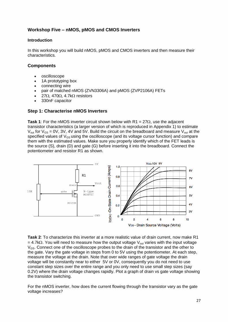
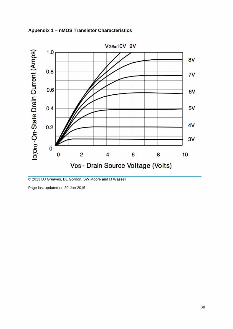
Task 1: For the nMOS inverter circuit shown below with R1 = 27, use the adjacent transistor characteristics (a larger version of which is reproduced in Appendix 1) to estimate Vout for VGS = 0V, 3V, 4V and 5V. Build the circuit on the breadboard and measure Vout at the specified values of VGS using the oscilloscope (and its voltage cursor function) and compare them with the estimated values. Make sure you properly identify which of the FET leads is the source (S), drain (D) and gate (G) before inserting it into the breadboard. Connect the potentiometer and resistor R1 as shown.
Task 2: To characterize this inverter at a more realistic value of drain current, now make R1
= 4.7k. You will need to measure how the output voltage Vout varies with the input voltage VGS. Connect one of the oscilloscope probes to the drain of the transistor and the other to the gate. Vary the gate voltage in steps from 0 to 5V using the potentiometer. At each step, measure the voltage at the drain. Note that over wide ranges of gate voltage the drain voltage will be constantly near to either 5V or 0V, consequently you do not need to use constant step sizes over the entire range and you only need to use small step sizes (say 0.2V) where the drain voltage changes rapidly. Plot a graph of drain vs gate voltage showing the transistor switching.
For the nMOS inverter, how does the current flowing through the transistor vary as the gate voltage increases?
R1
28
Task 3: Investigate the effect of capacitive loading. To do this include a 330nF capacitor (C) at the output of the nMOS inverter, i.e., connect it between Vout and GND (OV). Disconnect the potentiometer from the input VGS and instead connect VGS to the Clock Generator output. Set the operating frequency to say 100Hz initially, but be prepared to change it if required later on when performing measurements of output transition times. Sketch the input and output signals observed using the oscilloscope. Specifically, for the output rising edges measure the time it takes for the signal to rise from 0V to 0.63*5V = 3.15V and compare this with the time constant CR1. Now for the output falling edges, measure the time it takes for the signal to fall from 5V to 0.37*5V = 1.85V. Why is this much shorter than the rise time? Now estimate the ON resistance of the FET.
Now make R1 = 470andthen repeat the previous measurements. What is the advantage and what is the disadvantage of increasing R1?
Step 2: Investigate pMOS Inverters
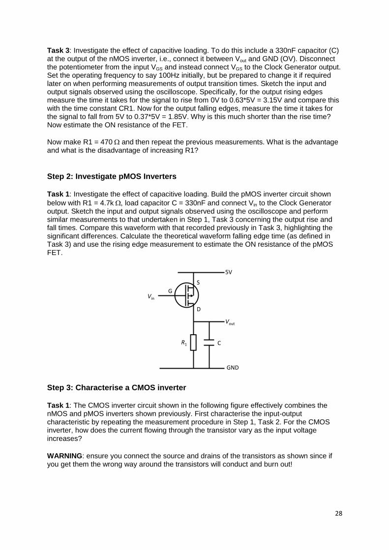
Task 1: Investigate the effect of capacitive loading. Build the pMOS inverter circuit shown
below with R1 = 4.7k load capacitor C = 330nF and connect Vin to the Clock Generator output. Sketch the input and output signals observed using the oscilloscope and perform similar measurements to that undertaken in Step 1, Task 3 concerning the output rise and fall times. Compare this waveform with that recorded previously in Task 3, highlighting the significant differences. Calculate the theoretical waveform falling edge time (as defined in Task 3) and use the rising edge measurement to estimate the ON resistance of the pMOS FET.
Step 3: Characterise a CMOS inverter
Task 1: The CMOS inverter circuit shown in the following figure effectively combines the nMOS and pMOS inverters shown previously. First characterise the input-output characteristic by repeating the measurement procedure in Step 1, Task 2. For the CMOS inverter, how does the current flowing through the transistor vary as the input voltage increases?
WARNING: ensure you connect the source and drains of the transistors as shown since if you get them the wrong way around the transistors will conduct and burn out!
R1
Vout
5V
GND
Vin
C
S
G
D

29
Task 2: Investigate the effect of capacitive loading. To do this add a 330nF capacitor (C) at the output, i.e., connect it between Vout and GND (OV). Disconnect the potentiometer from the inverter input and instead connect the inverter input to the Clock Generator output. Set the operating frequency to say 100Hz initially, but be prepared to change it if required later on when performing measurements of output transition times. Sketch the input and output signals observed using the oscilloscope. Compare this waveform with those observed previously for the nMOS and pMOS inverters and note down the significant differences. What other advantage does the CMOS inverter have over the nMOS and pMOS inverters?
Assessment
Ticking criteria: Write up your experimental data and answer the questions.
Once your work has met the Common Ticking Criteria (see Introduction), get your work ticked by an assessor. Remember that you need to hand in this assessed exercise as part of your portfolio of work (see the Head of Department's notice).
30
Appendix 1 – nMOS Transistor Characteristics
© 2013 DJ Greaves, DL Gordon, SW Moore and IJ Wassell Page last updated on 30-Jun-2015
31
Workshop Six - Digital-to-Analogue Conversion
Introduction
In this workshop, you will build two different kinds of digital-to-analogue converter (DAC). The first uses a resistor network called an R2R ladder, and it works in parallel, i.e., a binary value is fed into the resistor network in parallel and a corresponding analogue signal is output. The second DAC (known as a 1-bit DAC) is all digital and uses a clock and a state machine to produce a single output. The output passed through an analogue low pass filter (LPF) that removes the high frequency digital component leaving an average of the ones and zeros as the analogue output. The more ones that are in the data sequence at the LPF input will cause the output voltage to rise, while the more zeros will cause the output voltage to fall.
Components
1A prototyping box
1 x 110 resistor
6 x 4k7 resistors 1 x 74HC283 adder 1 x 74HC374 octal D-type flip-flop
1 x 0.1F capacitor 1 x light bulb and holder nMOS FET (ZVN3306A)
Step 1: R2R ladder DAC
Task 1: Consider the following resistor network and answer questions 1 and 2.
Task 2: Now consider the inverted version of this resistor network and answer question 1 again.
Step 2: Build the R2R DAC
Task 1: Construct the inverted DAC using 4.7k resistors to replace the 2 resistors, and
two 4.7k resistors in parallel to replace the 1 resistors. Use the toggle switches as input and check that the output voltages are correct as the inputs are changed.
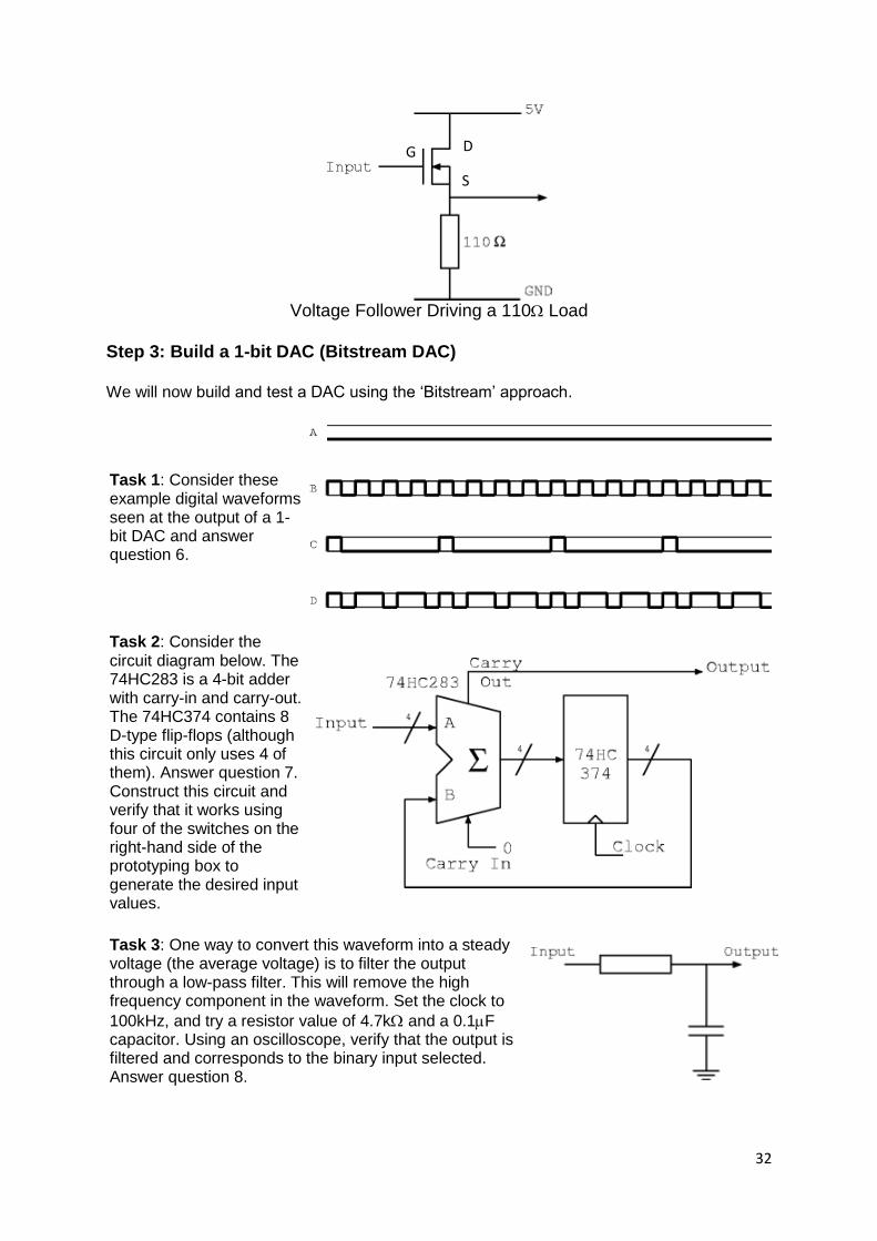
Task 2: Now connect an nMOS transistor and resistor load to form a voltage follower as shown in the following figure. Answer questions 3, 4 and 5.
32
Voltage Follower Driving a 110 Load
Step 3: Build a 1-bit DAC (Bitstream DAC)
We will now build and test a DAC using the ‘Bitstream’ approach.
Task 1: Consider these example digital waveforms seen at the output of a 1-bit DAC and answer question 6.
Task 2: Consider the circuit diagram below. The 74HC283 is a 4-bit adder with carry-in and carry-out. The 74HC374 contains 8 D-type flip-flops (although this circuit only uses 4 of them). Answer question 7. Construct this circuit and verify that it works using four of the switches on the right-hand side of the prototyping box to generate the desired input values.
Task 3: One way to convert this waveform into a steady voltage (the average voltage) is to filter the output through a low-pass filter. This will remove the high frequency component in the waveform. Set the clock to
100kHz, and try a resistor value of 4.7k and a 0.1F capacitor. Using an oscilloscope, verify that the output is filtered and corresponds to the binary input selected. Answer question 8.
G D
S
33
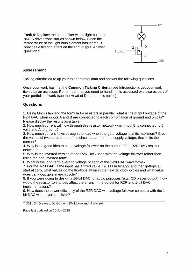
Task 4: Replace the output filter with a light bulb and nMOS driver transistor as shown below. Since the temperature of the light bulb filament has inertia, it provides a filtering effect on the light output. Answer question 9.
Assessment
Ticking criteria: Write up your experimental data and answer the following questions.
Once your work has met the Common Ticking Criteria (see Introduction), get your work ticked by an assessor. Remember that you need to hand in this assessed exercise as part of your portfolio of work (see the Head of Department's notice).
Questions
1. Using Ohm's law and the formula for resistors in parallel, what is the output voltage of the R2R DAC when inputs A and B are connected to each combination of ground and 5 volts? Please display the results as a table. 2. How much current will flow through this resistor network when input B is connected to 5 volts and A to ground? 3. How much current flows through the load when the gate voltage is at its maximum? Give the values of two parameters of the circuit, apart from the supply voltage, that limits the current? 4. Why is it a good idea to use a voltage follower on the output of the R2R DAC resistor network? 5. Why is the inverted version of the R2R DAC used with the voltage follower rather than using the non-inverted form? 6. What is the long-term average voltage of each of the 1-bit DAC waveforms? 7. For the 1-bit DAC, if the input has a fixed value 7 (0111 in binary), and the flip-flops all start at zero, what values do the flip-flops attain in the next 16 clock cycles and what value does carry-out take in each cycle? 8. If you were going to design a 16-bit DAC for audio purposes (e.g., CD player output), how would the resistor tolerances affect the errors in the output for R2R and 1-bit DAC implementations? 9. How does the power efficiency of the R2R DAC with voltage follower compare with the 1-bit DAC with driver transistor?
© 2011 DJ Greaves, DL Gordon, SW Moore and IJ Wassell Page last updated on 10-Jun-2015
G D
S