Embed Size (px)
Citation preview

2015 Packaging SymposiumNov. 2015
Kyocera America
1
Organic Interposer and Embedded SubstrateOrganic Interposer and Embedded Substrate
Tomoyuki Yamada
Sr. Field Applications Engineer
Kyocera America Inc.
1401 Rt 52, Suite 203, Fishkill, NY 12524
2015 Packaging SymposiumNov. 2015
Kyocera America
Created by S. Osako
All rights reserved
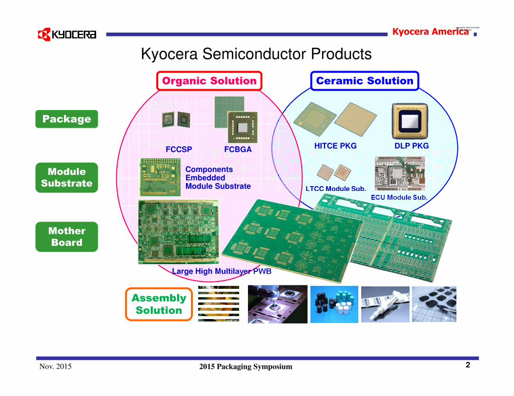
Package
FCCSP FCBGA
Large High Multilayer PWB
LTCC Module Sub.
ComponentsEmbedded Module Substrate
Module
Substrate
Mother
Board
Organic Solution Ceramic Solution
Assembly
Solution
ECU Module Sub.
HITCE PKG DLP PKG
Kyocera Semiconductor Products
Created by Seiichiro Osako
All rights reserved
2
2015 Packaging SymposiumNov. 2015
Kyocera America
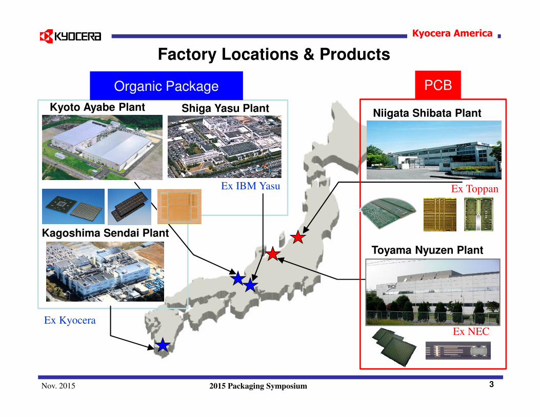
Factory Locations & Products
Toyama Nyuzen Plant
Niigata Shibata Plant
Kagoshima Sendai Plant
PCBOrganic Package
Kyoto Ayabe Plant Shiga Yasu Plant
Ex IBM Yasu
Ex KyoceraEx NEC
Ex Toppan
3

2015 Packaging SymposiumNov. 2015
Kyocera America
FeaturesFeatures
•Low Composite CTE
•No Limitation of Body Size
•High Density Design Rules
•Assembly Friendly
•Low Insertion Loss, Zo Matching
Applications Applications
Advanced Features of APX Advanced Features of APX
•2.5D Interposer
•Chip Scale Package
•Multi-Chip Module
•High Bandwidth Memory, Wide I/O Memory
Memory
MemoryMemory
Logic Chip
APX interposer
Substrate
MemoryMemoryMemory
Fine Pitch Flip Chip Pitch Stacked Micro Vias Fine Line & Space Fine Pitch Through Hole
4
Organic Interposer
2015 Packaging SymposiumNov. 2015
Kyocera America
5
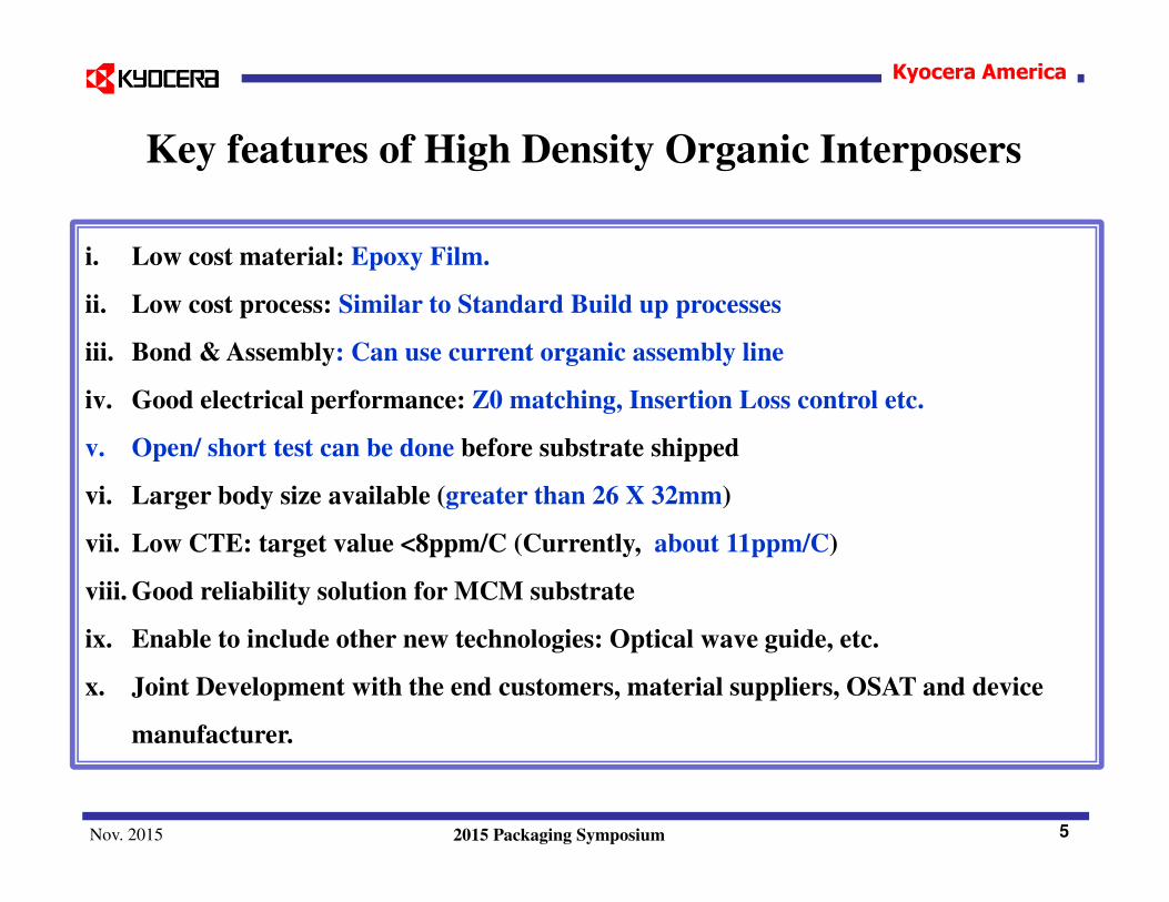
Key features of High Density Organic Interposers
i. Low cost material: Epoxy Film.
ii. Low cost process: Similar to Standard Build up processes
iii. Bond & Assembly: Can use current organic assembly line
iv. Good electrical performance: Z0 matching, Insertion Loss control etc.
v. Open/ short test can be done before substrate shipped
vi. Larger body size available (greater than 26 X 32mm)
vii. Low CTE: target value <8ppm/C (Currently, about 11ppm/C)
viii. Good reliability solution for MCM substrate
ix. Enable to include other new technologies: Optical wave guide, etc.
x. Joint Development with the end customers, material suppliers, OSAT and device
manufacturer.
2015 Packaging SymposiumNov. 2015
Kyocera America
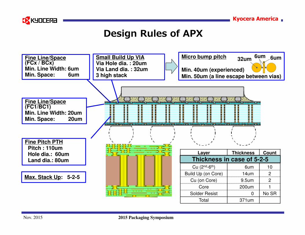
6666
Small Build Up VIAVia Hole dia. : 20umVia Land dia. : 32um3 high stack
Fine Line/Space (FCx / BCx)Min. Line Width: 6umMin. Space: 6um
Fine Line/Space (FC1/BC1)Min. Line Width: 20umMin. Space: 20um
Max. Stack Up: 5-2-5
Micro bump pitch
Min. 40um (experienced)
Min. 50um (a line escape between vias)
6um6um32um
Fine Pitch PTHPitch : 110umHole dia.: 60umLand dia.: 80um
Layer Thickness Count
Build Up (2nd-5th) 8um 8
Cu (2nd-6th) 6um 10
Build Up (on Core) 14um 2
Cu (on Core) 9.5um 2
Core 200um 1
Solder Resist 0 No SR
Total 371um
Thickness in case of 5-2-5
Design Rules of APX

2015 Packaging SymposiumNov. 2015
Kyocera America
Line & Space Micro Via Pitch &
DiameterCTE Z0 matching
Dielectric Film Thickness
10um
8um
6um
5um
4um
3um
2um
1um
12ppm
10ppm
9ppm
8ppm
5ppm
12um
10um
8um
5um
3um
Development of Fine Patterning Technology
Pitch: 55um
Pitch: 40um
UnderDevelopment
EstablishElemental
TechnologyMarch 2015
Pitch: ≦40umφφφφ 15 um
φφφφ 20 um
φφφφ 20 um
DevelopmentDone
DoneAssembleReliability
DevelopmentDone
DoneAssembleReliability
UnderDevelopment
EstablishElemental
Technology2015
DevelopmentDone
DevelopmentDone
UnderDevelopment
EstablishElemental
Technology2015
DevelopmentDone
DevelopmentDone
7
2015 Packaging SymposiumNov. 2015
Kyocera America
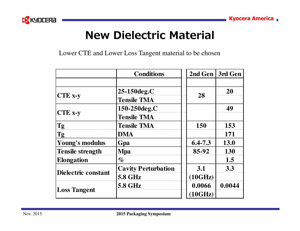
New Dielectric Material
Conditions 2nd Gen 3rd Gen
25-150deg.C 20
Tensile TMA
150-250deg.C 49
Tensile TMA
Tg Tensile TMA 150 153
Tg DMA 171
Young's modulus Gpa 6.4-7.3 13.0
Tensile strength Mpa 85-92 130
Elongation % 1.5
Cavity Perturbation 3.1 3.3
5.8 GHz (10GHz)
5.8 GHz 0.0044
CTE x-y
0.0066
(10GHz)Loss Tangent
Dielectric constant
28
CTE x-y
Lower CTE and Lower Loss Tangent material to be chosen

2015 Packaging SymposiumNov. 2015
Kyocera America
APX interposer
50um Pitch Test Die
MemorySize : 5x10mm
Size : About 20mmASIC
50um Pitch Test Die
Multi-Chip Package
Example of Internal Evaluation Test Vehicles
2.5D Interposer & Daughter Card
9
Qualification Test Condition
WTC (-65/150degC; 400cycles)
DTC (-55/125degC; 1000cycles)
HAST(130degC,85%, 3.7V; 288hrs)
THB (85degC,85%,5V, 1000hrs)
2015 Packaging SymposiumNov. 2015
Kyocera America
10
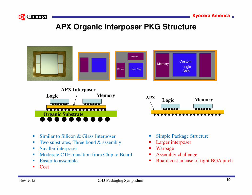
APX Organic Interposer PKG Structure
Logic Chip
Memory
Memory
Custom
LogicChip
Memory
APXLogic
APX Interposer
Organic Substrate
MemoryLogic Memory
� Similar to Silicon & Glass Interposer
� Two substrates, Three bond & assembly
� Smaller interposer
� Moderate CTE transition from Chip to Board
� Easier to assemble.
� Cost
� Simple Package Structure
� Larger interposer
� Warpage
� Assembly challenge
� Board cost in case of tight BGA pitch

2015 Packaging SymposiumNov. 2015
Kyocera America
APX Technology Roadmap
2015 2016 2017
Core Layer Number of Layer 2 2 2
Min Line/ Space (um) 20/20 15/15 15/15
Core Thickness (um) 200 200 / 150 200 / 150
PTH Land/Pitch (um) 80/110 65 / >80 65 / >80
Build Up Layer
Build up Material Gen2 Gen2Gen3 Gen3
Number of Build up Layer 5 5 6
Min. Line/ Space (um) 6/6 5/5 5/5
Conformal VIA Hole/Land (um) 33/50 33/50 33/50
Filled VIA Hole/Land (um) 20/32 20/32 20/32
Number of Via stack 3 3 3
Build UpLayer
Next Gen.
Build up Material T.B.D.
Number of Build up Layer 3
Min. Line/ Space (um) 3/ 3
Conformal VIA Hole/Land (um) 20/32
Filled VIA Hole/Land (um) 15/25
Number of Via stack 2
2015 Packaging SymposiumNov. 2015
Kyocera America
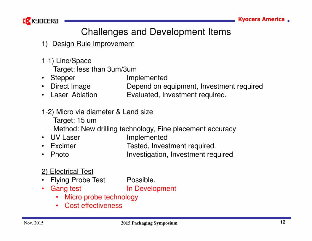
Challenges and Development Items
12
1) Design Rule Improvement
1-1) Line/Space
Target: less than 3um/3um
• Stepper Implemented
• Direct Image Depend on equipment, Investment required
• Laser Ablation Evaluated, Investment required.
1-2) Micro via diameter & Land size
Target: 15 um
Method: New drilling technology, Fine placement accuracy
• UV Laser Implemented
• Excimer Tested, Investment required.
• Photo Investigation, Investment required
2) Electrical Test
• Flying Probe Test Possible.
• Gang test In Development
• Micro probe technology
• Cost effectiveness

2015 Packaging SymposiumNov. 2015
Kyocera America
Embedded components technology
Puncher
Available for prototype and small production of active components, passive components embedded substrate.
Mounter
Die bonder
core board
opening component insertion
Micro via jointBuild layer formationcomponent mounting
Active component(WLP)
Embedded WLP
Embedded C/R
Passive component(C/R)
Embedded component PCB(Active die on base plate)
Embedded component PCB(Active die and Passeive in core)

2015 Packaging SymposiumNov. 2015
Kyocera America
Process Flow: One in One VS Two in One
Core board Opening Component insertion
Component(ex. C/R)
Carrier filmattaching
Resin filling,Resin curing,Removing carrier film
Core board Lager opening Multi-componentinsertion
Standard Process (One in One Hole)
Multi Component Process(ex. Two Components in One Hole)
Two components
in one hole
Joint by via platingBuild layer formation
Embedded C/R
Carrier filmattaching
Resin filling,Resin curing,Removing carrier film
Joint by via platingBuild layer formation
2015 Packaging SymposiumNov. 2015
Kyocera America
X-section
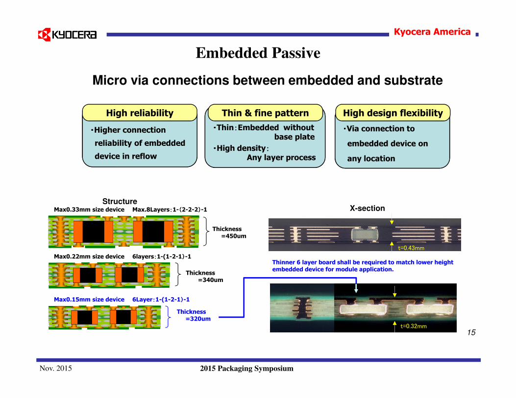
t=0.43mm
Max0.33mm size device Max.8Layers::::1-((((2-2-2))))-1
Max0.15mm size device 6Layer::::1-(1-2-1))))-1
Thickness =450um
Micro via connections between embedded and substrate
・・・・Higher connection
reliability of embedded
device in reflow
・・・・Thin::::Embedded without base plate
・・・・High density::::
Any layer process
・・・・Via connection to
embedded device on
any location
High reliability Thin & fine pattern High design flexibility
Structure
t=0.32mm
Max0.22mm size device 6layers::::1-(1-2-1))))-1Thinner 6 layer board shall be required to match lower height embedded device for module application.
Thickness =340um
Thickness =320um
15
Embedded Passive

2015 Packaging SymposiumNov. 2015
Kyocera America
1-0-1 Type
Dielectric Conductor
Nominal : 380µm
Designed Value
(Thickness)
25µm25µm
40µm
0µm
200µm
8µm
32µm25µm
25µm
L2
L1
L3
L4
Phase 1. Copper post + via Phase 2. No Base Plate
•Thinner Total thickness
PCB thickness :0.73(±0.10)mm
P.P.
LSI
ChipDielectric
Laser Via
Embedded Active
2-3-21-(2)-1Thickness: 0.38(±0.04)mm
Core
PCB thickness :0.73(±0.10)mm
Proto typing nowVolume Production
Application: SiP, RF module,
2015 Packaging SymposiumNov. 2015
Kyocera America
Summary
• Sampling of organic interposer available with HBM and Wide I/O.
– Organic interposer on board
– Organic interposer on daughter card
• Bond and assembly evaluation & reliability test in progress.
– Working with multiple chip suppliers and system houses.
• Embedded substrates are in qualification.
– Embedded DIE
– Embedded Passive
17
2015 Packaging SymposiumNov. 2015
Kyocera America
Thank you for your attention
Any questions?
18