Embed Size (px)
Citation preview
1
© Fraunhofer IPMS Bernd Richter/ 2010 -10
Highly-efficient embedded organic light emitter for CMOS optoelectronics
Bernd Richter, Uwe Vogel, Karsten Fehse, Rigo Herold, Thomas Presberger, Stephan Brenner, Lars Kroker
Fraunhofer IPMS - Center for Organic Materials and Electronic Devices Dresden COMEDD
© Fraunhofer IPMSBernd Richter/ 2010 -10
Outline
� Introduction
� OLED-on-CMOS: Applications
� OLED Microdisplays
� Technology
� Conclusion
© Fraunhofer IPMSBernd Richter/ 2010 -10
transparent conductor
organic layers
metal cathode
substrate
Light emission +_
bottom-emitting top-emitting
Light emission
(silicon wafer)
Introduction to organic LEDs - OLEDs
� Lighting
� Medium and large display ⇒ TFT
� OLED-on-CMOS
© Fraunhofer IPMSBernd Richter/ 2010 -10
Introduction: OLED-on-CMOS (1)
Top-emitting p-i-n OLED:
� highly-efficient OLED light sourcein/on CMOS
� based on small molecules(NOVALED AG)
� evaporated on Si-wafer
� sub-structuring by shadow mask >100µm
� all colors monochrome, white, NIR
� doped charge transport layers
� low operating voltage
� transparent top electrode
� extremely thin (~100...300nm)
� excellent current and
power efficiency(low-voltage, low-power)
� fast response time (MHz)-5 -4 -3 -2 -1 0 1 2 3 4 5
10-6
10-5
10-4
10-3
10-2
10-1
100
101
102
101
102
103
104
105
orange emitter
red emitter white emitter system
Cu
rren
t de
nsity [
mA
/cm
²]
Voltage [V]
Lu
min
an
ce
[c
d/m
²]
5.7
11.6
14.1
Current
efficiency[Cd/A]
@100cd/m²
4.73.2white
12.0003.22.5ora
3.12.4red
@1000cd/m²
@100cd/m²
lifetime
@1000c
d/m²
Voltage [V]
(+)
(-)

2
© Fraunhofer IPMSBernd Richter/ 2010 -10
Introduction: OLED-on-CMOS (2)
� CMOS top metal = OLED bottom electrode
� top metal definesOLED shape
� arbitrary shapes
� driving circuitry
underneath
Wafer
FOX
PMOS Photodiode
Metal 1
Metal 2
Metal 3
CMOS
OLED
TFE
CMOS cross-section with OLED on top
� CMOS integration of electronic features
� driving
� acqusition
� processing
� control
� Co-integration of CMOS-compatible sensors
� embedded photodetectors
� temperature
� magnetic (Hall)
� MEMS,...
© Fraunhofer IPMSBernd Richter/ 2010 -10
Example: OLED-on-CMOS testchip
1.3 mm
2 µm
4 µm
� no active circuit, hardwired pattern (3 metals)
� separate deposition of monochrome RGB-OLED (shadow mask)
� pixel sub-structuring: shape of CMOS top metal
~60 mm
© Fraunhofer IPMSBernd Richter/ 2010 -10
Outline
� Introduction
� OLED-on-CMOS: Applications
� OLED Microdisplays
� Technology
� Conclusion
© Fraunhofer IPMSBernd Richter/ 2010 -10
OLED-on-CMOS: Applicationssensors
� optical sensors
� fluorescence, color, flowmetry, photoplethysmography,...
� light barriers (reflective)
� embedded illumination for image sensors
� patterned illumination possible
� optical finger-print, lab-on-chip,...
� opto-coupler
microdisplays
� microdisplay
� HMD, mobile/micro-projection, electronic viewfinder,...
� bidirectional microdisplay(display + embedded image sensor)
� interactive HMD
� optical inspection,...
iiii ARARARAR
OLED CM OS DetektorOLED CM OS Detektor
3
© Fraunhofer IPMSBernd Richter/ 2010 -10
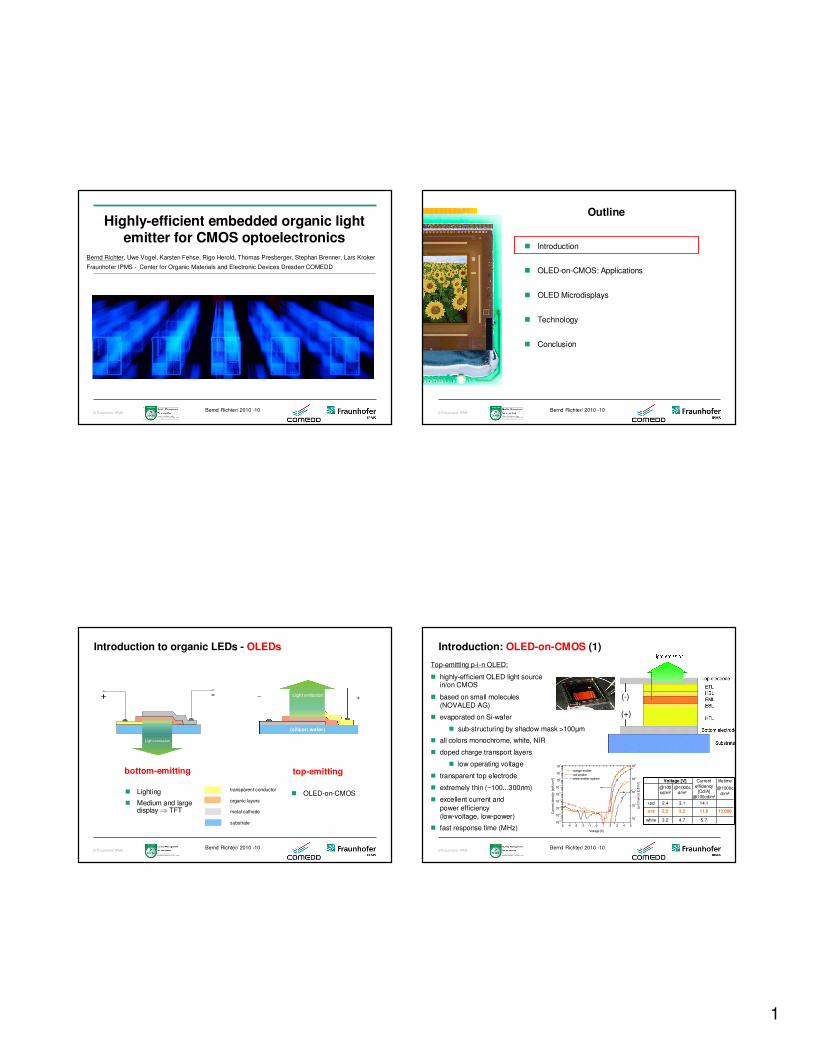
OLED-on-CMOS: Sensors
� CMOS photodetectors (PD) and embedded OLED illumination, excitation
� three types of optoelectronic sensors:
� reflection light barrier (top left)
� flow sensor (bottom left)
� color sensor (right)
� circuitry underneath OLED electrodes
10,5
3,5PD
PD
PD PD
PD
OLEDRed
OLEDBlue
OLEDGreen
OLEDNIRPDPD PD PD PDPD PDPD
OL ED1
OLED2
PD PD
OLEDPDOLED PD PD PDPD
© Fraunhofer IPMSBernd Richter/ 2010 -10
OLED-on-CMOS: Sensor applications
� Particle flow sensor
� OLED stripes for fluid illumination and 8 photodiodes
� light reflection depending on local fluid velocity and particle density
� analyzing photocurrents and correlation functions, the fluid particle velocity can be calculated
� Opto-coupler
OLED Photodiodes
Encapsulation
CMOS Chip
Capillary with flowing transparentfluid and reflecting particles
© Fraunhofer IPMSBernd Richter/ 2010 -10
Outline
� Introduction
� OLED-on-CMOS: Applications
� OLED Microdisplays
� Technology
� Conclusion
© Fraunhofer IPMSBernd Richter/ 2010 -10
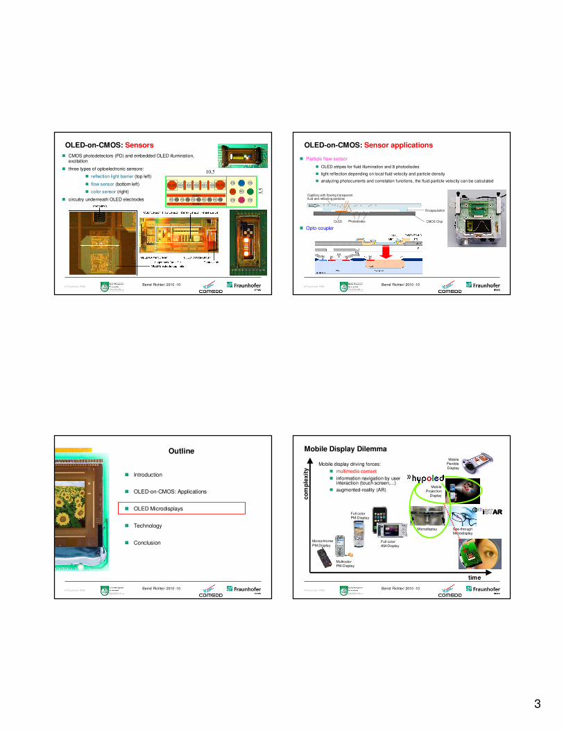
time
co
mp
lexit
y
Monochrome
PM-Display
MulticolorPM-Display
Full colorPM-Display
Full colorAM-Display
Microdisplay See-throughMicrodisplay
MobileProjection
Display
MobileFlexible
Display
iiii ARARARAR
Mobile display driving forces:
� multimedia content
� information navigation by user interaction (touch screen,...)
� augmented-reality (AR)
Mobile Display Dilemma

4
© Fraunhofer IPMSBernd Richter/ 2010 -10
OLED microdisplay: Overview
line
dri
ver
data driver
video input, control
RGB pixel
data supply
OLED microdisplay
� Physically very small, but
� high information content (TV quality)
� low power consumption
� enlarged image viewed through magnifying optics
� Active-matrix substrate
� data is stored inside pixel: analog/digital
� sub-pixel size: {(4x4), 4x12, 8x8, 36x36} µm²
� OLED pixel current: pA...nA
� sub-structuring of display pixel withmonochrome colors not possible
� combination of white OLEDs with colour filter
� Applications
� projection (rear, front, micro)
� near-to-eye (NTE)
� electronic viewfinder
� head mounted
© Fraunhofer IPMSBernd Richter/ 2010 -10
OLED microdisplay: Pixel concept
� small pixel pitch (≤12um RGB)
� OLED: current driven pA...nA, Lum~ioled
� grayscale realization: analog / digital
Increased number
of transistors
- no D/A
conversion
- stable storage of bits
digital SRAM pixel cell
many transistors + DRAM refresh
necessary
- no D/A
conversion
- simple linearity
correction by PWM
digital DRAM pixel cell
pixel cell transistor matching is
important
shortprogramming
duration
voltage programmed
long programming
duration due to
small currents
pixel cell
transistor
matching is irrelevant
current programmed
(+subthreshold
scaling)
DisadvantageAdvantagePixel Cell Principle
„ZOOM“
iiii ARARARAR
an
alo
gd
igita
l
Dd
ata
display pixel
Md1
sa
cat
Md2Md3
Md4
OLED
Cd
em
vref
© Fraunhofer IPMSBernd Richter/ 2010 -10
OLED microdisplay: Hypoled
� full color VGA (640x480) OLED microdisplay
� pixel cell
� digital DRAM pixel cell
� luminance control by PWM
� sub-pixel: 4x12µm²
� 24 bit parallel video interface
� 50/60Hz frame rate
� configuration of color, contrast and gamma correction via I²C
� high brightness
� up to 10,000 nits for monochrome green (micro-projection)
� 1,000 nits for RGB color (HMD)
� 0.18µm CMOS foundry process
� core supply, digital I/O interface 1.8V
� negative OLED cathode voltage (max. -5.5V)
� active area 7.7x5.8mm²
� chip size 12x11mm²7.7mm
5.8
mm
© Fraunhofer IPMSBernd Richter/ 2010 -10
Hypoled : Applications
� head-mounted display (HMD)
� RGB micro-projector
MediaBox (DVB-T, DVB-H, WLAN)

5
© Fraunhofer IPMSBernd Richter/ 2010 -10
Bidirectional OLED microdisplay: Overview
OLED CMOS detector
CMOS wafer
CMOS circuit
encapsulation
micro-optics
"Bidirectional" functionality:
� OLED microdisplay + embedded image sensor
� nested display and camera pixel
� embedded CMOS photodiodes
� lower level than OLED
� side-by-side with active electronicsdevices
� local optical crosstalk possible
� emission and detection can be operated in parallel or sequentially
line d
river
data driver
video input, control
displaydata
OLED microdisplay
cam readout
line d
river
video output, control
camdata
embedded image sensor
bidirectional microdisplay
© Fraunhofer IPMSBernd Richter/ 2010 -10
Bidirectional OLED microdisplay: HMD appl.
53 km/h Radio
Navi
Me
nü
Display off
-1°
30
60
� conventional, unidirectional microdisplay
� displays an image
� OLED-on-CMOS microdisplay
� bidirectional microdisplay
� displays an image and detects anotherimage on the same device
� OLED-on-CMOS microdisplay + embeddedimage sensor
� HMD application: aimed at tracking the eyemovement with respect to
� user's sight (consciously and unconsciously)
� user's (situation) awareness (unconsciously)
� gaze-based human-display-interaction
� visual Input-/Output-Device (I/O) for personal information management (PIM)
� interactive augmented-reality (AR) applications
© Fraunhofer IPMSBernd Richter/ 2010 -10
Bidirectional see-through HMD
Applications
Automotive
� mission-critical information
� navigation
� safety (gaze monitoring)
Mobile Communication
� telecom
� mobile multimedia
� tourist information
Industry
� mobile maintenance
Medicine
� surgery support
Security
� disaster management
� mobile surveillance
� mission control
Thermocouples
Part No. 467-854
More Information
Yes No ?
SMS by " BOSS" :(Wed, 05/02/14, 18:21)
Hi Paul,
how about our meet ing today?
Have you missed i t? Please
cal l back immediately!
Rgds, BOSS.
CALL DEL ESC
OT: 5:35
SPL: 60dB
BP : 40/105
F: 23mN
HR: 93
SPL
CT: 14:21
LAS MOB
f: 1kHz
© Fraunhofer IPMSBernd Richter/ 2010 -10
Bidirectional OLED microdisplay: 1st prototype “ZOOM”
OLED-Microdisplay
� Resolution monochrome QVGA (320 x 240)
� Grayscale 8 Bit, datainterface digital
� Pixel analog, pitch 36µm
� Peak luminance adj.: 100...20.000cd/m2
� Viewing area 11,5 x 8,6mm²
� Chipsize 18.7x16.4mm²
Image sensor
� Resolution 160x120 pixels (QQVGA)
� Photoactive area 8x8µm², linear readout
� Quickcapture I/F (w/ external ADC)
General
� Power Supply 3.3V
� OLED Supply-9..0V
� Configuration via I2C
� Samples in lab, eval. kit expected Q1/2011

6
© Fraunhofer IPMSBernd Richter/ 2010 -10
Bidirectional OLED microdisplay: ZOOM-HMD
� see-through HMD
� semitransparent mirror
� separate optical pathes for display (VIS) and camera (NIR) � filters
� PDA-like host with embedded computer
� embedded Linux
� image processing � eye-tracking
� user interfaces/interaction + app.
captured eye-scenevirtual image
© Fraunhofer IPMSBernd Richter/ 2010 -10
Bidirectional OLED microdisplay: "iSTAR"
Nested activematrix640x480 colored OLEDs
128x96 photodiodes
Column electronic
Readout electronic
Row
logic
Controllogic
Zeilenlogik
Bottom matrix (1280x40)
Row logic
Ro
w logic
Controllogic
Top matrix (1280x40)
Re
ado
ut ele
ctr
onic
Row logic
Pads
PD
Controllogic
Nested activematrix640x480 colored OLEDs
128x96 photodiodes
Column electronic
Readout electronic
Row
logic
Controllogic
Zeilenlogik
Bottom matrix (1280x40)
Row logic
Ro
w logic
Controllogic
Top matrix (1280x40)
Re
ado
ut ele
ctr
onic
Row logic
Pads
PDPD
Controllogic
iSTAR chip micro-photograph
13mm
11
mm
Display Nested camera Frame camera� full-color VGA 640x480
� Sub-pixel 8x8µm
� ≤1000 nits
� embedded/intersected camera
� 128x96 pixel
� frame camera
� top + bottom 1280x40
� microlenses
� interface display / camera
� parallel + sync signals
� configuration via I2C
� dimensions
� active area 10.2x7.7mm²
� chip size 13x11mm²
� volume-capable processes
� CMOS: 0.18µm (foundry)
� OLED: COMEDD pilot line
� first samples in lab, demo expected Q1/2011
© Fraunhofer IPMSBernd Richter/ 2010 -10
Outline
� Introduction
� OLED-on-Silicon: Sensor applications
� OLED Microdisplays
� Technology
� Conclusion
© Fraunhofer IPMSBernd Richter/ 2010 -10
IPMS-CMOSor external
CMOS foundry
CMOS-surfacemodification
(optional)
pin-OLEDPLED
deposition
thin film encapsulation
& colour filter
deposition
The whole process chain is available at COMEDD to
prepare OLED microdisplays.
dicing &assembly
OLED-on-CMOS: Manufacturing process flow

7
© Fraunhofer IPMSBernd Richter/ 2010 -10
SMALL MOLECULE pin-OLED DEPOSITION SYSTEM
SUNICEL PLUS200 @ IPMS
© Fraunhofer IPMSBernd Richter/ 2010 -10
Microdisplay components
CMOS-Wafer (200 mm)
Bond-pads
Display pixel covered with PLED or OLED
Transparent top-wafer (200 mm)
Encapsulation glue
Colour filter (RGB)
© Fraunhofer IPMSBernd Richter/ 2010 -10
Pre-Alignment of
CMOS to CF-wafer
Assembling in vacuum
Precise alignment of both wafer to
each other and UV-exposure of the encapsulation glue
Dicing and testing
Microdisplay production steps
© Fraunhofer IPMSBernd Richter/ 2010 -10
CMOSPixelpin-OLEDCathodeThin film encapsulationColour filter (optional)
Encapsulation glass
CMOS top metal (reverse currents
in OLEDs)
pin-OLED efficiency and lifetime
Oxygen and water barrier
400 500 600 7000.0
0.2
0.4
0.6
0.8
1.0
El-
Inte
ns
ity
(n
orm
.)
Wavelength (nm)
CracksPinholes in TFE
Cathode
Pinholes in Cathode
Inorganic multilayer
Organic
MAIN RESEARCH TOPICS FOR OLED MICRODISPLAYS

8
© Fraunhofer IPMSBernd Richter/ 2010 -10
Roll-to-Roll
Substrate size
Substrate type
Cycle time
Pilot max. volume
Substrates/ year
Pilot max.
volume area
Prototype/R&D
Ready for
Pilot production
Prototype lineRigid substrates
Pilot line
Rigid / Flexible
substrates
Pilot line
OLED-on-CMOS
200 x 200 mm2
Glass
120 minutes
Ready
370 x 470 mm2
(Generation2)
150 or 200 mm
diameter300 mm
width
Glass/laminated foil Si/CMOS wafer Metal foil
3 minutes 60 minutes
80,000 6000
13,000 m2
Ready Ready 2010
2010 2010
COMEDD EQUIPMENT FOR OLED AND OPV
© Fraunhofer IPMSBernd Richter/ 2010 -10
Outline
� Introduction
� OLED-on-Silicon: Sensor applications
� OLED Microdisplays
� Technology
� Conclusion
© Fraunhofer IPMSBernd Richter/ 2010 -10
Conclusion
� p-i-n type OLED on adapted TiN/Al electrodes well suitable forOLED-on-CMOS
� <5.0V @ 1000cd/m² → CMOS w/o HV option for high brightness
� co-embedded light sources, photodetectors, signal processing
� optical cross-coupling effects to be avoided
� opto-sensor applications
� patterned illumination/excitationand image/response detection/analysis
� fluorescence, color, opto-coupler
� lab-on-chip
� bidirectional OLED microdisplay
� display and image sensor in a single device
� eye-tracking in near-to-eye applications
� interactive head-mounted displays
� optical surface inspection
photodetectors
Si CMOS chip
carrier PCB
OLED
objectsurface
OLED CMOS detectorCMOS substrate (wafer) CMOS circuit
encapsulat ion
organic-opto-micro-system
micro-optics
© Fraunhofer IPMSBernd Richter/ 2010 -10
Acknowledgement
� Work was in parts sponsored by
� European Commission within the HYPOLED project
� Federal Ministry for Education and Research of the German government "ZOOM"
� Fraunhofer Internal Programs “iSTAR”
� Thanks to our collaborative project partners: X-FAB; Fraunhofer IOF, IOSB, IGD.
� Thanks to many more contributors at IPMS and our students!
Contact
� Bernd Richter (Fraunhofer IPMS)
� phone:+49-351-8823-285
� email: [email protected]
iiii ARARARAR
See demo during break!
Thank you for your attention!


![Lifetime reduction of a quantum emitter with quasiperiodic ...sspp.phys.tohoku.ac.jp/tomita/doc/paper/moritake14PRB.pdf · waveguides [19–22]. HMM is a highly anisotropic medium](https://img.dokumen.tips/doc/110x75/60e1837383eb1f5de9746381/lifetime-reduction-of-a-quantum-emitter-with-quasiperiodic-ssppphys-waveguides.jpg)