Embed Size (px)
Citation preview

N E W
Photon number resolving
qCMOS® camera C15550-20UP

With advances in electronmultiplication technology,
scientific cameras move from single photon counting toward
high QE/resolution imaging
Electron multiplication type With advances in sensor
technology, scientific cameras move toward high speed/resolution
Low noisetype
Readout noise15 electrons
Readout noise8 electrons
Readout noise1.5 electrons
Readout noise0.27 electrons
sCMOS cameraC11440 series
High-level cooled CCD cameraC3140, C3640
Low-noise cooled CCD cameraC4742 series ORCA®-Quest
PIASWorld's first photon counting camera
EB-CCD cameraC7190 series
EM-CCD cameraC9100 series
ICCD cameraC2400 series
*Readout noise is rms value.
1980s 1990s 2000s 2010s 2020s
The world’s first qCMOS® camera
camera evolutionThe dawn of a new era in scientific
Since the 1980s, Hamamatsu Photonics has continued to develop high-sensitivity, low-noise cameras using its unique camera design technology and has always contributed to the development of cutting-edge scientific and technological research. Now, in 2021, Hamamatsu Photonics are proud to release the ORCA®-Quest with ultimate performance.
Introducing the new ORCA®-Quest – a camera that achieves the ultimate in quantitative imaging.
The qCMOS® (Quantitative CMOS) is a CMOS image sensor that has the ability to detect and identify the number of both single and multiple photoelectrons.ORCA®-Quest is the world's first camera to incorporate the qCMOS® image sensor and to be able to resolve the number of photoelectrons using a newly developed dedicated technology. (See page 6)
Evolution from single photon counting to photon number resolving
What is qCMOS®?
2 3

Ultra-low readout noise 0.27 electrons rmsUltra-low readout noise 0.27 electrons rmsat Ultra quiet scanat Ultra quiet scan
qCMOS®
Gen III sCMOSGen II sCMOS
0.0001
0.001
0.01
0.1
1
Rel
ativ
e fre
quen
cy
Readout noise (electrons)
0 2 4 6 8 10
In order to detect weak light with high signal-to-noise, ORCA®-Quest has been designed and optimized to every aspect of the sensor from its structure to its electronics. Not only the camera development but also the custom sensor development has been done with latest CMOS technology, an extremely low noise performance of 0.27 electrons has been achieved.
Comparison of average 1 photon per pixel image (pseudo-color) Exposure time: 200 ms LUT: minimum to maximum value Comparison area: 512 pixels × 512 pixels
qCMOS® (ORCA®-Quest) Gen III sCMOS Gen II sCMOS
to achieve ultimate quantitative imagingthat enable the ORCA®-Quest Four key features
Extreme low-noise performance1.
Low-dark current 0.006 electrons/pixel/sLow-dark current 0.006 electrons/pixel/sat −35 °Cat −35 °C
In the field of single photon counting and photon number resolving, even dark currents as low as 0.5 electrons/pixel/s can affect photon detection. The 0.006 electrons/pixel/s @−35 °C value achieved by ORCA®-Quest is an extremely low probabilistic value of only 1 electron of dark current generated in approximately 167 pixels when exposed for 1 second.
Thus, the ORCA®-Quest, which is less affected by dark current, is ideal for quantitative imaging and analysis.
ORCA®-Quest Gen II sCMOS camera
Image quality comparison at long exposure time (pseudo-color) Incident light intensity: 0.05 photons/pixel/s Exposure time: 15 min (10 s × 90 times integration)
1. Extreme low-noise performance Realization of photon number resolving (PNR) output
2.
Realization of a large number of pixels and high speed readout
4.Back-illuminated structure and high resolution
3.
When performing long-time exposure, conventional EM-CCD cameras are easily affected by cosmic rays, and the resulting white spots have become a problem. ORCA®-Quest is not easily affected by cosmic rays and can suppress the deterioration of image quality due to white spots during long-time exposure.
Image quality comparison at long exposure time (pseudo-color)No incident light Exposure time: 30 min
ORCA®-Quest EM-CCD camera
4 5

Light is a collection of many photons. Photons are converted into electrons on the sensor, and these electrons are called photoelectrons. “Photon number resolving” is a method of accurately measuring light by counting photoelectrons.*
In order to count these photoelectrons, camera noise must be sufficiently smaller than the amount of photoelectron signal. Conventional sCMOS cameras achieve a small readout noise, but still larger than photoelectron signal, making it difficult to count photoelectrons.
Using advanced camera technology, the ORCA®-Quest counts photoelectrons and delivers an ultra-low readout noise of 0.27 electrons rms (@Ultra quiet scan), stability over temperature and time, individual calibration and real-time correction of each pixel value.
For more information about the qCMOS® image sensor, please refer to the ORCA®-Quest white paper.
* Photon number resolving is unique and quite different from photon counting (More precisely the method resolves the number of photoelectrons. However, since single photon counting instead of single photoelectron counting has been used for a comparable method in this field, we will use the term “photon number resolving” in this brochure).
Realization of photon number resolving by low-readout noiseRealization of photon number resolving by low-readout noise
Simulation data of photoelectron probability distribution (Average number of photoelectrons generated per pixel: 2 electrons)
Prob
abilit
y de
nsity
0.5
0.4
0.3
0.2
0.1
0.0
Photoelectron (electrons)
0 1 2 3 4 5 6 7 8
0.27 electrons0.50 electrons1.00 electrons1.50 electrons2.00 electrons
Readout noise
Realization of photon number resolving (PNR) output2.
to achieve ultimate quantitative imagingthat enable the ORCA®-Quest Four key features
Spatial photon number resolving capabilitySpatial photon number resolving capability
The graphs show simulated histograms when averaged photoelectrons are 3 and 10 electrons/pixel. While the EM-CCD and Gen II sCMOS cameras cannot realize the photon number resolving due to multiplication noise or higher readout noise, the ORCA®-Quest realizes spatial photon number resolving in addition to temporal photon number resolving.Furthermore, it follows Poisson distributions corresponding with averaged photoelectrons of 3 and 10 electrons/pixel.
Freq
uenc
y
0
2500
2000
1500
1000
500
Photoelectron (electrons)0 5 1510 20
Freq
uenc
y
600
500
400
300
200
0
100
250100 150 200Output Value (Digital Number)
0 5 1510 20Photoelectron (electrons)
Freq
uenc
y
25
20
15
10
0
5
50002000 3000 4000 6000Output Value (Digital Number)
0 5 1510 20Photoelectron (electrons)
Freq
uenc
y
1000
800
600
400
0
200
130100 110 120 140Output Value (Digital Number)
0 5 1510 20Photoelectron (electrons)
Average number of photoelectrons generated per pixel: 3 electrons
Freq
uenc
y
0
1400
1200
1000
800
600
400
200
0 5 1510 20Photoelectron (electrons) Output Value (Digital Number)
Freq
uenc
y
350
300
250
200
150
100
0
50
250100 150 200
0 5 1510 20Photoelectron (electrons)
Output Value (Digital Number)
0 5 1510 20Photoelectron (electrons)
Freq
uenc
y
600
500
400
300
200
0
100
130100 110 120 140Output Value (Digital Number)
0 5 1510 20Photoelectron (electrons)
Freq
uenc
y
50002000 3000 4000 6000
12
10
8
6
4
0
2
14
Average number of photoelectrons generated per pixel: 10 electrons
EM-CCD camera Gen II sCMOS camera ORCA®-Quest(Photon number resolving)
ORCA®-Quest(Ultra quiet scan)
Approx. 3 electrons/pixelApprox. 10 electrons/pixel
1. Extreme low-noise performance Realization of photon number resolving (PNR) output
2.
Realization of a large number of pixels and high speed readout
4.Back-illuminated structure and high resolution
3.
6 7

Trench structure to suppress crosstalkTrench structure to suppress crosstalk
High QE is essential for high efficiency of detecting photons and achieved by back-illuminated structure.
In conventional back-illuminated sensors, crosstalks occur between pixels due to no pixel separation, and resolutions are usually inferior to those of front-illuminated sensors. The ORCA®-Quest qCMOS®'s sensor has back-illuminated structure for achieving high quantum efficiency, and trench structure in one-by-one pixel for reducing crosstalk.
What is a trench structure?
Micro lens
Incident photon
Photodiode
Detection circuit
Trenchstructure
The trench structure suppresses the flow of photoelectrons to neighboring pixels.
qCMOS® image sensor cross-section
Enlarge
Photoelectron
Modulation Transfer Function (MTF) is a type of resolution evaluation. It is the value of how accurately the contrast of an object can be reproduced.
Measurement result of MTF
qCMOS®
Gen II sCMOS
Normalized Spatial Frequency
MTF
10.80.60.40 0.2
1
0.8
0.6
0.4
0
0.2
1.2
Back-illuminated structure and high resolution3.
to achieve ultimate quantitative imagingthat enable the ORCA®-Quest Four key features
High QE 90 % at 475 nm 33 % at 900 nmHigh QE 90 % at 475 nm 33 % at 900 nm
It also has high quantum efficiency in the near-infrared region because of its thicker layer of the charge detection region.
Normally, there is a trade-off between the thickness of the layer of the photon detection region and the resolution, but the trench structure suppresses the degradation of the resolution.
Etaloning-desensitizedEtaloning-desensitized
Etaloning is a phenomenon that occurs when the incident light interferes with the reflected light from the back surface of the silicon and causes varying sensitivity - dependent both on the spatial and the spectral position. In the case of an EM-CCD camera, it appears as a fringe pattern even with uniform monochrome light input, mostly in the IR.
The qCMOS® camera shows minimal etaloning compared to EM-CCD cameras.
EM-CCD
qCMOS®
(ORCA®-Quest)
800 nm 900 nm 1000 nm
Wavelength purity: 2 nm
1. Extreme low-noise performance Realization of photon number resolving (PNR) output
2.
Realization of a large number of pixels and high speed readout
4.Back-illuminated structure and high resolution
3.
0
10
20
30
40
50
60
70
80
90
100
Qua
ntum
effi
cien
cy (%
)
300 400 500 600 700 800 900 1000 1100
Wavelength (nm)
8 9
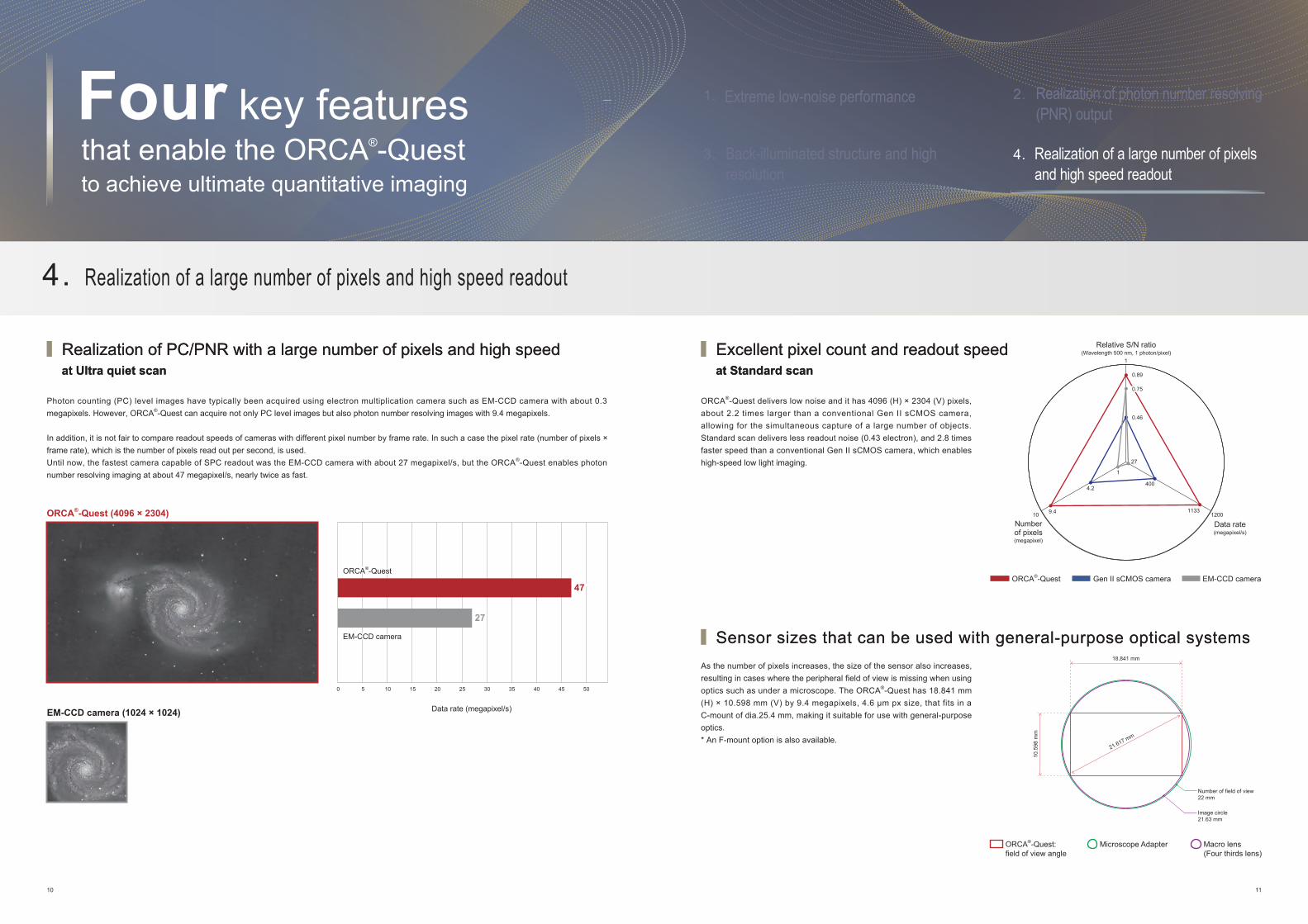
Realization of PC/PNR with a large number of pixels and high speedRealization of PC/PNR with a large number of pixels and high speedat Ultra quiet scanat Ultra quiet scan
Realization of a large number of pixels and high speed readout4.
Photon counting (PC) level images have typically been acquired using electron multiplication camera such as EM-CCD camera with about 0.3 megapixels. However, ORCA®-Quest can acquire not only PC level images but also photon number resolving images with 9.4 megapixels.
In addition, it is not fair to compare readout speeds of cameras with different pixel number by frame rate. In such a case the pixel rate (number of pixels × frame rate), which is the number of pixels read out per second, is used. Until now, the fastest camera capable of SPC readout was the EM-CCD camera with about 27 megapixel/s, but the ORCA®-Quest enables photon number resolving imaging at about 47 megapixel/s, nearly twice as fast.
0 5 10 15 20 25 30 35 40 45 50
Data rate (megapixel/s)
4747
2727
ORCA®-QuestORCA®-Quest
EM-CCD cameraEM-CCD camera
ORCA®-Quest (4096 × 2304)
EM-CCD camera (1024 × 1024)
to achieve ultimate quantitative imagingthat enable the ORCA®-Quest Four key features
at Standard scanat Standard scanExcellent pixel count and readout speedExcellent pixel count and readout speed
0.46
0.89
1
1200101133
4004.2
9.4
27
1
0.75
ORCA®-Quest delivers low noise and it has 4096 (H) × 2304 (V) pixels, about 2.2 times larger than a conventional Gen II sCMOS camera, allowing for the simultaneous capture of a large number of objects. Standard scan delivers less readout noise (0.43 electron), and 2.8 times faster speed than a conventional Gen II sCMOS camera, which enables high-speed low light imaging.
Sensor sizes that can be used with general-purpose optical systemsSensor sizes that can be used with general-purpose optical systemsAs the number of pixels increases, the size of the sensor also increases, resulting in cases where the peripheral field of view is missing when using optics such as under a microscope. The ORCA®-Quest has 18.841 mm (H) × 10.598 mm (V) by 9.4 megapixels, 4.6 μm px size, that fits in a C-mount of dia.25.4 mm, making it suitable for use with general-purpose optics.* An F-mount option is also available.
ORCA®-Quest: field of view angle
Microscope Adapter Macro lens (Four thirds lens)
18.841 mm
21.617 mm
10.5
98 m
m
Number of field of view22 mm
Image circle21.63 mm
ORCA®-Quest Gen II sCMOS camera EM-CCD camera
Relative S/N ratio(Wavelength 500 nm, 1 photon/pixel)
Numberof pixels(megapixel)
Data rate(megapixel/s)
1. Extreme low-noise performance Realization of photon number resolving (PNR) output
2.
Realization of a large number of pixels and high speed readout
4.Back-illuminated structure and high resolution
3.
10 11
Application and Measurement Examples
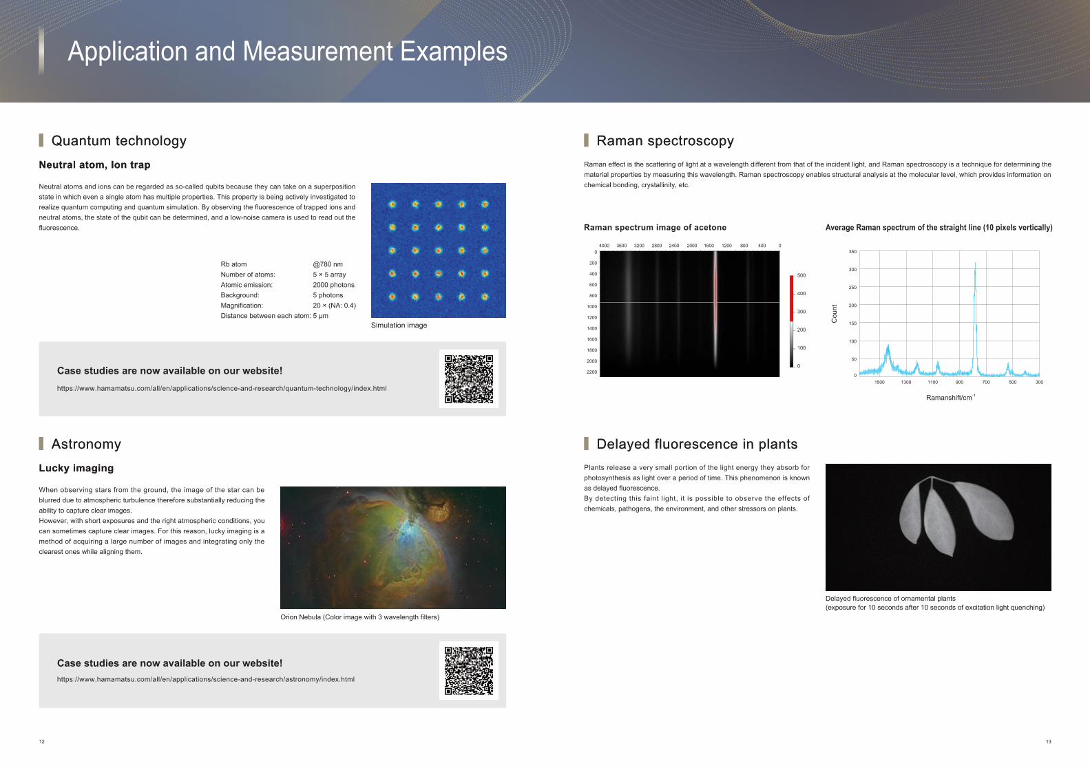
When observing stars from the ground, the image of the star can be blurred due to atmospheric turbulence therefore substantially reducing the ability to capture clear images. However, with short exposures and the right atmospheric conditions, you can sometimes capture clear images. For this reason, lucky imaging is a method of acquiring a large number of images and integrating only the clearest ones while aligning them.
Orion Nebula (Color image with 3 wavelength filters)
AstronomyAstronomyLucky imagingLucky imaging
Case studies are now available on our website!https://www.hamamatsu.com/all/en/applications/science-and-research/astronomy/index.html
Case studies are now available on our website!https://www.hamamatsu.com/all/en/applications/science-and-research/quantum-technology/index.html
Neutral atoms and ions can be regarded as so-called qubits because they can take on a superposition state in which even a single atom has multiple properties. This property is being actively investigated to realize quantum computing and quantum simulation. By observing the fluorescence of trapped ions and neutral atoms, the state of the qubit can be determined, and a low-noise camera is used to read out the fluorescence.
Quantum technologyQuantum technologyNeutral atom, Ion trapNeutral atom, Ion trap
Simulation image
Rb atom @780 nmNumber of atoms: 5 × 5 arrayAtomic emission: 2000 photonsBackground: 5 photonsMagnification: 20 × (NA: 0.4)Distance between each atom: 5 μm
Average Raman spectrum of the straight line (10 pixels vertically)
0
50
100
150
200
250
300
350
300500700900110013001500
Ramanshift/cm-1
Cou
nt
Raman spectrum image of acetone
04000 3600 3200 2800 2400 2000 1600 1200 800 400 0
200
400
600
800
1000
1200
1400
1600
1800
2000
2200
500
400
300
200
100
0
Raman effect is the scattering of light at a wavelength different from that of the incident light, and Raman spectroscopy is a technique for determining the material properties by measuring this wavelength. Raman spectroscopy enables structural analysis at the molecular level, which provides information on chemical bonding, crystallinity, etc.
Raman spectroscopyRaman spectroscopy
Delayed fluorescence of ornamental plants (exposure for 10 seconds after 10 seconds of excitation light quenching)
Plants release a very small portion of the light energy they absorb for photosynthesis as light over a period of time. This phenomenon is known as delayed fluorescence.By detecting this faint light, it is possible to observe the effects of chemicals, pathogens, the environment, and other stressors on plants.
Delayed fluorescence in plantsDelayed fluorescence in plants
12 13

Spec i f ica t ionProduct numberImaging deviceEffective number of pixelsPixel sizeEffective areaQuantum efficiency (typ.)Full well capacity (typ.)Readout noise (typ.)
Dynamic range (typ.) *1
Dark signal non-uniformity (DSNU) (typ.) *2
Photoresponse non-uniformity (PRNU) (typ.) *2*3
Linearity error
Standard scanUltra quiet scan
EMVA 1288 standard (typ.)
C15550-20UPqCMOS® image sensor4096 (H) × 2304 (V)4.6 μm (H) × 4.6 μm (V)18.841 mm (H) × 10.598 mm (V)90 % (peak QE)7000 electrons0.43 electrons rms0.27 electrons rms25 900: 10.06 electrons rms0.1 % rms0.5 %
CoolingForced-air cooled (Ambient temperature: +25 °C)Water cooled (Water temperature: +25 °C)Water cooled (max cooling) (typ.) *4
Sensor temperature−20 °C−20 °C−35 °C
Dark current (typ.)0.016 electrons/pixels/s0.016 electrons/pixels/s0.006 electrons/pixels/s
At Normal area readout and Photon number resolvingReadout modeFrame rate at full resolution
Exposure time
Trigger input
Standard scan *5
Ultra quiet scanStandard scan *5
Ultra quiet scanExternal trigger input modeSoftware triggerTrigger delay function
External trigger input modeSoftware triggerTrigger delay function
Pulse modePulse intervalBurst count
At Lightsheet readout *7
Readout modeRow interval timeExposure timeTrigger input
Full resolution, Sub-array7.2 μs to 237.6 μs7.2 μs to 271.872 msEdge / StartEdge / Start0 s to 10 s in 1 μs steps
Full resolution, Digital binning (2×2, 4×4), Sub-array120 frames/s (CoaXPress), 17.6 frames/s (USB)5 frames/s (CoaXPress, USB)7.2 μs to 1800 s199.9 ms to 1800 s *6
Edge / Global reset edge / Level / Global reset level / Sync readout / StartEdge / Global reset edge / Start0 s to 10 s in 1 μs steps
Trigger output
Master pulse
Digital outputImage processing functionInterfaceTrigger input connectorTrigger output connectorLens mountPower supplyPower consumptionAmbient operating temperatureAmbient operating humidityAmbient storage temperatureAmbient storage humidity
Global exposure timing output / Any-row exposure timing output / Trigger ready output /3 programmable timing outputs / High output / Low output
Free running / Start trigger / Burst5 μs to 10 s in 1 μs step1 to 65 53516 bit / 12 bit / 8 bitDefect pixel correction (ON or OFF, hot pixel correction 3 steps)USB 3.1 Gen 1, CoaXPress (Quad CXP-6)SMASMAC-mountAC100 V to AC240 V, 50 Hz/60 HzApprox. 155 VA0 °C to +40 °C30 % to 80 % (With no condensation)−10 °C to +50 °C90 % Max. (With no condensation)
*1: Calculated from the ratio of the full well capacity and the readout noise in Ultra quiet scan*2: In Ultra quiet scan*3: At 3500 electrons, the center 1500 × 1500 area of the image sensor, 1000 times integration*4: The water temperature is +20 ˚C and the ambient temperature is +20 ˚C*5: Normal area readout mode only*6: When global reset edge or global reset level trigger is selected, the exposure time is 172.8 µs to 1800 s. When sync readout trigger is selected, 200.2 ms to 1800 s.*7: Software such as HCImage is required. For details, please contact your local Hamamatsu representative or distributor.
14

System ConfigurationSystem Configuration
ORCA®-Quest
C-mount lens
Microscope
software
Water circulator
M9982-30 Frame grabber board CoaXPress 4BNCA14590-05-40 CoaXPress cable DIN-BNC 5 m Set of 4 (with CoaXPress)
C-mountTV adapter
StandardOption
AC adapter M9982-25Frame grabber board
with USB 3.0 A-B 3 m Cable(with USB)
PC
Dimensional OutlinesDimensional Outlines (Unit: mm)
141.6 10
4.5
18.3 113.632 50
5737 40
405070
4×ϕ4.5 ϕ8 4.53×M6×84×M3×8
1/4-20UNC×8
11055
55 110
8
55
55
4×M4×5
1-32UN×5 C-MOUNT
Camera (Approx. 3.8 kg)
OptionOptionProduct number Product nameM9982-30A14590-05-40M9982-25A12106-05A12107-05
Frame grabber board CoaXPress 4BNCCoaXPress cable DIN-BNC 5 m Set of 4Frame grabber board with USB 3.0 A-B 3 m CableExternal trigger cable SMA-BNC 5 mExternal trigger cable SMA-SMA 5 m
15

HAMAMATSU PHOTONICS K.K.Systems Division812 Joko-cho, Higashi-ku, Hamamatsu City, 431-3196, Japan, Telephone: (81)53-431-0124, Fax: (81)53-433-8031, E-mail: [email protected].: Hamamatsu Corporation: 360 Foothill Road, Bridgewater, NJ 08807, U.S.A., Telephone: (1)908-231-0960, Fax: (1)908-231-1218 E-mail: [email protected]: Hamamatsu Photonics Deutschland GmbH.: Arzbergerstr. 10, 82211 Herrsching am Ammersee, Germany, Telephone: (49)8152-375-0, Fax: (49)8152-265-8 E-mail: [email protected]: Hamamatsu Photonics France S.A.R.L.: 19, Rue du Saule Trapu, Parc du Moulin de Massy, 91882 Massy Cedex, France, Telephone: (33)1 69 53 71 00, Fax: (33)1 69 53 71 10 E-mail: [email protected] Kingdom: Hamamatsu Photonics UK Limited: 2 Howard Court,10 Tewin Road, Welwyn Garden City, Hertfordshire AL7 1BW, UK, Telephone: (44)1707-294888, Fax: (44)1707-325777 E-mail: [email protected] Europe: Hamamatsu Photonics Norden AB: Torshamnsgatan 35 16440 Kista, Sweden, Telephone: (46)8-509 031 00, Fax: (46)8-509 031 01 E-mail: [email protected]: Hamamatsu Photonics Italia S.r.l.: Strada della Moia, 1 int. 6, 20044 Arese (Milano), Italy, Telephone: (39)02-93 58 17 33, Fax: (39)02-93 58 17 41 E-mail: [email protected]: Hamamatsu Photonics (China) Co., Ltd.: 1201 Tower B, Jiaming Center, 27 Dongsanhuan Beilu, Chaoyang District, 100020 Beijing, P.R. China, Telephone: (86)10-6586-6006, Fax: (86)10-6586-2866 E-mail: [email protected]: Hamamatsu Photonics Taiwan Co., Ltd.: 8F-3, No.158, Section 2, Gongdao 5th Road, East District, Hsinchu, 300, Taiwan R.O.C. Telephone: (886)3-659-0080, Fax: (886)3-659-0081 E-mail: [email protected]
www.hamamatsu.com
Cat. No. SCAS0151E03SEP/2021 HPKCreated in Japan
● Subject to local technical requirements and regulations, availability of products included in this promotional material may vary. Please consult your local sales representative.● Information furnished by HAMAMATSU is believed to be reliable. However, no responsibility is assumed for possible inaccuracies or omissions.● Specifications and external appearance are subject to change without notice.© 2021 Hamamatsu Photonics K.K.
ORCA is registered trademark of Hamamatsu Photonics K.K. (China, France, Germany, Japan, U.K., U.S.A.)qCMOS is registered trademark of Hamamatsu Photonics K.K. (China, EU, Japan, U.K.)Product and software package names noted in this documentation are trademarks or registered trademarks of their respective manufacturers.


![[Papercraft] Orca](https://img.dokumen.tips/doc/110x75/552887e04a7959d8448b4789/papercraft-orca.jpg)