Embed Size (px)
Citation preview

Optoelectronic Control of a MMIC VCO at Ku Band
J.M. ZAMANILLO1, J. PORTILLA2, C. NAVARRO3 AND C .PÉREZ-VEGA1 1Telecommunications Engineering Department
University of Cantabria ETSII y Telecomunicación - Av. de los Castros s/n
2 Electricity and Electronic Department University of the Basque Country
3 Telefónica Sistemas Company SPAIN
http://www.unican.es
Abstract: - This paper shows the latest results research on the optical control of a GaAs chip monolithic Voltage Controlled Oscillator, and is an extension of previous work realized by our group in the field of optical-microwave interaction [1-3]. The oscillator was originally designed for the transmitter stage of a VSAT communications front-end system in the 14.5 GHz band. The possibilities of optical control of the VCO by illumination of the PHEMT transistor are demonstrated through measurements of the oscillation output power and frequency. An optical control range of 8dB of oscillation output power and up to 400MHz of oscillation frequency has been obtained. Key-Words: - OMMIC, MMIC, MESFET, P-HEMT, laser, optical power, optical-microwave interaction. 1 Introduction Along the last decade, the interest of the scientific community in the development of microwave opto-electronic systems has been increasingly stimulated because of the saturation of the microwave spectrum, and the ability to integrate microwave and optical components into a single wafer, usually designed as OMMIC (Optical Microwave Monolithic Integrated Circuit).
AlGaAs PHEMTS and GaAs MESFET devices are commonly active devices used in microwave circuit design, and many researchers, including our group, have developed accurate FET models which include optical effects [1], [2]. As a continuation of our previous works about optical controlled microwave MMIC amplifiers [3], our group has taken interest on the electro-optical control of microwave oscillators, in particular in the MMIC VCO presented in this paper. This VCO has been manufactured with the D02AH technology from the OMMIC foundry (formerly Philips-Limeil), and it is based on an AlGaAs pseudomorphic HEMT (P-HEMT) transistor with a 0.2µm gate width. It is well known that when a AlGaAs PHEMT is illuminated by a laser at a fixed wavelength, absorption effects take place at the gate-drain and gate-source inter-electrode spaces, and free carrier photo-excitation is induced at the active area level. In fact, AlGaAs P-HEMTs, as GaAs MESFETs both exhibe photoconductive and photovoltaic effects as have been previously reported [4], [5]. This means that the static DC curves, as well as the small signal
equivalent circuit parameters, change when optical energy is absorbed by the device.
The use of this GaAs technology is clear if a comparison with silicon technologies is made: GaAs has a lower noise figure, faster speed and lower DC consumption. On the other hand, GaAs technology is more expensive than that of silicon. However, the actual tendency of the market is reducing this obstacle.
A detailed description of the measurement setup is given in [1]. Here we only offer a brief explanation of this set-up. The optical source is a laser diode (λ=830 nm), pigtailed to a single-mode optical fiber (5/125). The fiber is supported by an in-house fiber holder. From the optical fiber parameters, conditions are obtained for the far field Gaussian profile [1]. The Gaussian beam diameter at the fiber end is Wo=3.1 mm and the diffraction angle is ϕ=0.085 rad. The optical energy distribution over the MESFET surface is not uniform, but we can take like effective region that where the 90% of the energy density is concentrated, as is shown in Fig.1.
The microphotograph, of the oscillator is shown in figure 2 (a) and its equivalent electrical diagram in figure 2 (b). The voltage controlled oscillator designed here, consists of an AlGaAs PHEMT transistor with 6 fingers, and 50µm of gate width. To get the appropriate frequency, the electrical control of the VCO has been implemented by the varying the bias of a varactor diode. This variable voltage capacitor has been designed using Schottky junction of another P-HEMT transistor with 4 fingers and
Proceedings of the 5th WSEAS Int. Conf. on Electronics, Hardware, Wireless and Optical Communications, Madrid, Spain, February 15-17, 2006 (pp138-141)

30µm of gate width that uses the same technology, and it is connected to the source terminal of the 6 finger device. This interconnection allows the oscillator to get a wide bandwidth (600 MHz) with a reasonable phase-noise (-85 dBc/Hz at 100 KHz). In order to avoid possible inductive mismatches that could affect the output frequency stability, due to the bonding process used in the bias wire, the gate biasing at the gate of the main transistor (6 finger device) has been avoided [6]. The output network consists only of a hairspring induction and a MIM
capacitor. The drain biasing is made through a hairspring inductor. This inductor, coupled to the output network, is used to modify the load circle of the transistor in order to improve the frequency tuning of the VCO. Furthermore, it can be appreciated in the microphotograph the necessary contact pads to place the output coplanar test probes (RFOUT), as well as DC biasing, including the varactor device. This allows the device characterization directly with a coplanar probe station, model Cascade SUMMIT 9000 coupled to a Vectorial Network Analyzer model HP8510C. The final size of the oscillator including the pads is 1200 by 750 microns. 2 Optical Control of MMICs Even when this oscillator was not designed for optical applications, it has enough optical coupling efficiency to observe this kind of interaction. In order to establish the accurate FET optical operation, preliminary experiments on the DC and pulsed I-V
Far field Gaussian profile
ϕ
roW
Wo
Single-modeOptical Fiber
z
θ
zG DS
BeamGaussian
Semi-insulating GaAs
Active layer n-GaAs-
DUTProbe Station
PigtailedLaser Diode
VNABias tee
Bias tee
VDD
Pulsed I/VSystem
Control
AA
VGGIn-house PulsedBench TR-105
HP8510 VNA
PC ControllerCurrent
& Temperature
ControlPigtailed Laser Diode
Optical Fiber
Experimental SET-UP
⎟⎟⎠
⎞⎜⎜⎝
⎛=
zorθ atan
oWπzλ.or ⋅⋅
⋅≈ 230
Ku Band MMIC VCO
Far field Gaussian profile
ϕ
roW
Wo
Single-modeOptical Fiber
z
θ
zG DS
BeamGaussian
Semi-insulating GaAs
Active layer n-GaAs-
DUTProbe Station
PigtailedLaser Diode
VNABias tee
Bias tee
VDD
Pulsed I/VSystem
Control
AA
VGGIn-house PulsedBench TR-105
HP8510 VNA
PC ControllerCurrent
& Temperature
ControlPigtailed Laser Diode
Optical Fiber
Experimental SET-UP
⎟⎟⎠
⎞⎜⎜⎝
⎛=
zorθ atan ⎟⎟⎠
⎞⎜⎜⎝
⎛=
zorθ atan
oWπzλ.or ⋅⋅
⋅≈ 230oWπzλ.or ⋅⋅
⋅≈ 230
Ku Band MMIC VCO
Fig. 1. Optical measurement set-up.
P-HEMT
S
C
VD
L
C
RFOUTC
VS L
C
LRF
LRF
VVaractor C
R
Varactor
R
CV
Fig. 2. (a) Microphotograph of the MMIC VCO.
(b) Electric scheme of the AlGaAs P-HEMT VCO.
Fig. 3. Different load cycles of the MMIC amplifier for different drain voltages of the P-HEMTdevice.
(b)
(a)
GND
GND
GND
GND
RFIN
RFOUT
Proceedings of the 5th WSEAS Int. Conf. on Electronics, Hardware, Wireless and Optical Communications, Madrid, Spain, February 15-17, 2006 (pp138-141)
characteristics curves, along with S-parameter measurements under different optical powers, were performed for the transistor alone, but not for the complete voltage controlled oscillator [4-5].
When the laser spot is properly positioned over the transistor, and the bias point selected, measurements of the amplifier scattering parameters in the band of interest (2-4 GHz) can be performed, as well as some of its main electrical characteristics, for example, input-output matching and small signal gain, can be evaluated as a function of the incident optical power on the transistor. A detailed description of the measurement setup was previously reported [1], [2]. Furthermore, on wafer measurements under no illumination (dark) conditions were previously reported [6] and a phase noise of -85 dBc/Hz at 100 KHz, was measured. Figure 3 shows simulated load cycles for the main transistor for different drain voltages. If the bias voltage VDRAIN is decreased, the
amplitude of the load cycle decreases, and as consequence of this a lower output RF power. But this effect is not very important in this case because the good match of the load cycles have been take into account during the design of the voltage controlled oscillator.
As it could be expected from theory, the effect of the optical illumination on the main PHEMT transistor of the VCO decreases the value of the oscillation frequency, due to, the increment of the gate to source capacitance of the FET. When the laser spot is properly positioned over the main transistor, (not over the PHEMT used as a varactor), and the bias point is properly selected, as well as some of its main electrical characteristics, for example, output power and oscillation frequency, can be evaluated as a function of the incident optical power on the transistor.
Figure 4 (a) shows the variation of VCO output
0 2 4 6 8 10 12-6
-5
-4
-3
-2
-1
0
1
2
3
4
PL [mW]
RF
Out
put P
ower
[dB
m]
Vd = 1.8 [V] Vs = 0 [V] -o- Vvar = 0 [V] ->- Vvar = -0.6 [V]
0 2 4 6 8 10 12-6
-5
-4
-3
-2
-1
0
1
2
3
4
PL [mW]
RF
Out
put P
ower
[dB
m]
Vd = 1.8 [V] Vs = 0 [V] -o- Vvar = 0 [V] ->- Vvar = -0.6 [V]
-0.8 -0.6 -0.4 -0.2 0 0.2 0.4 0.6 0.80
2.5
5
7.5
10
12.5
15
Varactor Voltage [V]
RF
Out
put P
ower
[dB
m]
Vs = 0 [V] Vd = 3 [V] PL = 0 [mW]
-0.8 -0.6 -0.4 -0.2 0 0.2 0.4 0.6 0.80
2.5
5
7.5
10
12.5
15
Varactor Voltage [V]
RF
Out
put P
ower
[dB
m]
Vs = 0 [V] Vd = 3 [V] PL = 0 [mW]
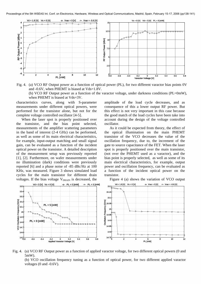
Fig. 4. (a) VCO RF Output power as a function of optical power (PL), for two different varactor bias points 0V and -0.6V, when PHEMT is biased at Vds=1.8V. (b) VCO RF Output power as a function of the varactor voltage, under darkness conditions (PL=0mW), when PHEMT is biased at Vds=3V.
-0.8 -0.6 -0.4 -0.2 0 0.2 0.4 0.6 0.814.5
14.6
14.7
14.8
14.9
15
15.1
15.2
15.3
15.4
15.5
Applied Varactor Voltage [V]
VC
O O
scill
atio
nFr
eque
ncy
[GH
z]
Vd = 3 [V] Vs = 0 [V] -o- PL = 0 [mW] ->- PL = 5 [mW]
PL = 0 [mW]
PL = 5 [mW]
-0.8 -0.6 -0.4 -0.2 0 0.2 0.4 0.6 0.814.5
14.6
14.7
14.8
14.9
15
15.1
15.2
15.3
15.4
15.5
Applied Varactor Voltage [V]
VC
O O
scill
atio
nFr
eque
ncy
[GH
z]
Vd = 3 [V] Vs = 0 [V] -o- PL = 0 [mW] ->- PL = 5 [mW]
PL = 0 [mW]
PL = 5 [mW]
0 2 4 6 8 10 12
14.75
14.8
14.85
14.9
14.95
15
15.05
15.1
15.15
15.2
PL [mW]
Osc
illat
ion
Freq
uenc
y[G
Hz]
Vd = 1.8 [V] Vs = 0 [V] -o- Vvar = 0 [V] ->- Vvar = -0.6 [V]
0 2 4 6 8 10 1214.75
14.8
14.85
14.9
14.95
15
15.05
15.1
15.15
15.2
PL [mW]
Osc
illat
ion
Freq
uenc
y[G
Hz]
Vd = 1.8 [V] Vs = 0 [V] -o- Vvar = 0 [V] ->- Vvar = -0.6 [V]
Fig. 4. (a) VCO RF Output power as a function of applied varactor voltage, for two different optical powers (0 and 5mW). (b) VCO oscillation frequency tuning as a function of optical power, for two different applied varactor voltages (0 and -0.6V).
Proceedings of the 5th WSEAS Int. Conf. on Electronics, Hardware, Wireless and Optical Communications, Madrid, Spain, February 15-17, 2006 (pp138-141)

power as a function of the optical power applied for two different varactor voltages, (0 and -0.6 V), keeping the drain voltage constant at 1.8V in both traces. When varactor voltage is fixed to 0V (Vvar=0V), the output power of the VCO is independent with the optical illumination, due to that, in this region of work the output power is independent of the circuit capacitance and this capacitance depends strongly on the optical power [5]. The origin of this it could be extracted from figure 4 (b), in this figure, it could be appreciated how from a certain varactor voltage (-0.3 V in our MMIC), the oscillator generates the maximum RF output power available, below this bias point the effect of the optical illumination is more important, as shown in fig 4 (a) for the trace Vvar=-0.6V.
Figure 4 (a) shows the variation of the VCO oscillation frequency as a function of the varactor voltage for two different optical powers of 0 and 5mW, keeping constant the drain voltage at 3V. The optical tuning range for the VCO studied here under the above mentioned optical powers, varies up to 400 MHz as is shown in figure 4 (a) for Vvar=-0,7V. On the other hand, the tuning optical range for this VCO, varies only 200 MHz when increasing the varactor biasing (Vvar=0V and Vvar=-0.6V), as is shown in figure 4 (b). 3 Conclusion An exhaustive investigation of the control properties of a GaAs MMIC VCO at Ku band under optical illumination has been performed.
The main dependencies of its parameters, as well as the way of integrating their behavior into other classical controlling techniques for the drain and gate currents has been shown. The optical control procedure presented here is also valid for other types of microwave components and subsystems such as amplifiers, mixers, up-converters, down-converters, etc. [8] and this technique may improve the development of future generations of OMMICS.
As a conclusion of the work presented here, it can be established that the CW laser optical control gives the user another port to modify the characteristics of the microwave device, the oscillation frequency and output power for the VCO. In that sense the acronyms OVCO (Optical and Voltage Controlled Oscillator) must be used in the future to refer to this kind of devices. Acknowledgment This work has been partially supported by the Spanish Ministerio de Educación y Ciencia through the project TEC2005-07985-C03-01.
Furthermore, authors would to thank the project NoE TARGET (IST program of the EU under contract IST-1-707893-NOE) the facilities for the realization of the present work. References: [1] J.M. Zamanillo, C. Navarro, C. Pérez-Vega, A.
Mediavilla, and A. Tazón Large Signal Model Predicts Dynamic Behavior of GaAs MESFET Under Optical Illumination.. Microwave and Optical Technology Letters. Vol. 29, No.1, pp 25-31. April 5 2001.
[2] C. Navarro, J.M. Zamanillo, A. Mediavilla, A. Tazón and J.L. García, New optical capacitance Model for GaAs MESFETs. Microwave and Optical Technology Letters, Vol. 26, No. 1, pp. 16-21. Jul 2000
[3] J.M. Zamanillo, J. Portilla, C. Navarro, C. Pérez-Vega and A. Mediavilla, Optical Control of a GaAs MMIC Amplifier at S Band. GaAs 2003 European Gallium Arsenide, Applications Symposium Proceedings, pp.117-120, Munich, Germany. Oct. 2003
[4] C. Navarro, A. Mediavilla, A. Tazón, J.M. Zamanillo, J.L. García, M. Lomer and J.M. López-Higuera. An Accurate Photonic Capacitance Model for GaAs MESFET”, IEEE Transactions on MTT, Vol 50, No. 4, pp 1193-1197, April 2002.
[5] J. M. Zamanillo, C. Navarro, C. Pérez-Vega, J. A. García, A. Mediavilla and A. Tazón. New Large Signal Model of AlGaAs P-HEMT and GaAs MESFET Under Optical Illumination. GaAs 2002 European Gallium Arsenide, Applications Symposium Proceedings, pp.121-124.Milan, Italy. Sept. 2002.
[6] J. Portilla, J. P. Pascual, Mª. L. de la Fuente, E. Artal, MMIC VCO Design Approaches for Low Noise and Enhanced Power Performances, European Microwave Conference EuMC, Amsterdam 1998.
[7] J.M. Zamanillo, C. Navarro, J. Sáiz-Ipiña, C. Pérez-Vega and A. Mediavilla. New Large Signal Electrical Model of GaAs MESFET Under Optical Illumination. GaAs 2001 European Gallium Arsenide, Applications Symposium Proceedings, pp.167-170, London , Sept-2001.
[8] J.M. Zamanillo, J. Portilla, C. Navarro and C. Pérez-Vega. Optical Ports: Next generation of MMIC control devices?, 35th European Microwave Conference (EuMC), Paris Oct. 2005, pp. 1391- 1394, CD-ROM Proceedings. ISBN 2-9600551-0-1.
Proceedings of the 5th WSEAS Int. Conf. on Electronics, Hardware, Wireless and Optical Communications, Madrid, Spain, February 15-17, 2006 (pp138-141)