Embed Size (px)
Citation preview

OOVA & OTAVA & OTA##33
1Radivoje Đurić, 2015, Analogna Integrisana Kola

Three-stage amplifier•In many applications, operational amplifiers are required which have three stages. ForIn many applications, operational amplifiers are required which have three stages. Forexample, class AB amplifiers have an output stage which provide little gain but a lot of current.The first two stages are now needed to provide gain.•Also, when the supply voltage is less than 1V, more stages are required as cascoding is nol ibllonger possible.•With three stages, stability is less obvious than two stages•Cascoding or cascading?
Radivoje Đurić, 2015, Analogna Integrisana Kola2
High voltage, low power Low-voltage, high power

•A single-stage amplifier has only one single highimpedance point at the output. The outputcapacitance CL determines the GBW.I th f i bl l d it i it h d it filt d t t th•In the case of variable load capacitances, as in switched-capacitor filters, we do not want the
GBW to depend on the load. A two-stage opamp is then better used.•A two-stage amplifier has two high-impedance points. They need to be connected by acompensation capacitance Cc to provide pole splitting and to generate a dominant pole. Thecompensation capacitance Cc to provide pole splitting and to generate a dominant pole. TheGBW is therefore determined by this compensation capacitance Cc.
For stability, the nondominant pole is nowd t i d b th l d it CL It t bdetermined by the load capacitance CL. It must besufficiently large compared to the GBW, to providea sufficient phase margin. A ratio of three is takenfor a phase margin of about 70°.p g
Since three high-impedance points are present,two compensation capacitances are required forstability. Both are connected to the output. This iscalled nested-Miller compensation.
Radivoje Đurić, 2015, Analogna Integrisana Kola3

•As a result, we find two non-dominant poles. Both have to be positioned sufficiently farbeyond the GBW, such that together they provide a reasonable phase margin.3-pole op amp : phase margin PM
•Ratio’s of 2 5 and 7 would also be acceptable but positioning a non-dominant pole at 7 timesRatio s of 2.5 and 7 would also be acceptable but positioning a non dominant pole at 7 timesthe GBW would probably require too much power. This combination is better avoided.•It is also clear that a PM of about 60° is sufficiently high, even if a bit of peaking occurs. A PMof 70° would require non-dominant poles at too high frequencies, and would consume toomuch power.•Many designers take an even higher risk by requiring a PM of only 50°. In this case, thetransient response is really on the edge of peaking. The non-dominant poles can then bepositioned at 2 and 4 times the GBW only! This is called the Butterworth response It provides
Radivoje Đurić, 2015, Analogna Integrisana Kola4
positioned at 2 and 4 times the GBW only! This is called the Butterworth response. It providesa maximally flat response once the feedback loop is closed towards unity gain.

Open loop gain:
Closed loop gain (Unity gain):
Three-stage with 3/5 on 600 PM Three-stage with 3/5 on 600 PM
Nested-Miller Frequency compensation – NMCNested-Miller Frequency compensation – NMC
It cannot be used as a second-stage of aIt cannot be used as a second stage of athreestage amplifier. Otherwise compensationcapacitance Cc1 would provide positivefeedback!
Radivoje Đurić, 2015, Analogna Integrisana Kola5

•In an open loop, three poles occur and twozeros.
•The dominant pole is caused by the Miller effect of the overall compensation capacitanceCm1 1
d C R R R
•The GBW is determined by this capacitance Cm1 and the input transconductance1m
UGgC
1 2 3 1 2 3d
m m mC g g R R R
•We can normally assume that the transconductances increase towards the output•For a 3rd-order Butterworth response, the two non-dominant poles p1 and p2 have to be putat 2 and 4 times the GBW, ω2 = 2 ωUG. ω1 = 4 ωUG. Both zeros are usually negligible.
1UG
mC
at 2 and 4 times the GBW, ω2 2 ωUG. ω1 4 ωUG. Both zeros are usually negligible.•Note that we still have to solve a system of three equations (for the GBW, ω1 and ω2) andfive variables.•Normally, the two compensation capacitances are chosen. The first one Cm1 can be chosen
ll ibl i t l t th ti th d it t th t t f th fi t
Radivoje Đurić, 2015, Analogna Integrisana Kola6
as small as possible, i.e. at least three times the node capacitance at the output of the firststage but not so small that the input noise is too high.

•The other capacitance Cm2 can also be chosen as small as possible, i.e. at least three timesthe node capacitance at the output of the second stage.Mi i l f th ti it l h t d th•Minimum values of these compensation capacitances are always chosen to reduce the
power consumption as much as possible•Of course, if noise is an important specification, then these capacitances may have to beincreased, increasing the power consumption. As expected, low noise always leads to largerincreased, increasing the power consumption. As expected, low noise always leads to largerpower consumption.
Nested Gm-C compensation NGCC
•This three-stage configuration has nested Millercompensation with additional Gm blocks forcompensation with additional Gm blocks forrealizing two feedforward paths. If theirtransconductances are chosen to be the sameas their corresponding stage transconductancesthen both zeros’ are cancelled out.•The two resulting nondominant poles are thenthe same as for a conventional NMC amplifier.
g g21
2
m
m
gC
32
m
L
gC
Radivoje Đurić, 2015, Analogna Integrisana Kola7
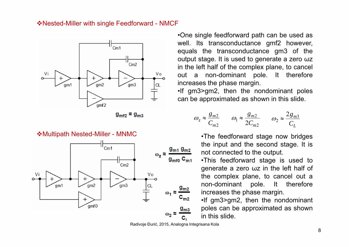
Nested-Miller with single Feedforward - NMCF
•One single feedforward path can be used aswell. Its transconductance gmf2 however,equals the transconductance gm3 of theoutput stage. It is used to generate a zero ωzin the left half of the complex plane to cancelin the left half of the complex plane, to cancelout a non-dominant pole. It thereforeincreases the phase margin.•If gm3>gm2, then the nondominant polescan be approximated as shown in this slide.
2
2
mz
gC
21
22mg
C 3
22 mgC
Multipath Nested-Miller - MNMC •The feedforward stage now bridgesthe input and the second stage. It isnot connected to the output
2mC 22 mC LC
not connected to the output.•This feedforward stage is used togenerate a zero ωz in the left half ofthe complex plane, to cancel out ap pnon-dominant pole. It thereforeincreases the phase margin.•If gm3>gm2, then the nondominantpoles can be approximated as shown
Radivoje Đurić, 2015, Analogna Integrisana Kola8
poles can be approximated as shownin this slide.

Comparison Nested-Miller solutions•For sake of comparison all previous amplifiers are listed in a table. They are preceded by ai l t d t t Mill lifisingle-stage and a two-stage Miller amplifier.
•All of them have a comparable phase margin except for the single-stage amplifier. Theresulting GBW for a 3rd-order Butterworth design is also listed as a fraction of the output timeconstant gm3/CL.constant gm3/CL.•The next column shows what GBW can be expected, compared to a single-stage amplifier.The conventional NMC amplifier only achieves about ¼ of what a single stage can achieve.•When compared to a NMC amplifier (in the last column), it is clear that both last amplifiers
hi h i l f df d t d b tt i t f ti H thwhich use a single feedforward stage do better in terms of power consumption. However, theimprovement is at best a factor of 2.
Radivoje Đurić, 2015, Analogna Integrisana Kola9

Three-stage op amp•The first stage is implemented by the differential input transistors, T1−T2, biased by T15, andloaded by T3−T8 while the second and third ones consist of T9 −T12 and T13 respectivelyloaded by T3 T8, while the second and third ones consist of T9 T12 and T13, respectively.The compensation capacitors Cc1 and Cc2 are used to stabilize the amplifier.•The first and third gain stages are of the inverting type. The noninverting second amplification section is required to ensure the negative feedback around the nested compensation paths.
Radivoje Đurić, 2015, Analogna Integrisana Kola10

•The node capacitances are given by:
•The zero frequencies are usually much greater than the unity-gain frequency of the amplifier.
Radivoje Đurić, 2015, Analogna Integrisana Kola11
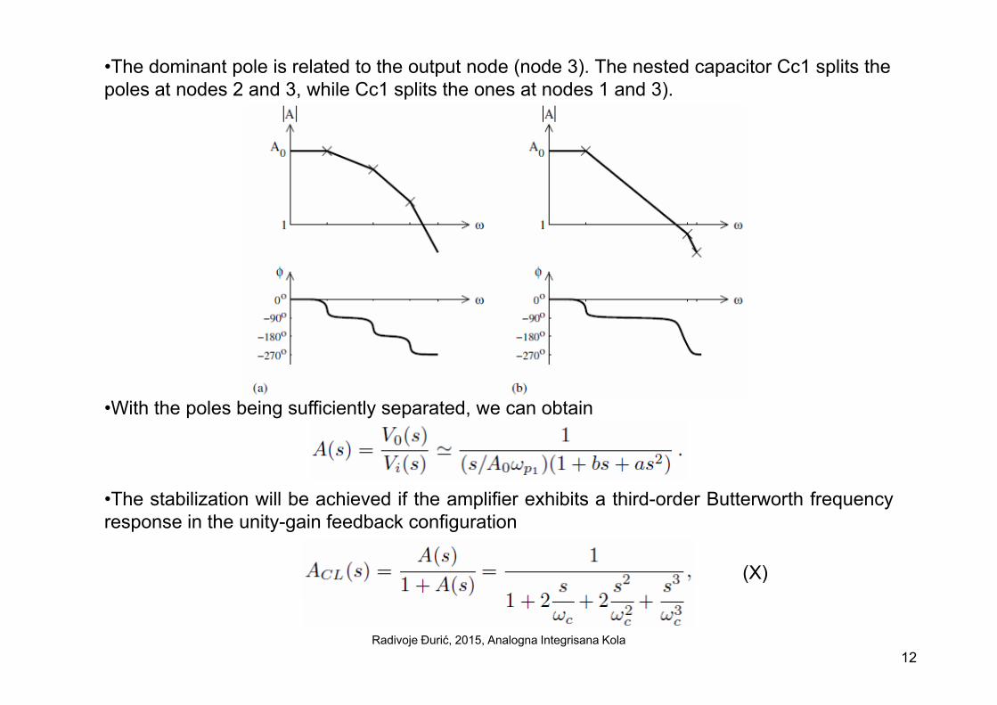
•The dominant pole is related to the output node (node 3). The nested capacitor Cc1 splits the poles at nodes 2 and 3, while Cc1 splits the ones at nodes 1 and 3).
•With the poles being sufficiently separated, we can obtain
•The stabilization will be achieved if the amplifier exhibits a third-order Butterworth frequencyresponse in the unity-gain feedback configuration
(X)
Radivoje Đurić, 2015, Analogna Integrisana Kola12

where ωc is the cutoff frequency
(Y)
•Comparing Equations (X) and (Y) gives
This leads to the values of the compensation capacitors given by
•Because the Butterworth response is said to be under-damped, it can also yield the minimump p , ysettling time. It is characterized by a unity-gain phase margin given by
•With A0ωp1 and ωc representing the amplifier unity-gain frequency and the cutoff frequency
Radivoje Đurić, 2015, Analogna Integrisana Kola13
p p g p y g q y q yof the Butterworth response, respectively, it was assumed that A0ωp1/ωc = 1/2.

•Note that the locations of the nondominant poles depend on C3 and the amplifier stability canbe affected by the output load capacitor. The gainbandwidth product is given by
•The resulting GBW is four times smaller than the one of an uncompensated structure. TheThe resulting GBW is four times smaller than the one of an uncompensated structure. Theslew rate (SR) of the amplifier can be obtained as
where IB1, IB2, and IB3 are the bias current of the first, second, and third stage, respectively.•The amplifier should exhibit a poor SR for large compensation capacitors!•Generally, an N-stage amplifier needs N − 1 compensation capacitors driven by the outputGenerally, an N stage amplifier needs N 1 compensation capacitors driven by the outputstage. In this case, the requirement of a large bandwidth can be fulfilled only at the price of ahigh-power consumption.•Due to the fact that both compensation capacitors affect the amplifier loading, the bandwidth
hi bl ith th t d Mill ti i li it d A i t b bt i dachievable with the nested Miller compensation is limited. An improvement can be obtainedusing amplifiers based on the reversed nested Miller compensation, especially when drivinglarge capacitive loads.
Radivoje Đurić, 2015, Analogna Integrisana Kola14

Three-stage reversed active feedback frequency compensation (RAFFC) amplifier
It consists of an input stage with the folded-cascode structure, a common-source invertingstage, and a noninverting output stage. The feed-forward transconductance is realized bylinking the gate of the load transistor T14 to the first stage output, while the feedbacktransconductance is obtained by connecting Cc1 to the source of T6 instead of the first stageoutput.
Radivoje Đurić, 2015, Analogna Integrisana Kola15
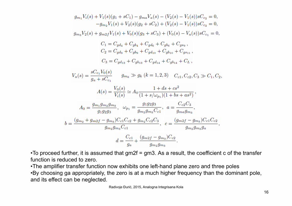
•To proceed further, it is assumed that gm2f = gm3. As a result, the coefficient c of the transferfunction is reduced to zero.•The amplifier transfer function now exhibits one left-hand plane zero and three poles•By choosing ga appropriately the zero is at a much higher frequency than the dominant pole
Radivoje Đurić, 2015, Analogna Integrisana Kola16
•By choosing ga appropriately, the zero is at a much higher frequency than the dominant pole,and its effect can be neglected.

•The stability of the amplifier can then be ensured by considering that the denominator of thetransfer function in the unity-gain closed-loop configuration is a third-order Butterworthpolynomial with a cutoff frequency of ωcpolynomial with a cutoff frequency of ωc.
•By solving the system of equations, the values of the compensation capacitors can beobtained asobtained as
•The gain-bandwidth product of the amplifier is of the form
•Because N > 1, the GBW of the RAFFC amplifier is much greater than the one of the NMCamplifier.•The phase margin of the RAFFC amplifier can be computed as
Radivoje Đurić, 2015, Analogna Integrisana Kola17

•Due to the contribution of the left-hand plane zero, the phase margin is greater than thevalue of 60o obtained in the case of the NMC amplifier.•The slew rate depends upon the value of compensation capacitors and the bias currents•The performance improvement provided by three-stage amplifiers using nestedcompensation is obtained at the expense of power dissipationcompensation is obtained at the expense of power dissipation•To overcome this limitation, the amplifier architecture shown in the next figure
Three-stage amplifier with a single RC compensation
•The start-up circuit consisting of transistors TS1 − TS3 is used to prevent the bias circuit,TB1 − TB4, from entering the zero-current state. When the circuit is powered up, the voltageVP at the gates of transistors TB3 and TB4 begins to increase while the voltage VQ at the
Radivoje Đurić, 2015, Analogna Integrisana Kola18
VP at the gates of transistors TB3 and TB4 begins to increase, while the voltage VQ at thegates of transistors TB1 and TB2 may remain at zero.

•When the circuit is powered up, the voltage VP at the gates of transistors TB3 and TB4begins to increase, while the voltage VQ at the gates of transistors TB1 and TB2 may remaintat zero.
•Because the difference voltage VP −VQ is greater than the sum of two threshold voltages,2VTn, both transistors TS2 and TS3 are conducting and the start-up current can be injected inthe bias circuits.the bias circuits.•When the normal operation state is subsequently reached, the voltage VP −VQ becomesless than 2VTn, such that at least the transistor TS3 is biased in the cutoff region. The start-upis then deactivated.C id i th bi i it it b f d th t•Considering the bias circuit, it can be found that
•The small-signal equivalent circuit of the three-stage amplifier with a single RC compensationis depicted in the next figure, where Cp1, Cp2, and Cp3 denote the parasitic couplingcapacitors
Radivoje Đurić, 2015, Analogna Integrisana Kola19
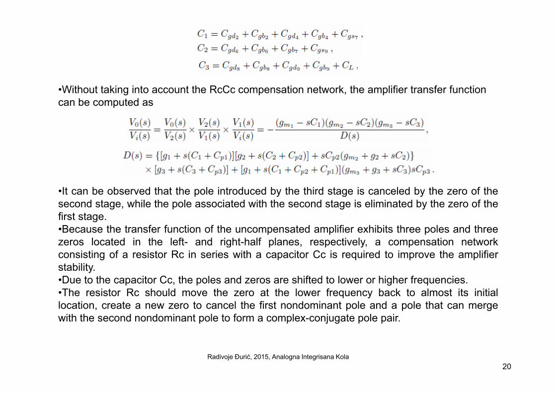
•Without taking into account the RcCc compensation network, the amplifier transfer function can be computed asp
•It can be observed that the pole introduced by the third stage is canceled by the zero of thep y g ysecond stage, while the pole associated with the second stage is eliminated by the zero of thefirst stage.•Because the transfer function of the uncompensated amplifier exhibits three poles and threezeros located in the left and right half planes respectively a compensation networkzeros located in the left- and right-half planes, respectively, a compensation networkconsisting of a resistor Rc in series with a capacitor Cc is required to improve the amplifierstability.•Due to the capacitor Cc, the poles and zeros are shifted to lower or higher frequencies.•The resistor Rc should move the zero at the lower frequency back to almost its initiallocation, create a new zero to cancel the first nondominant pole and a pole that can mergewith the second nondominant pole to form a complex-conjugate pole pair.
Radivoje Đurić, 2015, Analogna Integrisana Kola20
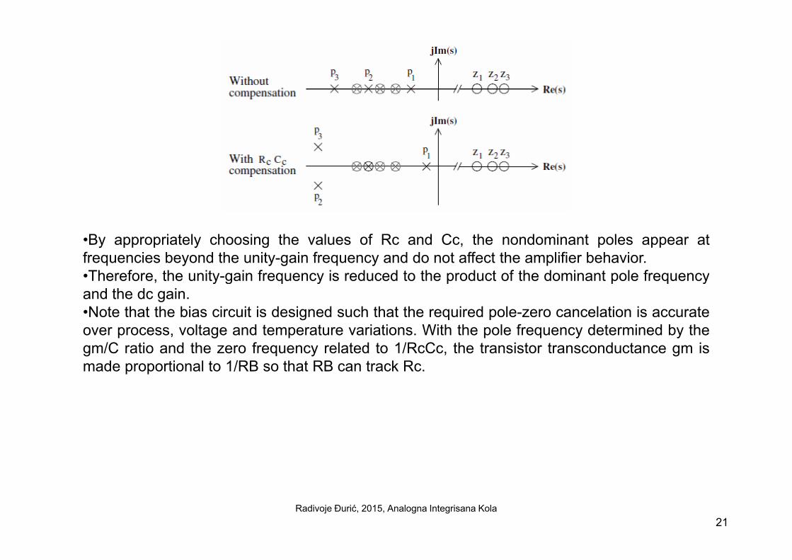
•By appropriately choosing the values of Rc and Cc, the nondominant poles appear atfrequencies beyond the unity-gain frequency and do not affect the amplifier behavior.•Therefore, the unity-gain frequency is reduced to the product of the dominant pole frequencyTherefore, the unity gain frequency is reduced to the product of the dominant pole frequencyand the dc gain.•Note that the bias circuit is designed such that the required pole-zero cancelation is accurateover process, voltage and temperature variations. With the pole frequency determined by the
/C ti d th f l t d t 1/R C th t i t t d t igm/C ratio and the zero frequency related to 1/RcCc, the transistor transconductance gm ismade proportional to 1/RB so that RB can track Rc.
Radivoje Đurić, 2015, Analogna Integrisana Kola21