Embed Size (px)
Citation preview

UNIVERSITY OF CALIFORNIA, SAN DIEGO
Nonlinear Active Metamaterial Surfaces
A Dissertation submitted in partial satisfaction of therequirements for the degree
Doctor of Philosophy
in
Electrical Engineering (Electronic Circuits and Systems)
by
Sanghoon Kim
Committee in charge:
Professor Daniel F. Sievenpiper, ChairProfessor Todd P. ColemanProfessor William S. HodgkissProfessor Boubacar KanteProfessor Vitaliy Lomakin
2017

Copyright
Sanghoon Kim, 2017
All rights reserved.

The Dissertation of Sanghoon Kim is approved, and it is
acceptable in quality and form for publication on microfilm
and electronically:
Chair
University of California, San Diego
2017
iii

DEDICATION
To my beloved wife Jung-A Chu and adorable angel Dana Kim,
and my parents Mr. Sung-Soo Kim and Mrs. Seung-Ok Jang.
iv
TABLE OF CONTENTS
Signature Page . . . . . . . . . . . . . . . . . . . . . . . . . . . . . . . . . . . . . iii
Dedication . . . . . . . . . . . . . . . . . . . . . . . . . . . . . . . . . . . . . . . . iv
Table of Contents . . . . . . . . . . . . . . . . . . . . . . . . . . . . . . . . . . . . v
List of Figures . . . . . . . . . . . . . . . . . . . . . . . . . . . . . . . . . . . . . . vii
List of Tables . . . . . . . . . . . . . . . . . . . . . . . . . . . . . . . . . . . . . . ix
List of Abbreviations . . . . . . . . . . . . . . . . . . . . . . . . . . . . . . . . . . x
Acknowledgements . . . . . . . . . . . . . . . . . . . . . . . . . . . . . . . . . . . xi
Vita . . . . . . . . . . . . . . . . . . . . . . . . . . . . . . . . . . . . . . . . . . . xiii
Abstract of the Dissertation . . . . . . . . . . . . . . . . . . . . . . . . . . . . . . . xv
Chapter 1 Introduction . . . . . . . . . . . . . . . . . . . . . . . . . . . . . . . 11.1 Motivation . . . . . . . . . . . . . . . . . . . . . . . . . . . . . 21.2 Metamaterial Surfaces . . . . . . . . . . . . . . . . . . . . . . 51.3 Dissertation Organization . . . . . . . . . . . . . . . . . . . . . 9
Chapter 2 Theoretical Limitations for TM Surface Wave Attenuation by LossyCoatings on Conducting Surfaces . . . . . . . . . . . . . . . . . . . . 112.1 Overview of TM Surface Wave Attenuation . . . . . . . . . . . 122.2 Analytical Solution . . . . . . . . . . . . . . . . . . . . . . . . 13
2.2.1 Without Impedance Sheet . . . . . . . . . . . . . . . . 132.2.2 With Impedance Sheet . . . . . . . . . . . . . . . . . . 20
2.3 Numerical Solution . . . . . . . . . . . . . . . . . . . . . . . . 242.4 Results . . . . . . . . . . . . . . . . . . . . . . . . . . . . . . 27
2.4.1 Validation of Analytical Solution . . . . . . . . . . . . . 272.4.2 Theoretical Limitations . . . . . . . . . . . . . . . . . . 28
2.5 Conclusion . . . . . . . . . . . . . . . . . . . . . . . . . . . . 33
Chapter 3 Switchable Nonlinear Metasurfaces for Absorbing High Power SurfaceWaves . . . . . . . . . . . . . . . . . . . . . . . . . . . . . . . . . . 353.1 Overview of Concept . . . . . . . . . . . . . . . . . . . . . . . 363.2 Mechanism of Switchable Metasurface . . . . . . . . . . . . . . 373.3 Measurement of Nonlinear Metasurface . . . . . . . . . . . . . 40
3.3.1 Linear Measurement in Waveguides . . . . . . . . . . . 403.3.2 Surface Wave Measurement . . . . . . . . . . . . . . . 443.3.3 Leakage Field Measurement . . . . . . . . . . . . . . . 45
v
3.4 Conclusion . . . . . . . . . . . . . . . . . . . . . . . . . . . . 54
Chapter 4 Self-Tuning Metamaterial Surfaces . . . . . . . . . . . . . . . . . . . 564.1 Concept and Mechanism . . . . . . . . . . . . . . . . . . . . . 56
4.1.1 Background and Motivation . . . . . . . . . . . . . . . 564.1.2 Mechanisms for Self-Tuning Metasurfaces . . . . . . . 58
4.2 Self-Tuning Circuit Board . . . . . . . . . . . . . . . . . . . . 614.2.1 Rectifying Diode . . . . . . . . . . . . . . . . . . . . . 624.2.2 Impedance Matching Network . . . . . . . . . . . . . . 634.2.3 DC-Pass Filter . . . . . . . . . . . . . . . . . . . . . . 64
4.3 Responding Part of Self-Tuning Metasurface . . . . . . . . . . 654.4 Measurement and Results . . . . . . . . . . . . . . . . . . . . . 654.5 Conclusion . . . . . . . . . . . . . . . . . . . . . . . . . . . . 67
Chapter 5 Reconfigurable Impedance Ground Plane . . . . . . . . . . . . . . . 695.1 Background and Motivation . . . . . . . . . . . . . . . . . . . 705.2 Simulation Results . . . . . . . . . . . . . . . . . . . . . . . . 745.3 Prototype Reconfigurable Surface . . . . . . . . . . . . . . . . 76
5.3.1 Simulation Data of Prototype Sample . . . . . . . . . . 765.3.2 RF Switch . . . . . . . . . . . . . . . . . . . . . . . . . 785.3.3 Measurement . . . . . . . . . . . . . . . . . . . . . . . 79
5.4 Conclusion . . . . . . . . . . . . . . . . . . . . . . . . . . . . 82
Chapter 6 Omni-Directional Metamaterial Surface . . . . . . . . . . . . . . . . 836.1 Background and Motivation . . . . . . . . . . . . . . . . . . . 836.2 Mechanism of Omni-Directional Metasurface . . . . . . . . . . 866.3 Simulation and Measurement of Omni-Directional
Metasurface . . . . . . . . . . . . . . . . . . . . . . . . . . . . 896.4 Conclusion . . . . . . . . . . . . . . . . . . . . . . . . . . . . 93
Chapter 7 Conclusion . . . . . . . . . . . . . . . . . . . . . . . . . . . . . . . 947.1 Summary of Work . . . . . . . . . . . . . . . . . . . . . . . . . 947.2 Future Work . . . . . . . . . . . . . . . . . . . . . . . . . . . . 95
Bibliography . . . . . . . . . . . . . . . . . . . . . . . . . . . . . . . . . . . . . . 96
vi

LIST OF FIGURES
Figure 1.1: Possible interference points on the conductive enclosure. . . . . . . . . 2Figure 1.2: Leakage fields on the conductive enclosure due to the high power waves. 3Figure 1.3: Dispersion diagram of the high impedance surface. . . . . . . . . . . . 4Figure 1.4: The index of refraction in ε - µ diagram. . . . . . . . . . . . . . . . . . 6Figure 1.5: Artificial magnetic conductor properties of the high impedance surface. 8Figure 1.6: Scheme of the high impedance surface (HIS). . . . . . . . . . . . . . . 9
Figure 2.1: Schematic of the structure and properties of materials. . . . . . . . . . 14Figure 2.2: Schematic for the numerical solutions and assigned boundaries. . . . . 25Figure 2.3: Matching plot between the analytical and numerical solutions with an
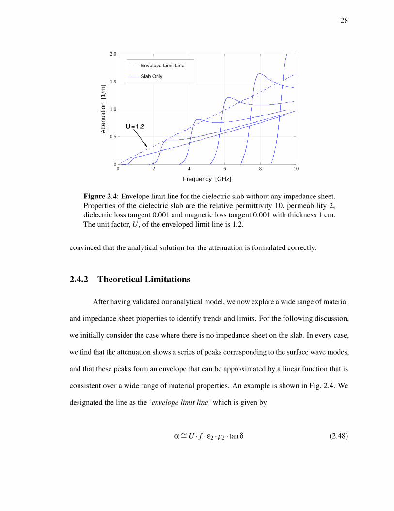
impedance sheet. . . . . . . . . . . . . . . . . . . . . . . . . . . . . . 27Figure 2.4: Envelope limit line for the dielectric slab without any impedance sheet. 28Figure 2.5: Comparison of attenuation values when adding an impedance sheet to
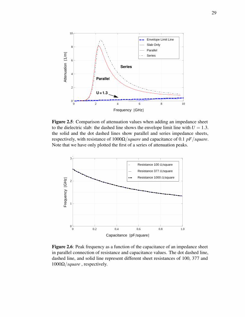
the dielectric slab. . . . . . . . . . . . . . . . . . . . . . . . . . . . . 29Figure 2.6: Peak frequency as a function of the capacitance of an impedance sheet. 29Figure 2.7: Attenuation value for different thickness of the slab with an impedance
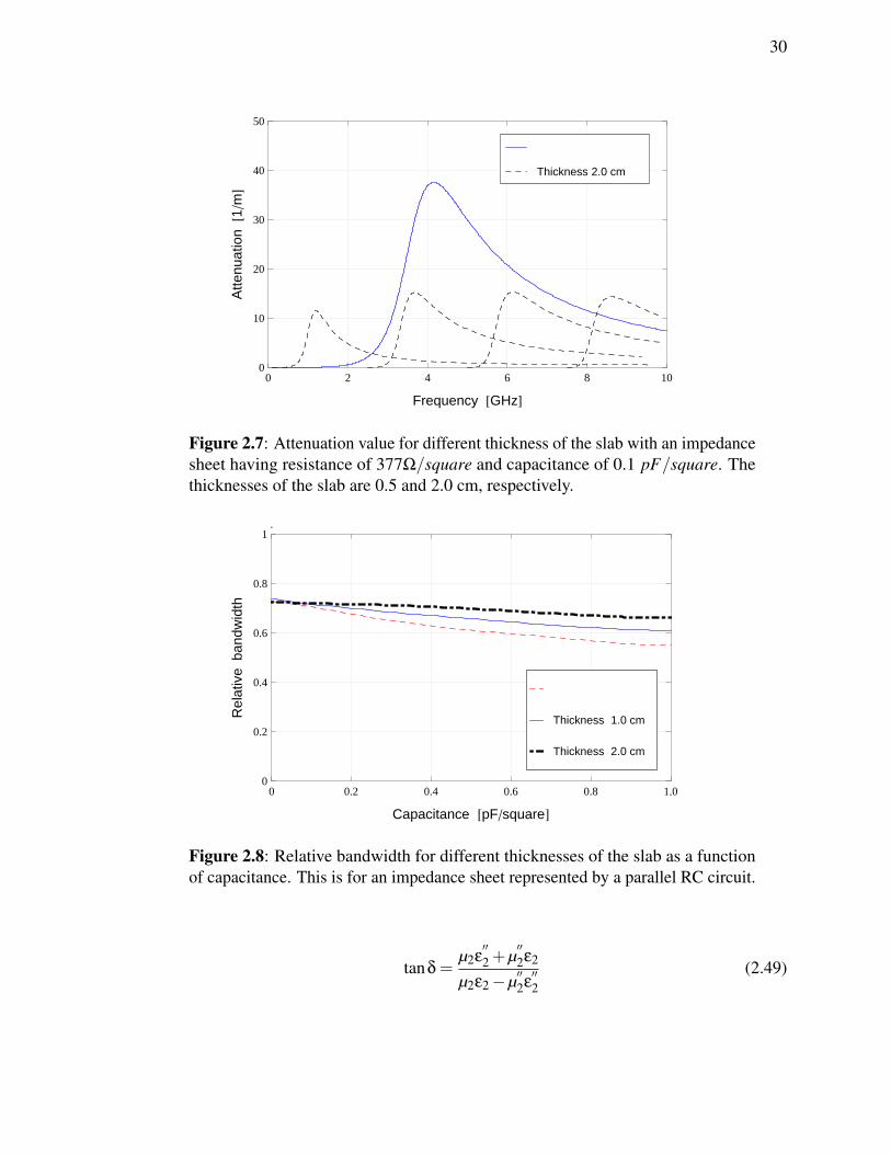
sheet. . . . . . . . . . . . . . . . . . . . . . . . . . . . . . . . . . . . 30Figure 2.8: Relative bandwidth for different thicknesses. . . . . . . . . . . . . . . 30Figure 2.9: Relative bandwidth for different slab properties. . . . . . . . . . . . . . 31Figure 2.10: Peak attenuation values as a function of resistance. . . . . . . . . . . . 31
Figure 3.1: Nonlinear metasurfaces for power dependent absorption. . . . . . . . . 38Figure 3.2: Measurement setup for linear waveguide measurement. . . . . . . . . . 40Figure 3.3: Transient simulation data of the on/off states . . . . . . . . . . . . . . 41Figure 3.4: Simulation and measurement of the nonlinear metasurface inside the
waveguides. . . . . . . . . . . . . . . . . . . . . . . . . . . . . . . . . 42Figure 3.5: Comparison of the absorbing profiles with a typical magRAM. . . . . . 43Figure 3.6: Measurement setup for surface field suppression. . . . . . . . . . . . . 44Figure 3.7: Measurement of the surface field profiles under different power levels. . 46Figure 3.8: Off-State surface field profiles of the metasurface . . . . . . . . . . . . 47Figure 3.9: On-State surface field profiles of the metasurface . . . . . . . . . . . . 48Figure 3.10: Off-State surface field profiles of the magRAM . . . . . . . . . . . . . 49Figure 3.11: On-State surface field profiles of the magRAM . . . . . . . . . . . . . 50Figure 3.12: The leakage field measurement setup and results. . . . . . . . . . . . . 52Figure 3.13: Measurement setup for leakage fields through the conductive enclosure. 53
Figure 4.1: Mechanism diagram for the self-tuning metasurface . . . . . . . . . . . 58Figure 4.2: Scheme of the co-simulation . . . . . . . . . . . . . . . . . . . . . . . 59Figure 4.3: Overall scheme of the self-tuning circuit board. . . . . . . . . . . . . . 60Figure 4.4: ADS circuit scheme for the rectifying diode . . . . . . . . . . . . . . . 62Figure 4.5: Input impedance of the rectifying diode . . . . . . . . . . . . . . . . . 62Figure 4.6: Model and simulation data of impedance matching network . . . . . . 63
vii

Figure 4.7: Model and simulation data of DC-pass filter . . . . . . . . . . . . . . . 64Figure 4.8: Fabricated sample of the self-tuning metasurface . . . . . . . . . . . . 65Figure 4.9: Scheme of the measurement setup . . . . . . . . . . . . . . . . . . . . 66Figure 4.10: A photo of the measurement setup in the anechoic chamber . . . . . . . 67Figure 4.11: Measurement data from the self-tuning metasurface . . . . . . . . . . . 68
Figure 5.1: A diagram and mechanism of the reconfigurable impedance ground plane. 71Figure 5.2: A scheme of the reconfigurable surface topology. . . . . . . . . . . . . 72Figure 5.3: A circuit scheme of the co-simulation for the switch on/off states. . . . 73Figure 5.4: Simulation results of the reconfigurable ground plane with the ideal RF
switches. . . . . . . . . . . . . . . . . . . . . . . . . . . . . . . . . . 75Figure 5.5: Simulation results of the prototype structure. . . . . . . . . . . . . . . 77Figure 5.6: Test results of the candidate RF switch (SKY13347-360LF). . . . . . . 78Figure 5.7: Measurement setup of the prototype reconfigurable impedance plane. . 79Figure 5.8: Photos of the reconfigured surface topology . . . . . . . . . . . . . . . 79Figure 5.9: Measurement data of the prototype reconfigurable impedance ground
plane. . . . . . . . . . . . . . . . . . . . . . . . . . . . . . . . . . . . 80
Figure 6.1: Concept of omni-directional metasurface . . . . . . . . . . . . . . . . 84Figure 6.2: TE and TM polarization plane waves to high impedance surface . . . . 85Figure 6.3: Brief scheme of the omni-directional metasurface . . . . . . . . . . . . 86Figure 6.4: Scheme of the omni-directional metasurface in a parallel incident. . . . 87Figure 6.5: Scheme of the omni-directional metasurface in a normal incident. . . . 88Figure 6.6: EM simulation models against the parallel and normal incidents . . . . 89Figure 6.7: Simulation results of absorption in the parallel and normal incidents . . 89Figure 6.8: Simulation models with parallel and normal incidents on the azimuthal
plane. . . . . . . . . . . . . . . . . . . . . . . . . . . . . . . . . . . . 90Figure 6.9: Simulation data with different azimuthal angles in parallel and normal
incoming waves. . . . . . . . . . . . . . . . . . . . . . . . . . . . . . 91Figure 6.10: Fabrication model of the omni-directional metasurface. . . . . . . . . . 92Figure 6.11: Measurement data of the omni-directional metasurface. . . . . . . . . . 92
viii

LIST OF TABLES
Table 1.1: Fourier components of various modes for half- and full-wave rectifications 4
Table 2.1: Summary of analytical solutions . . . . . . . . . . . . . . . . . . . . . 22
ix

LIST OF ABBREVIATIONS
EBG Electromagnetic band gap
HIS High impedance surface
TEM Transverse electromagnetic
EM Electromagnetic
TE Transverse electric
TM Transverse magnetic
RF Radio frequency
DC Direct current
PEC Perfect electric conductor
PMC Perfect magnetic conductor
AMC Artificial magnetic conductor
TRM Transverse resonance method
magRAM Magnetic radar absorbing material
MOSFET Metal-oxide-semiconductor field effect transistor
MEMS Micro-electro mechanical sensor
LNA Low noise amplifier
x

ACKNOWLEDGEMENTS
I would like to express the greatest appreciation to my advisor, Professor Daniel
F. Sievenpiper. Without his great supervision and sincere support, this research would not
have been completed and I could not have derived as much fun from my life and research
in San Diego. I would like to show my appreciation to my committee members, Professor
Boubacar Kante, Professor Vitaliy Lomakin, Professor Todd P. Coleman, and Professor
William S. Hodgkiss, for taking the time to be part of my committee and for their comments
and suggestions. A special thank my parents, family, and friends, and especially everyone in
the Applied Electromagnetics Group.
The material in this dissertation is based on the following papers which are either
published or preparation for publication.
Chapter 2 is based on and is mostly a reprint of the following paper: S. Kim, D.
Sievenpiper, ”Theoretical Limitations for TM Surface Wave Attenuation by Lossy Coatings
on Conductive Surfaces”, IEEE Transactions on Antennas and Propagation, vol. 62, no.1,
pp.475-480, January 2014. The dissertation author was the primary author of the work of
the material in this paper, and the co-author has approved the use of the material for this
dissertation.
Chapter 3 is based on and is mostly a reprint of the following papers: S. Kim, H.
Wakatsuchi, J. Rushton, D. Sievenpiper, ”Switchable Nonlinear Metasurfaces for Absorbing
High Power Surface Waves”, Applied Physics Letters 108, 041903, 2016.; S. Kim, H.
Wakatsuchi, J. Rushton, D. Sievenpiper, ”Nonlinear Metamaterial Surfaces for Absorption
of High Power Microwave Surface Currents”, IEEE Antennas and Propagation Symposium
Digest, Orlando, FL, USA, July 8-14, 2013. The dissertation author was the primary author
of the work of the material in these papers, and the co-authors have approved the use of the
xi

material for this dissertation.
Chapter 4 is based on and is mostly a reprint of the following paper: S. Kim, A.
Li, D. Sievenpiper, ”Self-Tuning Metamaterial Surfaces”, in preparation. The dissertation
author was the primary author of the work of the material in this paper, and the coauthors
have approved the use of the material for this dissertation.
Chapter 5 is based on and is mostly a reprint of the following paper: S. Kim, A.
Li, D. Sievenpiper, ”Reconfigurable Impedance Ground Plane for Broadband Antenna
Systems”, 2017 IEEE Antennas and Propagation Symposium, San Diego, CA, July 9, 2017.
The dissertation author was the primary author of the work of the material in this paper, and
the co-authors have approved the use of the material for this dissertation.
Chapter 6 is based on and is mostly a reprint of the following paper: S. Kim, A. Li,
D. Sievenpiper, Omni-directional metamaterial surface, in preparation. The dissertation
author was the primary author of the work of the material in this paper, and the co-authors
have approved the use of the material for this dissertation.
Sanghoon Kim
La Jolla, CA
June 2017
xii
VITA
2005 Bachelor of Science in Physics, Summa cum laude,Konkuk University, Seoul, Korea
2008 Master of Science in Physics,Konkuk University, Seoul, Korea
2010-2017 Graduate Student Researcher,University of California, San Diego, U.S.A.
2017 Doctor of Philosophy in Electrical Engineering (Electronic Circuitsand Systems),University of California, San Diego, U.S.A.
PUBLICATIONS
Journal Articles
S. Kim, A. Li, D. Sievenpiper, ”Omni-Directional Metamaterial Surfaces”, in preparation.
S. Kim, A. Li, D. Sievenpiper, ”Self-Tuning Metamaterial Surfaces”, in preparation.
Y. Luo, S. Kim, A. Li, D. Sievenpiper, ”The Advantages of Nonlinear Metasurface inBandwidth and Magnitude”, in preparation.
A. Li, S. Kim, Y. Luo, Y. Li, J. Long, D. Sievenpiper, ”High-Power, Transistor-BasedTunable and Switchable Metasurface Absorber”, accepted for publication.
S. Kim, H. Wakatsuchi, J. Rushton, D. Sievenpiper, ”Switchable Nonlinear Metasurfacesfor Absorbing High Power Surface Waves”, Applied Physics Letters 108, 041903, 2016.
H. Wakatsuchi, D. Anzai, J. Rushton, F. Gao, S. Kim, D. Sievenpiper, ”Waveform selectivityat the same frequency”, Scientific Reports 5, Article 9639, 2015.
S. Kim, D. Sievenpiper, ”Theoretical Limitations for TM Surface Wave Attenuation byLossy Coatings on Conductive Surfaces”, IEEE Transactions on Antennas and Propagation,vol. 62, no.1, pp.475-480, January 2014.
H. Wakatsuchi, S. Kim, J. Rushton, D. Sievenpiper, ”Waveform-Dependent AbsorbingMetasurfaces”, Physical Review Letters 111, 245501, December 2013.
H. Wakatsuchi, J. Rushton, J. Lee, F. Gao, M. Jacob, S. Kim, D. F. Sievenpiper, ”Experimen-tal Demonstration of Nonlinear Waveform-Dependent Metasurface Absorber with PulsedSignals”, Electronics Letters, vol. 49, no.24, pp.1530-1531, November 2013.
xiii

H. Wakatsuchi, S. Kim, J. Rushton, D. Sievenpiper, ”Circuit-based nonlinear metasurfaceabsorbers for high power surface currents”, Applied Physics Letters 102, 214103, 2013.
D. Sievenpiper, D. Dawson, M. Jacob, T. Kanar, S. Kim, J. Long, R. Quarfoth, ”Experimen-tal Validation of Performance Limits and Design Guidelines for Small Antennas”, IEEETransactions on Antennas and Propagation, vol. 60, no. 1, pp. 8-19, January 2012.
Conference Papers
S. Kim, A. Li, D. Sievenpiper, ”Reconfigurable Impedance Ground Plane for BroadbandAntenna Systems”, 2017 IEEE Antennas and Propagation Symposium, San Diego, CA, July9, 2017
A. Li, E. Forati, S. Kim, J. Lee, Y. Li, D. Sievenpiper, Periodic Structures for ScalableHigh-Power Microwave Transimitters, 2017 IEEE Antennas and Propagation Symposium,San Diego, CA, July 9, 2017
D. Sievenpiper, S. Kim, A. Li, J. Long, J. Lee, ”Advances in Nonlinear, Active, andAnisotropic Artificial Impedance Surfaces”, 2016 European Microwave Conference, London,United Kingdom, October 6, 2016.
H. Wakatsuchi, J. Rushton, S. Kim, D. Sievenpiper, ”Metasurfaces to Select Waveforms atthe Same Frequency”, 8th International Congress on Advanced Electromagnetic Materialsin Microwaves and Optics, pp. 286-288, 2014.
S. Kim, H. Wakatsuchi, J. Rushton, D. Sievenpiper, ”Nonlinear Metamaterial Surfaces forAbsorption of High Power Microwave Surface Currents”, IEEE Antennas and PropagationSymposium Digest, Orlando, FL, USA, July 8-14, 2013.
H. Wakatsuchi, S. Kim, J. Rushton, D. Sievenpiper, ”Numerical and experimental demon-stration of nonlinear metamaterial surfaces designed for high power surface current absorp-tion”, Metamaterials 2012: The Sixth International Congress on Advanced ElectromagneticMaterials in Microwaves and Optics, St. Petersberg, Russia, September 17-22, 2012.
xiv
ABSTRACT OF THE DISSERTATION
Nonlinear Active Metamaterial Surfaces
by
Sanghoon Kim
Doctor of Philosophy in Electrical Engineering (Electronic Circuits and Systems)
University of California, San Diego, 2017
Professor Daniel F. Sievenpiper, Chair
Nonlinear active metamaterial surfaces are constructed of planar periodic engineered
structures in the sub-wavelength ( λ/4) scale on which the nonlinear circuit components
have been populated. Unusual electromagnetic properties of the metamaterials derived by
the resonant behavior of the constitutive unit cells have produced remarkable effects such
as negative index of refraction, cloaking, and an electromagnetic band gap due to high
impedance, while the implementations are restricted in bandwidth and polarization.
The added nonlinearity from the nonlinear components can give the degree of
freedom to achieve the unique and useful functionalities which could not be realized
xv

with linear and passive metamaterials. This thesis studies the theory, characterization,
and capability of nonlinear active metasurfaces. The primary application of the invented
metasurfaces is focused on exploring a new type of microwave absorbing structure, and the
other unique electromagnetic properties.
The state-of-the-art nonlinear circuits deployed on the metasurface offer the adaptive
capabilities to tune the inherited electromagnetic properties. First, the theoretical limitations
of the linear lossy coating are addressed to establish the necessity for the need for advanced
absorbing structures. Subsequent chapters introduce the invented nonlinear metasurfaces
with the different tunabilities, specifically the switchable metasurfaces that selectively absorb
high power signals to avoid destructive interference to sensitive electronic devices. The
self-tuning metasurfaces adaptively tune the resonance frequencies to match the frequencies
of the incident waves for broadband absorbing bandwidth. The reconfigurable impedance
surface has octave tunability maintaining the artificial magnetic conductor property to
support an extreme broadband antenna system, and the omni-directional metamaterial
surface to response all-directional incoming waves to minimize unexpected scattering effects
in oblique angles.
xvi

Chapter 1
Introduction
Microwave technology has been developed extensively over cross-disciplinary sci-
entific fields for the antenna, radar, wireless and satellite communications, as well as other
applications, ever since the invention of a coherer as a radio signal detector [1]. With the
increase in microwave applications, modern electronics and sensitive antennas are easily
exposed to interference from external microwave signals. Specifically, when high power
signals impinge on a conductive enclosure, surface currents can cause interference that
triggers faults or malfunctions of the enclosed electronic devices [2].
Hence, the demand for a lightweight and electrically thin adaptive surface coating to
act as a microwave absorber to minimize the unexpected interference from the threat of the
surface currents by actively adjusting their frequency of optimum absorption in response to
the incoming high power radiation.
1

2
1.1 Motivation
Interference due to surface currents, which is induced when microwaves impinge
on the metallic enclosure, arises as a common issue in wireless communication and other
sensitive electronic systems. The interference may cause damage because of penetration
of high power signals through even a tiny opening, gap, or nearby aperture on a shared
conductive shielded system as shown in Fig. 1.1.
Figure 1.1: Possible interference points on the conductive enclosure.
Available conventional approaches to treat this issue are to use microwave absorbing
materials such as pyramidal absorbing forms and magnetic radar absorbing materials for a
broadband absorber. Also, artificial structures such as Salisbury screen [3, 4, 5] or resistive
sheets are used to dissipate the energy of the surface currents as a resonant absorber. While
applying a reactive surface or a lossy coating can mitigate leakage, scattered waves due
to impedance mismatches at the boundary between reactive and nonreactive regions can
disturb aspects of the systems as shown in Fig. 1.2. In practice for many applications, the

3
Figure 1.2: Leakage fields through an electronically tiny gap, although linearabsorbing coatings or reactive surfaces are partially covered on the conductivebody.
absorbers are prohibitive due to the large dimensions, high cost, and heavy weight, and the
absorbing coating may reduce the electronic performances that share the same platform.
Based on the difficulty of applying conventional approaches, there is demand for a novel
method that would not only minimize disturbances of low power signals in the system, but
also strongly absorb undesired surface currents of high power radiations.
Other possible approaches are to apply a reactive coating such as a high-impedance
surface [6, 7] or metamaterials [8] to block the flow of the induced surface currents. The
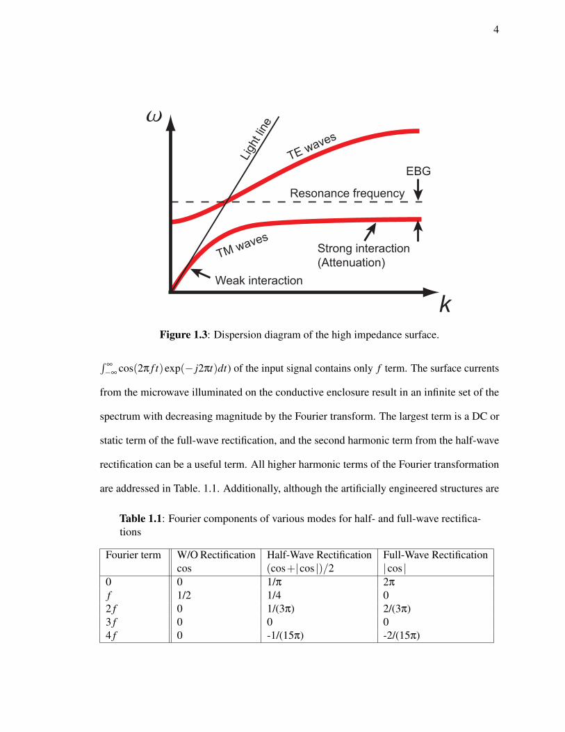
band diagram of the high impedance surface shown in Fig. 1.3 exhibits an electromagnetic
band gap (EBG). By changing the band edge, where the interaction between the surface
and wave is greatest, it may be possible to build an adaptive surface that absorbs the power
incoming signals. The nonlinear adaptivity by the diodes can be achieved by rectifying
incoming signals to static fields. The output result that has been Fourier-transformed (i.e.
4
w
k
Lig
ht lin
e
Resonance frequency
EBG
TM waves
TE waves
Weak interaction
Strong interaction
(Attenuation)
Figure 1.3: Dispersion diagram of the high impedance surface.
∫∞
−∞cos(2π f t)exp(− j2πt)dt) of the input signal contains only f term. The surface currents
from the microwave illuminated on the conductive enclosure result in an infinite set of the
spectrum with decreasing magnitude by the Fourier transform. The largest term is a DC or
static term of the full-wave rectification, and the second harmonic term from the half-wave
rectification can be a useful term. All higher harmonic terms of the Fourier transformation
are addressed in Table. 1.1. Additionally, although the artificially engineered structures are
Table 1.1: Fourier components of various modes for half- and full-wave rectifica-tions
Fourier term W/O Rectificationcos
Half-Wave Rectification(cos+|cos |)/2
Full-Wave Rectification|cos |
0 0 1/π 2π
f 1/2 1/4 02 f 0 1/(3π) 2/(3π)3 f 0 0 04 f 0 -1/(15π) -2/(15π)
5
able to work as the absorber, there will be significant scattering into free space or backward
reflections to other systems which are sharing the same platform, while the reactive coating
does not cover the entire outer structure of interest. Therefore, a new type of nonlinear
metasurface such as an adaptive absorber is needed to mitigate high surface currents for
decoupling other sensitive components of the shared conductive body.
1.2 Metamaterial Surfaces
In nature, each material has unique properties to distinguish itself. Permittivity and
permeability factors define electromagnetic properties such as wave parameters including
the index of refraction ( 1.1), corresponding wavelength ( 1.2), and wave impedance ( 1.3)
of the medium.
n =
√ε
µ(1.1)
λm =λ√
εµ(1.2)
Z =
√µε
(1.3)
The index of refraction is one of the fundamental factors to exhibit the electromag-
netic phenomena, called Snell’s law; the interactions on the interface between two different
mediums, when electromagnetic radiation is incident at an oblique angle. The indices of
refraction of all materials that exist in natural environments exhibit positive values. However,
a Russian physicist, Veselago, has theoretically reported that the negative index of refraction
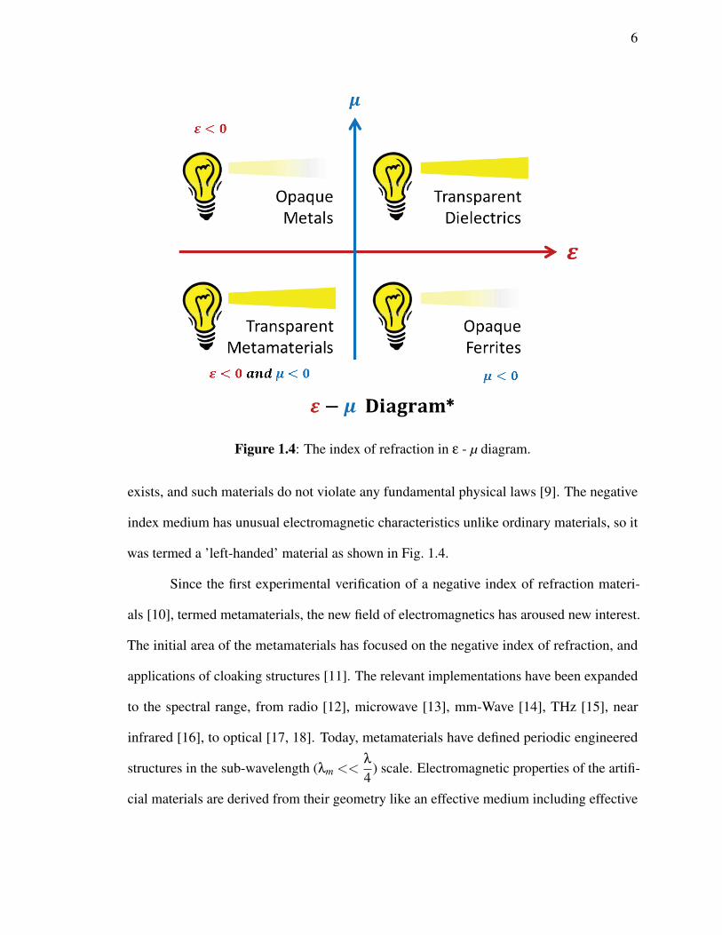
6
Figure 1.4: The index of refraction in ε - µ diagram.
exists, and such materials do not violate any fundamental physical laws [9]. The negative
index medium has unusual electromagnetic characteristics unlike ordinary materials, so it
was termed a ’left-handed’ material as shown in Fig. 1.4.
Since the first experimental verification of a negative index of refraction materi-
als [10], termed metamaterials, the new field of electromagnetics has aroused new interest.
The initial area of the metamaterials has focused on the negative index of refraction, and
applications of cloaking structures [11]. The relevant implementations have been expanded
to the spectral range, from radio [12], microwave [13], mm-Wave [14], THz [15], near
infrared [16], to optical [17, 18]. Today, metamaterials have defined periodic engineered
structures in the sub-wavelength (λm <<λ
4) scale. Electromagnetic properties of the artifi-
cial materials are derived from their geometry like an effective medium including effective
7
permittivity and permeability rather than inheriting them directly from their material compo-
sition [19]. The research agenda in the metamaterial fields is now shifting from the negative
index superlens towards the emerging field of meta-devices achieving unique and useful
functionalities such as tunable, switchable, nonlinear and sensing [20].
Among different types of metamaterials, the planar metamaterial structures, termed
as metasurfaces [21, 22, 23, 24, 25, 26], manipulate of electromagnetic waves by densely
arranged periodic structures in a two-dimensional area. The metasurface bounds the electric
and magnetic polarizations, and modifies over the reflected and transmitted waves for the
novel applications in the microwave and optical regions [27].
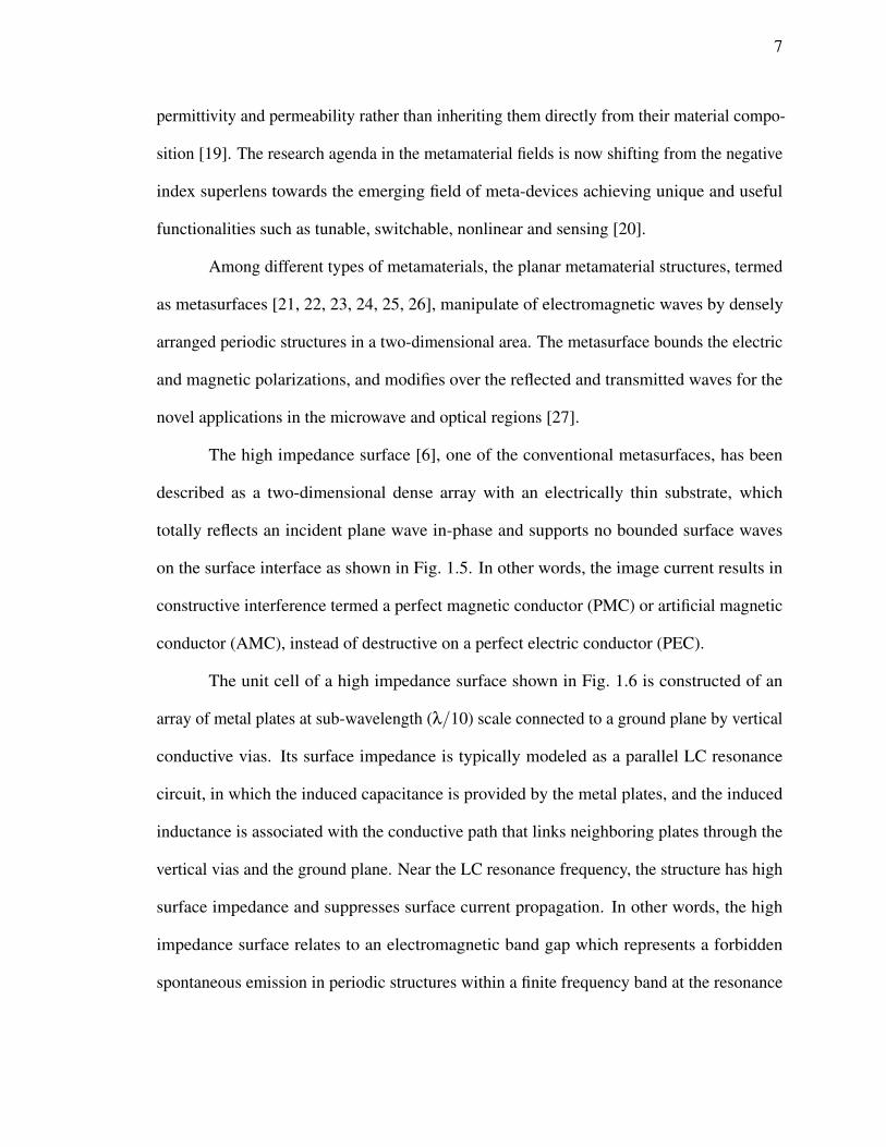
The high impedance surface [6], one of the conventional metasurfaces, has been
described as a two-dimensional dense array with an electrically thin substrate, which
totally reflects an incident plane wave in-phase and supports no bounded surface waves
on the surface interface as shown in Fig. 1.5. In other words, the image current results in
constructive interference termed a perfect magnetic conductor (PMC) or artificial magnetic
conductor (AMC), instead of destructive on a perfect electric conductor (PEC).
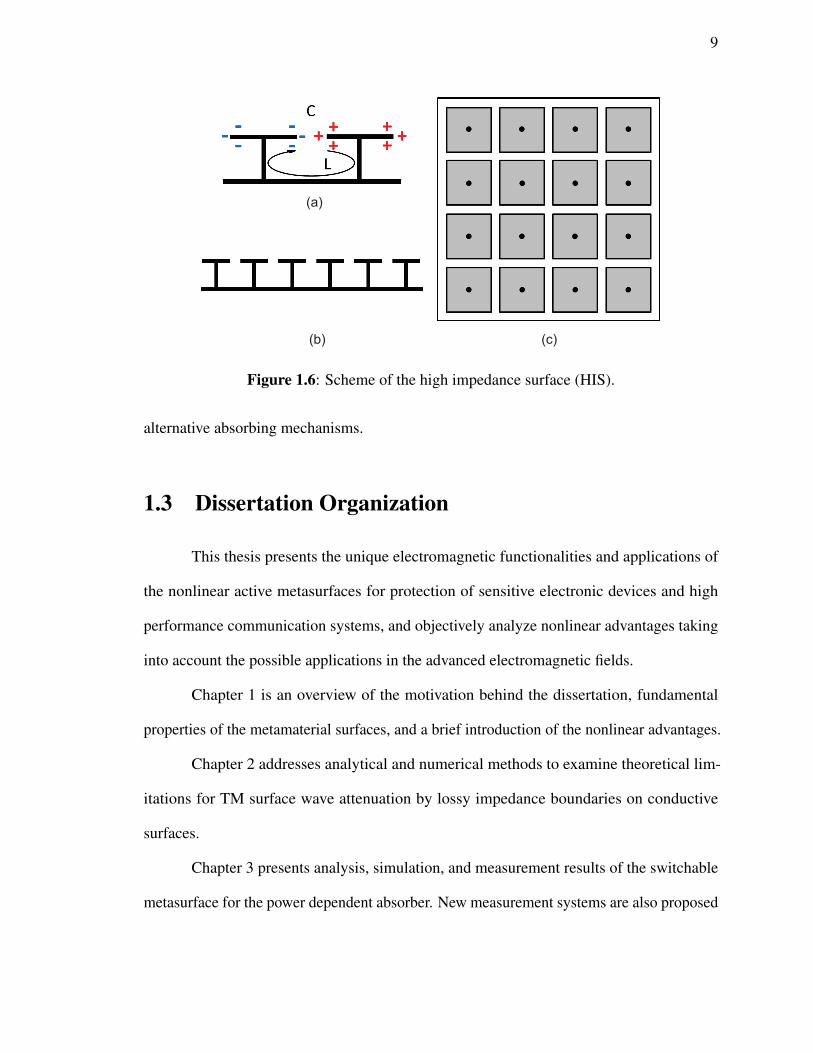
The unit cell of a high impedance surface shown in Fig. 1.6 is constructed of an
array of metal plates at sub-wavelength (λ/10) scale connected to a ground plane by vertical
conductive vias. Its surface impedance is typically modeled as a parallel LC resonance
circuit, in which the induced capacitance is provided by the metal plates, and the induced
inductance is associated with the conductive path that links neighboring plates through the
vertical vias and the ground plane. Near the LC resonance frequency, the structure has high
surface impedance and suppresses surface current propagation. In other words, the high
impedance surface relates to an electromagnetic band gap which represents a forbidden
spontaneous emission in periodic structures within a finite frequency band at the resonance

8
Figure 1.5: Artificial magnetic conductor properties of the high impedance surface.
frequency. In this regime corresponding to a high capacitive surface impedance, neither TM
nor TE surface waves are allowed to propagate on the surface, which drives an exponential
decay in both fields in the surface plane and provides considerable absorptivity in use of the
low profile absorbing structures.
The metasurfaces using a microwave absorber are limited by their narrow bandwidth,
which is generally determined by their substrate thickness. Hence, applying nonlinear
components such as diodes and transistors will give an additional degree of freedom that
cannot be easily achieved with linear materials. The proposed nonlinear active metasurfaces
can convert the incident waves into a different frequency, mode, or polarization, to allow
9
(a)
(b) (c)
Figure 1.6: Scheme of the high impedance surface (HIS).
alternative absorbing mechanisms.
1.3 Dissertation Organization
This thesis presents the unique electromagnetic functionalities and applications of
the nonlinear active metasurfaces for protection of sensitive electronic devices and high
performance communication systems, and objectively analyze nonlinear advantages taking
into account the possible applications in the advanced electromagnetic fields.
Chapter 1 is an overview of the motivation behind the dissertation, fundamental
properties of the metamaterial surfaces, and a brief introduction of the nonlinear advantages.
Chapter 2 addresses analytical and numerical methods to examine theoretical lim-
itations for TM surface wave attenuation by lossy impedance boundaries on conductive
surfaces.
Chapter 3 presents analysis, simulation, and measurement results of the switchable
metasurface for the power dependent absorber. New measurement systems are also proposed
10
to measure suppression of surface currents and leakage fields through an electrically tiny
gap.
Chapter 4 studies the concept of the self-tunability. A feedback circuit with the
slope detector and RF-DC rectifier is introduced to detect and generate the desired DC
bias to achieve the active adjustments of the self-tuning metasurface following incoming
frequencies.
Chapter 5 examines using the octave-tunability to systematically manipulate surface
impedance by MOSFET transistors. The reconfigurable ground plane can be reconfigured
to support advanced antenna systems.
Chapter 6 explores anisotropic surface topologies that exhibit all-directional re-
sponses against incoming waves.
Chapter 7 summarizes and concludes the thesis, and addresses directions for further
research.
Chapter 2
Theoretical Limitations for TM Surface
Wave Attenuation by Lossy Coatings on
Conducting Surfaces
In this chapter, the theoretical limitations for TM surface wave attenuation on
lossy coated conducting surfaces containing electric and/or magnetic loss are analyzed by
analytical and numerical methods. The proposed analytical approaches are consistent with
numerical simulation data. A simple expression to approximate a wide range of material
properties is proposed in this chapter. Furthermore, lossy slabs with simple equivalent circuit
boundaries on top are analyzed, which may be provided by frequency selective surfaces
or other patterned structures. Such composite lossy coating can exceed the attenuation
of a simple lossy slab, but with limited bandwidth. Additionally, only through increasing
permeability, and not permittivity, can the peak absorption frequency be lowered for a given
thickness without reducing the relative absorption bandwidth.
11

12
2.1 Overview of TM Surface Wave Attenuation
A grounded dielectric slab can support bound surface waves [28, 29]. The bound
waves are related to the ordinary surface currents that occur in any metal surface in the limit
where the dielectric thickness approaches zero. The surface currents contribute significantly
to interference between nearby antennas or electronics [30, 2], and suppressing the currents
such as by using a lossy coating can be an important tool for interference reduction [6,
31]. An analytical solution to the attenuation by a dielectric slab has been provided by
Attwood [32], where he calculated loss terms for both the conductor loss in the metal surface
and dielectric loss due to the slab. However, there has been no attempt to analyze general
trends or theoretical limits of the attenuation by lossy coatings, particularly for surface waves.
The most relevant general analysis is for plane waves at normal incidence [33]. Furthermore,
Attwoods original analysis cannot be applied to many modern lossy coatings that may
contain magnetic materials, as well as patterned composite materials such as frequency
selective surfaces [34] or metamaterials [35]. In this work, we extend Attwood’s analysis to
include both of these effects and we verify our analytical solution with numerical simulations.
We refer to lossy slabs that may contain impedance sheets, frequency selective surfaces
(FSS), or other such structures collectively as ”coatings.” Our analytical solution allows us to
sweep a wide range of material properties to derive general trends and establish theoretical
limits. In particular, we find that the attenuation by a lossy slab can be approximated by
a simple formula. Adding an impedance sheet on top of the slab that can be described by
an equivalent circuit can provide greater attenuation than the slab alone, but over limited
bandwidth. Thus, lossy coatings combined with frequency selective surfaces, metamaterials
or other such patterned surfaces can be effective narrowband absorbers. A transverse
magnetic (TM) type wave is assumed to be a uniform surface wave propagating parallel to
13
the surface of a dielectric slab on a conducting surface. We focus on TM waves because
most absorbing coatings are electrically thin, however because the purpose of this paper is
to establish trends, we will study a wide range of thicknesses. We follow Attwood’s analysis
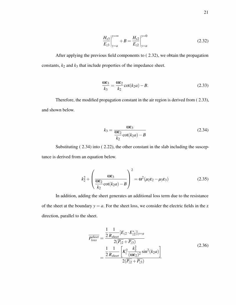
and label the conductor as region 1, the slab as region 2 and the surrounding air as region
3. In order to consider only the effects of the slab, we assume that region 1 is a perfect
electric conductor as shown in Fig. 2.1. Region 2 is a dielectric material of thickness ’a’
with relative permittivity (ε) and permeability (µ). The loss properties are represented by
the imaginary permittivity (ε′′2) and permeability (µ
′′2). In region 3, we assume the material
outside of the dielectric slab is air with relative permittivity and permeability of unity. We
also consider the case where an impedance sheet is located between the slab and the air
region. The sheet is considered to have an infinitesimal thickness such as a thin frequency
selective surface [34].
2.2 Analytical Solution
To determine the theoretical limitations of attenuation by a lossy slab, first, we
consider an analytical solution. The analytical solution is developed from Maxwell’s
equations, assuming a traveling TM surface wave. We follow Attwood’s analysis [32] and
also add the effects of magnetic loss, and lossy or reactive impedance sheets.
2.2.1 Without Impedance Sheet
For the transverse fields in the slab and air regions, we first start with Maxwell’s
equations under source-free, linear and homogeneous space conditions.

14
Figure 2.1: Geometry for TM surface wave propagating along the direction withthe electric field decaying in the y-direction. Schematic of the structure andproperties of materials; region 1 is assumed to be a perfect conductor (σ = ∞),region 2 is a slab of thickness a with loss properties, given by the imaginarycomponents of relative permittivity (ε′′2) and permeability (µ′′2), region 3 is air.There is a possible impedance sheet between the region 2 and region 3.
∇•E = 0
∇•B = 0
∇×E =− jωµH
∇×H = jωεE
(2.1)
A propagating TM surface wave along the z-direction is considered as a monochromatic
wave. The wave components are functions of y, and independent of x. Therefore, Maxwells
equations ( 2.1) are reduced to below.

15
∂Ey
∂y− jβEz = 0
∂Ez
∂y+ jβEy =− jωµHx
− jβHx = jωεEy
−∂Hx
∂y= jωεEz
(2.2)
To obtain the propagating field Ez as a wave equation, we differentiate ( 2.2) with
respect to the y direction, and then combine both equations. The equation represents the
electric field along propagating direction, Ez, as below.
∂2Ez
∂y2 =−(ω2µε−β2)Ez (2.3)
Following a similar procedure, we can derive equations for the transverse fields in
the y and x vector components, Ey and Hx, respectively.
∂2Ey
∂y2 =−(ω2µε−β2)Ey (2.4)
∂2Hx
∂y2 =−(ω2µε−β2)Hx (2.5)
From above field components, ( 2.3), ( 2.4), and ( 2.6), a propagation constant is
represented in which the wave number β which must be real. The propagation constant k
along the y-direction is given by
k2 = ω2µε−β
2 =(
ω
c
)2µrεr−β
2 (2.6)
Here, c is the speed of light.
16
We assume equations for the fields as below.
Ez =12(Ae+ jky +Be− jky)
Ey =12(Ae+ jky +Be− jky)
Hx =12(Ae+ jky +Be− jky)
(2.7)
We applied the above field equations to the structure as shown in Fig. 2.1. In the
slab, we have an equation to represent the tangential electric field at the conductor boundary
y = 0, where the boundary conditions are Ez2 = 0, and therefore B2 =−A2, where subscript
2 represents region 2, the slab. Thus, we have
Ex2 =12
A2(e+ jk2y− e− jk2y) = jA2 sin(k2y) (2.8)
In a similar manner, we have equations for the other transverse fields below.
Ey2 =12
A2β
k2(e+ jk2y + e− jk2y) = A2
β
k2cos(k2y) (2.9)
Hx2 =−12
A2ωε2
k2(e+ jk2y + e− jk2y) =−A2
ωε2
k2cos(k2y) (2.10)
From ( 2.8), ( 2.9), and ( 2.10), we see that inside the slab the unattenuated field
components are sinusoidally distributed in the z-direction. On the other hand, in the air
region the fields are exponentially decaying in the y-direction, so k3 is imaginary and B3 = 0
, where subscript 3 represents region 3, the air region.
Ez3 = (A3e+ jk3y +B3e− jk3y)
= jA3e− jk3y(2.11)

17
The electric field in ( 2.8) and ( 2.11) must be same at the dielectric boundary y = a,
so A3 can be represented in terms of A2.
A3 = A2e+k3a sin(k2a) (2.12)
Therefore, we have an equation for the electric field at the air region in z-direction.
Ez3 =+ jA2e+k3a sin(k2a)e−k3y (2.13)
By using similar methods, we can obtain transverse fields in the air region, Ey3
and Hx3 respectively. From ( 2.10) by considering Kz =−A2(ωε2/k2) we rewrite the field
components on both dielectric regions, below. For the dielectric slab in region 2,
Eslabz2 = jKz
k2
ωε2sin(k2y), (2.14)
Eslaby2 = Kz
β
ωε2cos(k2y), (2.15)
Hslabx2 =−Kzcos(k2y). (2.16)
For the air in region 3,
Eairz3 = jKz
k2
ωε2exp+k3a sin(k2a)exp−k3y, (2.17)
Eairy3 = Kz
k2
k3
β
ωε2exp+k3a sin(k2a)exp−k3y, (2.18)
18
Hairx3 =−K
k2
k3
ε3
ε2exp+k3a sin(k2a)exp−k3y . (2.19)
Here, Kz is an amplitude of tangential component in ( 2.15) of the slab, Kz ∝
−(ωε2/k2). The relations between the propagation factor, permittivity, permeability and fre-
quency in both regions are developed from the wave equation. The relations are represented
below.
k22 = ω
2µ2ε2−β2, (2.20)
( jk3)2 =−k2
3 = ω2µ3ε3−β
2, (2.21)
k22 + k2
3 = ω2(µ2ε2−µ3ε3). (2.22)
At the boundary, y = a, the impedance is continuous, because the tangential com-
ponents of electric field E and magnetic field H are continuous. From this condition, the
propagation constant in the air region is represented as below.
k3 = k2ε3
ε2tan(k2a) (2.23)
Substituting ( 2.23) into ( 2.22), we obtain an equation for the propagation constant
in the slab.
k22
[1+
ε23
ε22
tan2(k2a)]= ω(µ2ε2−µ3ε3) (2.24)
Using the above relations, we can solve for β, k2 and k3 from ( 2.21), ( 2.24) and
19
( 2.23). In formulating an equation for the attenuation by the loss properties of the slab, we
had to consider the fields in both dielectric and air regions. The attenuation is proportional
to the time average loss in the slab and to the time average power of the wave propagating
in both regions. To obtain the time average power propagating along the z-direction, we
determine the time average Poynting vector in both regions.
Pz =−12
∫ y=a
y=0Re[Ey2H∗x2]dy− 1
2
∫ y=∞
y=aRe[Ey3H∗x3]dy (2.25)
In ( 2.25), the first term represents the time average power in the slab, and the second
term represents the time average power of the air region. Each field components are from
( 2.15), complex conjugate of ( 2.15), ( 2.17), and complex conjugate of ( 2.18). Hence, in
each region, the time average propagating power is derived as below. For the slab,
Pslabz2 =+K2
z1
4k2
β
ωε2
[k2a+
12
sin(2k2a)]. (2.26)
For the air region,
Pairz3 =+K2
z14
ε3
ε2
k22
k33
β
ωε2sin2(k2a). (2.27)
To obtain the time average loss in the slab including both dielectric and magnetic
loss, we calculate the real power dissipated in the slab.
Ploss =∫ y=a
y=0
[ω
2ε′′|E|2 + ω
2µ′′|H|2
]dy
=∫ y=a
y=0
[ω
2ε′′(Ey2 ·E∗y2 +Ez2 ·E∗z2)+
ω
2µ′′(Hx2 ·H∗x2)
]dy
(2.28)
In ( 2.28), the first term is for electrical loss and the second is for magnetic loss,
respectively. Each field components are from ( 2.14), complex conjugate of ( 2.16), ( 2.17),

20
and complex conjugate of ( 2.18). Hence, the loss of time average propagating power in the
slab with dielectric and magnetic loss properties is given below.
Pslabloss =+K2
zωε′′
4(ωε)2
[(β2 + k2
2)a+β2− k2
22k2
sin(2k2a)]
+K2z
ωµ′′
4
[1
2k2sin(2k2a)+a
] (2.29)
Finally, the attenuation of TM surface waves on a lossy slab is given by
α =Pslab
loss
2(Pslabz2 +Pair
z3 )(2.30)
2.2.2 With Impedance Sheet
In the case of applying the impedance sheet to the top of the slab, we assume it is
represented by an equivalent transmission line system in which the slab, the impedance
sheet and the air region are connected in parallel. To develop an analytical solution for the
attenuation with the impedance sheet, we need to calculate modified propagation constants
for both the slab and air regions. The transverse resonance method (TRM) [28, 36] has
been used to calculate the modified propagation constants with the impedance sheet. The
propagation constants that satisfy the TRM are determined by equating the admittance
looking down into the slab, and up into the air region, including the susceptance component
of the impedance sheet [37].
Y air + susceptanceo fY sheet = Y slab (2.31)
We can construct an equation at the boundary that is expressed in terms of the field
components in both slab and air regions and the susceptance B of Y sheet as shown in Fig. 2.1.
21
Hx3
Ez3
∣∣∣∣y=∞
y=a+B =
Hx2
Ez2
∣∣∣∣y=0
y=a(2.32)
After applying the previous field components to ( 2.32), we obtain the propagation
constants, k2 and k3 that include properties of the impedance sheet.
ωε3
k3=
ωε2
k2cot(k2a)−B. (2.33)
Therefore, the modified propagation constant in the air region is derived from ( 2.33),
and shown below.
k3 =ωε3
ωε2
k2cot(k2a)−B
(2.34)
Substituting ( 2.34) into ( 2.22), the other constant in the slab including the suscep-
tance is derived from an equation below.
k22 +
ωε3ωε2
k2cot(k2a)−B
2
= ω2(µ2ε2−µ3ε3) (2.35)
In addition, adding the sheet generates an additional loss term due to the resistance
of the sheet at the boundary y = a. For the sheet loss, we consider the electric fields in the z
direction, parallel to the sheet.
Psheetloss =
12
1Rsheet
[Ez2 ·E∗z2]|y=a
2(Pz2 +Pz3)
=
12
1Rsheet
[K2
zk2
2(ωε2)2 sin2(k2a)
]2(Pz2 +Pz3)
(2.36)

22
Therefore, the sheet loss can be linearly added to the total attenuation, α, as given
below.
α =Pslab
loss +Psheetloss
2(Pslabz2 +Pair
z3 )(2.37)
By applying the TRM to calculate the modified propagation constants, we now have an
expression for the attenuation which includes the properties of the impedance sheet on the
top of the slab. In the case of applying an impedance boundary to the sheet, the susceptance
B is given by
Ysheet = G+ jB =1
Zsheet=
1R+ jX
(2.38)
Table 2.1: Summary of analytical solutions
Time average propagat-ing power in slab region Pslab
z2 =+K2z
14k2
β
ωε2
[k2a+
12
sin(2k2a)]
Time average propagat-ing power in the air re-gion
Pairz3 =+K2
z14
ε3
ε2
k22
k33
β
ωε2sin2(k2a)
Time average powerloss in the slab region Pslab
loss =+K2z
ωε′′
4(ωε)2
[(β2 + k2
2)a+β2− k2
22k2
sin(2k2a)]
+K2z
ωµ′′
4
[1
2k2sin(2k2a)+a
]Impedance surface (Zs) Without Zs With Zs
Transvers ResonanceMethod (TRM)
Hx3
Ez3
∣∣∣∣y=∞
y=a+B =
Hx2
Ez2
∣∣∣∣y=0
y=a
Time average powerloss in the impedancesheet
Psheetloss =
12
1Rsheet
[K2
zk2
2(ωε2)2 sin2(k2a)
]2(Pz2 +Pz3)
Attenuation α =Pslab
loss
2(Pslabz2 +Pair
z3 )α =
Pslabloss +Psheet
loss
2(Pslabz2 +Pair
z3 )
23
G =R
R2 +X2
B =− XR2 +X2
(2.39)
The analytically summarized field solutions to the each region, and attenuations are listed in
Table. 2.1.
We assume that the dielectric slab and ground plane provide inductance, so our
analysis focuses on sheets having resistance and capacitance, and we consider both series
and parallel RC circuits for the impedance sheet. In the parallel connection of resistance
and capacitance, the susceptance is given by
Ysheet = G+ jB = YR +YC
=1R+ jωC
(2.40)
G =1R
B = ωC(2.41)
In series connection between resistance and capacitance, the susceptance is given by
Zsheet = ZR +ZC = R− j1
ωC(2.42)
Ysheet =1
Zsheet= G+ jB =
R
R2 +
(1
ωC
)2 + j
1ωC
R2 +
(1
ωC
)2 (2.43)
24
G =R
R2 +
(1
ωC
)2
B =
1ωC
R2 +
(1
ωC
)2
(2.44)
Using the susceptances of ( 2.39), ( 2.41), and ( 2.44) under each condition, the
analytical solution for attenuation is modified to include the properties of various kinds of
impedance sheets.
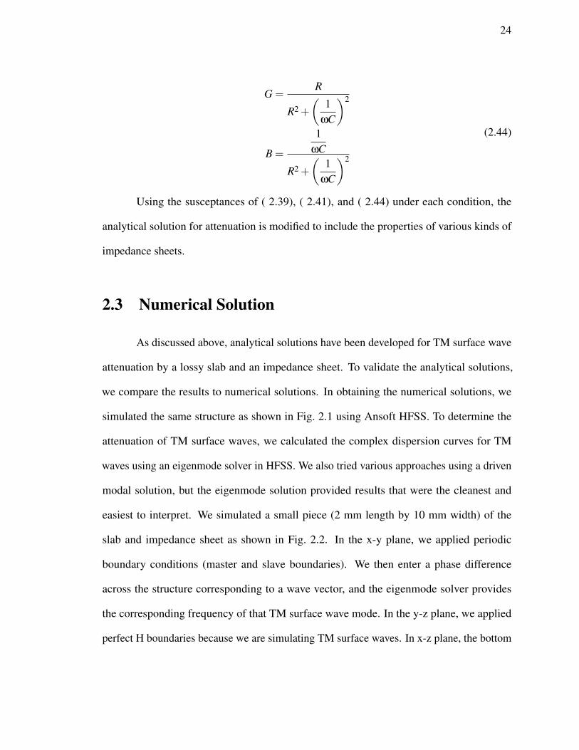
2.3 Numerical Solution
As discussed above, analytical solutions have been developed for TM surface wave
attenuation by a lossy slab and an impedance sheet. To validate the analytical solutions,
we compare the results to numerical solutions. In obtaining the numerical solutions, we
simulated the same structure as shown in Fig. 2.1 using Ansoft HFSS. To determine the
attenuation of TM surface waves, we calculated the complex dispersion curves for TM
waves using an eigenmode solver in HFSS. We also tried various approaches using a driven
modal solution, but the eigenmode solution provided results that were the cleanest and
easiest to interpret. We simulated a small piece (2 mm length by 10 mm width) of the
slab and impedance sheet as shown in Fig. 2.2. In the x-y plane, we applied periodic
boundary conditions (master and slave boundaries). We then enter a phase difference
across the structure corresponding to a wave vector, and the eigenmode solver provides
the corresponding frequency of that TM surface wave mode. In the y-z plane, we applied
perfect H boundaries because we are simulating TM surface waves. In x-z plane, the bottom

25
Figure 2.2: Schematic for the numerical solutions and assigned boundaries. Inthe x− y plane, master and slave boundaries are applied, in the y− z plane, perfectmagnetic conductor (PMC) boundaries are applied, in the x− z plane, perfectelectric conductor (PEC) boundaries are applied.
and top planes are perfect E boundaries with 50 mm height between the planes including 10
mm height of the slab. At the surface of the dielectric slab, we applied an impedance sheet
or lumped RLC boundary. In the slab, we used a material with relative complex permittivity
and permeability. The relative complex values, εr = 10+ j0.001 and µr = 1+ j0.001 are
used in most simulations. Also, we examined a wide variety of material properties in this
study. At the impedance sheet, using the lumped RLC boundary, a range of resistance and
capacitance were studied. As part of the eigenmode solution, we also obtain the quality
factor Q of each mode which is a function of the real and imaginary parts of frequency, ω
and ω′′.
26
Q =
∣∣∣∣ ω′
2ω′′
∣∣∣∣ (2.45)
This definition of Q indicates that it is a measure of how quickly the mode would
decay in time if it were excited uniformly across the surface at some starting time, and
then allowed to decay without additional excitation. However, what we need is the rate of
decay along the surface for a wave starting at one end with continuous excitation. These
two quantities are related through the group velocity of the wave, which itself is a function
of frequency.
α =ω′′
νg= ω
′′ dkdω
(2.46)
Here, k is the wave number, and ω and ω′′
represent real and imaginary angular
frequencies, respectively. The magnitude of electric field decreases along the length of the
surface by E ∝ exp− jkz. Therefore, the modified wave number can be expressed by k = φ/z.
Here z is the length of the structure in our simulation, and φ is the phase difference applied
to the periodic boundary conditions in the z-direction. Substituting ( 2.45) and the modified
wave number into ( 2.46) gives the equation for attenuation using calculated values in the
HFSS eigenmode solver, and then we numerically differentiate to obtain
α = ω′′ dk
dω=
ω′
2Q1z
dφ
dω=
ωn+1
2Q1z
φn+1−φn
ωn+1−ωn(2.47)
Where n and n+1 represent two successive simulations.

27
2.4 Results
2.4.1 Validation of Analytical Solution
0 2 4 6 8 10
0
20
40
60
80
.
Frequency [GHz]
Att
en
ua
tio
n [
1/m
]
Analytical Solution
Numerical Solution
TM0
TM1
TM2
Figure 2.3: Matching plot between the analytical and numerical solutions with animpedance sheet on the slab of dielectric loss 0.001 and magnetic loss 0.001 withresistance of 377Ω/square and reactance of 1Ω/square, respectively.
In previous sections, we discussed the analytical and numerical solutions, separately.
To verify the analytical solutions, we have performed a detailed comparison with the
numerical solutions from HFSS simulations. The matching plot shown in Fig. 2.3 is
representative of a range of different conditions. In the plot, the impedance sheet is modeled
as a series RC circuit, but we have also checked the parallel case for consistency. Multiple
peaks in the plot correspond to different TM surface waves and are labeled T M0, T M1,
etc. In the plot, the solid lines represent the analytical solutions and the dots represent the
numerical solutions. Because of the close agreement between the analytical and numerical
solutions for a wide range of properties for the slab and the impedance sheet, we are
28
0 2 4 6 8 100
0.5
1.0
1.5
2.0
Frequency @GHzD
Atte
nuat
ion@1mD
Slab Only
Envelope Limit Line
U = 1.2
Figure 2.4: Envelope limit line for the dielectric slab without any impedance sheet.Properties of the dielectric slab are the relative permittivity 10, permeability 2,dielectric loss tangent 0.001 and magnetic loss tangent 0.001 with thickness 1 cm.The unit factor, U , of the enveloped limit line is 1.2.
convinced that the analytical solution for the attenuation is formulated correctly.
2.4.2 Theoretical Limitations
After having validated our analytical model, we now explore a wide range of material
and impedance sheet properties to identify trends and limits. For the following discussion,
we initially consider the case where there is no impedance sheet on the slab. In every case,
we find that the attenuation shows a series of peaks corresponding to the surface wave modes,
and that these peaks form an envelope that can be approximated by a linear function that is
consistent over a wide range of material properties. An example is shown in Fig. 2.4. We
designated the line as the ’envelope limit line’ which is given by
α∼= U · f · ε2 ·µ2 · tanδ (2.48)
29
0 2 4 6 8 100
2
4
6
8
10
Frequency @GHzD
Atte
nuat
ion@1mD
Series
Parallel
Slab Only
Envelope Limit Line
U = 1.3
Parallell
Series
Figure 2.5: Comparison of attenuation values when adding an impedance sheetto the dielectric slab: the dashed line shows the envelope limit line with U = 1.3.the solid and the dot dashed lines show parallel and series impedance sheets,respectively, with resistance of 1000Ω/square and capacitance of 0.1 pF/square.Note that we have only plotted the first of a series of attenuation peaks.
0 0.2 0.4 0.6 0.8 1.00
1
2
3.
Capacitance @pFsquareD
Fre
quen
cy@G
HzD Resistance 1000 Wsquare
Resistance 377 Wsquare
Resistance 100 Wsquare
Figure 2.6: Peak frequency as a function of the capacitance of an impedance sheetin parallel connection of resistance and capacitance values. The dot dashed line,dashed line, and solid line represent different sheet resistances of 100, 377 and1000Ω/square , respectively.
30
0 2 4 6 8 100
10
20
30
40
50
Frequency @GHzD
Atte
nuat
ion@1mD
Thickness 2.0 cm
Figure 2.7: Attenuation value for different thickness of the slab with an impedancesheet having resistance of 377Ω/square and capacitance of 0.1 pF/square. Thethicknesses of the slab are 0.5 and 2.0 cm, respectively.
0 0.2 0.4 0.6 0.8 1.00
0.2
0.4
0.6
0.8
1.
Capacitance @pFsquareD
Rel
ativ
eba
ndw
idth
Thickness 2.0 cm
Thickness 1.0 cm
Figure 2.8: Relative bandwidth for different thicknesses of the slab as a functionof capacitance. This is for an impedance sheet represented by a parallel RC circuit.
tanδ =µ2ε
′′2 +µ
′′2ε2
µ2ε2−µ′′2ε′′2
(2.49)

31
0 20 40 60 80 1000
0.5
1.0
1.5
2
x HΕr or Μr L
Rel
ativ
eba
ndw
idth
Εr = x, Μr = any
Μr = x, Εr = 2
Μr = x, Εr = 5
Μr = x, Εr = 10
Figure 2.9: Relative bandwidth for different slab properties as a function of relativepermittivity or permeability up to 100. The solid, dot dashed and dashed lines arefor swept relative permeability with the fixed permittivity of 2, 5 and 10. The thicksolid line represents a swept relative permittivity with a permeability of 10.
0 200 400 600 800 10000.1
1
10
102
103
104.
Resistance @WsquareD
Atte
nuat
ion@1mD
Capacitance 0.1 @pFsquareD
0 200 400 600 800 10000.1
1
10
102
103
104.
Resistance @WsquareD
Atte
nuat
ion@1mD
Capacitance 1.0 pFsquare
Capacitance 0.1 pFsquare
0.1 pF/square
1.0 pF/square
Α = 0.1 (slab only)
Figure 2.10: Peak attenuation values as a function of resistance of the impedancesheet, which is represented by a parallel RC circuit. The solid and dot dashed linesrepresent different capacitances, 0.1 and 1.0 pF/square, respectively. The dashedline represents the envelope limit line for the slab alone.

32
Here, f and c represent frequency and speed of light in free space, and loss tangent,
tanδ expressed in ( 2.49) [38], represents the combined dielectric and magnetic loss
properties. In ( 2.48), there is a factor, U, which has a value that is approximately unity for a
wide range of material properties, and can be considered to be unity as a simple guideline
for estimating attenuation.
Even under a broad range of loss tangents from 0.001 to 1.0, U is still within this
range. When the slab is electrically thick, the attenuation deviates from ( 2.48), but only by
a small amount. Thus, ( 2.48) provides a valuable guideline for estimating attenuation. It is
noteworthy that the thickness does not affect the slope of the envelope limit line, although
the thickness does determine the frequency of the first mode, and the frequency spacing of
the modes.
If an impedance sheet is added to the slab, the attenuation can be substantially greater
than the envelope limit line as shown in Fig. 2.5, but over limited bandwidth. The peak
frequency is determined by the capacitance of the sheet and thickness of the slab, as shown
in Fig. 2.6 and 2.7, while the maximum attenuation value is determined by the resistance of
the sheet, and the thickness and loss parameters of the slab. Increasing the slab thickness
reduces the peak frequency, but also reduces the absolute bandwidth of the peak, as shown
in Fig. 2.7, as measured by the full width at half maximum (FWHM).
Thus, the relative bandwidth, as determined by the absolute bandwidth at the FWHM
divided by the peak frequency, is essentially independent of the slab thickness and the
properties of the sheet, as shown in Fig. 2.8. The permeability and permittivity of the slab
affect the relative bandwidth in different ways, as shown in Fig. 2.9.
Increasing either of these parameters will reduce the peak absorption frequency.
However, increasing permeability does so without affecting the relative bandwidth, which
33
increasing permittivity substantially reduces relative bandwidth. This is consistent with
previous studies of absorption of normally incident waves [33], where permeability has a
beneficial effect on bandwidth, but permittivity does not.
Although the resistance of the sheet does not significantly affect the peak frequency
or bandwidth, it does affect the maximum attenuation value. The attenuation values of
the peak of the first curve are related to the resistance of the impedance sheet as shown
in Fig. 2.10. In the plot, the value of the attenuation decreases with increasing resistance.
Additionally, the curves for the attenuation values with the impedance sheet are compared
to a dashed straight line corresponding to the envelope limit line of the slab only. Thus, the
impedance sheet can enhance the attenuation compared to the slab alone, but at the expense
of bandwidth.
2.5 Conclusion
We have developed an analytical model for TM surface wave attenuation by grounded
lossy slabs including both dielectric and magnetic losses. Using the transverse resonance
method we have extended the solution to include an impedance sheet which may represent
a FSS, metasurface or other periodic structure. We find that for the case of the bare slab,
the attenuation can be approximated by a simple formula for a wide range of material
properties. By making practical assumptions about available materials, this formula can be
used to estimate the limits on absorption for homogeneous linear lossy slabs. We have also
found that the use of an impedance sheet can provide substantially greater attenuation than
what is possible with a simple lossy slab, but with limited bandwidth. For an impedance
sheet that can be described in terms of effective sheet capacitance and sheet resistance, the
capacitance and the slab thickness primarily determine the frequency of the attenuation peak,

34
and the resistance determines the maximum value of attenuation. Although the absolute
bandwidth is determined by both the capacitance of the sheet and the thickness of the slab,
the relative bandwidth is nearly independent of all of these parameters. Furthermore, increas-
ing permittivity to reduce the peak absorption frequency also reduces relative bandwidth,
whereas increasing permeability does not. These results can be used as a guideline for the
development of broadband or narrowband coatings for attenuation of TM surface waves.
Chapter 2 is based on and is mostly a reprint of the following paper: S. Kim, D.
Sievenpiper, ”Theoretical Limitations for TM Surface Wave Attenuation by Lossy Coatings
on Conductive Surfaces”, IEEE Transactions on Antennas and Propagation, vol. 62, no.1,
pp.475-480, January 2014. The dissertation author was the primary author of the work in
this chapter, and the co-author has approved the use of the material for this dissertation.

Chapter 3
Switchable Nonlinear Metasurfaces for
Absorbing High Power Surface Waves
In this chapter, a new concept of a nonlinear metamaterial surface is introduced,
which provides power dependent absorption of incident surface waves. The metasurface
includes nonlinear circuits which transform it from a low loss to high loss state when
illuminated with high power waves. The proposed surface allows low power signals to
propagate but strongly absorbs high power signals. It can potentially be used on enclosures
for electric devices to protect against damage. We experimentally verify that the nonlinear
metasurface has two distinct states controlled by the incoming signal power. We also
demonstrate that it inhibits the propagation of large signals and dramatically decreases the
field that is leaked through an opening in a conductive enclosure.
35

36
3.1 Overview of Concept
The high power surface currents are capable of leaking inside through gaps or open-
ings in the conductive shielding. Even if an aperture is electrically small, it can effectively
behave as a slot antenna that can allow radiation inside. Conventional approaches [39, 40]
to inhibit such destructive interference include applying a lossy coating on the outer surface
of the metallic shielding. Another method is to use a resonant absorber such as a Salisbury
screen [41], Jaumann absorber [42], or metamaterial absorber [8, 43, 44, 45] to absorb
incoming waves. Such conventional approaches based on linear materials absorb low power
and high power signals equally. Thus, they can reduce the performance of antennas located
on the surface, and can affect the operation of a low power communication system. Moreover,
surface currents are not entirely suppressed, and absorbing coatings can be characterized by
their attenuation rate which depends on the thickness and the materials that make up the
absorber [46]. One advantage of a nonlinear absorber is that it can decouple the attenuation
of potentially damaging high power signals from the attenuation of low power signals that
are needed for communication.
Here, we introduce the concept of a switchable metamaterial absorber based on
nonlinear circuits integrated into a high impedance surface [6]. These surfaces are electrically
thin, typically ≤ λ/10 where λ is the free space wavelength.
Nonlinear metasurfaces which respond to the waveform and power of the incoming
wave have previously been demonstrated [47, 48, 49]. Compared to prior works, this
structure provides high power absorption regardless of the incoming waveform using a
much simpler circuit, requiring only a single diode per cell, and no reactive components.
Furthermore, we demonstrate nonlinear attenuation of surface waves over a large area, and
suppressed leakage of high power signals through a narrow gap by surrounding it with a
37
nonlinear coating. We demonstrate this nonlinear absorber through electromagnetic/circuit
co-simulation, validated by measurements of small samples inside waveguides, followed by
large-area field measurements, and finally a measurement of the reduction of electromagnetic
fields entering an enclosure. Our measurements show surface wave attenuation that exceeds
that of a conventional linear absorber, and the use of such a surface for practical applications.
3.2 Mechanism of Switchable Metasurface
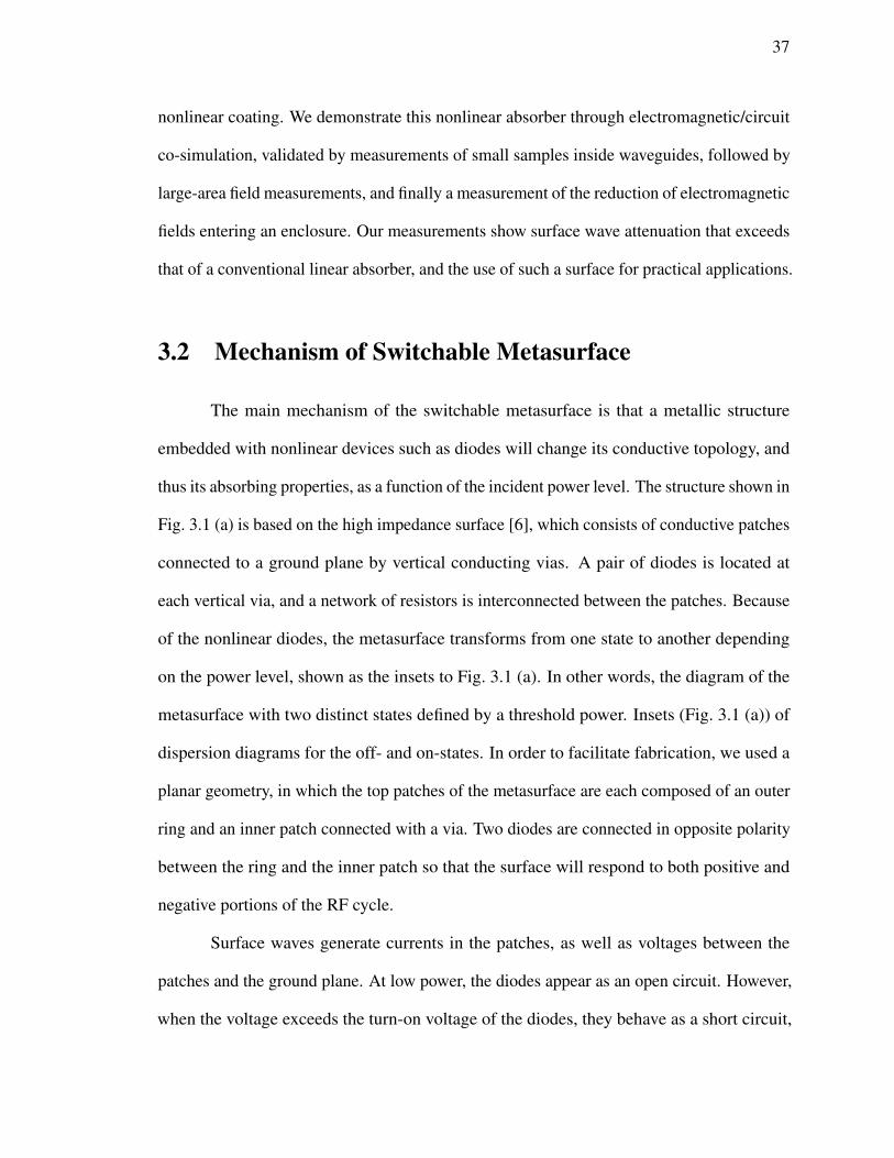
The main mechanism of the switchable metasurface is that a metallic structure
embedded with nonlinear devices such as diodes will change its conductive topology, and
thus its absorbing properties, as a function of the incident power level. The structure shown in
Fig. 3.1 (a) is based on the high impedance surface [6], which consists of conductive patches
connected to a ground plane by vertical conducting vias. A pair of diodes is located at
each vertical via, and a network of resistors is interconnected between the patches. Because
of the nonlinear diodes, the metasurface transforms from one state to another depending
on the power level, shown as the insets to Fig. 3.1 (a). In other words, the diagram of the
metasurface with two distinct states defined by a threshold power. Insets (Fig. 3.1 (a)) of
dispersion diagrams for the off- and on-states. In order to facilitate fabrication, we used a
planar geometry, in which the top patches of the metasurface are each composed of an outer
ring and an inner patch connected with a via. Two diodes are connected in opposite polarity
between the ring and the inner patch so that the surface will respond to both positive and
negative portions of the RF cycle.
Surface waves generate currents in the patches, as well as voltages between the
patches and the ground plane. At low power, the diodes appear as an open circuit. However,
when the voltage exceeds the turn-on voltage of the diodes, they behave as a short circuit,

38
Γ Χ Μ Γ0
2
4
6
8
O State
Fre
qu
en
cy [
GH
z]
Γ Χ Μ Γ0
2
4
6
8
O State
Fre
qu
en
cy [
GH
z]
! !
M
G C
E
H k
(a)
(b) (c)
(d) PMC PEC
PMC
PECcascade 9 unit cells
E
kH
- - + + - - + + - - + + - -
L
C
L L
C CC C C
Γ Χ Μ Γ0
2
4
6
8
On State
Fre
qu
en
cy [
GH
z]
Γ Χ Μ Γ0
2
4
6
8
On State
Fre
qu
en
cy [
GH
z]
E k
H
p
a g
b
cd
r
t
Lig
ht lin
e Lig
ht lin
e
"#
Figure 3.1: Nonlinear metasurfaces for power dependent absorption: (a) Diagramof the metasurface with two distinct states defined by a threshold power. Insets ofdispersion diagrams for the off- and on-states. (b) Geometry of the unit cell p = 17,t = 3.175, g = 2, a = 15, b = 4.49, c = 2.762, d = 0.864, and r = 1.0 (all in mm).(c) A photograph of the sample with circuit components attached. (d) A simulationmodel with a cascade of nine unit cells in a row with perfect magnetic conducting(PMC) walls to simulate a 2-D array.
connecting the patches to the ground plane. In this state, the surface behaves as an artificial
magnetic conductor, with an inductive current path (L) through the vias and a capacitance
39
(C) defined by the gaps between the patches. The LC resonance of the structure creates high
surface impedance [6], and the dispersion curve bends over to become flat, shown as the
inset of the on-state in Fig. 3.1 (a). Near the LC resonance frequency of around 2 GHz,
the surface waves are highly confined to the surface and interact strongly with the metallic
structure. Near the band edge, the surface waves are also strongly absorbed by the resistors
that are connected between the patches. In contrast, if the voltage on the patches does not
exceed the turn-on voltage of the diodes, the surface appears as a simple capacitive sheet
on a grounded dielectric substrate, and losses in the resistors are not significantly enhanced
without the LC resonance.
The nonlinear metasurface is implemented as shown in Fig. 3.1 (b). Geometry of the
unit cell is shown: p = 17, t = 3.175, g = 2, a = 15, b = 4.49, c = 2.762, d = 0.864, and
r = 1.0 (all in mm). Periodic conductive patterns are printed on a Rogers 5870 substrate
with a 3.175 mm thickness and with a 17 mm period as shown in Fig. 3.1 (c). Eigenmode
simulations of a single unit cell provide the band diagrams for the off- and on-states shown
in the insets of Fig. 3.1 (a). EM/circuit co-simulation of a periodic array of cells was
used to determine the absorption properties. A pair of Schottky diodes packaged together
(Avago HSMS-286C with parasitic of a series resistance 6 Ω, lead frame inductance 0.2
nH, coupling capacitance 0.035 pF, bond wire inductance 0.7 nH, package capacitance 0.03
pF, and lead frame capacitance 0.01.) was attached at each via, and 220 Ω resistors were
attached between the patches. In these simulations, a row of 9 unit cells was simulated inside
a transverse electromagnetic (TEM) waveguide constructed with perfect electric conducting
(PEC) and perfect magnetic conducting (PMC) boundaries on opposing walls of the guide
as shown in Fig. 3.1 (d). The TEM waveguide measured 17 mm wide to fit one unit cell,
and 54.6 mm in height.

40
3.3 Measurement of Nonlinear Metasurface
3.3.1 Linear Measurement in Waveguides
Figure 3.2: Measurement setup for linear waveguide measurement.
The measurement samples were fabricated with the same geometry as the simulation
model, except with a sufficient number of lateral cells to fit within a standard rectangular
metal TE waveguide. Two separate waveguide sizes (WR284 and WR430) were required to
cover the frequency range from 1.7 to 4 GHz. The resulting sample sizes were 4 x 9 cells,
and 6 x 9 cells. Transmission and reflection were measured using power meters (Agilent
N1911A) with high power signals provided by RF amplifiers (Ophir 5022 and 5193). Note
that although TEM waveguide was used in the simulation, and TE waveguide was used in
the measurement, both have similar electric and magnetic field profiles, and can be expected
to identify similar performance trends [47, 48]. TEM waveguide allows a much simpler
simulation, but the required boundary conditions are not available for experiments. The
measurement setup under the linear waveguides is shown in Fig. 3.2. The metasurface is
located at the bottom of the waveguide, and the incident wave propagates from the input

41
1 2 3 40
0.2
0.4
0.6
0.8
1
Frequency [GHz]
Re
lati
ve
ma
gn
itu
de
1 2 3 40
0.2
0.4
0.6
0.8
1
Frequency [GHz]
Re
lati
ve
ma
gn
itu
de
Absorption
Re!ection
Transmission
1 2 3 40
0.2
0.4
0.6
0.8
1
Frequency [GHz]
Re
lati
ve
ma
gn
itu
de
1 2 3 40
0.2
0.4
0.6
0.8
1
Frequency [GHz]
Re
lati
ve
ma
gn
itu
de
1 2 3 40
0.2
0.4
0.6
0.8
1
Frequency [GHz]
Re
lati
ve
ma
gn
itu
de
Absorption
Re!ection
Transmission
(a)
(b)
0 2 40
0.5
1
Time [ns]
No
rm. p
ow
er
0 2 40
0.5
1
Time [ns]
No
rm. p
ow
er
Inc. Tran. O" Tran. On
Figure 3.3: Transient simulation data, absorption (black line), reflection (red line),and transmission (blue line), are shown for (a) on-state and (b) off-state. Inset to(b) shows the comparison of normalized transmitted powers in the time domain.
port of the waveguide. The input signals are generated by the signal generator and amplified
to the high power microwaves.
The simulation and measurement results are shown in Fig. 3.3 and 3.4, respectively.
Absorption was calculated as A(ω) = 1 - T(ω) - R(ω) (A(ω): absorption, T(ω): transmission,

42
0 0.1 1 10 350
0.2
0.4
0.6
0.8
1
Power [W]
Re
lati
ve
ma
gn
itu
de
Freq. 2.4 GHz
0 0.1 1 10 350
0.2
0.4
0.6
0.8
1
Power [W]
Re
lati
ve
ma
gn
itu
de
Freq. 2.4 GHz
0 0.1 1 10 350
0.2
0.4
0.6
0.8
1
Power [W]
Re
lati
ve
ma
gn
itu
de
0 0.1 1 10 350
0.2
0.4
0.6
0.8
1
Power [W]
Re
lati
ve
ma
gn
itu
de
Freq. 2.4 GHz
1.5 2 2.5 3 3.5 40
0.2
0.4
0.6
0.8
1
Frequency [GHz]
Re
lati
ve
ma
gn
itu
de
On state
O! state
P 32W
P 10mW
1.5 2 2.5 3 3.5 40
0.2
0.4
0.6
0.8
1
Frequency [GHz]
Re
lati
ve
ma
gn
itu
de
On state
O! state
P 32W
P 10mW
1.5 2 2.5 3 3.5 40
0.2
0.4
0.6
0.8
1
Frequency [GHz]
Re
lati
ve
ma
gn
itu
de
1.5 2 2.5 3 3.5 40
0.2
0.4
0.6
0.8
1
Frequency [GHz]
Re
lati
ve
ma
gn
itu
de
On state
O! state
P 32W
P 10mW
(a)
(b)
Figure 3.4: Simulation and measurement of the nonlinear metasurface inside thewaveguides. The surface demonstrates two distinct states for low and high powerconditions. (a) Dashed and solid dotted lines represent transient simulation andmeasurement data, respectively. (b) Absorption at 2.4 GHz versus incoming powerlevels.
and R(ω): reflection with frequency dependence (ω)). Note that reflection is negligible in
all cases. Additionally, parasitic parameters of the circuit components (specifically in the
diodes) contribute to a small frequency shift, so the parasitic values of the circuit components
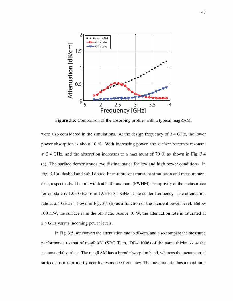
43
1.5 2 2.5 3 3.5 40
0.5
1
1.5
2
Frequency [GHz]
Att
en
ua
tio
n [
dB
/cm
]
1.5 2 2.5 3 3.5 40
0.5
1
1.5
2
Frequency [GHz]
Att
en
ua
tio
n [
dB
/cm
]
magRAM
On state
O! state
Figure 3.5: Comparison of the absorbing profiles with a typical magRAM.
were also considered in the simulations. At the design frequency of 2.4 GHz, the lower
power absorption is about 10 %. With increasing power, the surface becomes resonant
at 2.4 GHz, and the absorption increases to a maximum of 70 % as shown in Fig. 3.4
(a). The surface demonstrates two distinct states for low and high power conditions. In
Fig. 3.4(a) dashed and solid dotted lines represent transient simulation and measurement
data, respectively. The full width at half maximum (FWHM) absorptivity of the metasurface
for on-state is 1.05 GHz from 1.95 to 3.1 GHz at the center frequency. The attenuation
rate at 2.4 GHz is shown in Fig. 3.4 (b) as a function of the incident power level. Below
100 mW, the surface is in the off-state. Above 10 W, the attenuation rate is saturated at
2.4 GHz versus incoming power levels.
In Fig. 3.5, we convert the attenuation rate to dB/cm, and also compare the measured
performance to that of magRAM (SRC Tech. DD-11006) of the same thickness as the
metamaterial surface. The magRAM has a broad absorption band, whereas the metamaterial
surface absorbs primarily near its resonance frequency. The metamaterial has a maximum

44
absorption rate that is approximately equal to that of the magRAM in the waveguide
measurement. However, it performs better in measurements of surface waves on open
surfaces, as discussed in the next sections.
3.3.2 Surface Wave Measurement
Figure 3.6: Measurement setup for surface field suppression.
To study the effect of surface waves in an open environment, we constructed a large
area of the nonlinear metasurface, measuring 391 mm by 527 mm, and 23 x 31 unit cells.
The measurement environment is shown in Fig. 3.6. Fig. 3.7 shows the geometry of the
measurement, as well as low and high power field plots for the nonlinear metasurface. We
also measured the field profile on standard magnetic radar absorbing material, magRAM
(SRC Tech. DD-11006) of the same thickness. We excited surface waves by launching them
from an open-ended waveguide placed adjacent to one edge of the surface. The measurement
45
setup with planar near field scanner, network analyzer (Agilent E5071C), and amplifier. A
wave is launched near the center left edge of the surface. The surface was placed in our
near-field scanner, which consists of two linear position controllers arranged to provide x-y
scanning over a 1 square meter area shown in Fig. 3.7 (b).
We scanned a small coaxial probe over an area 2 mm above the surface to measure
the electric field as a function of position for various power levels shown in Fig. 3.7 (c)-(f).
The power levels of each figure are in Fig. 3.7 (c) metasurface at 4.8 mW, Fig. 3.7 (d)
metasurface at 34 W, Fig. 3.7 (e) magRAM at 4.8 mW, and Fig. 3.7 (f) magRAM at 34 W,
respectively. The waveguide excites a surface wave that spreads out over the surface, and
is also attenuated by losses in the surface. As the power level is increased, the nonlinear
metasurface shows increasing absorption, seen as reduced relative field strength from Fig. 3.7
(c) to Fig. 3.7 (d). A transition to the highly absorbing state occurs at approximately 10 W
of input power, although the two plots represent two extremes of a continuous variation in
absorption. The magRAM shows the same field profile for low and high field strength in
Fig. 3.7 (e) and Fig. 3.7 (f), respectively. This is expected because it is a linear absorber.
Unfortunately, it was not possible to extract the attenuation rate from these data because
the reduction in field strength occurs due to both diffraction from the source, and also
attenuation, with different regions of the surface having different attenuation rates. The
surface field transitions of the metasurface and magRAM under off- and on-states depending
on the input powers are shown in Fig. 3.8, 3.9, 3.10, and 3.11, respectively.
3.3.3 Leakage Field Measurement
In order to demonstrate the use of our nonlinear metasurface in a practical application,
we constructed a metallic box with a narrow opening shown in Fig. 3.12 (a). This would
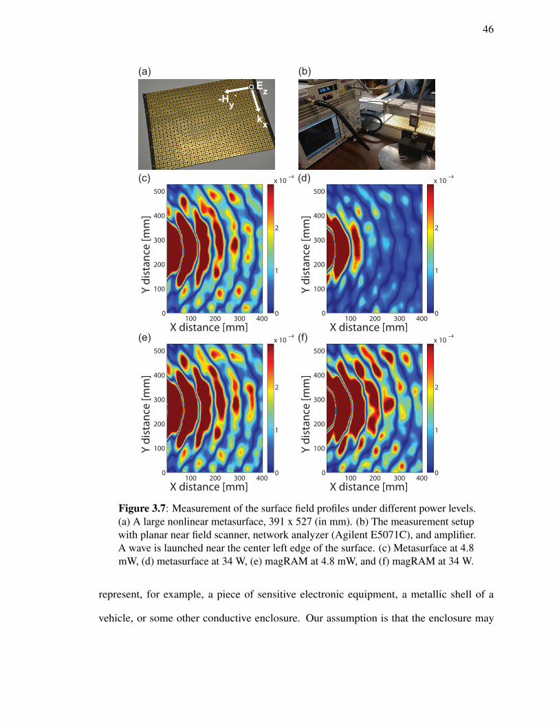
46
X distance [mm]
Y d
ista
nc
e [
mm
]
100 200 300 400
500
400
300
200
100
0 0
1
2
x 10−4
X distance [mm]
Y d
ista
nc
e [
mm
]
100 200 300 400
500
400
300
200
100
0 0
1
2
x 10−4
X distance [mm]
Y d
ista
nc
e [
mm
]
100 200 300 400
500
400
300
200
100
0 0
1
2
x 10−4
X distance [mm]
Y d
ista
nc
e [
mm
]
100 200 300 400
500
400
300
200
100
0 0
1
2
x 10−4
(a)
(c) (d)
(e) (f)
(b)
Ez
-Hy`
kx
Figure 3.7: Measurement of the surface field profiles under different power levels.(a) A large nonlinear metasurface, 391 x 527 (in mm). (b) The measurement setupwith planar near field scanner, network analyzer (Agilent E5071C), and amplifier.A wave is launched near the center left edge of the surface. (c) Metasurface at 4.8mW, (d) metasurface at 34 W, (e) magRAM at 4.8 mW, and (f) magRAM at 34 W.
represent, for example, a piece of sensitive electronic equipment, a metallic shell of a
vehicle, or some other conductive enclosure. Our assumption is that the enclosure may

47
DUT
P6.7
9903
1dBm
(4.8
mW
)
5010
015
020
025
030
035
0
50 100
150
200
250
300
350
400
450
500
012x 10
-4DU
T P7
.807
478d
Bm (6
mW
)
5010
015
020
025
030
035
0
50 100
150
200
250
300
350
400
450
500
012x 10
-4DU
T P8
.813
712d
Bm (7
.6m
W)
5010
015
020
025
030
035
0
50 100
150
200
250
300
350
400
450
500
012x 10
-4DU
T P9
.811
666d
Bm (9
.6m
W)
5010
015
020
025
030
035
0
50 100
150
200
250
300
350
400
450
500
012x 10
-4DU
T P1
0.82
4895
dBm
(12.
1mW
)
5010
015
020
025
030
035
0
50 100
150
200
250
300
350
400
450
500
012x 10
-4DU
T P1
1.83
4126
dBm
(15.
3mW
)
5010
015
020
025
030
035
0
50 100
150
200
250
300
350
400
450
500
012x 10
-4DU
T P1
2.83
3897
dBm
(19.
2mW
)
5010
015
020
025
030
035
0
50 100
150
200
250
300
350
400
450
500
012x 10
-4
DUT
P13.
8427
95dB
m (2
4.2m
W)
5010
015
020
025
030
035
0
50 100
150
200
250
300
350
400
450
500
012x 10
-4DU
T P1
4.85
1528
dBm
(30.
6mW
)
5010
015
020
025
030
035
0
50 100
150
200
250
300
350
400
450
500
012x 10
-4DU
T P1
5.85
294d
Bm (3
8.5m
W)
5010
015
020
025
030
035
0
50 100
150
200
250
300
350
400
450
500
012x 10
-4DU
T P1
6.86
0104
dBm
(48.
5mW
)
5010
015
020
025
030
035
0
50 100
150
200
250
300
350
400
450
500
012x 10
-4DU
T P1
7.85
9761
dBm
(61.
1mW
)
5010
015
020
025
030
035
0
50 100
150
200
250
300
350
400
450
500
012x 10
-4DU
T P1
8.84
8742
dBm
(76.
7mW
)
5010
015
020
025
030
035
0
50 100
150
200
250
300
350
400
450
500
012x 10
-4DU
T P1
9.82
7681
dBm
(96.
1mW
)
5010
015
020
025
030
035
0
50 100
150
200
250
300
350
400
450
500
012x 10
-4
DUT
P20.
8004
15dB
m (0
.12W
)
5010
015
020
025
030
035
0
50 100
150
200
250
300
350
400
450
500
012x 10
-4DU
T P2
1.75
1019
dBm
(0.1
5W)
5010
015
020
025
030
035
0
50 100
150
200
250
300
350
400
450
500
012x 10
-4DU
T P2
2.66
6784
dBm
(0.1
8W)
5010
015
020
025
030
035
0
50 100
150
200
250
300
350
400
450
500
012x 10
-4DU
T P2
3.55
437d
Bm (0
.23W
)
5010
015
020
025
030
035
0
50 100
150
200
250
300
350
400
450
500
012x 10
-4DU
T P2
4.38
6635
dBm
(0.2
7W)
5010
015
020
025
030
035
0
50 100
150
200
250
300
350
400
450
500
012x 10
-4DU
T P2
5.16
2104
dBm
(0.3
3W)
5010
015
020
025
030
035
0
50 100
150
200
250
300
350
400
450
500
012x 10
-4DU
T P2
5.89
0606
dBm
(0.3
9W)
5010
015
020
025
030
035
0
50 100
150
200
250
300
350
400
450
500
012x 10
-4
Figure 3.8: Off-State surface field profiles of the metasurface
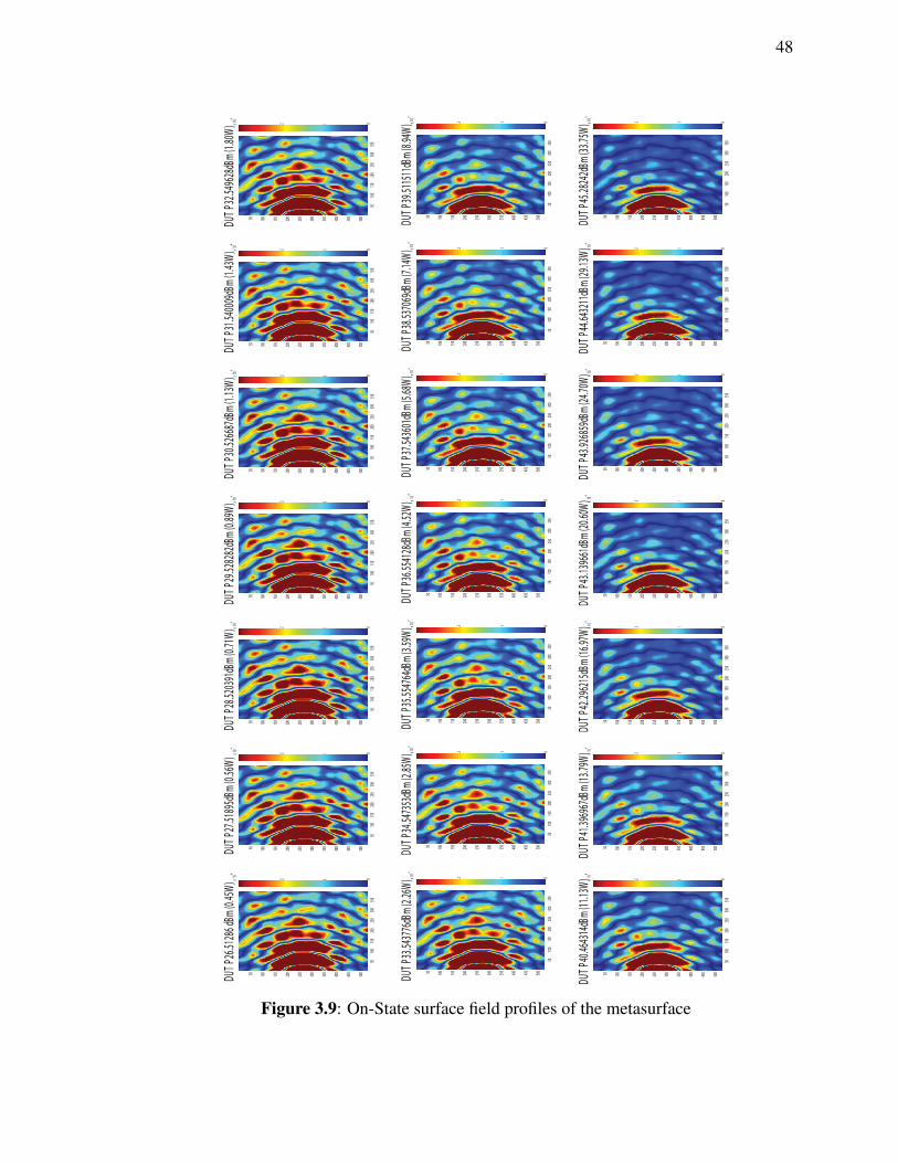
48
DUT
P26.
5128
6 dB
m (0
.45W
)
5010
015
020
025
030
035
0
50 100
150
200
250
300
350
400
450
500
012x 10
-4DU
T P2
7.51
895d
Bm (0
.56W
)
5010
015
020
025
030
035
0
50 100
150
200
250
300
350
400
450
500
012x 10
-4DU
T P2
8.52
0391
dBm
(0.7
1W)
5010
015
020
025
030
035
0
50 100
150
200
250
300
350
400
450
500
012x 10
-4DU
T P2
9.52
8282
dBm
(0.8
9W)
5010
015
020
025
030
035
0
50 100
150
200
250
300
350
400
450
500
012x 10
-4DU
T P3
0.52
6687
dBm
(1.1
3W)
5010
015
020
025
030
035
0
50 100
150
200
250
300
350
400
450
500
012x 10
-4DU
T P3
1.54
0009
dBm
(1.4
3W)
5010
015
020
025
030
035
0
50 100
150
200
250
300
350
400
450
500
012x 10
-4DU
T P3
2.54
9628
dBm
(1.8
0W)
5010
015
020
025
030
035
0
50 100
150
200
250
300
350
400
450
500
012x 10
-4
DUT
P33.
5437
76dB
m (2
.26W
)
5010
015
020
025
030
035
0
50 100
150
200
250
300
350
400
450
500
012x 10
-4DU
T P3
4.54
7353
dBm
(2.8
5W)
5010
015
020
025
030
035
0
50 100
150
200
250
300
350
400
450
500
012x 10
-4DU
T P3
5.55
4764
dBm
(3.5
9W)
5010
015
020
025
030
035
0
50 100
150
200
250
300
350
400
450
500
012x 10
-4DU
T P3
6.55
4128
dBm
(4.5
2W)
5010
015
020
025
030
035
0
50 100
150
200
250
300
350
400
450
500
012x 10
-4DU
T P3
7.54
3601
dBm
(5.6
8W)
5010
015
020
025
030
035
0
50 100
150
200
250
300
350
400
450
500
012x 10
-4DU
T P3
8.53
7069
dBm
(7.1
4W)
5010
015
020
025
030
035
0
50 100
150
200
250
300
350
400
450
500
012x 10
-4DU
T P3
9.51
1511
dBm
(8.9
4W)
5010
015
020
025
030
035
0
50 100
150
200
250
300
350
400
450
500
012x 10
-4
DUT
P40.
4643
14dB
m (1
1.13
W)
5010
015
020
025
030
035
0
50 100
150
200
250
300
350
400
450
500
012x 10
-4DU
T P4
1.39
6967
dBm
(13.
79W
)
5010
015
020
025
030
035
0
50 100
150
200
250
300
350
400
450
500
012x 10
-4DU
T P4
2.29
6215
dBm
(16.
97W
)
5010
015
020
025
030
035
0
50 100
150
200
250
300
350
400
450
500
012x 10
-4DU
T P4
3.13
9661
dBm
(20.
60W
)
5010
015
020
025
030
035
0
50 100
150
200
250
300
350
400
450
500
012x 10
-4DU
T P4
3.92
6859
dBm
(24.
70W
)
5010
015
020
025
030
035
0
50 100
150
200
250
300
350
400
450
500
012x 10
-4DU
T P4
4.64
3211
dBm
(29.
13W
)
5010
015
020
025
030
035
0
50 100
150
200
250
300
350
400
450
500
012x 10
-4DU
T P4
5.28
242d
Bm (3
3.75
W)
5010
015
020
025
030
035
0
50 100
150
200
250
300
350
400
450
500
012x 10
-4
Figure 3.9: On-State surface field profiles of the metasurface

49
DUT
P6.7
9903
1dBm
(4.8
mW
)
5010
015
020
025
030
035
0
50 100
150
200
250
300
350
400
450
500
012x 10
-4DU
T P7
.807
478d
Bm (6
mW
)
5010
015
020
025
030
035
0
50 100
150
200
250
300
350
400
450
500
012x 10
-4DU
T P8
.813
712d
Bm (7
.6m
W)
5010
015
020
025
030
035
0
50 100
150
200
250
300
350
400
450
500
012x 10
-4DU
T P9
.811
666d
Bm (9
.6m
W)
5010
015
020
025
030
035
0
50 100
150
200
250
300
350
400
450
500
012x 10
-4DU
T P1
0.82
4895
dBm
(12.
1mW
)
5010
015
020
025
030
035
0
50 100
150
200
250
300
350
400
450
500
012x 10
-4DU
T P1
1.83
4126
dBm
(15.
3mW
)
5010
015
020
025
030
035
0
50 100
150
200
250
300
350
400
450
500
012x 10
-4DU
T P1
2.83
3897
dBm
(19.
2mW
)
5010
015
020
025
030
035
0
50 100
150
200
250
300
350
400
450
500
012x 10
-4
DUT
P13.
8427
95dB
m (2
4.2m
W)
5010
015
020
025
030
035
0
50 100
150
200
250
300
350
400
450
500
012x 10
-4DU
T P1
4.85
1528
dBm
(30.
6mW
)
5010
015
020
025
030
035
0
50 100
150
200
250
300
350
400
450
500
012x 10
-4DU
T P1
5.85
294d
Bm (3
8.5m
W)
5010
015
020
025
030
035
0
50 100
150
200
250
300
350
400
450
500
012x 10
-4DU
T P1
6.86
0104
dBm
(48.
5mW
)
5010
015
020
025
030
035
0
50 100
150
200
250
300
350
400
450
500
012x 10
-4DU
T P1
7.85
9761
dBm
(61.
1mW
)
5010
015
020
025
030
035
0
50 100
150
200
250
300
350
400
450
500
012x 10
-4DU
T P1
8.84
8742
dBm
(76.
7mW
)
5010
015
020
025
030
035
0
50 100
150
200
250
300
350
400
450
500
012x 10
-4DU
T P1
9.82
7681
dBm
(96.
1mW
)
5010
015
020
025
030
035
0
50 100
150
200
250
300
350
400
450
500
012x 10
-4
DUT
P20.
8004
15dB
m (0
.12W
)
5010
015
020
025
030
035
0
50 100
150
200
250
300
350
400
450
500
012x 10
-4DU
T P2
1.75
1019
dBm
(0.1
5W)
5010
015
020
025
030
035
0
50 100
150
200
250
300
350
400
450
500
012x 10
-4DU
T P2
2.66
6784
dBm
(0.1
8W)
5010
015
020
025
030
035
0
50 100
150
200
250
300
350
400
450
500
012x 10
-4DU
T P2
3.55
437d
Bm (0
.23W
)
5010
015
020
025
030
035
0
50 100
150
200
250
300
350
400
450
500
012x 10
-4DU
T P2
4.38
6635
dBm
(0.2
7W)
5010
015
020
025
030
035
0
50 100
150
200
250
300
350
400
450
500
012x 10
-4DU
T P2
5.16
2104
dBm
(0.3
3W)
5010
015
020
025
030
035
0
50 100
150
200
250
300
350
400
450
500
012x 10
-4DU
T P2
5.89
0606
dBm
(0.3
9W)
5010
015
020
025
030
035
0
50 100
150
200
250
300
350
400
450
500
012x 10
-4
Figure 3.10: Off-State surface field profiles of the magRAM

50
DUT
P26.
5128
6 dB
m (0
.45W
)
5010
015
020
025
030
035
0
50 100
150
200
250
300
350
400
450
500
012x 10
-4DU
T P2
7.51
895d
Bm (0
.56W
)
5010
015
020
025
030
035
0
50 100
150
200
250
300
350
400
450
500
012x 10
-4DU
T P2
8.52
0391
dBm
(0.7
1W)
5010
015
020
025
030
035
0
50 100
150
200
250
300
350
400
450
500
012x 10
-4DU
T P2
9.52
8282
dBm
(0.8
9W)
5010
015
020
025
030
035
0
50 100
150
200
250
300
350
400
450
500
012x 10
-4DU
T P3
0.52
6687
dBm
(1.1
3W)
5010
015
020
025
030
035
0
50 100
150
200
250
300
350
400
450
500
012x 10
-4DU
T P3
1.54
0009
dBm
(1.4
3W)
5010
015
020
025
030
035
0
50 100
150
200
250
300
350
400
450
500
012x 10
-4DU
T P3
2.54
9628
dBm
(1.8
0W)
5010
015
020
025
030
035
0
50 100
150
200
250
300
350
400
450
500
012x 10
-4
DUT
P33.
5437
76dB
m (2
.26W
)
5010
015
020
025
030
035
0
50 100
150
200
250
300
350
400
450
500
012x 10
-4DU
T P3
4.54
7353
dBm
(2.8
5W)
5010
015
020
025
030
035
0
50 100
150
200
250
300
350
400
450
500
012x 10
-4DU
T P3
5.55
4764
dBm
(3.5
9W)
5010
015
020
025
030
035
0
50 100
150
200
250
300
350
400
450
500
012x 10
-4DU
T P3
6.55
4128
dBm
(4.5
2W)
5010
015
020
025
030
035
0
50 100
150
200
250
300
350
400
450
500
012x 10
-4DU
T P3
7.54
3601
dBm
(5.6
8W)
5010
015
020
025
030
035
0
50 100
150
200
250
300
350
400
450
500
012x 10
-4DU
T P3
8.53
7069
dBm
(7.1
4W)
5010
015
020
025
030
035
0
50 100
150
200
250
300
350
400
450
500
012x 10
-4DU
T P3
9.51
1511
dBm
(8.9
4W)
5010
015
020
025
030
035
0
50 100
150
200
250
300
350
400
450
500
012x 10
-4
DUT
P40.
4643
14dB
m (1
1.13
W)
5010
015
020
025
030
035
0
50 100
150
200
250
300
350
400
450
500
012x 10
-4DU
T P4
1.39
6967
dBm
(13.
79W
)
5010
015
020
025
030
035
0
50 100
150
200
250
300
350
400
450
500
012x 10
-4DU
T P4
2.29
6215
dBm
(16.
97W
)
5010
015
020
025
030
035
0
50 100
150
200
250
300
350
400
450
500
012x 10
-4DU
T P4
3.13
9661
dBm
(20.
60W
)
5010
015
020
025
030
035
0
50 100
150
200
250
300
350
400
450
500
012x 10
-4DU
T P4
3.92
6859
dBm
(24.
70W
)
5010
015
020
025
030
035
0
50 100
150
200
250
300
350
400
450
500
012x 10
-4DU
T P4
4.64
3211
dBm
(29.
13W
)
5010
015
020
025
030
035
0
50 100
150
200
250
300
350
400
450
500
012x 10
-4DU
T P4
5.28
242d
Bm (3
3.75
W)
5010
015
020
025
030
035
0
50 100
150
200
250
300
350
400
450
500
012x 10
-4
Figure 3.11: On-State surface field profiles of the magRAM
51
not be perfectly sealed, and external fields can leak in through small gaps, seams, or other
openings. By covering the area around the gaps with a nonlinear absorber, one can limit
the field level that is allowed to penetrate the box. For the following experiments, the box
measured 560 x 910 x 100 (in mm), and a 9 mm wide opening was located on one face.
We developed an experimental approach to measure the field leakage into the enclosure
through the narrow opening and determined the effect of the nonlinear metasurface coating
compared to a conventional magRAM coating as well as a bare metal surface. The metal
box was placed in an anechoic chamber, and illuminated by 2.4 GHz waves from a horn
antenna located on one wall of the chamber, 2.5 m away from the box as shown in Fig. 3.12
(b). The signals from the network analyzer were amplified to as much as 150 W by a high
power amplifier (Ophir 5265) and they impinged upon the box at a grazing angle relative to
the face which contained the opening. The waves were vertically polarized relative to the
top surface, and propagated perpendicular to the gap in that surface. We used this geometry
in order to efficiently excite transverse magnetic surface waves which could penetrate the
gap.
We placed a small electric field probe inside the box below the opening, and measured
the field strength inside the box for various surface coatings. The field probe was calibrated
by placing it at the same location without the box, and using the Friis transmission equation.
The field level inside the box is shown in Fig. 3.12 (c) as a function of the impinging field
strength for the nonlinear metasurface coating, compared to the conventional magRAM
coating, and to the bare metal surface. For both the metal surface and the magRAM, the
field strength inside the box is a linear function of the external field strength, as expected
because these are both linear materials. The magRAM shows a reduction in internal field
strength relative to the bare metal case because of its absorption. However, the metasurface
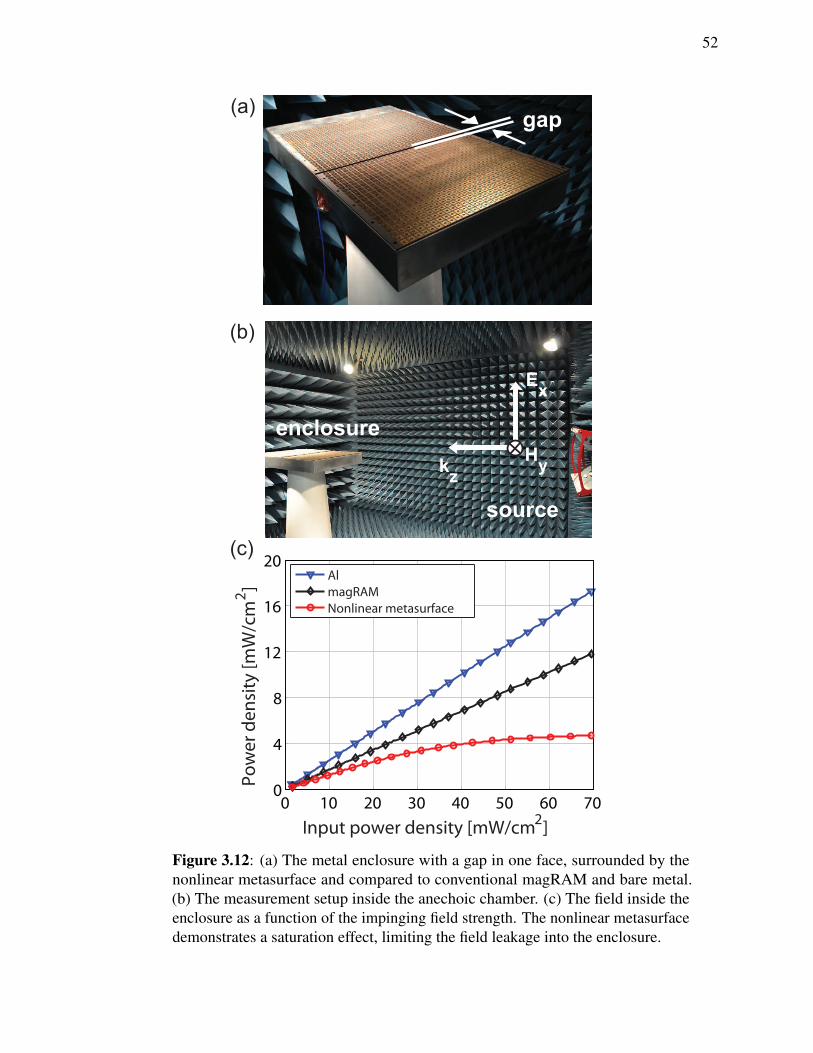
52
gap
0 10 20 30 40 50 60 700
4
8
12
16
20
Input power density [mW/cm2
]
Po
we
r d
en
sity
[m
W/c
m2
]
Al
magRAM
Nonlinear metasurface
(b)
(a)
source
enclosure
(c)
Ex
Hyk
z
Figure 3.12: (a) The metal enclosure with a gap in one face, surrounded by thenonlinear metasurface and compared to conventional magRAM and bare metal.(b) The measurement setup inside the anechoic chamber. (c) The field inside theenclosure as a function of the impinging field strength. The nonlinear metasurfacedemonstrates a saturation effect, limiting the field leakage into the enclosure.
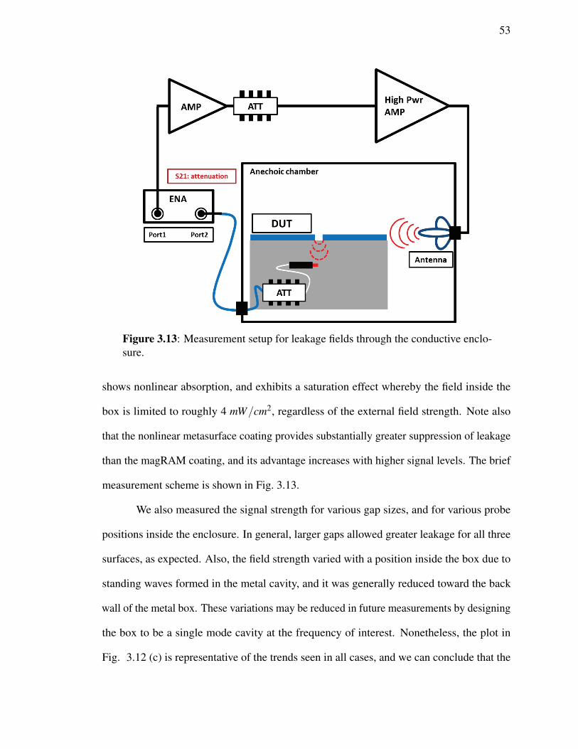
53
Figure 3.13: Measurement setup for leakage fields through the conductive enclo-sure.
shows nonlinear absorption, and exhibits a saturation effect whereby the field inside the
box is limited to roughly 4 mW/cm2, regardless of the external field strength. Note also
that the nonlinear metasurface coating provides substantially greater suppression of leakage
than the magRAM coating, and its advantage increases with higher signal levels. The brief
measurement scheme is shown in Fig. 3.13.
We also measured the signal strength for various gap sizes, and for various probe
positions inside the enclosure. In general, larger gaps allowed greater leakage for all three
surfaces, as expected. Also, the field strength varied with a position inside the box due to
standing waves formed in the metal cavity, and it was generally reduced toward the back
wall of the metal box. These variations may be reduced in future measurements by designing
the box to be a single mode cavity at the frequency of interest. Nonetheless, the plot in
Fig. 3.12 (c) is representative of the trends seen in all cases, and we can conclude that the

54
nonlinear metasurface coating provides not only an absorption advantage at its resonant
frequency relative to a conventional magRAM, but also a nonlinear saturation effect, limiting
the field penetration through a gap in a metal enclosure.
3.4 Conclusion
In this chapter, we have demonstrated a kind of nonlinear metasurface coating that
changes its conductive topology in response to the power of the incoming wave. It converts
from behaving as a simple capacitive sheet over a ground plane into a high impedance surface
when the signal level surpasses the turn-on voltage of diodes at the vertical vias, and they
become conductive. Resistors between the patches provide substantial absorption near the
LC resonance frequency, which may be set by the appropriate choice of the patch shape and
substrate thickness. We have designed the surface to provide a significant absorption contrast
at 2.4 GHz, and have demonstrated a change from 10 % to 70 % absorption with increasing
power level, for small samples inside waveguides. Furthermore, we have performed planar
near-field scans on electrically large surfaces. We have shown that at high power levels,
the nonlinear metasurface can provide greater attenuation than a conventional magRAM
coating near its design frequency. We have also shown that it can limit the amount of
electromagnetic leakage through a gap in a metal enclosure, demonstrating that it can be
used for practical applications.
Chapter 3 is based on and is mostly a reprint of the following papers: S. Kim, H.
Wakatsuchi, J. Rushton, D. Sievenpiper, ”Switchable Nonlinear Metasurfaces for Absorbing
High Power Surface Waves”, Applied Physics Letters 108, 041903, 2016.; S. Kim, H.
Wakatsuchi, J. Rushton, D. Sievenpiper, ”Nonlinear Metamaterial Surfaces for Absorption
of High Power Microwave Surface Currents”, IEEE Antennas and Propagation Symposium

55
Digest, Orlando, FL, USA, July 8-14, 2013. The dissertation author was the primary author
of the work in this chapter, and the co-authors have approved the use of the material for this
dissertation.

Chapter 4
Self-Tuning Metamaterial Surfaces
Conventional absorbers of resonance type offer various implementations due to their
thin and lightweight characteristics. There is, however, a fundamental relationship between
the electrical thickness of the absorbing materials or structures and their absorption capability.
Thus, compatibility between the thinner absorber and the broader absorbing properties is not
easily available by linear and passive methods, even though the instantaneous bandwidth
is still limited. In this chapter, a new concept of an electromagnetic absorber has been
addressed with a nonlinear and active feedback circuit, and eventually gives a broadband
tunability, which is greater than the instantaneous bandwidth for any of the individual tuning
frequencies.
4.1 Concept and Mechanism
4.1.1 Background and Motivation
In general, reactive surfaces used as a resonant absorber have limitations in their
narrow bandwidth, which is determined by the relationship between the bandwidth and the
56

57
thickness. Thus, it is not available from a wide bandwidth absorbing structure, which has a
relatively thin thickness, even metamaterial, or matasurface absorbers, which was discussed
in previous chapters. For an instant, the bandwidth of the conventional high impedance
surface has been determined by a thickness of the dielectric substrate.
B =2πµrt
λ0(4.1)
Here, the µr is the relative permeability of the substrate, λ0 is the wavelength of the
center frequency at the electromagnetic band gap (EBG) of the high impedance surface,
and t is the thickness of the substrate. For example, a reactive coating surface built for 1-2
GHz range has around 4% of bandwidth. There are several approaches to achieve broad
bandwidth performances in applying a multi-resonant structure such as a different size
of unit cells or multilayers with different unit cell geometry. As with other methods, the
Q-factor can be manipulated by adding a loss ( 4.2) to the lower Q-value for the broader
bandwidth. Nevertheless, the linear and passive techniques to achieve the wide bandwidth
have restricted its use in practical implementations.
Q =XR=
BG
=Engergystored
Energydissipated(4.2)
Metamaterials with nonlinear circuit components can give an additional degree of
freedom to help manipulate unique characteristics in the limitation of linear approaches. The
unit cells constructed in metamaterials display a periodic array on a sub-wavelength scale,
and behave like an electrically effective medium, including effective permittivity εe f f and
permeability µe f f , which properties can be determined by the deployed nonlinear circuits.
To achieve a broad bandwidth over the linear limitation, we suggest a novel concept of

58
nonlinear active metamaterial surfaces.
4.1.2 Mechanisms for Self-Tuning Metasurfaces
Figure 4.1: Mechanism diagram for the self-tuning metasurface
The main mechanism of the self-tuning metasurface is basically based on the tuning
methods. In general, metamaterials are passive and linear mediums with fixed resonant
frequencies. Thus, the tunability of the metamaterials is conducted by populated circuit
components and external devices in order to tune the resonant frequencies. Previously, the
tunable mechanism works are carried out by diodes electrically [50, 51, 52], MEMS devices
mechanically [53], and transistors [54]. In particular, the electrical tuning methods by diodes
required external DC bias to transit the impedance of the diodes. Most of the tuning systems
needed an external source, extra controller, computer-based tracking systems, and manual
calibration. Additionally, the tuning system is independent of the incident signals.

59
Figure 4.2: Scheme of the co-simulation
Here, the proposed active metasurface induces a unique tuning system, which results
in adaptive tunability that depends on incoming frequencies. In other words, the tunable
metasurface is able to sense a frequency of an incident signal, and then alters to match
the frequency, called self-tuning. To achieve this newly tuned mechanism, the self-tuning
metasurface involved two states: sensing and responding parts as shown in Fig. 4.1. The
responding part was constructed from the high impedance surface and varactor diodes
embedded in the gap between the periodic metallic patches on the metasurface. The sensing
part was basically based on an RF-DC rectifier, which consists of a slope detector and a
diode rectifier circuit to generate DC voltages to assign bias to varactors on the responding
part.

60
Figure 4.3: Overall scheme of the self-tuning circuit board.
To verify the rectified DC voltage, we carried out a co-simulation of full wave
EM simulation and circuit analysis under a time transient as shown in Fig. 4.2. In the
co-simulation, transient voltage data are checked at four steps: A© represents input RF
signals at 3 GHz with 1 W as a source power to the metasurface in the normal direction
of incoming waves, B© represents sensing voltages after the sensing unit cell, C© shows
rectified DC voltages through the self-tuning circuit, and D© exhibits the amplified DC bias
with the gain of 10 and DC offset of 1 V from the rectified voltages at the output of the
self-tuning circuit board. Therefore, we verified total co-simulation can generate a proper
DC bias to tune the varactors on the surface for the nonlinear active metasurface.
61
4.2 Self-Tuning Circuit Board
The overall scheme of the self-tuning circuit board is shown in Fig. 4.3. The
designed circuit board has a broadband frequency response from 1 to 4 GHz. The circuit
board has consisted of an LNA to amplify input powers, a limiter to only depend on incoming
frequencies, a Z-matching network for broadband frequencies, slope detector to response
input frequencies, DC pass filter for the generated DC, and op-amps to match the desired
control bias to the varactors on the self-tuning metasurface. The input and output ports are
matched to 50Ω. The input port is directly connected to the sensing cell of the metasurface.
The LNA is used to amplify input signals through the sensing cell on the metasurface. The
efficiency of the RF-DC rectification is determined by input powers toward to the rectifying
diode.
ηRF−DC =PDC
PRF=
V 2DC/RL
PRF(4.3)
Here, V 2DC represents the rectified DC voltages at the output, RL, which represents a load
resistance, 700kΩ, and PRF , which represents an input power to the rectifying diode. A RF
limiter is used to assign stable input powers to the diode for an interesting frequency band.
The characteristic impedance is 50Ω, and the input impedance of the diode is (67.4+ j9.2)Ω.
Thus, impedance matching network is applied to transfer between the different impedances
to avoid impedance mismatch. The slope detector is designed with a lumped LC component
in a parallel connection and a rectifying diode. After the slope detector, three cascade radial
stubs were used as RF harmonic filters. The rectified DC voltages are required to match the
desired DC bias to control the varactor diodes in the responding part.
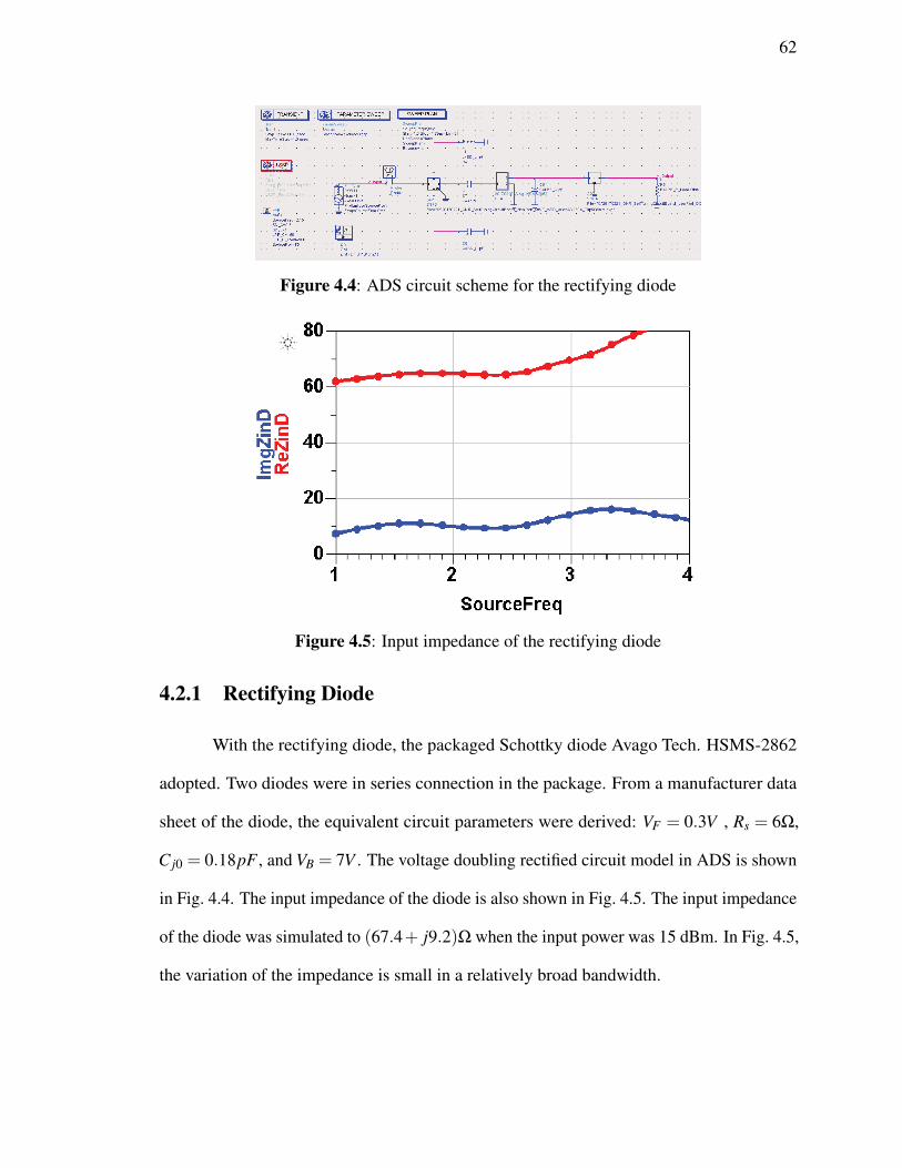
62
Figure 4.4: ADS circuit scheme for the rectifying diode
Figure 4.5: Input impedance of the rectifying diode
4.2.1 Rectifying Diode
With the rectifying diode, the packaged Schottky diode Avago Tech. HSMS-2862
adopted. Two diodes were in series connection in the package. From a manufacturer data
sheet of the diode, the equivalent circuit parameters were derived: VF = 0.3V , Rs = 6Ω,
C j0 = 0.18pF , and VB = 7V . The voltage doubling rectified circuit model in ADS is shown
in Fig. 4.4. The input impedance of the diode is also shown in Fig. 4.5. The input impedance
of the diode was simulated to (67.4+ j9.2)Ω when the input power was 15 dBm. In Fig. 4.5,
the variation of the impedance is small in a relatively broad bandwidth.

63
Figure 4.6: Model and simulation data of impedance matching network
4.2.2 Impedance Matching Network
The rectifying circuit had an impedance mismatch between input impedance and the
input diode impedance, so three cascaded sections of a quarter wavelength transformer were
used, which helped to enhance the bandwidth. The impedance for broadband frequencies
was properly matched as shown in Fig. 4.6.
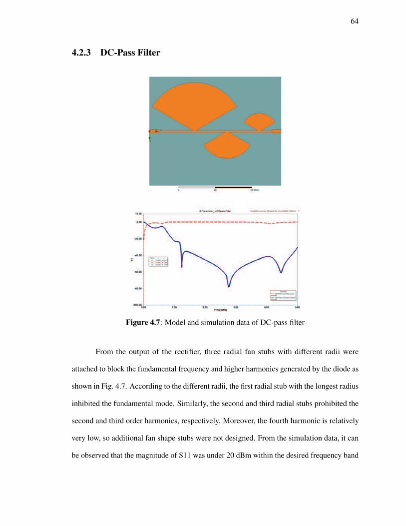
64
4.2.3 DC-Pass Filter
Figure 4.7: Model and simulation data of DC-pass filter
From the output of the rectifier, three radial fan stubs with different radii were
attached to block the fundamental frequency and higher harmonics generated by the diode as
shown in Fig. 4.7. According to the different radii, the first radial stub with the longest radius
inhibited the fundamental mode. Similarly, the second and third radial stubs prohibited the
second and third order harmonics, respectively. Moreover, the fourth harmonic is relatively
very low, so additional fan shape stubs were not designed. From the simulation data, it can
be observed that the magnitude of S11 was under 20 dBm within the desired frequency band

65
Figure 4.8: Fabricated sample of the self-tuning metasurface
from the fundamental, 2.45 GHz, to the third order harmonic, 7.35 GHz. Therefore, the
radial stubs effectively suppressed the fundamental and higher harmonic modes.
4.3 Responding Part of Self-Tuning Metasurface
The self-tuning metasurface was planned to fabricate with the optimized sensing
cell. The built metasurface was 25 x 40 cm with three Cu cladding layers including two
dielectric layers. The top surface is shown in Fig. 4.8, and each unit cell has a 10 mm as
period and a 1.4 mm as the gap distance. The first dielectric material is RO5880 with a
1.575 mm thickness, and the second one was on FR4 for the circuits, such as buffers and
resistors, to protect the varactors. On the bottom surface, a physical hole is used to deploy a
SMA connector to receive incoming powers through the sensing unit cell.
4.4 Measurement and Results
The closed-loop measurement setup under a high power system as shown in Fig. 4.9.
In Fig. 4.9, the measurement setup is constructed with a VNA, two antennas, a self-tuning

66
Figure 4.9: Scheme of the measurement setup
metasurface, a self-tuning circuit board, and DC suppliers to the op-amps of the circuit
board. The first and second antennas were used as a transceiver (Tx) and a receiver (Rx),
and placed away from the metasurface, 1 ft and 11 inches, respectively. Also, the angle
between the two antennas was 20 degrees. The measurement scheme of the closed loop
system is shown in Fig. 4.10. From the sensing cell of the metasurface, the input signals
were amplified by the LNAs because the input signals were too low to activate the rectifier
circuits on the self-tuning circuit board. The diode, which was used on the self-tuning
circuit to show the stable rectifier performance under 15 dBm input power, also showed
stable inputs in the self-tuning board will generate stable rectified DC voltages to tune
the metasurface. The measurement data from the absorption under the high power closed
loop system is shown in Fig. 4.11. The input power to the metasurface was 30 dBm, and
frequencies were swept from 2 to 4 GHz. The thin solid lines represent a linear absorption
while applying the DC bias from 1 to 14 volts to the metasurface directly. The blue dotted
line represents a nonlinear absorption from the closed loop measurement, and the absorption
band that appeared from 2.2 to 3.2 GHz. Some of the points showed unstable absorptivity
because of the fluctuation input powers in the self-tuning circuit board. The unstable input
powers were from the near-field effect between the source antenna and the metasurface. To
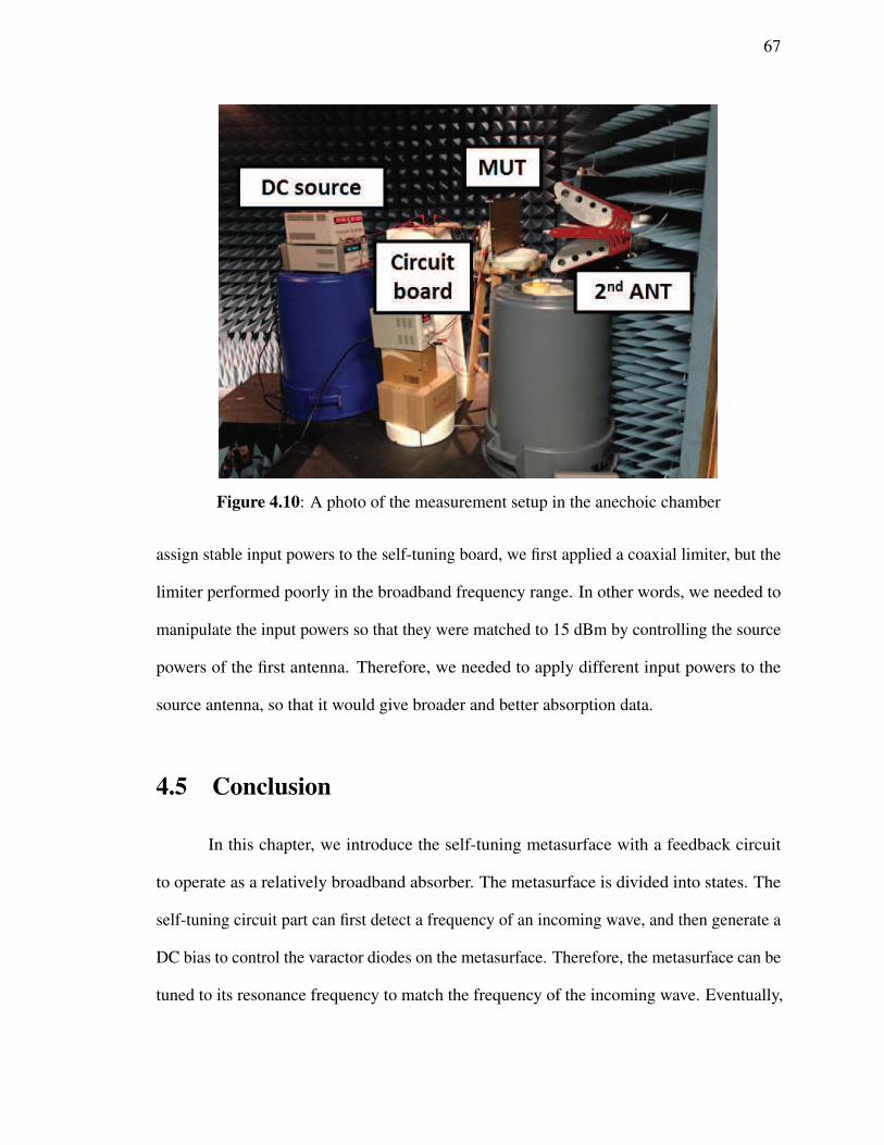
67
Figure 4.10: A photo of the measurement setup in the anechoic chamber
assign stable input powers to the self-tuning board, we first applied a coaxial limiter, but the
limiter performed poorly in the broadband frequency range. In other words, we needed to
manipulate the input powers so that they were matched to 15 dBm by controlling the source
powers of the first antenna. Therefore, we needed to apply different input powers to the
source antenna, so that it would give broader and better absorption data.
4.5 Conclusion
In this chapter, we introduce the self-tuning metasurface with a feedback circuit
to operate as a relatively broadband absorber. The metasurface is divided into states. The
self-tuning circuit part can first detect a frequency of an incoming wave, and then generate a
DC bias to control the varactor diodes on the metasurface. Therefore, the metasurface can be
tuned to its resonance frequency to match the frequency of the incoming wave. Eventually,

68
Figure 4.11: Measurement data from the self-tuning metasurface
the tunable range of the metasurface can be extended over the limitation of the linear and
passive metasurfaces.
Chapter 4 is based on and is mostly a reprint of the following paper: S. Kim, A.
Li, D. Sievenpiper, ”Self-Tuning Metamaterial Surfaces”, in preparation. The dissertation
author was the primary author of the work in this chapter, and the coauthors have approved
the use of the material for this dissertation.
Chapter 5
Reconfigurable Impedance Ground
Plane
In this chapter, a reconfigurable impedance ground plane is addressed for broadband
antenna array systems. The reconfigurable elements need an adjustment of the local reflec-
tion phase to operate over a broadband frequency range. The proposed reconfigurable array
is constructed based on high impedance surfaces with RF metal-oxide-semiconductor field-
effect transistors (MOSFETs) populated at the gaps between the patches. The transistors
play the role of RF switches to manipulate the surface topology by connecting or disconnect-
ing nearby periodic patches. We numerically demonstrate the novel tunable ground plane
and simulation results to show the extreme tuning range from 2 to 17 GHz by using ideal
transistor switches, while maintaining the artificial magnetic conductor properties of the high
impedance surface. The invented reconfigurable ground array can be extended to the low
frequency performance by enabling the array to operate efficiently, even when electrically
near to the ground plane, and by enabling the elimination of scanned blindness even over
multiple octaves of frequency scanning by controlling the coupling between elements, as
69

70
mediated by the ground plane.
5.1 Background and Motivation
Low profile reconfigurable and phased array antennas for broadband frequency range
have widely attracted interests for wireless and satellite communications, as well as other
applications. In general, an antenna located parallel to and with a fixed distance near a
conducting surface is expected to operate at a resonance frequency. The distance has a fixed
delay, which determines the reflected phase at the resonance frequency. The reflected waves
from the ground undergo phase reversal upon reflection, and thus, they will have destructive
interference unless the antenna is placed λ/4 distance from its conductive ground plane. A
high impedance surface [6, 55] has already been shown to enable a low profile ground plane
less than λ/4 due to its behavior as an artificial magnetic conductor [56], which provides
in-phase reflection and constructive interference across a limited bandwidth. The broadband
tunable antenna placed adjacent to the ground has a fixed distance between them, so the
reflected phase varies with frequency across a broad bandwidth. Thus, if the broadband
reconfigurable antenna is required to have a low profile and to operate in the broad frequency
band, the ground plane must be tunable or reconfigurable.
Tunable impedance surfaces have been previously studied using varactor diodes [50].
In these structures, the resonance frequency of the surface has been electrically tuned by
varying capacitance values of the varactors by assigning various bias voltages. The tuning
range of the surface has been limited, however, based on the varactor properties itself.
Additionally, varactors have a relatively narrow tuning range, and a high non-linearity at the
lower end of their bias range.
Therefore, we propose a novel impedance ground plane based on RF transistors for a
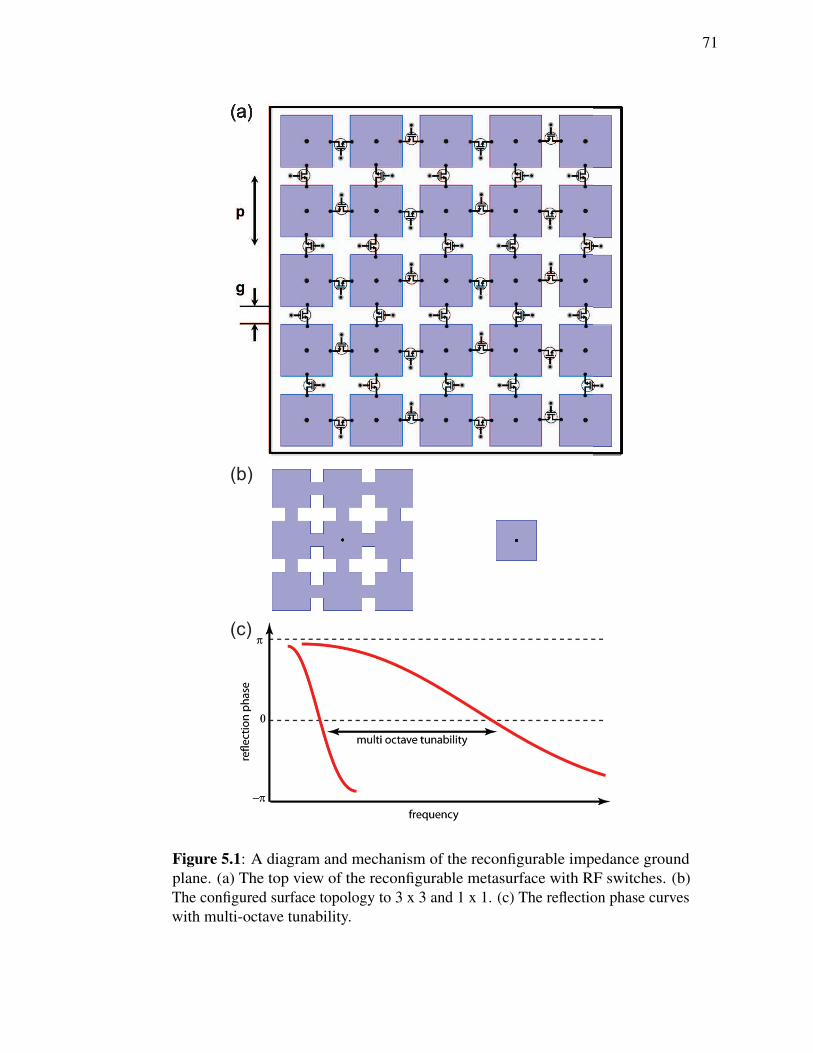
71
(a)
(b)
(c)
Figure 5.1: A diagram and mechanism of the reconfigurable impedance groundplane. (a) The top view of the reconfigurable metasurface with RF switches. (b)The configured surface topology to 3 x 3 and 1 x 1. (c) The reflection phase curveswith multi-octave tunability.

72
(b)(a)
Figure 5.2: A scheme of the reconfigurable surface topology. (a) An example of 2x 2 surface topology. (b) A brief circuit scheme on the metasurface to control theRF MOSEFET switch.
wideband tunable surface, as shown in Fig. 5.1 (a). The reconfigurable structure consists of
two-dimensional metallic patches connected by RF MOSFETs. The patch has p = 3.2mm
as a period and g = 0.81mm as a gap distance. By applying transistors to the impedance
surface rather than varactors, they exhibit high linearity due to their discrete on/off states
and their extreme wideband tuning performance by manipulating the surface topology as
shown in Fig. 5.1 (b). For instance, manipulated reconfigured schemes of 3 x 3 and 1 x 1 are
shown for low and high resonance frequencies, where the reflection phase crosses through
zero, respectively. This is also the frequency where antennas located near the surface will
operate efficiently. The reflection phase curves for two different high impedance surfaces
with the different resonance frequencies are shown in Fig. 5.1 (c). By reconfiguring the
surface between these two states, or any state in between, we can tune the antenna response
over a wide range of frequencies. In other words, the MOSFETs based reconfigurable
plane can form N x N configurations by shorting adjacent patches, and thus, it is tuned in a
digital manner to show multi-octave tunability from a single patch to the larger patches. For
example, the manipulation of the 2 x 2 configuration has been done to turn on/off the RF
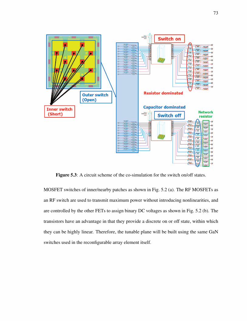
73
Figure 5.3: A circuit scheme of the co-simulation for the switch on/off states.
MOSFET switches of inner/nearby patches as shown in Fig. 5.2 (a). The RF MOSFETs as
an RF switch are used to transmit maximum power without introducing nonlinearities, and
are controlled by the other FETs to assign binary DC voltages as shown in Fig. 5.2 (b). The
transistors have an advantage in that they provide a discrete on or off state, within which
they can be highly linear. Therefore, the tunable plane will be built using the same GaN
switches used in the reconfigurable array element itself.
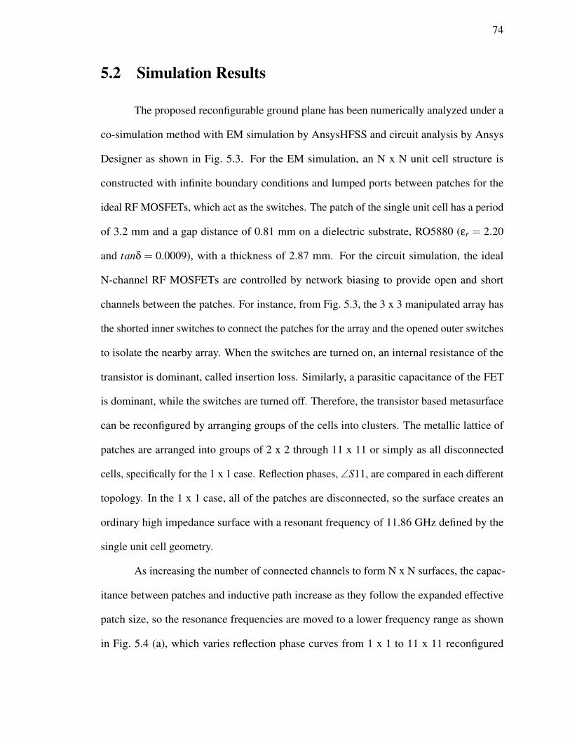
74
5.2 Simulation Results
The proposed reconfigurable ground plane has been numerically analyzed under a
co-simulation method with EM simulation by AnsysHFSS and circuit analysis by Ansys
Designer as shown in Fig. 5.3. For the EM simulation, an N x N unit cell structure is
constructed with infinite boundary conditions and lumped ports between patches for the
ideal RF MOSFETs, which act as the switches. The patch of the single unit cell has a period
of 3.2 mm and a gap distance of 0.81 mm on a dielectric substrate, RO5880 (εr = 2.20
and tanδ = 0.0009), with a thickness of 2.87 mm. For the circuit simulation, the ideal
N-channel RF MOSFETs are controlled by network biasing to provide open and short
channels between the patches. For instance, from Fig. 5.3, the 3 x 3 manipulated array has
the shorted inner switches to connect the patches for the array and the opened outer switches
to isolate the nearby array. When the switches are turned on, an internal resistance of the
transistor is dominant, called insertion loss. Similarly, a parasitic capacitance of the FET
is dominant, while the switches are turned off. Therefore, the transistor based metasurface
can be reconfigured by arranging groups of the cells into clusters. The metallic lattice of
patches are arranged into groups of 2 x 2 through 11 x 11 or simply as all disconnected
cells, specifically for the 1 x 1 case. Reflection phases, ∠S11, are compared in each different
topology. In the 1 x 1 case, all of the patches are disconnected, so the surface creates an
ordinary high impedance surface with a resonant frequency of 11.86 GHz defined by the
single unit cell geometry.
As increasing the number of connected channels to form N x N surfaces, the capac-
itance between patches and inductive path increase as they follow the expanded effective
patch size, so the resonance frequencies are moved to a lower frequency range as shown
in Fig. 5.4 (a), which varies reflection phase curves from 1 x 1 to 11 x 11 reconfigured

75
0 2 4 6 8 10 12 14 16 18−π
−π/2
0
π/2
π
Frequency [GHz]
Re
!e
ctio
n P
ha
se
1Χ1
2Χ2
3Χ3
4Χ4
5Χ5
6Χ6
7Χ7
8Χ8
9Χ9
10Χ10
11Χ11
0 2 4 6 8 10 12 14 16 18−π
−π/2
0
π/2
π
Frequency [GHz]
Re
!e
ctio
n P
ha
se
(a)
(b) (c)
Figure 5.4: Simulation results of the reconfigurable ground plane with the idealRF switches. (a) Reflection phase of N x N surface topology. E-field profiles of (b)3 x 3 and (c) 1 x 1 configurations.
impedance ground plane. The reflection phase bandwidth determined from −π/2 to π/2 in
each configured surface is slightly overlapped by neighboring bandwidth. For example, the
tuned surfaces of 1 x 1 and 2 x 2 patterns have the bandwidth of 8.75 - 17.4 GHz and 5.85 -
8.8 GHz, respectively, so the bandwidth of the lower edge of 1 x 1 and the upper edge of 2 x
2 is superposed at 0.05 GHz. Therefore, the reconfigurable plane can operate as an artificial
magnetic conductor across the tunable frequency range from 2 to 17 GHz within the shaded
region as shown in Fig. 5.4 (a). E-field profiles on the surface for different arrangements of
the unit cells are plotted under the same scale as shown in Fig. 5.4 (b) and (c). Fig. 5.4 (b)
76
shows the E-field magnitude of the 3 x 3 topology at the resonance frequency 5.19 GHz,
while Fig. 5.4 (c) represents the 1 x 1 pattern at 11.85 GHz. The surface field profiles verify
that the surfaces configured by applying the network bias have tunable reflection phase
states.
5.3 Prototype Reconfigurable Surface
The proposed reconfigurable metasurface with the ideal RF MOSFETs enables
covering the extreme frequency band from 2 to 17 GHz. The parasitic values such as an
internal resistance, capacitance, and inductance, however, can affect the desired performance.
Therefore, a prototype board was built to verify the operation of the impedance manipulation
by changing the configuration of the network RF transistors. The fabricated board consists
of 6 x 6 array and the geometry of the unit cell patch of the sample is 18 mm of the period
and 2.5 mm of the gap distance on the RO5880 material with 3.175 mm thickness. The
operation frequency in maintaining the artificial magnetic conductor is from 1.5 to 5 GHz.
5.3.1 Simulation Data of Prototype Sample
The co-simulation data of the fabricated prototype metasurface is shown in Fig. 5.5.
The reflection phase of the prototype structure has three different states of 1 x 1 to 3 x 3
configurations which were designed to operate over several waveguide bands, WR650 (1.15
- 1.72 GHz), WR430 (1.72 - 2.60 GHz), and WR284 (2.60 - 3.95 GHz), for measurement.
Fig. 5.5 (a) represents the reflection phases with the ideal switches, while Fig. 5.5 (b) shows
the simulation data with parasitic values of the RF switch, Skyworks SKY13347-360LF.
The values of the parasitic are Ron = 3ω and C = 0.1pF , respectively. The reflection phases

77
0 1 2 3 4 5 6−π
−π/2
0
π/2
π
Frequency [GHz]
Re
!e
ctio
n P
ha
se
1 1
2 2
3Χ3
0 1 2 3 4 5 6−π
−π/2
0
π/2
π
Frequency [GHz]
Re
!e
ctio
n P
ha
se
0 1 2 3 4 5 6−π
−π/2
0
π/2
π
Frequency [GHz]
Re
!e
ctio
n P
ha
se
1 1
2 2
3 3
0 1 2 3 4 5 6−π
−π/2
0
π/2
π
Frequency [GHz]
Re
!e
ctio
n P
ha
se
(b)
(a)
Χ
Χ
Χ
Χ
Χ
Figure 5.5: Simulation results of the prototype structure. Reflection phase with (a)the ideal RF switches and (b) the actual RF MOSFET including parasitic values.
with the actual SPICE model of the RF switch are shown of the shift to the lower frequency
due to the parasitic effects.
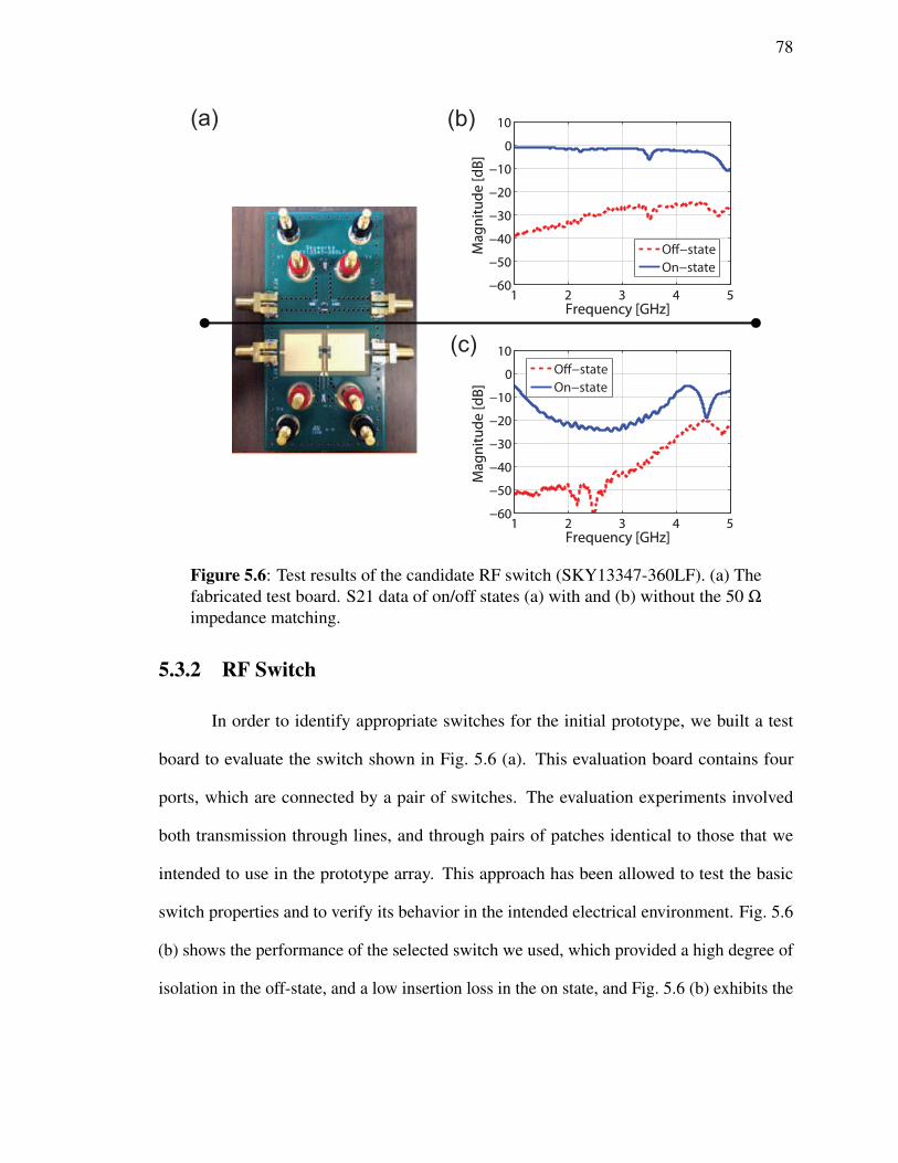
78
1 2 3 4 5−60
−50
−40
−30
−20
−10
0
10
Frequency [GHz]
Ma
gn
itu
de
[d
B]
O!−state
On−state
1 2 3 4 5−60
−50
−40
−30
−20
−10
0
10
Frequency [GHz]
Ma
gn
itu
de
[d
B]
1 2 3 4 5−60
−50
−40
−30
−20
−10
0
10
Frequency [GHz]
Ma
gn
itu
de
[d
B]
O!−state
On−state
1 2 3 4 5−60
−50
−40
−30
−20
−10
0
10
Frequency [GHz]
Ma
gn
itu
de
[d
B]
(a) (b)
(c)
Figure 5.6: Test results of the candidate RF switch (SKY13347-360LF). (a) Thefabricated test board. S21 data of on/off states (a) with and (b) without the 50 Ω
impedance matching.
5.3.2 RF Switch
In order to identify appropriate switches for the initial prototype, we built a test
board to evaluate the switch shown in Fig. 5.6 (a). This evaluation board contains four
ports, which are connected by a pair of switches. The evaluation experiments involved
both transmission through lines, and through pairs of patches identical to those that we
intended to use in the prototype array. This approach has been allowed to test the basic
switch properties and to verify its behavior in the intended electrical environment. Fig. 5.6
(b) shows the performance of the selected switch we used, which provided a high degree of
isolation in the off-state, and a low insertion loss in the on state, and Fig. 5.6 (b) exhibits the

79
DC bias port in column
DC
bia
s p
ort
in
ro
w
DC bias port for
supply voltage
GND port
VNA
DC source
WG
S11
Metasurface
(a) (b)
Figure 5.7: Measurement setup of the prototype reconfigurable impedance plane.(a) A photo of the prototype sample. (b) A brief scheme of the measurementsystem.
1x1 2x2 3x3
(a) (b) (c)
Figure 5.8: Photos of the reconfigured surface topology by assigning DC bias to(a) 1 x 1, (b) 2 x 2, and (c) 3 x 3.
S21 of on-off states while connecting to the actual patches. Thus, this switch was eventually
selected for the initial prototype tunable ground plane after verifying the performance of the
switch compared with the specifications described by the manufacturer.
5.3.3 Measurement
After selecting the transistor that provided the best performance, the test board which
consisted of a 6 x 6 array of patches, has been fabricated, and each patch is connected to
its neighbors by transistors with control lines arranged around the outside edge as shown
in Fig. 5.7 (a). The measurement setup for the prototype sample is shown in Fig. 5.7
(b) including VNA to measure reflection phase, ∠S11, and DC source to control the RF

80
3.95 4.5 5 5.5 5.85−π
−π/2
0
π/2
π
Frequency [GHz]
Ph
ase
[D
eg
.]
1Χ1
All Shorted
3.95 4.5 5 5.5 5.85−π
−π/2
0
π/2
π
Frequency [GHz]
Ph
ase
[D
eg
.]
(a)
(b)
Figure 5.9: Measurement data of the prototype reconfigurable impedance groundplane. (a) The area of the switchable ground plane compared to various waveguidesizes that are indicated by red, blue, and yellow colored rectangles. (b) The blueand red lines represent the reflection phase of the 1 x 1 configuration and all shortedlarge patch such as a PEC.

81
MOSFETs. The board contained the dielectric substrate for the patches, as well as several
other layers for the control lines, which were fed through the ground plane using vertical
vias. The vias provide the gate contacts for the transistors.
By assigning DC voltages to the control lines in a row and column format, the
tunable ground plane is capable of connecting or disconnecting various groups of patches
by turning on or off the appropriate transistors. Fig. 5.8 shows the board tuned to the
simple (a) 1 x 1 configuration, in which all transistors are off, and the (b) 2 x 2 and (c) 3
x 3 configurations, in which the transistors are turned off in every alternate row and every
alternate column. Because of the control scheme we developed, only 2N control lines are
required to address an N x N array of cells. The surface was initially tested to determine if
the transistors were properly adjusting the conductivity between the plates. It was easily
verified that the plates could be connected or disconnected row by column as intended. By
connecting the appropriate bias lines, the plates could be arranged in 1 x 1, 2 x 2, or 3 x 3
clusters.
From the measurement, the ordinary open-ended waveguides have been used to
measure the reflection phase. First, the waveguide against a flat metal surface is placed for
calibration, and then the open ports were placed above the tunable metasurface to measure
the switching between various states. Note in Fig. 5.9 (a) that each waveguide cross-section,
indicated by various colored rectangles, covers only a small number of unit cells. In the
highest band, the waveguide only covers eight cells in the 1 x 1 configuration, whereas in
the lowest band, the waveguide is only partially filled by the tunable surface. Only in the
mid-band, the waveguide can completely cover the tunable surface, but even in that instance
it only covers 24 cells in the 1 x 1 case, and only six cells in the 2 x 2 case. With such
a small prototype sample, the area is hardly enough to obtain a good measurement of the
82
reflection phase. Nonetheless, the measurement enables to successful detection of the phase
differences between various states. Fig. 5.9 (b) shows the comparison of two cases, in which
none of the switches are closed, corresponding to the 1 x 1 case, and in which all of the
switches are closed, corresponding to a fully conducting surface. A resonance is seen at
around 4 GHz, which can be switched on and off electronically by changing the switch
states. Unfortunately, for larger cell cluster the resonance frequencies are even lower, and
we are not able to obtain reliable measurements below this frequency band due to the size of
the surface.
5.4 Conclusion
In this paper, we demonstrate a novel transistor based metasurface for the reconfig-
urable impedance ground plane. By connecting the multiple metallic patches together, the
surface can be tuned to cover a wide range of the different resonance frequencies. The tuning
range of the surface is from 2 to 17 GHz. From the prototype sample of the reconfigurable
ground plane, the configuration enables the tunable impedance topology by manipulating
the RF switches. Thus, the reconfigurable surface will provide advantages to broadband
tunable antenna systems by tuning the ground plane itself.
Chapter 5 is based on and is mostly a reprint of the following paper: S. Kim, A. Li, D.
Sievenpiper, ”Reconfigurable Impedance Ground Plane for Broadband Antenna Systems”,
2017 IEEE Antennas and Propagation Symposium, San Diego, CA, July 9, 2017. The
dissertation author was the primary author of the work in this chapter, and the co-authors
have approved the use of the material for this dissertation.

Chapter 6
Omni-Directional Metamaterial Surface
In previous chapters, the proposed metamaterial surfaces had a specific direction
preference, such as the switchable absorbing metasurface responding to an incident wave in
a parallel direction. Similarly, the self-tuning metasurface and reconfigurable ground plane
can react to an incoming wave in a normal direction. In practical applications, the direction
of incoming waves does not specify the ideal cases, in both normal and parallel directions.
Therefore, there is the demand to consider a new type of metasurface to absorb illuminated
microwaves, which are incoming toward the metasurface in arbitrary angles. Therefore, the
new metasurface is applicable in all directions, including for the azimuthal (ϕ : 0−2π) and
elevation (θ : 0− π
2 ) angles as shown in Fig. 6.1.
6.1 Background and Motivation
The metasurfaces used in this thesis are based on the high impedance surface, and
the reflection phase shifted to a lower frequency as a result of increases in the incident
angles from 0 (normal) to 2π (parallel) [50, 57, 58]. In practical use of the metasurface,
83
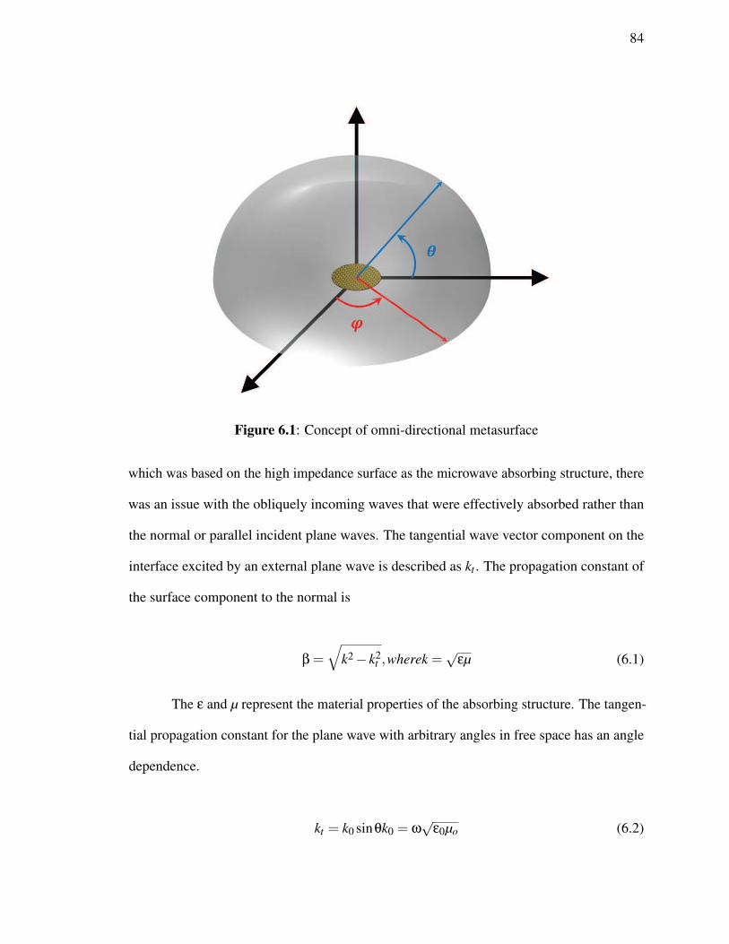
84
Figure 6.1: Concept of omni-directional metasurface
which was based on the high impedance surface as the microwave absorbing structure, there
was an issue with the obliquely incoming waves that were effectively absorbed rather than
the normal or parallel incident plane waves. The tangential wave vector component on the
interface excited by an external plane wave is described as kt . The propagation constant of
the surface component to the normal is
β =
√k2− k2
t ,wherek =√
εµ (6.1)
The ε and µ represent the material properties of the absorbing structure. The tangen-
tial propagation constant for the plane wave with arbitrary angles in free space has an angle
dependence.
kt = k0 sinθk0 = ω√
ε0µo (6.2)

85
Figure 6.2: TE and TM polarization plane waves to high impedance surface
Therefore, if the incident angle of the plane wave is increased, the β is decreased.
In other words, the electrical thickness of the absorbing surface is also decreased, so the
resonance absorber like the Salisbury screen with the quarter wavelength distance from the
grounded planes exhibits different resonance frequencies depending on the different incident
angles.
With the conventional high impedance surface, the unit cell is consisted of a periodic
metallic patch and conducting via shorted to the grounded plane. With the incident plane
waves with oblique angles to the surface, we have to distinguish between the two different
polarizations, the transverse electric (TE) and transverse magnetic (TM) polarized waves
as shown in Fig. 6.2. The electric field of the TE polarized plane wave to the surface is
orthogonal to the conducting via of the high impedance surface. When the TE waves are
incident in the normal direction of the surface, the result is a no-current flow. In other words,
the characteristics of the high impedance surface are same, even on a structure without vias.
In Fig. 6.2, the surface impedance of the TE and TM polarized waves with the oblique
angles are derived below.
ZT Es =
η0
jα(εr +1)cos2 θ(6.3)
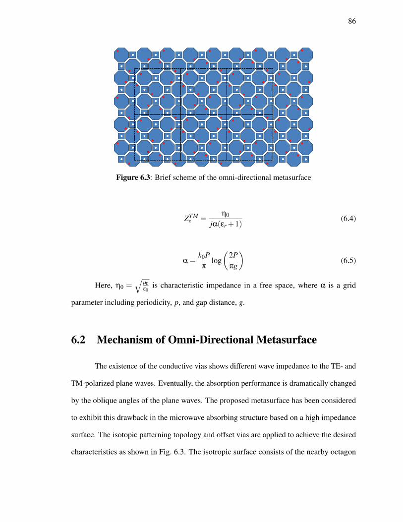
86
Figure 6.3: Brief scheme of the omni-directional metasurface
ZT Ms =
η0
jα(εr +1)(6.4)
α =k0Pπ
log(
2Pπg
)(6.5)
Here, η0 =√
µ0ε0
is characteristic impedance in a free space, where α is a grid
parameter including periodicity, p, and gap distance, g.
6.2 Mechanism of Omni-Directional Metasurface
The existence of the conductive vias shows different wave impedance to the TE- and
TM-polarized plane waves. Eventually, the absorption performance is dramatically changed
by the oblique angles of the plane waves. The proposed metasurface has been considered
to exhibit this drawback in the microwave absorbing structure based on a high impedance
surface. The isotopic patterning topology and offset vias are applied to achieve the desired
characteristics as shown in Fig. 6.3. The isotropic surface consists of the nearby octagon
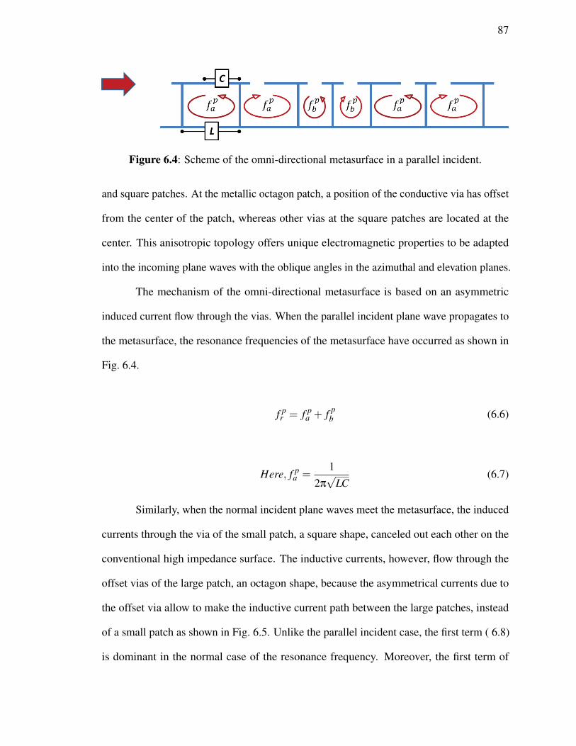
87
Figure 6.4: Scheme of the omni-directional metasurface in a parallel incident.
and square patches. At the metallic octagon patch, a position of the conductive via has offset
from the center of the patch, whereas other vias at the square patches are located at the
center. This anisotropic topology offers unique electromagnetic properties to be adapted
into the incoming plane waves with the oblique angles in the azimuthal and elevation planes.
The mechanism of the omni-directional metasurface is based on an asymmetric
induced current flow through the vias. When the parallel incident plane wave propagates to
the metasurface, the resonance frequencies of the metasurface have occurred as shown in
Fig. 6.4.
f pr = f p
a + f pb (6.6)
Here, f pa =
12π√
LC(6.7)
Similarly, when the normal incident plane waves meet the metasurface, the induced
currents through the via of the small patch, a square shape, canceled out each other on the
conventional high impedance surface. The inductive currents, however, flow through the
offset vias of the large patch, an octagon shape, because the asymmetrical currents due to
the offset via allow to make the inductive current path between the large patches, instead
of a small patch as shown in Fig. 6.5. Unlike the parallel incident case, the first term ( 6.8)
is dominant in the normal case of the resonance frequency. Moreover, the first term of

88
Figure 6.5: Scheme of the omni-directional metasurface in a normal incident.
the normal resonance frequency coincides as the the first them of the parallel resonance
frequencies of ( 6.9) , ( 6.10), and ( 6.11)
f nr = f n
c + f nd (6.8)
Here, f nc =
12π√
2L(C/2)=
12π√
LC(6.9)
f nc = f p
b (6.10)
f nr = f n
c + f nd∼= f p
b (6.11)
Therefore, the overall resonance frequencies in the extreme cases, both parallel and
normal incidents, have coincidences, that can be applicable to the adaptive oblique incident
angle cases.
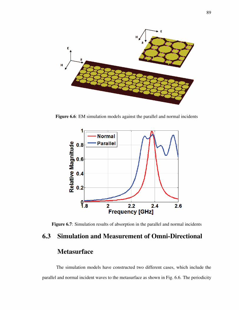
89
Figure 6.6: EM simulation models against the parallel and normal incidents
Figure 6.7: Simulation results of absorption in the parallel and normal incidents
6.3 Simulation and Measurement of Omni-Directional
Metasurface
The simulation models have constructed two different cases, which include the
parallel and normal incident waves to the metasurface as shown in Fig. 6.6. The periodicity
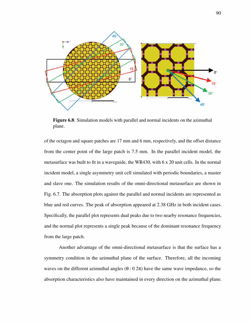
90
Figure 6.8: Simulation models with parallel and normal incidents on the azimuthalplane.
of the octagon and square patches are 17 mm and 6 mm, respectively, and the offset distance
from the center point of the large patch is 7.5 mm. In the parallel incident model, the
metasurface was built to fit in a waveguide, the WR430, with 6 x 20 unit cells. In the normal
incident model, a single asymmetry unit cell simulated with periodic boundaries, a master
and slave one. The simulation results of the omni-directional metasurface are shown in
Fig. 6.7. The absorption plots against the parallel and normal incidents are represented as
blue and red curves. The peak of absorption appeared at 2.38 GHz in both incident cases.
Specifically, the parallel plot represents dual peaks due to two nearby resonance frequencies,
and the normal plot represents a single peak because of the dominant resonance frequency
from the large patch.
Another advantage of the omni-directional metasurface is that the surface has a
symmetry condition in the azimuthal plane of the surface. Therefore, all the incoming
waves on the different azimuthal angles (θ : 0 2π) have the same wave impedance, so the
absorption characteristics also have maintained in every direction on the azimuthal plane.

91
Figure 6.9: Simulation data with different azimuthal angles in parallel and normalincoming waves.
The simulation models have been constructed to adapt the parallel and normal incident
waves with different azimuthal angles as shown in Fig. 6.8. For the parallel incident, a large
circular surface was built symmetrically periodic impedance on the plane. The large circular
panel was cut to four different sections with 0, 15, 30, and 45 to cover all the possible
directions in the azimuthal plane. For the normal incident, input waves in the simulation
setup have assigned with the azimuthal angles the same values as the parallel case. The
simulation data of the absorption peak under different azimuthal directions are shown in
Fig. 6.9. From the simulation results, either parallel or normal incoming plane waves are
highly absorbed around 2.38 GHz by the omni-directional metasurface.
Based on the numerical approach, the prototype omni-directional metasurfaces were
built for absorption measurement as shown in Fig. 6.10. The two prototype samples were
fabricated to fit into the waveguide, WR430. The large and small samples in Fig. 6.10
represent the incoming waves in the parallel and the normal directions, respectively. Re-
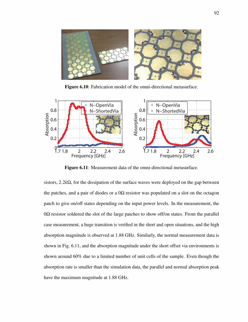
92
Figure 6.10: Fabrication model of the omni-directional metasurface.
1.7 1.8 2 2.2 2.4 2.60
0.2
0.4
0.6
0.8
1
Frequency [GHz]
Ab
sorp
tio
n
N−OpenVia
N−ShortedVia
1.7 1.8 2 2.2 2.4 2.60
0.2
0.4
0.6
0.8
1
Frequency [GHz]
Ab
sorp
tio
n
1.7 1.8 2 2.2 2.4 2.60
0.2
0.4
0.6
0.8
1
Frequency [GHz]
Ab
sorp
tio
n
N−OpenVia
N−ShortedVia
1.7 1.8 2 2.2 2.4 2.60
0.2
0.4
0.6
0.8
1
Frequency [GHz]
Ab
sorp
tio
n
Figure 6.11: Measurement data of the omni-directional metasurface.
sistors, 2.2kΩ, for the dissipation of the surface waves were deployed on the gap between
the patches, and a pair of diodes or a 0Ω resistor was populated on a slot on the octagon
patch to give on/off states depending on the input power levels. In the measurement, the
0Ω resistor soldered the slot of the large patches to show off/on states. From the parallel
case measurement, a huge transition is verified in the short and open situations, and the high
absorption magnitude is observed at 1.88 GHz. Similarly, the normal measurement data is
shown in Fig. 6.11, and the absorption magnitude under the short offset via environments is
shown around 60% due to a limited number of unit cells of the sample. Even though the
absorption rate is smaller than the simulation data, the parallel and normal absorption peak
have the maximum magnitude at 1.88 GHz.
93
6.4 Conclusion
In this chapter, we demonstrate a novel metasurface for adapting incoming plane
waves in all directions for practical applications. By applying the anisotropic surface
topology and an offset via concept, the metasurface responded to the incident waves with
all oblique angles including the azimuthal and elevation planes. Thus, the proposed omni-
directional metasurface can be applicable to even or curvature surfaces, advanced antenna
systems to minimize the surface currents, and other possible implementations.
Chapter 6 is based on and is mostly a reprint of the following paper: S. Kim, A. Li,
D. Sievenpiper, Omni-directional metamaterial surface, in preparation. The dissertation
author was the primary author of the work in this chapter, and the co-authors have approved
the use of the material for this dissertation.
Chapter 7
Conclusion
7.1 Summary of Work
This thesis presents a comprehensive overview of the advantages and implementa-
tions of the nonlinear active metamaterial surfaces.
Chapter 1 introduced the motivation of the research and the advantages of using a
metamaterial surface for application in microwave absorbing structures.
Chapter 2 addressed the theoretical limitations for the TM surface wave attenuation
while applying an impedance sheet on the grounded dielectric substrate. The analytical
solutions derived were based on Maxwell’s equations. The solutions were verified with by
numerical simulation methods in Ansys HFSS.
Chapter 3 presented a power dependent metamaterial absorber. A pair of series
diodes are embedded on the metasurface, and it played a role in the switch depending
on input power levels. In other words, if the high power inputs were incoming to the
metasurface, the surface is transformed to an absorber. On the other hand, the metallic
structure worked ordinary metal sheet when low powers were illuminated on the surface.
94
95
Chapter 4 examined the theory and concept of the self-tuning metasurface. The novel
metasurface is divided into parts to adapt to incoming frequencies. The sensing circuit part
is a kind of feedback circuit used to generate proper DC bias to control the varactor diodes
for tuning. Therefore, the self-tuning metasurface can be achievable for the broadband
absorbing application.
Chapter 5 studied a transistor based ground plane. The reconfigurable surface
can be manipulated by RF MOSFET switches between the patches. After modifying the
impedance topology of the surface, the reconfigurable plane had an octave tunability to cover
an extreme broadband frequency range. The metasurface can be applicable to broadband
antenna systems and multi-antennas sharing the same ground plane.
Chapter 6 presented an omni-directional metasurface to respond to all incoming
waves with oblique angles. To achieve that goal, anisotropic topology and offset vis concepts
were applied to the metasurface.
7.2 Future Work
Adapting nonlinear circuit components to metamaterial surfaces can make unique
electromagnetic performances possible such as the power dependent absorber, self-tunability,
and all directional responses. However, most of the circuit components have internal parasitic
parameters, and the parasitic values cause unexpected drawbacks, higher harmonics, and
internal losses. Therefore, minimizing or canceling the parasitic circuit like a non-Foster
circuit will expand the implementations into various fields.

Bibliography
[1] Scientific American: Supplement. Munn and Company, 1917, no. v. 84.
[2] D. F. Sievenpiper, “Nonlinear grounded metasurfaces for suppression of high-powerpulsed rf currents,” IEEE Antennas and Wireless Propagation Letters, vol. 10, pp.1516–1519, 2011.
[3] S. W, “Absorbent body for electromagnetic waves,” Jun. 10 1952, uS Patent 2,599,944.[Online]. Available: https://www.google.com/patents/US2599944
[4] R. L. Fante and M. T. McCormack, “Reflection properties of the salisbury screen,”IEEE Transactions on Antennas and Propagation, vol. 36, no. 10, pp. 1443–1454, Oct1988.
[5] R. Gilbert, “Thin, broadband salisbury screen absorber,” Mar. 25 2003, uS Patent6,538,596. [Online]. Available: https://www.google.com/patents/US6538596
[6] D. Sievenpiper, L. Zhang, R. F. J. Broas, N. G. Alexopolous, and E. Yablonovitch,“High-impedance electromagnetic surfaces with a forbidden frequency band,” IEEETransactions on Microwave Theory and Techniques, vol. 47, no. 11, pp. 2059–2074,Nov 1999.
[7] F. Costa, A. Monorchio, and G. Manara, “Analysis and design of ultra thin electro-magnetic absorbers comprising resistively loaded high impedance surfaces,” IEEETransactions on Antennas and Propagation, vol. 58, no. 5, pp. 1551–1558, May 2010.
[8] N. I. Landy, S. Sajuyigbe, J. J. Mock, D. R. Smith, and W. J. Padilla, “Perfect metama-terial absorber,” Phys. Rev. Lett., vol. 100, p. 207402, May 2008.
[9] V. G. Veselago, “The electrodynamics of substances with simultaneously negativevalues e and u,” Sov. Phys. Uspekhi, vol. 10, no. 4, p. 509, 1968.
[10] R. A. Shelby, D. R. Smith, and S. Schultz, “Experimental verification of a negativeindex of refraction,” Science, vol. 292, no. 5514, pp. 77–79, 2001.
[11] D. Schurig, J. Mock, B. Justice, S. Cummer, J. Pendry, A. Starr, and D. Smith,“Metamaterial electromagnetic cloak at microwave frequencies,” Science, vol. 314, no.5801, pp. 977–980, 11 2006.
96
97
[12] M. C. K. Wiltshire, J. B. Pendry, I. R. Young, D. J. Larkman, D. J. Gilderdale, and J. V.Hajnal, “Microstructured magnetic materials for rf flux guides in magnetic resonanceimaging,” Science, vol. 291, no. 5505, pp. 849–851, 2001.
[13] D. R. Smith, W. J. Padilla, D. C. Vier, S. C. Nemat-Nasser, and S. Schultz, “Compositemedium with simultaneously negative permeability and permittivity,” Phys. Rev. Lett.,vol. 84, pp. 4184–4187, May 2000.
[14] M. Gokkavas, K. Guven, I. Bulu, K. Aydin, R. S. Penciu, M. Kafesaki, C. M. Soukoulis,and E. Ozbay, “Experimental demonstration of a left-handed metamaterial operating at100 GHz,” Phys. Rev. B, vol. 73, p. 193103, May 2006.
[15] T. J. Yen, W. J. Padilla, N. Fang, D. C. Vier, D. R. Smith, J. B. Pendry, D. N. Basov,and X. Zhang, “Terahertz magnetic response from artificial materials,” Science, vol.303, no. 5663, pp. 1494–1496, 2004.
[16] S. Zhang, W. Fan, N. C. Panoiu, K. J. Malloy, R. M. Osgood, and S. R. J. Brueck,“Experimental demonstration of near-infrared negative-index metamaterials,” Phys.Rev. Lett., vol. 95, p. 137404, Sep 2005.
[17] G. Dolling, M. Wegener, C. M. Soukoulis, and S. Linden, “Negative-index metamate-rial at 780 nm wavelength,” Opt. Lett., vol. 32, no. 1, pp. 53–55, Jan 2007.
[18] V. M. Shalaev, W. Cai, U. K. Chettiar, H.-K. Yuan, A. K. Sarychev, V. P. Drachev, andA. V. Kildishev, “Negative index of refraction in optical metamaterials,” Opt. Lett.,vol. 30, no. 24, pp. 3356–3358, Dec 2005.
[19] J. B. Pendry, “Negative refraction makes a perfect lens,” Phys. Rev. Lett., vol. 85, pp.3966–3969, Oct 2000.
[20] Y. S. K. Nikolay I. Zheludev, “From metamaterials to metadevices,” Nature Materials,vol. 11, pp. 917–924, October 2012.
[21] A. V. Kildishev, A. Boltasseva, and V. M. Shalaev, “Planar photonics with metasurfaces,”Science, vol. 339, no. 6125, 2013.
[22] N. Yu, P. Genevet, M. A. Kats, F. Aieta, J.-P. Tetienne, F. Capasso, and Z. Gaburro,“Light propagation with phase discontinuities: Generalized laws of reflection andrefraction,” Science, vol. 334, no. 6054, pp. 333–337, 2011.
[23] P. Genevet, N. Yu, F. Aieta, J. Lin, M. A. Kats, R. Blanchard, M. O. Scully, Z. Gaburro,and F. Capasso, “Ultra-thin plasmonic optical vortex plate based on phase discontinu-ities,” Applied Physics Letters, vol. 100, no. 1, p. 013101, 2012.
[24] E. H. Khoo, E. P. Li, and K. B. Crozier, “Plasmonic wave plate based on subwavelengthnanoslits,” Opt. Lett., vol. 36, no. 13, pp. 2498–2500, Jul 2011.

98
[25] Y. Zhao and A. Alu, “Manipulating light polarization with ultrathin plasmonic meta-surfaces,” Phys. Rev. B, vol. 84, p. 205428, Nov 2011.
[26] Y. Liu and X. Zhang, “Metasurfaces for manipulating surface plasmons,” AppliedPhysics Letters, vol. 103, no. 14, p. 141101, 2013.
[27] S. B. Glybovski, S. A. Tretyakov, P. A. Belov, Y. S. Kivshar, and C. R. Simovski,“Metasurfaces: From microwaves to visible,” Physics Reports, vol. 634, pp. 1 – 72,2016, metasurfaces: From microwaves to visible.
[28] C. Balanis, “Advanced enginerring electromechanics,” 1989.
[29] G. Goubau, “Surface waves and their application to transmission lines,” Journal ofApplied Physics, vol. 21, no. 11, pp. 1119–1128, 1950.
[30] C. A. Balanis, Antenna theory: analysis and design. John Wiley & Sons, 2016.
[31] A. Vallecchi, J. R. D. Luis, F. Capolino, and F. D. Flaviis, “Low profile fully planarfolded dipole antenna on a high impedance surface,” IEEE Transactions on Antennasand Propagation, vol. 60, no. 1, pp. 51–62, Jan 2012.
[32] S. S. Attwood, “Surfacewave propagation over a coated plane conductor,” Journal ofApplied Physics, vol. 22, no. 4, pp. 504–509, 1951.
[33] K. N. Rozanov, “Ultimate thickness to bandwidth ratio of radar absorbers,” IEEETransactions on Antennas and Propagation, vol. 48, no. 8, pp. 1230–1234, Aug 2000.
[34] B. A. Munk, Frequency selective surfaces. John Wiley & Sons, 2005.
[35] C. L. Holloway, D. C. Love, E. F. Kuester, J. A. Gordon, and D. A. Hill, “Use of gener-alized sheet transition conditions to model guided waves on metasurfaces/metafilms,”IEEE Transactions on Antennas and Propagation, vol. 60, no. 11, pp. 5173–5186, Nov2012.
[36] R. E. Collin, Foundations for microwave engineering. John Wiley & Sons, 2007.
[37] G. Goussetis, J. L. Gomez-Tornero, A. P. Feresidis, and N. K. Uzunoglu, “Artifi-cial impedance surfaces for reduced dispersion in antenna feeding systems,” IEEETransactions on Antennas and Propagation, vol. 58, no. 11, pp. 3629–3636, Nov 2010.
[38] W. B. Weir, “Automatic measurement of complex dielectric constant and permeabilityat microwave frequencies,” Proceedings of the IEEE, vol. 62, no. 1, pp. 33–36, Jan1974.
[39] G. T. Ruck, D. E. Barrick, W. D. Stuart, and C. K. Krichbaum, Radar cross sectionhandbook. Plenum press New York, 1970, vol. 1.
[40] E. F. Knott, Radar cross section measurements. Springer Science & Business Media,2012.

99
[41] and others, “Absorbent body for electromagnetic waves,” Jun. 10 1952, uS Patent2,599,944.
[42] B. A. Munk, “Frequency selective surfaces theory and design. john wiley&sons,” 2000.
[43] H. Tao, N. I. Landy, C. M. Bingham, X. Zhang, R. D. Averitt, and W. J. Padilla, “Ametamaterial absorber for the terahertz regime: Design, fabrication and characteriza-tion,” Optics express, vol. 16, no. 10, pp. 7181–7188, 2008.
[44] H. Li, L. H. Yuan, B. Zhou, X. P. Shen, Q. Cheng, and T. J. Cui, “Ultrathin multibandgigahertz metamaterial absorbers,” Journal of Applied Physics, vol. 110, no. 1, p.014909, 2011.
[45] F. Ding, Y. Cui, X. Ge, Y. Jin, and S. He, “Ultra-broadband microwave metamaterialabsorber,” Applied physics letters, vol. 100, no. 10, p. 103506, 2012.
[46] S. Kim and D. F. Sievenpiper, “Theoretical limitations for tm surface wave attenua-tion by lossy coatings on conducting surfaces,” IEEE Transactions on Antennas andPropagation, vol. 62, no. 1, pp. 475–480, 2014.
[47] H. Wakatsuchi, S. Kim, J. J. Rushton, and D. F. Sievenpiper, “Circuit-based nonlinearmetasurface absorbers for high power surface currents,” Applied Physics Letters, vol.102, no. 21, p. 214103, 2013.
[48] ——, “Waveform-dependent absorbing metasurfaces,” Physical review letters, vol.111, no. 24, p. 245501, 2013.
[49] Z. Luo, X. Chen, J. Long, R. Quarfoth, and D. Sievenpiper, “Nonlinear power-dependent impedance surface,” IEEE Transactions on Antennas and Propagation,vol. 63, no. 4, pp. 1736–1745, 2015.
[50] D. F. Sievenpiper, J. H. Schaffner, H. J. Song, R. Y. Loo, and G. Tangonan, “Two-dimensional beam steering using an electrically tunable impedance surface,” IEEETransactions on Antennas and Propagation, vol. 51, no. 10, pp. 2713–2722, Oct 2003.
[51] I. Gil, J. Garcia-Garcia, J. Bonache, F. Martin, M. Sorolla, and R. Marques, “Varactor-loaded split ring resonators for tunable notch filters at microwave frequencies,” Elec-tronics Letters, vol. 40, no. 21, pp. 1347–1348, Oct 2004.
[52] O. Reynet and O. Acher, “Voltage controlled metamaterial,” Applied Physics Letters,vol. 84, no. 7, pp. 1198–1200, 2004.
[53] T. Hand and S. Cummer, “Characterization of tunable metamaterial elements usingmems switches,” IEEE Antennas and Wireless Propagation Letters, vol. 6, pp. 401–404,2007.
100
[54] A. R. Katko, J. P. Barrett, and S. A. Cummer, “Time-varying transistor-based meta-material for tunability, mixing, and efficient phase conjugation,” Journal of AppliedPhysics, vol. 115, no. 14, p. 144501, 2014.
[55] F.-R. Yang, K.-P. Ma, Y. Qian, and T. Itoh, “A uniplanar compact photonic-bandgap(uc-pbg) structure and its applications for microwave circuits,” 1999.
[56] G. Goussetis, A. P. Feresidis, and J. C. Vardaxoglou, “Tailoring the amc and ebgcharacteristics of periodic metallic arrays printed on grounded dielectric substrate,”IEEE Transactions on Antennas and Propagation, vol. 54, no. 1, pp. 82–89, Jan 2006.
[57] S. A. Tretyakov and S. I. Maslovski, “Thin absorbing structure for all incidenceangles based on the use of a high-impedance surface,” Microwave and OpticalTechnology Letters, vol. 38, no. 3, pp. 175–178, 2003. [Online]. Available:http://dx.doi.org/10.1002/mop.11006
[58] O. Luukkonen, M. G. Silveirinha, A. B. Yakovlev, C. R. Simovski, I. S. Nefedov,and S. A. Tretyakov, “Effects of spatial dispersion on reflection from mushroom-type artificial impedance surfaces,” IEEE Transactions on Microwave Theory andTechniques, vol. 57, no. 11, pp. 2692–2699, Nov 2009.