Embed Size (px)
Citation preview
NON DESTRUCTIVE SURFACE AND SUB-SURFACE
MATERIAL ANALYSIS USING SCANNING SQUID
MAGNETIC MICROSCOPE
Maria Adamo
DOCTOR OF PHILOSOPHY
AT
UNIVERSITA’ DEGLI STUDI DI NAPOLI
FEDERICO II
ITALY
30TH NOVEMBER 2008

UNIVERSITA’ DEGLI STUDI DI NAPOLI
FEDERICO II
DEPARTMENT OF PHYSICAL SCIENCES
The undersigned hereby certify the acceptance of the thesis
entitled “Non Destructive Surface and Sub-surface Material
Analysis using Scanning SQUID Magnetic Microscope”
by Maria Adamo in partial fulfillment of the requirements for the
degree of Doctor of Philosophy.
Dated: 30th November 2008
PhD Coordinator
Prof. Giancarlo Abbate
Department of Physical Sciences, University of Naples ”Federico II”
PhD Coordinator:
ii

UNIVERSITA’ DEGLI STUDI DI NAPOLI
FEDERICO II
Date: 30th November 2008
Author: Maria Adamo
Title: Non Destructive Surface and Sub-surface Material
Analysis using Scanning SQUID Magnetic
Microscope
Department: Physical Sciences
Degree: Ph.D. Convocation: 19th Dec Year: 2008
The research activity described in this thesis was performed atIstituto di Cibernetica of CNR of Pozzuoli (Napoli), where a semi-commercial Scanning SQUID Microscope prototype has been installed inthe framework of the regional project ”Centro di Competenza Regionaleper la valorizzazione e fruizione dei Beni Culturali e Ambientali” (CRdC-INNOVA).
SupervisorsDr. Ettore Sarnelli and Dr. Roberto CristianoIstituto di Cibernetica of CNR of Pozzuoli, Naples (Italy)
Signature of Author
iii

Who has seen the wind?
Neither I nor you:
But when the leaves hang trembling
The wind is passing thro’.
iv

Table of Contents
Table of Contents v
Abstract vii
Acknowledgements viii
Introduction 1
1 Superconducting Magnetic Sensors 6
1.1 General Aspects . . . . . . . . . . . . . . . . . . . . . . . . . . . 8
1.1.1 Flux quantization . . . . . . . . . . . . . . . . . . . . . . . . . 10
1.1.2 The Josephson junction . . . . . . . . . . . . . . . . . . . . . 11
1.1.3 The Josephson effect . . . . . . . . . . . . . . . . . . . . . . . 13
1.2 Superconducting Quantum Interference Devices (SQUIDs) 18
1.2.1 The dc SQUID . . . . . . . . . . . . . . . . . . . . . . . . . . 19
1.2.2 SQUID readout . . . . . . . . . . . . . . . . . . . . . . . . . . 24
1.2.3 SQUID magnetometers . . . . . . . . . . . . . . . . . . . . . . 26
2 Room-Temperature Scanning SQUID Microscope 32
2.1 Scanning Probe Magnetic Microscopy . . . . . . . . . . . . . 34
2.1.1 Scanning SQUID Microscopy . . . . . . . . . . . . . . . . . . 36
2.1.2 Volumetric energy resolution . . . . . . . . . . . . . . . . . . . 36
2.1.3 Low-Tc and high-Tc SSM . . . . . . . . . . . . . . . . . . . . . 38
2.2 Scanning SQUID Microscope System Design . . . . . . . . . . 41
2.2.1 DC and AC measurements . . . . . . . . . . . . . . . . . . . . 44
2.2.2 Lock-in technique . . . . . . . . . . . . . . . . . . . . . . . . . 47
2.3 Scanning SQUID Microscope Sensor . . . . . . . . . . . . . . . 51
2.3.1 Spatial Resolution and Magnetic Field Sensitivity . . . . . . . 54
v

3 Eddy Current Non Destructive Analysis 59
3.1 Eddy Currents . . . . . . . . . . . . . . . . . . . . . . . . . . . . . 61
3.2 Mathematical Derivation of Eddy Currents . . . . . . . . . 64
3.2.1 Penetration Depth . . . . . . . . . . . . . . . . . . . . . . . . 67
3.2.2 Eddy Current Distribution . . . . . . . . . . . . . . . . . . . . 68
3.3 Eddy Current in Thin Conducting Plates . . . . . . . . . . . 72
3.3.1 Magnetic Field Distribution in a flawed plate . . . . . . . . . . 73
3.3.2 Eddy Current Density in the plate . . . . . . . . . . . . . . . 75
3.3.3 Eddy Current Magnetic Field at the sensor position . . . . . . 77
3.4 Scanning SQUID Microscope for NDE Applications . . . . 79
3.4.1 The Signal Components . . . . . . . . . . . . . . . . . . . . . 82
3.4.2 Phase Rotation Analysis for Investigation of Hidden Defects . 88
3.4.3 Crack Detection in Structures for Aeronautical Applications . 95
4 Scanning SQUID Microscopy: DC Technique 101
4.1 Magnetic dipoles detection . . . . . . . . . . . . . . . . . . . . 103
4.1.1 Imaging resolution and magnetic source sensitivity . . . . . . 110
4.1.2 Extended magnetic dipole approximation . . . . . . . . . . . . 115
4.1.3 Extended model for two magnetic sources . . . . . . . . . . . 118
4.2 Imaging magnetic domain structures . . . . . . . . . . . . . . 121
4.2.1 Imaging magnetic recording media . . . . . . . . . . . . . . . 122
4.2.2 Imaging magnetic particles in ancient mural painting . . . . . 124
4.3 Magnetic detection of mechanical degradation of steel . 129
4.3.1 Detection of fatigue crack in steel due to fatigue cycles . . . . 131
4.3.2 Imaging dislocations in steel due to tensile deformation . . . . 135
Conclusions 138
Bibliography 143
vi

Abstract
Non Destructive Testing (NDT) based on magnetic technique for the investigation of
surface and sub-surface material properties is carried out using a room-temperature
sample Scanning Magnetic Microscope. The performances of such instrument are well
suited in the field of non destructive evaluation, thanks to the good combination of
the spatial resolution and the magnetic field sensitivity of its own superconducting
magnetic sensor.
The aim of this work is to show the capability and the advantages of the NDT
technique based on Superconducting Quantum Interference Device (SQUID) sensors.
We start by describing our Scanning SQUID Microscope in terms of its performances,
the different non destructive techniques we can apply to perform the measurements,
and the efforts we have done to improve its capability to detect weak magnetic field
variations.
Two main applications are presented. On of this is based on the high magnetic
field sensitivity of the SQUID sensor at low frequencies, and it consists to excite
the sample with an alternating magnetic field (AC). This technique is applied to
detect subsurface flaws in paramagnetic samples, for instance, in multilayer structures
of aeronautical interest. The other field of application concerns the capability of
the sensor to detect, with high spatial resolution, the direct magnetic field (DC)
distribution on ferromagnetic samples, due to their residual magnetization. In this
way, we can visualize magnetic domain structures of ferromagnetic particles. This
capability is also exploited to evaluate the changing of magnetic field distribution in
proximity of crack initialization on structural steels, subjected to fatigue cycles.
vii

Acknowledgements
Many people I would like to thank since they followed me during the development
of this PhD thesis. I sincerely thank my supervisors, Dr. Ettore Sarnelli and Dr.
Roberto Cristiano, for their many suggestions and constant support during this re-
search. In particular, I want to thank Dr. Ettore Sarnelli for his guidance through
these years. He always believed in my personal skills and gave me a better perspec-
tive on my own results, and finally, he always let me followed my personal aptitudes.
Moreover, he offered me a lot of opportunities since I could obtain the best possible
results in this research activity.
Dr. Ciro Nappi expressed his interest in my research and gave me his constant
help in the theoretical support of this work. He shared with me his knowledge and
provided me many useful references and friendly encouragement.
Ing. Massimo Valentino and Dr. Carmela Bonavolonta for their collaboration
and useful indications. Mikkel Ejrnaes, Antonio Prigiobbo for useful discussions and
Carlo Salinas for his incomparable technical support.
Dr. Antonio Massarotti, director of the Centro di Competenza Regionale per i Beni
Culturali e Ambientali (CRdC-INNOVA). He believed and supported the development
of the high-quality laboratory for non invasive analysis, of which the SSM is an
important facility. Dr. Carmen Santagata, since with her acquaintances she have
obtained useful archeological samples.
I have the pleasure to thank Daug Paulson and all the guys who work in Tristan
Technologies in San Diego (CA) for their support of my foreign experience. In par-
ticular, I wish to thank Kevin Pratt for his patient support, his encouragement of my
work during my period far away from my house, his generosity and friendship.
Of course, I am grateful to my parents for their patience and love. Without them
this work probably never come into existence.
viii

ix
Finally, I wish to thank the following: my boyfriend Simone (for his love and
constant encouragements); my sister Brigida (for helping me); my friends (for their
passion and love for the wind and sea), Bill, Matt and Steve (for their singular
friendship).
Naples, Italy Maria Adamo
December, 2008

Introduction
In this research activity we present a Non Destructive Testing (NDT) based on mag-
netic technique for the investigation of surface and sub-surface material properties.
NDT methods allow to examine materials or components, to detect, locate, measure,
and evaluate discontinuities, defects and other imperfections. It is used in process
control, in post-production quality control and in the testing of systems that are
already in use in different industrial fields. The aim is to obtain non destructive
quantitative information on magnitude and location of flaws, including depth. When
using magnetic probes, the right compromise between a huge magnetic sensitivity and
the ability to distinguish between two close magnetic sources has to be attained. As
a simple rule, the obtainable spatial resolution is comparable to the distance between
the measuring probe and the source of the magnetic or electromagnetic anomaly. In-
deed, quite often, the limitation of an NDT method is not imposed by the sensor, but
depend on the ability to distinguish between flaw signals and much stronger struc-
tural signal signatures.
One of the main aim of the present work is to show the capability and the advan-
tages of the NDT technique based on Superconducting Quantum Interference Device
(SQUID) sensors. Indeed, SQUIDs are the most sensitive magnetic sensors because
1

2
their properties to measure magnetic field variations are based on quantum mechan-
ics. For this reason, since their discovery in the 1970s, SQUIDs have been used to
image the magnetic fields from a wide variety of sources and have been applied in
different fields of applications, ranging from the detection of human brainwaves to
the observation of the persistent currents associated with quantized flux in supercon-
ductors.
The application of SQUIDs as magnetic field detectors allowed the fabrication
of magnetic microscopes with the highest magnetic sensitivity ever obtained. These
systems are nowadays known as Scanning SQUID Microscopes (SSMs). One of the
limits of SQUID sensors is the need to work in a cryogenic environment. This con-
dition increases the separation from room-temperature sample under investigation,
influencing the final spatial resolution. The best scanning SQUID microscope systems
are characterized by a spatial resolution of order of 10 - 50 microns. By minimizing
both the distance and the effective sensor area, slight improvements in the spatial
sensitivity during SSM operation may be achieved. With the introduction of high-
temperature superconductors it has been possible to realize SQUIDs working in liquid
nitrogen rather than in liquid helium and this has given a new impulse toward the
fabrication of SSMs for the imaging of room-temperature samples.
The thesis work has been carried out at the CNR - Istituto di Cibernetica of
Pozzuoli (Napoli), where a semi-commercial room-temperature scanning magnetic
microscope prototype has been installed in the framework of the regional project
”Centro di Competenza Regionale per la valorizzazione e fruizione dei Beni Culturali
e Ambientali” (CRdC-INNOVA).

3
The microscope consists of a high-temperature dc SQUID magnetometer suspended in
vacuum enclosure in contact with a liquid nitrogen refrigerate holder, an XY scanning
stage, and a computer control system. The measured magnetic white noise spectral
density is about 20 pT/Hz1/2 in a magnetic shield, and a maximum spatial resolution
of about 70 µm can be obtained, if the stand-off distance is conveniently optimized.
The microscope is mounted inside two mu-metal shields, a high permeability mate-
rial, to screen out the environmental magnetic filed noise.
In the first chapter, we describe general aspects concerning the superconducting
SQUID magnetometers. The two macroscopic quantum effects, such as flux quanti-
zation in a superconductive ring and Josephson effect, which describe the SQUID-
working principles, are introduced. Practical dc SQUID design and readout electronic
are widely described for high-temperature dc SQUID.
The second chapter is dedicated to outline the most important features of the
main Scanning Probe Magnetic Microscopes focusing the attention on the Scanning
SQUID microscope. A characterization of the magnetic field noise and spatial reso-
lution of our SQUID sensor is presented. The efforts we have done to improve our
SSM system in terms of spatial resolution and system performance are also described.
According to the type of measurement, we distinguish two different techniques we can
apply: alternating magnetic field (AC) and direct magnetic field (DC).
In chapter 3, we describe the development and application of NDT based on the
SSM. We discuss in detail several measurements of interest to the materials science

4
and aeronautical industry. In particular, we focused our attention to the application
concerned with the analysis of damage in multi-layer joined structures used for wing
splice or aircraft skin panel. A special effort has been devoted to analyze and confirm
a series of experimental results obtained by a phase angle rotation method for depth-
selective analysis of subsurface cracks.
AC techniques are based on the measurement of induced eddy currents in conduct-
ing objects in the presence of an external applied alternating magnetic field BExcitation.
The eddy current distribution in a metal (and its associated magnetic field BEddy) is
disturbed when the eddy currents are induced in region containing a flaw or crack.
As in other NDT fields, imaging technique are useful to facilitate the interpretation
of measurement data obtained by SQUID magnetometry. There are essentially two
approaches to the processing of SQUID NDT data: flaw detection and field deconvo-
lution into current patterns. In this work, we emphasize the flaw detection.
The theoretical analysis for the eddy-current problem is important for the quan-
titative non-destructive evaluation. The analytical solutions for the eddy current
distributions have been studied for the unflawed samples excited by the sheet inducer
and circular excitation coil. However, for flawed conducting samples, it is difficult to
obtain analytical formula for eddy-current distribution, because of complex boundary
conditions imposed by the flaw. For this reason, many authors use to numerically
investigate the eddy-current distribution in a conducting sample with a flaw, by using
a Finite Element Method.
Nevertheless, we developed a novel theoretical approach to eddy current problem
in the assumption that the thickness of the sample is negligible with respect to the

5
penetration depth. This condition is well carried out in low frequency regime and the
novel analytical solution is used in this work to compare it with the experimental data.
In the last chapter, we propose two applications of NDT DC technique used in
promising research fields. Since this technique is based on the measurement of the
residual magnetic field on ferromagnetic samples, it is well-suited as detector of crack
initialization and propagation in structural stainless steel objects subjected to fatigue
cycles. On the other hand, exploiting the capability to detect magnetic dipole do-
mains with high spatial resolution on the surface of ferromagnetic samples, we propose
to apply it to image magnetic particles on magnetic data storage and archeological
samples. In order to find a right interpretation of experimental DC data, we have de-
veloped a finite dipole model, which describes the magnetic measured macro-domains
as a combination of single point magnetic dipoles.

Chapter 1
Superconducting Magnetic Sensors
The tunnel of electron pairs between two superconducting electrodes is the mecha-
nism regulating the Josephson effect. Since the theoretical prediction of the Joseph-
son effect (B. D. Josephson in 1962), a large effort to develop novel superconducting
electronics has been devoted. One advanced superconductive device is certainly the
Superconducting QUantum Interference Device (SQUID), which is the most sensi-
tive detector of magnetic field. Any physical quantity that can be converted into a
magnetic flux (such as magnetic field, magnetic field gradient, current, etc.) can be
measured with this sensor. Since such devices base their working principle on quan-
tum mechanics, they show high magnetic field sensitivity and linear response over a
wide frequency range.
In the first section of this chapter, a brief introduction on the basic physical phe-
nomena which govern the operation of SQUID devices, such as flux quantization in
a superconductive ring and Josephson effect, are presented. A rapid description of
bycristal Grain Boundary Junctions (GBJs) is reported, since the SQUID sensor used
in our Scanning SQUID Microscope, has been fabricated with such technique.
6

7
In the second section, a description of SQUID working principles and different con-
figurations to improve the device performances (flux transformers, washer SQUID)
have been reported, focusing the attention on the adopted design solutions. SQUID
readout electronics, used to linearize the sensor response, is widely described.

8
1.1 General Aspects
A number of applications require the magnetic characterization of sample surfaces
with high spatial resolution and high field sensitivity. This can be achieved in differ-
ent ways, using various magnetic sensors and phenomena. One of these is measuring
the magnetic field produced by a sample using SQUID [25].
A dc SQUID is a superconductive loop interrupted by two Josephson junctions (see
figure 1.1). The basic phenomena governing the operation of SQUID devices are
the flux quantization in superconducting loop and the Josephson effect. Nowadays
SQUID devices fabrication is based on thin film technology and the general trend is,
in this field as in many others, toward a more high integration and miniaturization.
Figure 1.1: Simplistic view of the phenomena governing a DC SQUID: flux quanti-zation in a superconducting loop and Josephson effect between two weakly separatedsuperconductors. An external magnetic flux Φ generates a screening current J in theSQUID loop that is periodic in Φ0.
A superconductive material enters the resistanceless state when cooled below a cer-
tain temperature, the critical temperature Tc of that specific material. The discovery

9
of the high-critical temperature superconductors (HTS), made in 1986 [12], has rep-
resented an important step towards the application of superconductivity. Since then,
it is possible to work in liquid nitrogen baths instead of liquid helium, with materials
which become superconductors at temperatures ten times higher. For instance, Yt-
trium Barium Copper Oxide (YBCO), one of the most used high-Tc leagues has a Tc
of 92K. Niobium, a typical conventional low-Tc material has Tc ≃ 9.2K.
Far from the intention to treat exhaustively the Josephson effect, in the following
only some main aspects are reported. The microscopic interpretation of supercon-
ductivity was advanced in 1957 by three American physicists, John Bardeen, Leon
Cooper, and John Schrieffer, through their microscopic theory of superconductivity,
know as the BCS theory [7]. In superconductors, the resistanceless current is carried
by pairs of electrons, known as Cooper pairs. Each pair can be treated as a single
particle with a mass and charge twice that of a single electron. The Cooper pairs
can move through the material effectively without being scattered, and thus carry
a supercurrent with no energy loss. In a normal conductor the coherence length of
the conduction electron wave is quite short due to scattering. The remarkable prop-
erty of the superconductors is that all Cooper pairs have the same wave function,
Ψ(~r, t) = |Ψ(~r, t)|eiϕ(~r,t) = ρ1/2s eiϕ(~r,t), being ρs the density of Cooper pairs and ϕ the
macroscopic phase, forming a macroscopic quantum state with the phase coherence
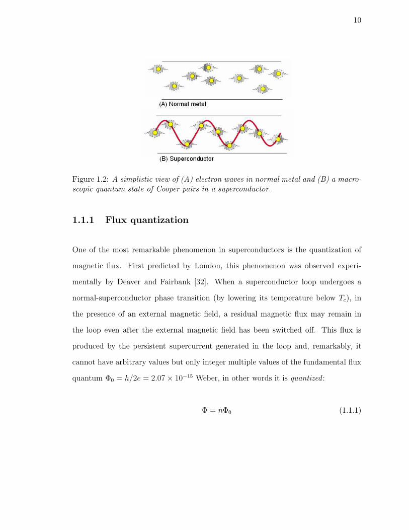
extending throughout the material, as shown schematically in figure 1.2. Cooper
pairs, hence, retain phase coherence over long distances, leading to interference and
diffraction phenomena. For more important theoretical details, see [8, 20].
10
Figure 1.2: A simplistic view of (A) electron waves in normal metal and (B) a macro-scopic quantum state of Cooper pairs in a superconductor.
1.1.1 Flux quantization
One of the most remarkable phenomenon in superconductors is the quantization of
magnetic flux. First predicted by London, this phenomenon was observed experi-
mentally by Deaver and Fairbank [32]. When a superconductor loop undergoes a
normal-superconductor phase transition (by lowering its temperature below Tc), in
the presence of an external magnetic field, a residual magnetic flux may remain in
the loop even after the external magnetic field has been switched off. This flux is
produced by the persistent supercurrent generated in the loop and, remarkably, it
cannot have arbitrary values but only integer multiple values of the fundamental flux
quantum Φ0 = h/2e = 2.07 × 10⁻¹⁵ Weber, in other words it is quantized :
Φ = nΦ0 (1.1.1)

11
where n is an integer.
The quantization of magnetic flux in a superconducting ring is a direct conse-
quence of the fact that the macroscopic wave function Ψ, describing the macroscopic
quantum state due to the condensation of Cooper pairs into a single state,
Ψ(~r, t) = |Ψ(~r, t)|eiϕ(~r,t) (1.1.2)
must be single-valued. This means that in the absence of applied magnetic fields, the
macroscopic superconducting phase ϕ(~r, t) takes the same value for all Cooper pairs
throughout the superconductor. However, in the case of loop threaded by a magnetic
flux, the phase around the loop changes by 2πn, where n is the number of enclosed
flux quanta.
When an external magnetic flux is applied, the condition of quantization is pre-
served in the loop: an extra amount of supercurrent, a screening current, is generated
in the loop to produce a magnetic flux so that the proper value of the total flux
corresponding to the quantization condition is restored.
1.1.2 The Josephson junction
When two superconductors are separated by a thin layer, which can be an insula-
tor, a normal conductor or a constriction, the superconductivity is weakened. Such
weak link is known as Josephson junction (JJ). A typical realization of a weak link
is a superconductor-insulator-superconductor (SIS) tunnel junction, consisting of two

12
superconducting films, separated by a very thin oxide layer, typically 1-2 nm thick.
The most commonly used superconductors are Nb and Pb and the critical current
density of these junctions may be in the range 103 − 104 A/cm2. Instead of a thin
oxide layer other materials may be used, for instance a normal metal, corresponding
to a superconductor-normal-superconductor (SNS) junction, in which the metal layer
can be thicker.
However, a new class of Josephson junction, specially suited for the high-Tc su-
perconductors, is based on the strong anisotropy of the high-Tc cuprates and involves
weak coupling between two superconducting grains with different orientations, the so
called grain boundary junctions (GBJs) [78, 52]. Due to a well defined grain bound-
ary in a bycristal substrate, the fabrication technology for this junction type is the
most reliable and successful currently appropriate for SQUIDs. A bycristal GBJ is
fabricated by the epitaxial growth of a high-Tc thin film on a bycristal substrate with
a predetermined misorientation angle θ (see figure 1.3). This method can be used to
obtain arbitrary misorientation angles and geometries, enabling a systematic study of
transport properties across high-Tc grain boundaries. The grain boundary is formed
along a straight line running across the substrate.
Actually, a wide variety of JJs have been used to fabricate SQUIDs. They fall into
three main classes: junction with intrinsic interface (grain boundary), extrinsic in-
terface (extrinsic barriers) and without interfaces (weakened structures). Here, we
have described the bycristal GBJs, since the SQUID sensor used in our SSM has been
fabricated with such technique. For more details and references on fabrication and

13
Figure 1.3: Sketch of the thin-film bicrystal principle using the example of a symmetric[001]-tilt grain boundary with a tilt angle θ.
properties of HTS JJs see [18].
1.1.3 The Josephson effect
If two superconducting regions are kept totally isolated from each other, the phases
of the electron-pairs in the two regions are uncorrelated. However, if the two regions
are brought together so that electron-pairs may tunnel across the barrier, the two
electron-pair wave functions will become coupled. This means, in practice, that a
supercurrent can flow in spite of the presence of the tunnel barrier as predicted by B.
D. Josephson and this phenomenon is known as Josephson tunneling [61].
Thus, a Josephson junction is a superconductor interrupted by a thin insulating
layer, where superconductive properties are weakened, as shown in figure 1.4. In the
Josephson formulation, the phase difference between two superconductors is a well
defined physical quantity and it obeys to the relation (dc Josephson effect)

14
Figure 1.4: A Josephson junction may be represented by a superconductor interruptedby a thin insulating layer. The applied current I controls the difference δ = ϕR −ϕL between the phases of the complex order parameters of the two superconductorsaccording to the dc Josephson’s relation (eq. 1.1.3).
Is = Ic sin(ϕ1 − ϕ2) (1.1.3)
Equation 1.1.3 describes the relationship between the supercurrent Is passing across
the junction, the difference between the phases ϕ1 and ϕ2 of the condensate states
in the two superconducting electrodes, and the critical current, Ic, i.e. the maximum
current which the junction can support without developing any voltage across it.
Furthermore, if a constant voltage V is maintained across the junction, the fol-
lowing relation (ac Josephson effect) predicts that
V =~
2e
d
dt(ϕ1 − ϕ2) (1.1.4)
the phase difference δ = ϕ1 − ϕ2 evolves linearly with time, i.e. ϕ = ϕ0 + 2e/~V t,
the Josephson current alternates with a frequency ν = 2eV/h = 483.6MHz/µV (ac
Josephson effect), and the junction behaves as a frequency-voltage transducer.

15
As the current across the junction is increased from zero, for I < Ic the phase
difference has the value δ = arcsin I/Ic constant in time, so that the voltage across
the junction remains zero (V = 0). When the current exceeds the critical current
I > Ic, the phase difference evolves according equation 1.1.4 and there is a voltage
across the junction (V 6= 0).
The relation between the current and the voltage for a Josephson junction is
represented by the I-V characteristic reported in figure 1.5 (A). The I-V curve shows
that if the junction is biased with a constant current source, lower than the critical
current Ic, there will be no voltage drop across the junction, although the passage
of the current through the device will introduce a phase difference across it. When
the bias current exceeds Ic, a voltage will appear and the phase difference become
time-dependent.
Figure 1.5: I-V characteristic: (A) non-hysteretic junction and (B) hysteretic junc-tion.
Just one year later the discovery of Josephson tunneling, Anderson and Rowell [4]

16
made the first observation of the dc Josephson effect, using a thin-film, Sn-SnOx-Pb
junction cooled in liquid helium. They showed that the current voltage characteristic
of a Josephson junction, owing to the capacitance associated with the structure, was
strongly hysteretic (see figure 1.5 (B)). This hysteresis can be eliminated by shunting
the Josephson junction by a normal ohmic resistor R. For dc SQUID realization,
one uses exclusively resistively shunted non hysteretic junctions with a single valued
current voltage characteristic.
Subsequently, Rowell [105] showed that a magnetic field B, applied in the plane
of the thin films, caused a modulation of the critical current according to the relation
Ic(Φ) = I0(0)|sin(πΦ/Φ0)
(πΦ/Φ0)| (1.1.5)
Thus, the critical current becomes zero for Φ equal to integer units of the flux quan-
tum Φ0 ≈ 2.07 × 10⁻¹⁵ Wb.
The observation of this Fraunhofer-like result, which is analogous to the diffraction of
monocromatic coherent light passing through a slit, is a validation of the sinusoidal
current phase relation.
Later, Jaklevic et al. [57] demonstrated quantum interference between two thin-
film Josephson junctions connected in parallel on a superconducting loop. The de-
pendence of the critical current on the applied magnetic field is shown in figure 1.6.
The rapid oscillations are due to the quantum interference between the two junc-
tions, whereas the slowly varying modulation arises from the diffraction-like effect of

17
Figure 1.6: Josephson current vs. magnetic field for two junctions in parallel showinginterference effects. (as reported in ref. [57]).
the two junctions. The period of oscillations is given by the field required to gener-
ate one flux quantum in the loop: thus, the maxima critical current occur at Φ/Φ0
= 0,±1,±2, ... ± n. The observations of these oscillations set the stage for the dc
SQUID. A useful reconstruction of the sequence of events and the motivations about
the discovery and the invention of the SQUID can be found in [110].

18
1.2 Superconducting Quantum Interference Devices
(SQUIDs)
Steaming the more mature technology, the first kind of dc SQUID was obviously a
low-Tc SQUID. First, the development of the planar dc SQUID with an integrated
multiturn input coil [66] and second, the invention of high reproducible Nb−AlOx−Nb
tunnel junction, ensured the robustness of most of the wafer devices.
However, the advent of high-Tc superconductivity in 1986 [12] resulted in the de-
velopment of new types of SQUIDs based on high-Tc thin-film technology [26, 28].
Indeed, the first routinely fabricated thin-film dc SQUIDs were made from YBCO
with grain boundary junctions, formed between randomly oriented grains in the film
[77]. To date, the majority of high-Tc SQUIDs are made with more controlled by-
cristal GBJs: a YBCO film is deposited on a bicrystal substrate of SrT iO3 or MgO in
which there is an in-plane misorientation of 24o or 30o. The films growth epitaxially
on the substrate, is subsequently patterned into two bridges few micrometers wide.
A configuration for bicrystal HTS dc SQUIDs is shown schematically in figure 1.7.
Adopting high-Tc SQUID technology, a major issue that was recognized early was
the prevalence of 1/f noise at low frequencies, that is, noise with power spectral
density scaling inversely with the frequency f . In fact, we may distinguish two inde-
pendent sources of such noise: one is correlated to critical current fluctuations and
the other one is produced by the uncorrelated hopping of flux vortices among pinning
sites in the films. Both noise mechanisms yields a 1/f power spectrum.
The level of flux noise was greatly reduced by the progressive improvement of film
quality, which lowered the density of pinning sites. The use of slots or holes in the film

19
Figure 1.7: Schematic presentation of a ”square washer” dc SQUID based on bicrystalJosephson junctions.
effectively reduced the generation of 1/f noise in devices cooled in weak fields [31].
On the other hand, for dc SQUIDs a modulation technique employing bias-current
reversal has proved to be very effective in averaging out this noise signal [80].
1.2.1 The dc SQUID
The dc SQUID is a magnetic flux-to-voltage transformer. It consists of two Joseph-
son junctions connected in parallel on a superconducting loop, as shown in figure 1.8.
When a symmetric dc SQUID is biased with an external dc current IB, a current I/2
flows through each of the two junctions; the critical current of the SQUID, or the
maximum current it can sustain without developing a voltage drop across it, in the
absence of any external magnetic fields, is thus 2Ic. When a magnetic flux is applied
perpendicular to the plane of the loop, the loop responds with a screening current J

20
Figure 1.8: Schematic representation of a dc SQUID. Two Josephson junctions (rep-resented by the two crosses) interrupt a superconductive loop. A bias current can befeeded in both junctions through the parallel connection. A dc SQUID is operated bybiasing the device at a constant current IB, a variation of the voltage V is achievedwhen the externally applied magnetic flux Φ changes. There are also shown the twoshunt resistances R and the capacitance C of each junction.
to satisfy the requirement of flux quantization
Φ = Φext + LJ = nΦ0 (1.2.1)
where L is the inductance of the loop and the total flux of equation 1.1.1 has been
explicitly expressed as an external contribution plus a screening contribution. Each
junction is resistively shunted to eliminate any hysteresis on the current-voltage char-
acteristic so that the latter appears as sketched in figure 1.9 (A).
The screening current J is zero when the applied external magnetic flux is an

21
Figure 1.9: (A) Schematic representation of a dc SQUID IV characteristic. Varyingexternally the applied magnetic flux, the IV curve will oscillate periodically betweentwo states: the integer Φ = nΦ0 and half integer flux Φ = (n + 1/2)Φ0. The twolimiting branches differ essentially for the maximum critical current. (B) dc SQUIDvoltage modulation measured at constant bias current as a function of the appliedmagnetic flux.
integer number of Φ0 and has a maximum value equal to ±(Φ0/2L), as derived by
equation (1.2.1), when the external flux is exactly between two integer values of Φ0,
i.e. when it is (n + 1/2)Φ0. Thus, J exhibits a periodic variation with the externally
applied magnetic flux. As the flux is increased above the value (n+1/2)Φ0, a transition
from the state n to n+1 takes place, corresponding to the entrance of a flux quantum
in the loop and J abruptly changes the sign, as shown schematically in figure 1.10
(A).
The effect of the screening current J flowing around the SQUID loop is the re-
duction of the critical current of the SQUID from 2Ic to (2Ic − 2J). In fact, this
circulating current adds and subtracts respectively itself to the bias current flowing
in the two branches of the loop containing the junctions, so that the critical current

22
Figure 1.10: Variation of (A) the screening current Js and (B) the maximum criticalcurrent as a function of the applied flux.
of the junction is reached when I/2 + J = Ic.
Thus the SQUID switches to the voltage state when I > Ic − 2J . Since J is a
periodic function of the externally applied flux, the critical current of the SQUID is
also a periodic function of the externally applied flux, as shown in figure 1.10 (B).
As a consequence of these considerations, if the SQUID is biased with a current
slightly larger than 2Ic, the output voltage of the SQUID turns out to be a periodic
function of the magnetic flux applied perpendicular to the plane of the SQUID loop,
as shown in figure 1.9 (B). The SQUID device thus works as a transducer of magnetic
flux producing measurable voltage, which changes its output for small changes of the
applied magnetic flux.
An important parameter characterizing the efficiency of this operation is the flux-
to-voltage transfer coefficient VΦ. In fact, the maximum response to a small flux
change δΦ ≪ Φ0 is obtained by choosing the bias current so that it maximizes the
amplitude of the voltage modulation and sets the external flux at Φa ≈ (2n+1)Φ0/4,

23
where the transfer coefficient VΦ = |(∂V/∂Φa)I | is a maximum. The resulting voltage
change ∂V = VΦ∂Φa is approximatively linear in this regime.
The maximum value VΦ can be obtained observing that, as the flux varies by
Φ0/2, the critical current variation is Φ0/L, and the corresponding voltage variation
is ∆V = (Φ0/L)R/2, where R/2 is the parallel resistance of the two shunts. This
gives the value VΦmax ≈ ∆V/(Φ0/2) ≈ R/L.
A very important issue in connection with the SQUID operation is the voltage
noise which affects the SQUID performances. Of course, one would keep noise as low
as possible. The major source of noise is related to the presence of shunt resistance
in the junctions constituting the SQUID. Resistors are universally affected by voltage
noise because of the thermal fluctuation of the electron density, the so called Nyquist
noise.
The Nyquist noise in the shunt resistors introduces a white voltage noise across the
SQUID with a spectral density SV (f), which turns into the flux noise spectral density
SΦ(f) = SV (f)/V 2Φ (1.2.2)
Since the latter parameter takes in count the dimension of the SQUID loop, it is often
useful to characterize SQUIDs in terms of their energy noise
ε(f) = SΦ(f)/2L (1.2.3)
Equation 1.2.3 is independent of the SQUID loop inductance L and the energy noise

24
becomes a good parameter to compare different SQUIDs and other magnetic sensors,
as it will be shown in chapter 2.
1.2.2 SQUID readout
Since the response of the SQUID is a periodic transfer function (see figure 1.9 (B)),
in order to linearize it, John Clarke et al. [27] came out with the idea of operating
the SQUID in a flux-locked loop (FLL).
Figure 1.11 shows a schematic of a dc SQUID operated by a FLL. An oscillator
applies a modulation flux at frequency fm (100 kHz signal) to the SQUID through a
feedback coil. The voltage signal of the SQUID, Vs, goes through a preamplifier, is
synchronously detected and then sent through an integrating circuit. The output of
the integrator is connected to the feedback coil through a resistor Rf .
When the flux in the SQUID is nΦ0, the V-Φ curve is symmetric about this local
minimum and the resulting voltage is a rectified sine wave, as shown in figure 1.12
(a), with a frequency double of fm. Thus the output of the lock-in detector is zero.
On the other hand, if the flux is shifted away slightly from the local minimum, the
voltage across the SQUID contains a component at frequency fm and there will be
an output from the lock-in detector. When flux is (n + 1/4)Φ0 (figure 1.12 (b)), the
voltage across the SQUID contains only the component at frequency fm and hence
the output from the lock-in detector is a maximum. Thus, as one increases the flux
from nΦ0 to (n + 1/4)Φ0, to output from the lock-in is steadily increases; if instead
we decrease the flux from nΦ0 to (n−1/4)Φ0, the output from the lock-in is negative
(figure 1.12 (c)). After integration, this signal is fed back as a current through a
25
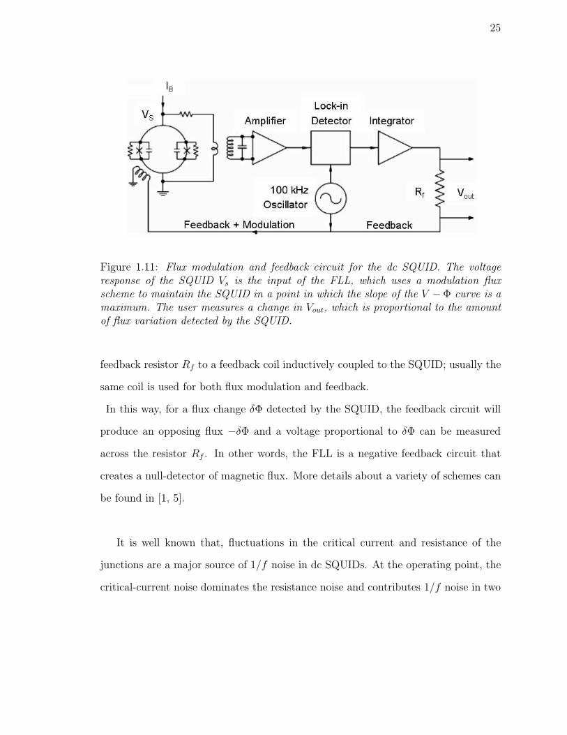
Figure 1.11: Flux modulation and feedback circuit for the dc SQUID. The voltageresponse of the SQUID Vs is the input of the FLL, which uses a modulation fluxscheme to maintain the SQUID in a point in which the slope of the V −Φ curve is amaximum. The user measures a change in Vout, which is proportional to the amountof flux variation detected by the SQUID.
feedback resistor Rf to a feedback coil inductively coupled to the SQUID; usually the
same coil is used for both flux modulation and feedback.
In this way, for a flux change δΦ detected by the SQUID, the feedback circuit will
produce an opposing flux −δΦ and a voltage proportional to δΦ can be measured
across the resistor Rf . In other words, the FLL is a negative feedback circuit that
creates a null-detector of magnetic flux. More details about a variety of schemes can
be found in [1, 5].
It is well known that, fluctuations in the critical current and resistance of the
junctions are a major source of 1/f noise in dc SQUIDs. At the operating point, the
critical-current noise dominates the resistance noise and contributes 1/f noise in two

26
Figure 1.12: Flux modulation scheme (as reported in [25]) showing voltage across thedc SQUID for (a) Φa = nΦ0 and (b) Φa = (n + 1/4)Φ0 , (c) the output VL from thelock-in detector versus Φa is shown.
ways. Fluctuations in the critical current, that are in-phase at the two junctions,
induce a voltage noise across the SQUID, that is eliminated by flux modulation at
frequency fm. Fluctuations, that are out-of-phase at the two junctions, are equivalent
to a flux noise that is not reduced by this scheme. Fortunately, this noise component
can be eliminated by means of several methods in which the bias current is period-
ically reversed [75, 37, 42]. These latter schemes are rarely implemented for low-Tc
SQUIDs where the cut-off frequency of the out of phase component of the critical
current 1/f noise is extremely low, but it is essential for high-Tc SQUIDs [33, 76]
where it is relatively high.
1.2.3 SQUID magnetometers
The previous description of a quantum interferometer is rather oversimplified. More
detailed analysis of a SQUID include the explicit dynamics of the two phases in the
presence of noise, asymmetries, etc. [115] so that the output voltage can be correctly

27
predicted as a function of the flux.
Moreover, to operate these structures efficiently as magnetic sensors requires the
introduction of a number of practical solutions which in the course of the years have
been recognized and reflect nowadays practical SQUID designs. Indeed, one of the
main issue is the area of the superconducting loop containing the junctions. To ensure
the largest possible flux change, being ∆Φ = As∆B, it appears advantageous to make
the loop area As as large as possible. On the other hand, we know that the modu-
lation depth of the maximum supercurrent decreases with increasing ring inductance
oscillating between 2Ic and 2Ic − Φ0/L. On the other hand, the inductance of the
loop is required to be as small as possible. Consequently, although the magnetic flux
noise SΦ(f) may be very low, the magnetic field noise SB(f) = SΦ(f)/A2s is often
too high for many applications. For this reason, most of applications require that
an additional superconductive loop structure is coupled to the SQUID to enhance its
magnetic field sensitivity.
Flux transformer
In order to avoid this problem and increase the effective area of the SQUID mag-
netometer, flux transformers are used [79]. A flux transformer is a closed supercon-
ducting loop in which the total magnetic flux is a constant. It is generally made by
two sections, as shown schematically in figure 1.13, a receiving end (pick up coil),
which can have several arrangements such as magnetometer, gradiometer etc. and a
coupling end (input coil), which can be coupled directly or inductively to the SQUID,
depending on technological and design requirements. If the external field through the
pick up coil changes, a shielding current is generated in the whole loop to compensate

28
the magnetic flux associated with the field change. The final effect is the generation
of a magnetic field in response to the magnetic field variation detected at the pick up
location.
Figure 1.13 (a) shows the configuration of a magnetometer, with a pick up loop
of inductance Lp connected to an input coil of inductance Li that is coupled to the
SQUID via a mutual inductance Mi = ki(LLi)1/2, where ki is a coupling coefficient.
Figure 1.13: Superconducting flux transformers: (a) magnetometers and (b) first-derivative axial gradiometer. The dashed box indicates a superconducting shield en-closing the SQUID.
The magnetic-field noise is
SB(f) = SΦ(f)/A2eff (1.2.4)
where Aeff is the effective area of the magnetometer. Clearly, one wants to make
Aeff as large as possible without increasing SΦ(f).

29
Washer SQUID
A way to increase the effective area of the SQUID without increasing its inductance
can be fulfilled owing to the thin-film technology and to the diamagnetic (the ability
to deviate magnetic field lines) properties of superconductors. Indeed, in the place
of a thin loop, one uses flat large area superconductors known as washer SQUID (see
figure 1.14) or Ketchen SQUID [66] from the name of the researcher who first intro-
duced this solution.
Figure 1.14: A washer SQUID. (a) Directly coupled magnetometer: the DC SQUID isconnected to the pick up loop. (b) a particular of the coupling between the SQUID andthe input coil. Dashed line indicates grain boundaries. (c) A picture of such devicemade by HTS group of CNR - Istituto di Cibernetica ”E. Caianiello” of Pozzuoli,Naples - Italy [101].
When a magnetic field is applied normally to the film plane, shielding currents flow
in the superconducting film. The screening currents, circulating around the inner gap
(∼ 10 µm for SQUID operated at 77K), essentially determine the superconducting
loop size of the SQUID and hence its inductance. The outer shielding currents con-
tribute to focus the field in the inner opening, increasing the collected flux. In this
condition, the effective area Aeff of the SQUID, may be reasonably approximated by
30
Dd, where d and D are the inner and outer dimensions of the washer, respectively.
It is worth noting that the outer diameter cannot be too large otherwise during the
cooling process, vortices start to be trapped into the structure hampering the normal
operation of the device.
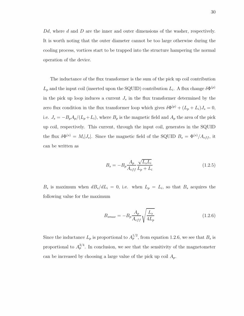
The inductance of the flux transformer is the sum of the pick up coil contribution
Lp and the input coil (inserted upon the SQUID) contribution Li. A flux change δΦ(p)
in the pick up loop induces a current Js in the flux transformer determined by the
zero flux condition in the flux transformer loop which gives δΦ(p) + (Lp + Li)Js = 0,
i.e. Js = −BpAp/(Lp +Li), where Bp is the magnetic field and Ap the area of the pick
up coil, respectively. This current, through the input coil, generates in the SQUID
the flux δΦ(s) = Mi|Js|. Since the magnetic field of the SQUID Bs = Φ(s)/Aeff , it
can be written as
Bs = −BpAp
Aeff
√LsLi
Lp + Li(1.2.5)
Bs is maximum when dBs/dLi = 0, i.e. when Lp = Li, so that Bs acquires the
following value for the maximum
Bsmax = −BpAp
Aeff
√
Ls
4Lp(1.2.6)
Since the inductance Lp is proportional to A1/2p , from equation 1.2.6, we see that Bs is
proportional to A3/4p . In conclusion, we see that the sensitivity of the magnetometer
can be increased by choosing a large value of the pick up coil Ap.

31
Moreover, the input coil is required to have an inductance matching with the pick-up
loop (Lp = Li), while remaining tightly coupled to the SQUID loop. As the size of
the pick-up loop is larger than the SQUID loop, to realize this matching the input
coil is laid over the SQUID washer as a multiturn thin-film spiral, separated from the
superconducting washer by an insulating layer.
This geometry has been adopted practically universally ever since its introduction
although some workers have based their design on other geometries such as the mul-
tiloop SQUID. This consists of several relatively large pick up loops all connected in
parallel across the same junctions to reduce the SQUID inductance. A comprehensive
theory for thin-film multiloop SQUIDs and their performance at 77 K has been given
by [38].

Chapter 2
Room-Temperature ScanningSQUID Microscope
Scanning SQUID microscope (SSM) is a Scanning Probe Microscope (SPM), where a
SQUID sensor is used to map the magnetic flux at a certain height above the surface
of the sample. The measurement after a scan operation yields a two-dimensional
image of the measured magnetic flux value, as a function of the relative sensor-to-
sample position. A SSM has the advantage to incorporate the most sensitive magnetic
flux detector (SQUID), although it has a modest spatial resolution compared with
the other common scanning magnetic microscope (MFM, SHPM, etc.). However, it
remains the most powerful technique for measuring the surface and sub-surface mag-
netic field distribution.
This chapter is dedicated to the description of the room-temperature sample Scan-
ning SQUID Microscope located at Istituto di Cibernetica of CNR of Pozzuoli, Naples
(Italy). In particular, a description of the system in terms of sensor characteristics
and system optimization is carried out. The most commonly used Scanning Probe
Magnetic Microscopes have been introduced in the first section. A brief overview of
32

33
the different approaches to Scanning SQUID Microscope design is reported in terms
of sample-temperature and SQUID sensors employed.
The second section is focalized on the description of the our Scanning SQUID Mi-
croscope and the strategies adopted to reduce the noise level system. Essentially two
main operational modes, alternating field (AC) or direct field (DC), are described.
Injection currents or alternating currents can be apply based on the sample charac-
teristics. A brief description of the lock-in technique used for the AC measurements
is also reported.
In the last section, the liquid nitrogen-cooled SQUID sensor used in our system
is described in terms of its configuration and magnetic noise performance. Spatial
resolution and field sensitivity have been calculated and some useful considerations
about our system performance have been reported.

34
2.1 Scanning Probe Magnetic Microscopy
Here we want to focus the attention on the many techniques for imaging local mag-
netic field or flux above a sample surface which are in use nowadays. Scanning
SQUID microscopy is one of the most powerful and promising techniques to measure
and image magnetic field distributions. This is mainly due to the SQUID unsurpassed
sensitivity, its linear and ability to operate without perturbing the sample, as well as
the versatility of the technique itself to measure a great variety of samples.
In addition to SSM, which is the subject of this thesis, widely used techniques
include decoration technique and magnetic-optical imaging, which are known for
their relative simplicity, and Scanning Electron Microscopy with Polarization Analysis
(SEMPA) [107], which can achieve high spatial resolution.
Moreover Magnetic Force Microscopy (MFM) [102, 54] can be used to combine
topographic and magnetic information. It measures the gradient of the magnetic field
and allows the imaging of very small magnetic structures of order of tens of nm. In
addition, the localized magnetic field from the MFM tip will change the micromag-
netic state of the sample which can complicate interpretations of the measurements.
On the other hand, its magnetic sensitivity is orders of magnitude lower than that of
SQUIDs.
Finally, Scanning Hall Probe Microscopy (SHPM) [96, 106] is a technique which
allows a good spatial resolution but shows a flux sensitivity lower than SQUIDs and
the sensor does not need to operate at low temperature. However, SQUIDs rapidly
become more sensitive than Hall bars with increasing pickup loop area. An interesting

35
review on such magnetic techniques can be found in [30].
A comparison between the spatial resolution and the magnetic field sensitivity of
different types of systems is shown in figure 2.1.
Figure 2.1: Comparison of the spatial resolution and magnetic sensitivities of differentmagnetic microscopy techniques.
.
However, each technique has its own advantages and disadvantages and the deci-
sion to use one versus the other one depends on several factors such as: sensitivity,
spatial resolution, frequency response, source-to-sensor distance, detection of fields
versus gradients, need to operate in an externally applied field, ability to reject ex-
ternal noise, ability to make measurements without perturbing the sample, and the
required operating temperatures of both the sample and the sensor.

36
2.1.1 Scanning SQUID Microscopy
Scanning SQUID systems can be used for the detection of weak magnetic fields gen-
erated, for instance, by electronic circuits or biological samples. Compared to other
magnetic evaluation methods for microscopic objects, the SMM has a higher magnetic
field sensitivity and high linearity over a wide dynamic range. The disadvantages of
this instrument are modest spatial resolution and the requirement for a cooled sensor.
Further improvement of the spatial resolution is possible using a better combination
of a smaller-sized SQUID pick-up loop and reduced distance to the object. By mini-
mizing SQUID-to-sample separation for higher field and spatial resolution represents
a problem for room temperature objects, which are placed outside the cryostat.
Here we describe a SMM for room temperature objects with a liquid nitrogen-
cooled SQUID sensor. Its capability to operate in magnetic fields up to about 5 G
allows to perform 2D mapping of the local dc and ac susceptibility of the objects.
2.1.2 Volumetric energy resolution
SQUID magnetometers show a optimal combination of field sensitivity and spatial
resolution compared with the other magnetic sensors. There are different parameters
used to compare magnetic sensors as reported in [39, 35], but the energy resolution
with respect to the sensor volume is proposed as a convenient way to compare high
sensitivity magnetic sensor, as reported in [103]. Such volumetric energy resolution
parameter is now defined as
ε(f) ≈ SΦ(f)
2L≈ SB(f)
2LΩ (2.1.1)

37
where SΦ(f) and SB(f) are the flux noise and magnetic field noise spectral density,
respectively, L is the pick-up coil SQUID inductance, and Ω is the sensor volume.
A comparison between SQUID and the recent advances in room temperature solid
state sensors, which include magnetoresistive devices (AMR, GMR, spin valve, and
spin dependent tunnelling device), giant magneto-inductive devices, atomic vapor
laser magnetometers, is shown in table 2.1.
Device Energy Resolution (J/Hz)SQUID w/pickup 1 × 10⁻³⁰
SERF 3 × 10⁻²⁹
Hybrid GMR/SC 4 × 10⁻²⁹
GMI 6 × 10⁻²⁸
AMR 7 × 10⁻²⁶
CSAM 2 × 10⁻²⁵
He4 4 × 10⁻²⁴
Fluxgate 3 × 10⁻²³
GMR w/feedback 4 × 10⁻²³
Hall 5 × 10⁻²³
Magnetoelectric 5 × 10⁻²³
TMR w/FC 1 × 10⁻¹⁹
Table 2.1: Comparison between different magnetic sensors by means of their energyresolution-to-volume [103].
It is possible to show that the sensor with the better spatial and magnetic resolution
is the one with the minimum value of ε(f). In the specific case, SQUID sensor, with
an energetic resolution of order of 10−30 J/Hz, is the device showing the best com-
promise between these two parameters, as it is presented in table 2.1.

38
2.1.3 Low-Tc and high-Tc SSM
In a scanning SQUID microscope the sample is scanned by a SQUID, which measures
the magnetic field above the sample surface. At present there are several different
approaches to design a scanning SQUID microscope, according to the sample tem-
perature (cold or room-temperature (RT)) and also the type of SQUID sensor (low or
high-Tc) used. These are well summarized by Kirtley and Wikswo in [69] and shown
in figure 2.2.
Figure 2.2: Various strategies have been used for scanning the sample relative to theSQUID, as reported in [69]. Both sample and sensor can be cooled (a-c) or only theSQUID (d-f). The field at the SQUID can be detected (a, d), or a superconductingpickup loop can be inductively coupled to the SQUID (b, e), or the pickup loop can beintegrated into the SQUID design (c). In (f), a ferromagnetic tip is used to coupleflux from a room temperature sample to a cooled SQUID.
.
Historically, low-Tc cold-sample SQUID microscope was the first to be developed

39
immediately after the invention of the SQUID magnetometer [122, 57]. The first two-
dimensional scanning SQUID microscope was invented by Rogers and Bermon [104].
They observed flux trapped in a superconducting niobium thin film. More recently,
low-Tc SQUID microscopy for cold samples has been extensively used to study a great
variety of superconducting phenomena: vortex trapped in a planar superconducting
film [72], Meissner imaging [73], phase-sensitive symmetry tests [74, 44], diamagnetic
shielding above Tc [56].
Black et al. introduced high-Tc SQUID microscopy to study cold samples with
a variety of techniques, including static magnetization [13], eddy currents [14], radio
frequency [15] and microwave imaging [16]. On the other hand, high-Tc SQUID mi-
croscopy for RT samples has been extensively developed by two groups: Wellstood
group at University of Maryland [119, 21, 22] and John Clarke group at University
of California, Berkeley [89, 88, 45].
For some applications, the higher operating temperatures of high-Tc SQUID mi-
croscopes provide an important advantage in comparison with low-Tc SQUID systems.
Indeed, the cryogenic as well as the shielding requirements are much less restrictive.
However, higher operating temperatures impose higher intrinsic noise levels. High-Tc
SQUIDs also suffer from excess of 1/f noise at low frequencies. Therefore, high-
Tc SQUIDs have not yet achieved the key combination of low-noise performance,
low-frequency sensitivity and high spatial resolution, as request for some kind of ap-
plications. Efforts to improve its spatial resolution by meas of a ferromagnetic flux
focusing tip [112, 99, 51] have been made over the last few years.

40
However, SSM for RT-samples has found an important area of development in
the field of non-destructive evaluation (NDE) [36, 63, 62, 64]. The sensitivity at low
frequencies allows them to work as eddy-current sensor with high depth resolution
to detect flaw on paramagnetic materials. In addition, SQUID wide dynamic range
make them suitable to image defects in ferromagnetic structures.

41
2.2 Scanning SQUID Microscope System Design
The microscope consists of a high-Tc dc SQUID sensor, placed in vacuum with a
self-adjusting standoff, close spaced liquid nitrogen dewar, XY scanning stage and a
computer control system. The microscope is mounted on actively damped platform,
which reduces the vibrations from the environment as well as the internal stepper
motor noises. Two µ-metal shields enclose the overall system to eliminate environ-
mental electromagnetic field noise, which could degrade the system performance. A
picture of the SMM out of the µ-metal shields is shown in figure 2.3.
Moreover, to reduce low-frequency noise signals, including 50 Hz line noise, low-pass
hardware and software filters are used. A laser profilometer, high-resolution camera
and a 1 µm precision z-axis positioning system allow to achieve a close positioning of
the sample under the sensor.
Intrinsic noise system
Since our SSM is a semi-commercial prototype system, it has required a series of tricks
to reduce its intrinsic noise level. When the sample is scanned under the SQUID sen-
sor and the computer records the SQUID response as a function of the XY position,
the movement of the stepper motors increases the environmental noise detected by
the sensor by about 10 times at 100 Hz, as shown in figure 2.4 by a measurements of
spectral density noise.
The moving mechanism is constituted by high precision stepper motors with a min-
imum step size of 12.5 µm and it is located inside the two µ-metal shields. For this

42
Figure 2.3: A photograph of the Scanning SQUID Microscope located at CNR - Istitutodi Cibernetica of Pozuuoli, Naples (Italy).
reason, the residual magnetization of the scanning table and the movement of the
drive mechanism can reduce the SQUID performance. Thus, we proposed to reduce
the noise due to the movement of the motors with a trick in the software control. In-
deed, during the measurement the sensor is moving along a XY path and the motors
are turned off when the sensor is fixed in a measurement position.
However, the noise due to a residual magnetization of the metallic parts, which
form the scanning table and the rotational mechanisms, is reduced at the end of the

43
10 100 1000 10000 10
100
Motor ON Motor OFF
S B
1/2 [
pT /H
z 1/2 ]
Frequency [Hz]
Figure 2.4: Magnetic field noise of the microscope SQUID sensor in two µ-metalshields when the motor are turned on or off.
measurements applying a background subtraction. In this way, the intrinsic peak-
to-peak noise we measured, obtained by subtraction of two subsequent background
measurements, was about 20 nT. We observed that it was a consequence of a resid-
ual magnetization of the sample-support due to a foregoing mechanical processing.
In figure 2.5, on the left is shown the magnetic signal due to the sample-support,
as it was supplied with the system. On the right, there is the magnetic signal of
the background without the sample-support. The residual magnetization we observe
is essentially due to the metallic parts of the rotational mechanism. Changing the
sample support with one completely nonmagnetic and not subjected to mechanical
working, the lowest intrinsic noise we measured was reduced by two orders of mag-
nitude, and it is now of about 0.2 - 0.3 nT. Magnetic signals lower than this value
cannot be distinguish by background noise.

44
−500
50−50
0
50
−1000
100200
(B)
X [mm]
sample−support
(A)
Y [mm]
B [n
T]
−50
0
50
−50
0
50
−100
0
100
200
X [mm]
background
Y [mm]
B [n
T]
Figure 2.5: Magnetic signal of sample-support due to foregoing mechanical processing(A) and after we substituted it with a nonmagnetic support (B).
2.2.1 DC and AC measurements
The Scanning SQUID Microscope has been widely and successfully applied to study
the basic physical properties of superconductor materials, such as the measurement
of flux quantization in high-Tc superconducting microdisk [50], vortices trapped in
YBCO thin-film [48, 70], observation of diamagnetic precursor to the Meissner state
above Tc in high-Tc cuprates [55], imaging half-integer Josephson vortices in high-Tc
YBCO grain boundaries [73], revealing antiferromagnetic ordering in arrays of super-
conducting π-rings [71], etc. [68, 116], and for the observation of domain structure in

45
magnetic materials, such as epitaxial thin film fabricated with growth temperature-
gradient method [67]. These systems usually use low-Tc SQUID as sensor, which
assures high magnetic field sensitivity only for low temperature samples.
However, there are prominent examples of successful applications of DC technique
for samples at room-temperature. These are, for example, the study of magnetic
properties of magnetic thin films [41, 47], detection of magnetic domain structures on
data storage media [46, 49], geological [11, 9] or biological samples [43, 10], ferrous
inclusions in aircraft turbine disks [114], few tiny (∼ 100µm) undesirable metallic or
magnetic contaminants (Fe, Co, Ni, etc.) in products for food and pharmaceutical
industry [36, 113, 111], and mechanical degradation of alloy steel caused by tensile
deformation or by fatigue cycles [65].
The ability of the sensor to operate with relatively high magnetic fields allowed
measurements of the dc and ac susceptibility of the microscopic objects. For this rea-
son, according to the type of measurement, we distinguish two different techniques:
alternating magnetic field (AC) and direct magnetic field (DC).
AC technique: it is actually used to detect surface and sub-surface defects in
paramagnetic samples. We can apply an alternating magnetic field essentially in two
different ways: injecting directly an AC current into the sample to find, for instance,
fault currents in electronic devices, or inducing an AC current (known as Eddy cur-
rents) by means of an induction coil to find subsurface defects in a paramagnetic
samples.

46
DC technique: it is used to measure the residual magnetization of ferromagnetic
samples or, alternatively, in the presence of an additional static magnetic field (DC
magnet ring) to enhance the magnetic response of paramagnetic and diamagnetic
samples. Such techniques are schematically reported in figure 2.6.
Figure 2.6: Schematic representation of DC and AC techniques performed with SSM.(A) A direct measurement of the residual magnetization above a ferromagnetic samplesurface. A magnet ring fixed on the bottom of the dewar can be used to enhance thesignal of paramagnetic or diamagnetic samples; (B) and (C) Alternating magneticfield measurements: injection current and induced current technique, respectively.

47
2.2.2 Lock-in technique
In the AC operational mode, a time-varying vertical magnetic field can be applied to
the sample at frequencies up to 1 kHz. The AC field option includes an AC field coil,
a filter-box, a control lock-in software for the excitation, and an imaging software to
display both in-phase and in-quadrature information.
The AC coil is wound around a 18.8 mm diameter bobbin located at the bottom
of the liquid nitrogen dewar, as shown in figure 2.7.
Figure 2.7: Bottom view of the dewar showing the excitation coil, for AC measure-ments, centered to the SQUID loop. In the inset is shown a front view of the circularinduction coil.
A lock-in technique is used for AC measurements. It provides a DC output propor-
tional to the AC signal under investigation [108]. A phase-sensitive detector (PSD),
making such AC to DC conversion, which is essentially a multiplier, forms the heart
of the instrument. It rectifies only the signal of interest, suppressing the effect of noise
or interfering components which may accompany such signal. However, the noise at
the input of the lock-in is not rectified, but it is returned at the output as an AC

48
fluctuation. This means that the desired signal response, now a DC level, can be
separated from the noise by means of a narrow low-pass filter.
A wire diagram describing the operational modes of the SSM is shown in figure
2.8. In this configuration, the SQUID electronic (iMag-303, Conductus) is directly
controlled by PC trough a GPIB card, the SQUID output and the filter box are con-
nected to BNC box, the data are acquired through an Analog-to Digital Acquisition
Card, and the XY stage position is connected to a motion control card.
Figure 2.8: DC and AC option SSM wiring diagram.

49
In our SSM the lock-in is implemented via software. In figure 2.9, the wiring diagram
for a software lock-in is shown. The excitation signal VL sin(ωt), a sinusoidal signal
with chosen amplitude and frequency, is sent to the induction coil via software, by
means of an output Digital-to-Analog Converter (DAC).
Figure 2.9: Wiring diagram used to implement the lock-in software. The signals of theSQUID and the reference are multiplied by an internally generated signals, in-phaseand out-of-phase with the excitation signal, respectively.
The SQUID output signal VS, coupled inductively to the pick-up of the SQUID, has
the same frequency of the excitation signal VL, but different phase. This signal is mul-
tiplied by 2 sin(ωt) and 2 cos(ωt), filtered and integrated, obtaining the ”in-phase”
and ”in-quadrature” portion of the SQUID signal, respectively
ℜ(VS) = 2∑
[sin(ωt) · VS sin(ωt + ϑS)] ≈ VS cos ϑS (2.2.1)

50
ℑ(VS) = 2∑
[cos(ωt) · VS sin(ωt + ϑS)] ≈ VS sin ϑS (2.2.2)
At the same time, a reference signal VR measured across a 330 Ω resistor in the fil-
ter box, is used to solve the uncertainty on the phase. It has the same frequency
of the excitation signal VL but different phase, not necessarily equal to the phase
of VS, so that the same algorithm has been applied to it. Again, it is multiplied
by 2 sin(ωt) and 2 cos(ωt), filtered and integrated, obtaining ℜ(VR) ≈ VR cos ϑR and
ℑ(VR) ≈ VR sin ϑR, respectively. Finally, the ratio between these two quantities gives
the measured complex signal VS
VRei(ϑS−ϑR), where VR is a known quantity. A descrip-
tion of how we use the in-phase and out-of-phase signals is widely dealt with in the
next chapter.

51
2.3 Scanning SQUID Microscope Sensor
In this work a semi-commercial Scanning Magnetic Microscope model 770 purchased
by Tristan Technologies, Inc. has been used. It utilizes high-Tc dc SQUID micro-
magnetometer, positioned to measure the vertical component of the magnetic field.
The SQUID structures were prepared from Y Ba2Cu3O7−x c-oriented films by a high
oxygen pressure dc-sputtering technique [100]. The measured magnetic flux-to-field
transfer coefficient of the SQUID is about 500 nT/Φ0, and the magnetic flux-to-
voltage transfer function is about 960 mV/Φ0. The estimated energy resolution value
for this sensor is 6.7 ·10−30 J/Hz in the white part of the noise spectrum.
The high-Tc SQUID is optimized for best compromise between spatial and mag-
netic field resolution, for operation at the liquid nitrogen temperature [40]. Sensitivity
and spatial resolution depend on the sensing area dimension and the sensor-to-sample
distance. The SQUID coil diameter δ is evaluated to be about 63 µm, which is the
parameter that more influence the ultimate system spatial resolution.
The SQUID is glued on the end of a sapphire rod which provides the thermal
contact of the SQUID assembly to the liquid nitrogen reservoir. The sensor is posi-
tioned in a Cu radiation shield and the SQUID-window standoff distance is fixed to
be several tens of µm. The SQUID is read out with commercial dc-SQUID electronics
(iMag Controller, Tristan Inc.) in a flux locked loop bias reversal mode [37].
The field resolution of the sensor was measured in shield and in unshielded laboratory
environment, as shown in figure 2.11. During the measurements the stepper motors

52
Figure 2.10: (A) Schematic view of the bottom dewar and SQUID location. (B)Optical image of the SQUID sensor. The inner diameter of the loop is about 63 µm.
of the positioning system were not connected. The white noise level is observed to
be the same for both spectra. The magnetic field white noise spectral density is 20
pT/Hz1/2 (measured at 5 kHz) and the operating bandwidth ranges from dc to 10
kHz. At frequencies below 100 Hz the signal spectrum shows 1/f noise knee, and the
unshielded sensor demonstrates mainly environmental noise.
In order to achieve the best spatial resolution, the SQUID must be positioned as
close as possible to the sample; a 50 µm thick sapphire window separates the sensor
from room temperature, allowing to operate at a sample-to-sensor distance of few
hundred microns. The effective distance between the sensor and the sample is ad-
justed through a laser beam. In order to calibrate the effective distance between the
sample and the pickup coil, a 150 mm long and 25 µm diameter straight copper wire
carrying a static current of I = 20 mA was scanned. The measured magnetic field

53
1 10 100 1000 10000 10
100
1000
10000
with shield without shield
Frequency [Hz]
S B
1/2 [
pT /H
z 1/2 ]
Figure 2.11: Magnetic filed noise of the microscope SQUID sensor in the presence oftwo µ-metal shields (red curve) and in unshielded condition (blue curve).
generated by the current in the wire is shown as cross-shaped dots in figure 2.12.
The solid line results from the data fit through the equation Bz(x, z0, I)
Bz(x, z0, I) =µoI
2π
x − x0
[(x − x0)2 + z20 ]
(2.3.1)
where I is the applied current, x0 is the location of the wire, z0 is the SQUID to
sample separation, and µ0 is the permeability of the vacuum.
The only free parameter used was the wire-to-coil spacing. For the shown data the fit
resulted in a wire to pickup coil distance of about ≈ 120 µm. The estimated separa-
tion value is in good agreement with the sum of the pickup coil-to-window distance,
the thickness of the sapphire window, and the sample-to-window spacing.

54
−20 −15 −10 −5 0 5 10 15 20−6
−4
−2
0
2
4
6x 10
−7
X [mm]
Bz [T
]
data fit
I = 20 mA
Figure 2.12: Magnetic field from a 150 mm long, 25 µm diameter thick, straightcopper wire carrying a current of 20 mA measured at a fixed height. The effectiveheight was determined to be 120 µm by fitting (solid line) the magnetic field datafrom a wire (cross-shaped dots).
2.3.1 Spatial Resolution and Magnetic Field Sensitivity
As it is well known, the sensitivity and spatial resolution depend both on the sen-
sor diameter and sensor-to-sample distance. Here, we compute them in terms of
dimensions of a simple SQUID magnetometer. The results can be useful to design,
characterize and optimize new magnetometers and to do some considerations about
our system performance.
Sensitivity
One way to compute sensitivity is to determine the minimum detectable magnetic
moment at a given location on the coil axis. Let us to consider a magnetic dipole of

55
moment mz oriented along the z-axis and positioned in the center of the pick-up coil,
as shown in figure 2.13
Figure 2.13: Magnetic field generated by a magnetic dipole oriented along the z-axisand coupled to the pick-up loop of a magnetometer.
The vector potential at position ~r (x, y, z) due to the magnetic moment ~m is
~A(~r) =µ0
4π
m(xj − yi)
r3(2.3.2)
where i and j are the unit vectors along the X and Y axes, respectively. The mag-
netic flux through the SQUID sensor Φc0 is calculated integrating the vector potential
along the closed loop of the circular sensor coil of radius rs positioned at a height D.
The integration gives [117]
Φc0 = µ0mr2s
2(D2 + r2s)
3/2(2.3.3)

56
Equation 2.3.3 can be used to estimate the smallest detectable magnetic moment
mmin by choosing Φc0 as the total instrument flux noise Φnoise =√
SΦ∆f . Therefore
we write
mmin =2(D2 + r2
s)Φnoise
µ0r2s
(2.3.4)
The equation 4.1.7 shows that the moment sensitivity is a function of the sensor size
rs, the sensor-to sample distance D, and the total flux noise Φnoise. This latter quan-
tity diverges for very small sensing area (rs −→ 0), due to the small effective area of
the sensor, and for very large SQUID sensors (rs −→ ∞), due to the annulment of
the magnetic moment flux through the loop. Deriving the equation 4.1.7, we obtain
the optimal condition for rs =√
2D.
Spatial resolution
It is defined as the smallest detectable change in position of a single magnetic source,
or the smallest detectable separation of multiple magnetic sources.
When the point magnetic dipole is scanned from the origin of the XY plane, along
the x-axis with a small displacement δ ≪ max(rs, D), the flux Φcδ becomes a complex
function, as calculated and reported in [2]. However, it is possible to obtain an analyt-
ical expression for the spatial resolution, defined as the least detectable displacement
δmin = Φnoise
µ0mG(rs, D)1/2 (2.3.5)

57
where G is a geometrical factor. Deriving the equation 4.1.8, we obtain the optimal
condition rs = 0.59D. However, δ shows an additional singularity at the critical point
rsc = 2D, where the worst resolution for a circular pick-up loop is obtained.
These considerations will be more incisive if we report on a graph the normalized
values of mmin and δmin as a function of the ratio between the sensor size rs and the
stand-off distance D, as shown in figure 2.14.
Figure 2.14: The normalized moment sensitivity and spatial resolution versus theratio between a circular-shaped sensor loop 2rs, and a sample-to-sensor distance D.The optimum size-to-distance ratios for moment sensitivity and spatial resolution are2rs/D = 2.82 and 1.2, respectively. The spatial resolution diverges at 2rs/D = 4.
In conclusion, the best condition for a high spatial resolution is reached when the
sensor standoff distance is about double than the diameter coil. This is well realized
in our SSM, where the SQUID diameter is about 63 µm, the standoff distance was
estimated to be about 120 µm, and the coil diameter is about 60 µm. By increasing

58
the stand-off distance, the spatial resolution of the system gets worse. On the other
hand, the worst critical condition for the spatial resolution (for D = rs/2) is never
realized in our SMM, because the radius of the pick up coil is always smaller than
the minimum standoff distance that could be realized.

Chapter 3
Eddy Current Non DestructiveAnalysis
The principle of eddy current non destructive analysis (NDA) is based on the measure-
ment of induced eddy currents in conducting objects, in the presence of time-varying
magnetic fields. In general, electromagnetic problems can be usually divided into
three categories: low frequencies, intermediate frequencies and high frequencies. At
low frequencies static conditions are assumed; at high frequencies wave equations are
used. However, in the intermediate frequency range, where diffusion equations are
used, very few problems have been analytically solved. Eddy current problems fall
into this intermediate frequency region.
The first section of this chapter is dedicate to the state-of-art of the eddy cur-
rent analysis in terms of penetration depth and current distribution. Fundamental
diffusion equation to eddy current problem is shown starting from the Maxwell’s equa-
tions. An analytical solution of Eddy current distribution is presented for a linear,
homogeneous and flawless conducting sample.
59
60
The second section is entirely dedicated to find novel analytical solutions to eddy
current problem in presence of sample with defects. Here, eddy current magnetic
field distribution as a function of the sensor position is derived in the case of a ”thin”
conducting plate. In this assumption, the induced magnetic field may be considered
uniform along the sample thickness. Such innovative theoretical approach is used to
analyze the acquired data of AC NDA technique.
In the last section, the capability and advantages of NDA systems based on Scan-
ning SQUID Microscope has been exploited, focusing on the analysis of damage in
joined metallic structures of aeronautical interest. A complete description of the AC
signals (”in-phase” and ”out-of-phase” components) is carried out. A phase rotation
analysis, based on the principle of phase variation for defects at different depths,
is performed to distinguish hidden defect signals enhancing their signatures. This
analysis is widely discussed and corroborated by a series of experimental results on
multi-layer metallic structures.

61
3.1 Eddy Currents
The principle of SQUID eddy current nondestructive analysis is based on the mea-
surement of induced eddy currents in conducting materials when they are subject
to time-varying magnetic fields BExcitation, as shown in figure 3.1. The eddy current
distribution in a metal (and its associated magnetic field BEddy) is disturbed when
the eddy currents are induced in a region containing defects, like flaws or cracks. The
presence of a flaw in conducting plates can be detected by measuring the change in
BEddy as the sensor moves from a flawless region to that containing a flaw.
Figure 3.1: Schematic representation of the primary and secondary magnetic field..
Eddy currents are closed loops of induced current circulating in planes perpendicular
to the magnetic flux. They normally travel parallel to the coil’s winding and flow is
limited to the area of the inducing magnetic field. Eddy currents concentrate near the
62
surface adjacent to the excitation coil and their strength decreases with distance from
the coil. Eddy current density decreases exponentially with depth. This phenomenon
is known as the skin effect.
The skin effect arises when the eddy currents flowing in the test object at any
depth produce magnetic fields which oppose the primary field, thus reducing the net
magnetic flux and causing a decrease in current flow as the depth increases. Alterna-
tively, eddy currents near the surface can be viewed as shielding the coil’s magnetic
field, thereby weakening the magnetic field at greater depths and reducing induced
currents. The depth that eddy currents penetrate into a material is affected by the
frequency of the excitation current, electrical conductivity, and magnetic permeability
of the specimen, as shown in the figure 3.2. In particular, it decreases with increasing
frequency, conductivity, and magnetic permeability.
The depth at which eddy current density has decreased to 1/e, or about 37% of the
surface density, is called the standard depth of penetration δ defined as
δ =
√
1
πµσf(3.1.1)
where f [Hz] is the test frequency, µ [H/m] is the magnetic permeability of the material
and σ [S/m] is its conductivity. Although eddy currents penetrate deeper than one
standard depth of penetration, they decrease rapidly with depth. At two standard
depths of penetration 2δ, eddy current density has decreased to 1/e squared or 13.5%
of the surface density. At three depths 3δ the eddy current density is down to only
5% of the surface density.

63
Figure 3.2: Penetration depth as a function of excitation frequency, conductivity, andpermeability of the sample.
To date, many papers dealing with both theoretical and practical aspects of eddy
current testing of materials have been produced [120, 36, 60, 19, 82]. The theo-
retical analysis for the eddy-current problem is important for the quantitative non-
destructive evaluation. Till now, analytical solutions for the eddy current distribu-
tions have been studied for the unflawed samples excited by a sheet inducer [92] and
a circular excitation coil [34, 29].
However, for flawed conducting samples, it is difficult to obtain the analytical for-
mula for eddy-current distribution because of complex boundary conditions imposed
by the presence of the flaw. For this reason, many authors investigate numerically
the eddy-current distribution in a conducting sample with a flaw by using a Finite
Element Method (FEM) [97, 86, 58, 24].

64
3.2 Mathematical Derivation of Eddy Currents
For the calculations in this work, it was assumed that the excitation field generated
by the circular coil is less than few MHz, so that the displacement term in Maxwell’s
equations can be neglected. In addition, the sample was assumed to be non-magnetic
with permeability µ = µ0. A current carrying coil will give rise a magnetic field
according to the Ampere’s equation:
∇× H = J (3.2.1)
H can be written in terms of vector potential,
∇×A = µH (3.2.2)
Substituting Eq (3.2.2) into Eq (3.2.1),
∇×∇× A = µJ (3.2.3)
and remember the identity ∇×∇×A = ∇· (∇·A)−∇2A, with ∇·A = 0, we obtain
∇2A = −µJ (3.2.4)
where the total current J is given by the superposition of the current source and eddy
current contribution:

65
J = σE + Jsource (3.2.5)
As a consequence, the Eq (3.2.4) can be written:
∇2A = −µσE − µJsource (3.2.6)
Using the Faraday’s equation:
∇× E = −∂B/∂t (3.2.7)
B can be written in terms of vector potential:
B = ∇× A (3.2.8)
Substituting Eq (3.2.8) into Eq (3.2.7), we obtain the relation:
∇× (E + ∂A/∂t) = 0 (3.2.9)
that written in terms of the scalar potential φ becomes:
E + ∂A/∂t = ∇φ (3.2.10)

66
In the approximation of absence of free charge, the scalar potential can be chosen
equal to zero, so that Eq (3.2.10) becomes:
E = −∂A/∂t (3.2.11)
Finally, substituting the Eq (3.2.11) into Eq (3.2.6) we obtain the vector potential
diffusion equation
∇2A = µσ∂A/∂t − µJsource (3.2.12)
The Eq (3.2.12) is fundamental to understand the NDE techniques based on eddy-
currents. For time harmonic fields, E = −∂A/∂t = −ωA, so that Eq (3.2.4) becomes
∇2A = ωσµA− µJsource (3.2.13)
Here, A is the magnetic vector potential, µ the magnetic permeability, Jsource the
current flowing through the excitation coil, σ the electrical conductivity and ω the
frequency of the current flowing through the excitation coil, and =√−1. The first
term on the right-hand side of Eq (3.2.13) represents the induced eddy currents.
In analogy to the diffusion equation (3.2.12), the same relations for E, J and H
can be written:

67
∇2E = µσ∂E/∂t (3.2.14)
∇2J = µσ∂J/∂t (3.2.15)
∇2H = µσ∂H/∂t (3.2.16)
3.2.1 Penetration Depth
It is well know in NDE technique, that the sensitivity of flaw detection is decreased
by raising the operation frequency.
In this section, we show how to calculate the penetration depth on a conductor of
semi-infinite extension starting from the magnetic field diffusion equation reported
previously.
If we consider a semi-infinite conductor and a time harmonic excitation field ap-
plied in the x direction, Hx = H0eωt, the diffusion equation (3.2.16) becomes:
∂2Hx(z, t)
∂z2= µσ
∂Hx(z, t)
∂t(3.2.17)
Assuming Hx(z, t) = h(z)eωt and substituting into Eq (3.2.17), h(z) has to satisfy
the equation:
∂2h(z)
∂z2− ωµσh(z) = 0 (3.2.18)

68
If we choose h(z) = e−kz as particular solution of Eq (3.2.18) with k to be deter-
mined, we find k2 = −ωσµ and so:
k = ∓( − 1)
√
ωµσ
2(3.2.19)
Since k has the dimension of a length, we can obtain an expression for the skin depth
δ defined as:
δ =1
k=
√
2
ωµσ(3.2.20)
Hence, the skin depth effect limits the maximum depth of detection for any partic-
ular flaw size. The skin depth can be increased by lowering the operating frequency
and therefore the typical dc to kHz bandwidth of the SQUID is a real advantage for
SQUID NDE in the detection of subsurface flaws in conducting structures.
3.2.2 Eddy Current Distribution
In this section we find an expression for eddy current distribution as a function of δ
and the depth z measured from the surface of conducting sample. Using the expres-
sion (3.2.19) found for k, we can write the solution of Eq (3.2.17) as:
Hx(z, t) = C1e−z/δe(ωt−z/δ) + C2e
z/δe(ωt+z/δ) (3.2.21)

69
To determine the constants, we derive Hx = 0 and C2 = 0 for z → ∞ and at the
sample surface Hx = H0e−ωt and C1 = H0, for z = 0.
Finally, by substituting the constants C1 and C2, the solution of Eq (3.2.17) can
be written as
Hx(z, t) = H0e−z/δe(ωt−z/δ) (3.2.22)
At the surface of the sample, the generated magnetic field has the same time de-
pendence as the source current. However, as the magnetic field penetrates into
the sample, because of the finite conductivity of the sample a phase-lag result and,
Hx ∼ H0e(ωt−z/δ), where the term −z/δ takes into account the penetration depth.
If we choose to express the real component of the magnetic field, we can write:
Hx(z, t) = H0e−z/δ cos(ωt − z/δ) (3.2.23)
where δ is the given by (2/µωσ)1/2. The first term on the right side, e−z/δ, de-
scribes the penetration of the magnetic field in the medium, whereas the second term
cos(ωt− z/δ) represents the wave propagation.
Consequently, using the Ampere’s law J = ∇× H, we calculate the current dis-
tribution into our medium induced by a time-varying applied magnetic field. These
currents are referred to as eddy currents, due to their similarity with the eddies in
river water. Thus, deriving Eq (3.2.22), we observe that only the current component

70
in the y direction Jy is different from zero:
∇× H = ∂Hx(z, t)
∂z= Jy (3.2.24)
finally, we obtain an expression for the induced current, as follows:
Jy =H0
δe−z/δ[e(ωt−z/δ−π
2) − e(ωt−z/δ)] (3.2.25)
In qualitative terms, the eddy currents are out of phase with the inducing field,
proportional to the frequency of the applied field, and flow to oppose the changes in
the applied field with time.
As done previously, arranging the Eq (3.2.25), we can express the real component
of the induced current as:
Jy = −√
2H0
δe−z/δ cos(ωt− z/δ + π/4) (3.2.26)
The phase of the eddy current with respect to the excitation field is given by −z/δ +
π/4. The sign minus indicates that the induced currents generate a magnetic field
which opposes itself to the applied field with time.
This approach has been possible because we have supposed an applied magnetic
field Hx = f(z, t) and so, we were able to solve directly the diffusion equation (3.2.16)
for the magnetic field. In this contest, Dodd and Deeds [34] in 1968 found an ana-
lytical solution to eddy current problem with excitation coil located above plates of

71
various thickness, when a sinusoidal driving currents and linear, isotropic, and ho-
mogeneous media was assumed. This ”closed-form” solution was obtained for two
different conductor geometries and with the assumption of cylindrical symmetry.
More in general, for this electromagnetic problems, most people typically solve
numerically the diffusion equation for the vector potential A (Eq 3.2.12).
When there is a defect in the plate, the eddy current distribution around the the
flaw gets distorted. This modified distribution can be thought as a sum of the unper-
turbed distribution and a local perturbed distribution. The magnetic field associated
with such a modified distribution is the defect magnetic field. Therefore, its phase
φ(z) should also scale as −z/δ, where z is now the depth of the flaw from the top of
the plate. The linear relationship between the phase of the magnetic field generated
by the defect and the flaw depth is in agreement with experiments with both the
double-D [58, 59] and the sheet inducer excitation geometries [92]. The phase φ is
also equal to tan−1(B90o/B0o), where B0o and B90o are the in-phase and in quadrature
magnetic field components of the defect.

72
3.3 Eddy Current in Thin Conducting Plates
Another case can be solved analytically is when the thickness of the sample is neg-
ligible respect to the penetration depth δ. This condition is well carried out in low
frequency regime. In this assumption, if we consider an external time-varying mag-
netic field H(0)z , applied normally to the plate, we can observe that the component of
the applied magnetic field in the z direction is only a function of the variables (x, y)
on the plane and is independent of z.
The induced eddy current in the plate is defined by the curl of the z component
Hz(x, y, t) of the magnetic field:
J = ∇× (Hzk) = −k ×∇Hz (3.3.1)
and expressing the previous relation in terms of the field components, it becomes:
J = −k × (i∂Hz
∂x+
∂Hz
∂y) = i
∂Hz
∂y−
∂Hz
∂x(3.3.2)
The Eq (3.3.2) guarantees that the induced current J has only the two in-plane
components, Jx = ∂Hz/∂y and Jy = −∂Hz/∂x, respectively.
The governing diffusion equation (3.2.16) for Hz(x, y, t), becomes:
∂2Hz
∂x2+
∂2Hz
∂y2= µσ
∂Hz
∂t(3.3.3)

73
3.3.1 Magnetic Field Distribution in a flawed plate
Equation (3.3.3) could be solved analytically, as done for the Eq (3.2.17), in the
assumption of flawless thin conducting plate. More interesting, it would be to find
a solution to eddy current problem when there is a flaw in the sample and thus,
when the cylindrical symmetry is no longer valid. Nevertheless, we have derived an
analytical solution in the case of ”thin” flawed conducting plate. In this assumption,
we can neglect the variation of the magnetic field along the thickness of the sample.
As a simple case, we consider a thin conducting plate with a defect of circular
shape of radius a and we assume that the plate is large enough to neglect the border
effects, as shown schematically in figure 3.3.
Figure 3.3: A circular flaw of radius a is positioned in the center of the plate and inthe origin of the reference system. The circular induction coil is located on the plateand the projection of its center has coordinates (c1, c2).
The magnetic field in the Eq. (3.3.3) can be written as the sum of two compo-
nents, Hz = H(0)z +H
(1)z , where H
(1)z is the self-magnetic field due to the eddy current
J in the plate. Substituting this relation in the equation 3.3.3 and observing that for

74
the external magnetic field H(0)z is ∇2
xyH(0)z = 0, we obtain
∂2H(1)z
∂x2+
∂2H(1)z
∂y2= µσ
∂H(0)z
∂t+ µσ
∂H(1)z
∂t(3.3.4)
Neglecting the time dependence of the self-magnetic field H(1)z with respect to the
applied field H(0)z , the Eq (3.3.4) becomes
∂2H(1)z
∂x2+
∂2H(1)z
∂y2= µσ
∂H(0)z
∂t(3.3.5)
In addition, we chose an harmonic time dependence for the applied magnetic field,
i. e. H(0)z = H0e
ωt. We assume that H0 has a constant value in a circular region
of radius R under the coil and it is zero outside. If the solution of the Eq (3.3.5) is
assumed to be H(1)z (x, y, t) = Hz(x, y)eωt, we finally obtain:
∂2Hz(x, y)
∂x2+
∂2Hz(x, y)
∂y2= ωµσH0 (3.3.6)
The boundary condition requires that the current on the border of the defect has only
a tangential component. This condition is equivalent to the requirement that Hz is
equal to a constant on the border of the defect. More in general, Hz(x, y) = const.
determines the current density flux line family.
It is possible to show [6] that the solution to Eq (3.3.6), satisfying the required
boundary condition, is the following:

75
Hz − Hcenterz =
H0
δ2[(x − c1)
2 + (y − c2)2 − c2
1 − c22] ×
(1 − a2
x2 + y2) +
H0
δ2(c2
1 + c22 − a2); with x2 + y2 ≥ a2 (3.3.7)
As stated above, we assumed that an uniform applied magnetic field H(0)z extends
over a circular area of the plate having radius R. The constants (c1, c2), appearing in
the solution 3.3.7, are just the coordinates of the center of this circle on the plate. In
this point, the field is denoted as Hcenterz ≡ Hz(c1, c2).
This solution is shown in figure 3.4, where the lines represent the magnetic field
distribution on the plate around the defect, which are obtained for constant values
of the level curves Hz(x, y)− Hcenterz extending to a circular region of radius R. This
solution can be calculated for each point on the horizontal scanning position.
3.3.2 Eddy Current Density in the plate
Knowing the spatial variation of the magnetic field on the plate Hz(x, y) from Eq
(3.3.7), we can derive the expression for the magnetic field Hz(x, y, t) = Hz(x, y)ejωt.
Since the current density is equal to the curl of the magnetic filed , we can calculate
the components of the eddy current density excited in the plate, namely:
Jx =H0
δ2
[
2y − (2a2y) (2c1x + 2c2y)
(x2 + y2)2 − c2
(
2 − 2a2
x2 + y2
)]
ej(ωt+π/2)
(3.3.8)
Jy =H0
δ2
[
−2x +(2a2x) (2c1x + 2c2y)
(x2 + y2)2+ c1
(
2 − 2a2
x2 + y2
)]
ej(ωt+π/2)

76
-2 -1 0 1 2
-2
-1
0
1
2
x- coordinate
y-
coor
dina
te
Figure 3.4: A representation of the magnetic field distribution around the defect ob-tained by plotting the level curves of the magnetic field z component, Hz − Hcenter
z =const, as solution of the Eq 3.3.7. The flaw of radius a is in the origin of the referencesystem (0, 0) and the exciting coil center in this frame is positioned at (-1, 0). Thelinear increment of the current starting from the coil center is visible.
We can observe that in the absence of flaw (a = 0), the current density represented
by this solution varies linearly from the point (c1, c2) on the plate, corresponding to
the center of the coil of an arbitrary radius R, which we consider as the extension of
the eddy current on the plate. Moreover, this linear current behavior is related to the
choice of an uniform normal field generated by the coil in the circular area of radius R.

77
3.3.3 Eddy Current Magnetic Field at the sensor position
However, we are interested to measure the magnetic field at the sensor position. In
general, the magnetic field B(~r) at point ~r is given by the law of Biot and Savart
H =1
4π
∫
J(r′) × (r − r′)
|r − r′|3 dr′ (3.3.9)
where J is the current density at point ~r′.
In our case, since the sensor we used measures the z-component of the magnetic
field, we choose to calculate only Hz given by
Hz =d
4π
∫ ∫
Jx(x′, y′)(y − y′) − Jy(x
′, y′)(x − x′)
[(x − x′)2 + (y − y′)2 + z2]3/2dx′dy′ (3.3.10)
where d is the thickness of the plate and z is the sensor to plate distance.
The signal detected by the sensor, when the defect is moving along the x-axis
under the SQUID, can be calculated by evaluating the integral (3.3.10) over a cycle,
in which the value of c2 is fixed to zero and c1 is incremented of an arbitrary step.
This is equivalent to move the exciting coil over the flaw, as done in the simulating
program. The results of this procedure are reported in figure 3.5, where the magnetic
field at sensor position generated by a circular defect of radius a = 1 is calculated
for different z distances. Each dimensions used in the simulations are normalized in
terms of the skin depth δ.
Although the magnetic field signals, calculated through Eq (3.3.10) has an amount
of uncertainty due to the introduced approximations, the results we obtained are in

78
-7 -6 -5 -4 -3 -2 -1 0 1 2 3 4 5 6 7
1.00
1.01
1.02
1.03
1.04
1.05
1.06
1.07
z = 1
z = 0.5
z = 0.25
z = 0.1
Nor
mal
ized
Mag
netic
Sig
nal
Horizontal Displacement
R = 20 a = 1
Figure 3.5: Scan simulations of magnetic field recorded as a function of the horizontalposition above a circular defect of radius a. The value used for the area of interestfor the eddy current is R = 20. The curves correspond to different scanning quotes:z varies from 0.1 to 1 in units of δ. Each value must be meant as normalized withrespect to the skin depth δ.
qualitative good agreement with the experiment. This characteristic behavior shows
two peaks, when the center of the induction coil is just above the border defect,
and a valley when it is exactly on the center of the defect. Increasing the distance
sensor-to-defect, the signature of peaks and valley becomes less intensive.
This result will be reminded in the following section, to compare it with the
experimental eddy current data, detected above a circular defect of 4.5 mm diameter
in a thin conducting plate.

79
3.4 Scanning SQUID Microscope for NDE Appli-
cations
Various non-destructive testing (NDT) techniques, such as ultrasonics, radiography,
penetrants, magnetics, eddy currents and acoustic emissions have been tested to
determine the integrity of the structure, component or material as requirement in
both quality control for manufacturing processes and traditional flaw detection. The
choice of the NDT industry for an appropriate NDT method focuses on an optimum
balance between quality control and cost effectiveness.
Because of its higher costs and handling inconvenience, SQUID technology might
be used only where standard NDT techniques fail to ensure sufficiently high reliabil-
ity. The conventional eddy current techniques are sensitive in detecting the surface-
breaking cracks. However, these methods are not sensitive enough for the detection
of deep flaws due to their poor resolution at low frequencies.
One of the most important advantages to use a SQUID system is exactly the high
field sensitivity at low frequencies which provides an outstanding dynamic range with
remarkably high signal to noise ratio of the measured field distribution. This charac-
teristic offers an advantage for application where low excitation frequency is necessary
for detection at large penetration depth in multilayer structures, rivet plates and air-
craft wheels [63, 94, 85, 84, 83, 3, 81].
In SQUID-based NDE systems, the sample is excited with an ac excitation field
and the magnetic signal due to the generated eddy currents in the plate is measured.
Typical excitation field devices are sheet inducers, absolute coil exciters and differen-
tial double-D coils, as reported by Braginski and Krause [19] and schematically shown

80
in figure 3.6.
Figure 3.6: Typical configurations of inducer coils as reported by Braginski and Krause[19]: (a) to (c) Differential double-D coils with (a) axial gradiometer in plane, (b) ax-ial gradiometer normal to plane, (c) planar gradiometer; (d) and (e) absolute exciterswith planar gradiometer (d) and magnetometer (e); (f) sheet inducer.
The change of field response can be regarded as a function of a series of parameters
as reported [19] and shown in figure 3.7, respectively. The defect magnetic field can
be regarded as consisting of different components, as explained in [82]:
the surface current density,
the exponential decay of the excitation field, governed by a decay coefficient −z/δ,
the interaction process of the current density with the flaw
the decay of the return field.
Many efforts have been made to find a correlation between the magnetic signal
due to a flaw and the investigation of its dimension and depth. Yu Pei Ma and John
Wikswo [92], using a sheet inducer, demonstrated that the analysis of the phase of the
magnetic signal provides useful information about the depth of the flaw. In fact, it is
well know that there is a relationship between the phase of the magnetic signal and
the depth of the flaw due to the skin effect. It was found that for a fixed excitation
frequency, the phase of the measured signal varies linearly to the depth of the slot,

81
Figure 3.7: Typical important parameters in NDE testing as reported by Braginskiand Krause [19]: d - flaw diameter or size, z - flaw depth, h - sensor to flaw distance,a - separation of inducer above test object surface or stand-off distance, δ - skin depth.
while the amplitude is correlated with the the height of the slot [59, 58, 53].
As in other NDE fields, imaging technique are useful to facilitate the interpreta-
tion of measurement data obtained by SQUID magnetometry. There are essentially
two different approaches for processing of SQUID NDE data: flaw detection and field
deconvolution into current patterns. In this work, we want to emphasize the flaw
detection.
To this aim, we utilized a circular coil to characterize defects in conducting plates
at different depths. We show that the components of the measured signal are useful in
determining buried flaws in according with the high sensitivity of the SQUID system.
Hence, quantitative evaluation of flaws can be achieved by analyzing the amplitude
and the phase of the measured signals, in according with the experimental data. More
in particular, we focalize the attention on a particular application of crack detection
in aircraft components.

82
3.4.1 The Signal Components
Using the lock-in technique, for which more accurate description we refer to the lock-in
paragraph in chapter 2, the SQUID signal and the reference signal are multiplied. The
result after that the signal passes through a low pass filter is a dc signal proportional to
the amplitude of the signal coming from the sample and the cosine of the phase angle
between the SQUID and the reference signals, namely 12VsVL cos θs. To obtain phase
information, the reference signal is also connected to a 90o phase shifter. Multiplying
again the SQUID signal and the reference signal shifted by 90o, we obtain again a dc
signal 12VsVL sin θs.
Since VL is the amplitude of the reference signal and it is known, we can define two
quantities: B0o = Vs cos θ and B90o = Vs sin θ. These are, respectively, the ”in-phase”
or real and ”in-quadrature” or imaginary portions of the signal. Thus, two data fields
are typically recorded during each scan and together they represent the complex
response of the sample.
To probe the dependence of the excited magnetic field from the crack in a sample
and to show how it can be used to detect buried defects, as first simple case, we
considered an aluminium plate with a circular defect. The geometry of the simulated
flawed sample is shown in figure 3.8. The circular defect has a diameter of 4.5 mm and
the thickness of the plate is 3 mm. The circular coil, which is 18.8 mm in diameter, is
fed with 0.4 V at 889 Hz excitation frequency generating the applied magnetic field.
When the coil scans over the slot, the in-phase B0o and in-quadrature B90o com-
ponents of the excited magnetic field are recorded as a function of the horizontal
position, as shown in figure 3.9, and they are found to oscillate up-and-down.

83
Figure 3.8: A schematic description of the lock-in technique: the SQUID and thereference signals are multiplied and filtered through a low-pass filter. The result aretwo dc signal ”in-phase” and ”in-quadrature” with the inducing signal. The sample,an aluminium plate with a circular defect 4.5 mm in diameter, moves under the sensorin the x-direction.
At position a or c of figure 3.9, the real and imaginary components show a large
variation since the center of the circular coil is just above the slot. As a consequence
of their phase shift, B0o and B90o show a maximum and a flex in the points a and
c, respectively. At point b, the center of the circular coil is exactly in the middle of
the slot, and the two components of the signal show a coincident valley or a peak,
respectively.
The magnetic field component, in-phase with the inducing field, shows the behav-
ior we found in our simulation (see figure 3.5), with a valley when the the center of
the coil is exactly above the slot (position b), and two peaks when the center coil is
just above the slot (positions a and c).
We may solve these two signals for the magnitude, VS =√
B20o + B2
90o , and phase,

84
−30 −20 −10 0 10 20 3030−10
−5
0
5
10
Real B0°
Horizontal displacement [mm]
B [n
T]
−30 −20 −10 0 10 20 30−10
−5
0
5
10
Imag B90°
Horizontal displacement [mm]
B [n
T]
−30 −20 −10 0 10 20 30−10
−5
0
5
10Real and Imaginary
Horizontal displacement [mm]
B [n
T]
B0°
B90°
a b c
Figure 3.9: Above: the real B0o and imaginary B90o components of the excited mag-netic field recorded as a function of the horizontal position above a circular slot of 4.5mm diameter. Below: the superposition of the two signals: a and c are the extremeson the border of the defect and b indicates the center of the defect.

85
θ = tan−1(B90o/B0o), of the SQUID signal, shown in figure 3.10 as a function of the
horizontal position. The phase at the position far away from the slot differs from that
near the slot. It was found [59] that the phase rises linearly with an increased defect
−30 −20 −10 0 10 20 3030
0
2
4
6
Mag = (B0°2 + B
90°2 )1/2
Horizontal dislacement [mm]
B [n
T]
−30 −20 −10 0 10 20 30−104
−103
−102
−101
−100
−99
−98
Phase = tg−1(B90°
/B0°
)
Horizontal dislacement [mm]
Deg
ree
[°]
Figure 3.10: The magnitude√
B20o + B2
90o and the phase tan−1(B90o/B0o) of theSQUID signal as a function of the horizontal position above a circular slot of 4.5mm diameter.
depth and the slope of this linear function is found to be proportional to f 1/2. This
dependence can be argued by considering the skin effect for a semi-infinite conducting
slab with an uniform excited current density on the surface.
However, the defect field is usually accompanied by an offset field, which may
be caused by different reasons, such as the tilting of the coil exciter or the residual
magnetization of components close to the sample. The figure 3.11, for example, shows
magnitude and phase of the SQUID signal when scanned above an aluminium alloy
plate with two circular defects on the surface, separated by a 25 mm distance. The
lift-off effect on the magnitude and phase SQUID signal is shown in the two images
on the left side, while on the right side these signals are depurated of the lift-off effect.
It was reported that the unwanted offset can be removed by using proper adjustment

86
−40 −20 0 20 40185
190
195
200Mag = (B2
0° +B2
90° )1/2
Horizontal displacement [mm]
B [n
T]
−40 −20 0 20 40−4
−2
0
2
4
6
8Mag − (lift−off)
Horizontal displacement [mm]
B [n
T]
−40 −20 0 20 40−106
−104
−102
−100
−98
Phase = tg−1(B90°
/B0°
)
Horizontal displacement [mm]
Deg
ree
[°]
−40 −20 0 20 40−108
−106
−104
−102Phase − (lift−off)
Horizontal displacement [mm]
Deg
ree
[°]
Figure 3.11: Basic principle of straight line subtraction we used to minimize the lift-off effect. Above: (left) Magnitude of SQUID signal across two circular slots in analuminium alloy plate both 4.5 mm in diameter and (rigth) the effect of the correction.Below: (left) Phase of SQUID signal across two circular slots and (right) the effectof the correction.

87
of the phase or software filtering [95] or an additional compensation [59, 91]. Until
now, we have dealt with signals due to a defects on the surface. In the next section,
we will explore how we can enhance the induced eddy current data due to defects
buried under the surface with a depth-selective analysis, as shown by Ma and Wikswo
[92] for a sheet inducer. Reducing the lift-off effect can be useful to enhance the signal
with respect to the system intrinsic noise.

88
3.4.2 Phase Rotation Analysis for Investigation of Hidden
Defects
In this section, we show how to obtain information on the depth of subsurface defects
from the eddy current induced in a plate by a perpendicular uniform ac field.
To this aim, we have tested aluminium-titanium alloy planar samples of 200×200×
3 mm3 with artificial defects. A plate with two circular flaws is inserted between two
flawless plates to simulate the presence of defects inside a slab. The geometry of the
simulated flawed sample is show in figure 3.12. The two circular defects are both 4.5
Figure 3.12: Sketch of AlTi sample with two defects under a flawless plate. Everyplate is 200 × 200 × 3mm3 in dimension and two circular defects are 4.5 mm indiameter are positioned in the middle plate.
mm in diameter and the horizontal distance between the defects is ∆x = 25 mm.
The depth of the defects is measured from the top of the stack to the half thickness
of the slotted plate. The top surface is estimated 2 mm away from the bottom of the
dewar. Thus, in this first configuration, the the distance of the two hidden defects
from the sensor is longer than 5 mm. The positioning stage was moved along the

89
x-direction with a scanning step of 500 µm and the excitation coil is fed sinusoidally
with frequency 889 Hz and amplitude 400 mV. Due to the fact that the defects are
buried under the surface, the induced magnetic field is lower than the previous case
and the lift-off effect has a considerable weight.
For this reason, in order to separate the defect signal from the background, we
apply a phase rotation analysis at the component of the induced magnetic field.
Indeed, since at any particular depth, the magnetic field component in-phase with
the inducing magnetic field is B0o = Vs cos θ, the component 30o out-of-phase with
the inducing field is B′
30o = Vs cos(θ − 30o) that for any angles becomes B′(φ) =
Vs cos(θ − φ).
Figure 3.13, shows the results of the calculations for φ = 0o, 45o, 95o, and 135o. At
φ = 0o, the in-phase signal is small and it is evident the lift-off effect; at φ = 45o the
signal increases; at φ = 95o the signal through the defects has the largest increment;
finally, at φ = 135o the signal reverses its polarity. This shows the promise of this
analysis to detect subsurface flaws and to distinguish them from features in a magnetic
image obtained at the surface.In addition, the horizontal distance between the slots
is found to be 2.5 cm according to the distance between the minimum peaks. This
evaluated distance is exactly the distance between the defects.
After that, the flawed plate has been covered with two flawless plates to simulate
deeper hidden defects. The dimensions of the samples are the same as in the previous
example. The only difference, now, is that the sensor-to-defect distance is estimated
to be about 8 mm. The circular coil is fed sinusoidally with an excitation frequency
of 421 Hz and amplitude of 2 V. During the scan, the in-phase and out-of-phase

90
−40 −20 0 20 40−50
−45
−40
−35
−30
φ = 0°
X [mm]
B [n
T]
−40 −20 0 20 40−150
−145
−140
−135
φ = 45°
X [mm]
B [n
T]
−40 −20 0 20 40−160
−159
−158
−157
φ = 95°
X [mm]
B [n
T]
−40 −20 0 20 40−95
−90
−85
−80
φ = 135°
X [mm]
B [n
T]
Figure 3.13: The phase angle rotation analysis in the excited magnetic field normal tothe plate surface due to two circular defects, as a function of the horizontal position.Both the defects were 4.5 mm in diameter and they were hidden under the top plate.At φ = 0o, the signal is completely covered by lift-off effect; for φ = 45o the signal isincremented; at φ = 95o the signal through the defects has the largest increment sincethe lift-off effect is completely eliminated; for φ = 135o the signal reverses its polarity.

91
components of the excited magnetic field are aquired as a function of the horizontal
position with a scanning step of 500 µm.
Due to the screening current induced on the top surface and the reduction of eddy
current with the depth, we applied again a phase rotation to minimize the surface
signal and enhance the defect signal. As an example, in figure 3.14, are shown the
resulting field after this signal processing step for φ = 0o, 45o, 55o, and 75o. It is clear
that the best result is obtained for φ = 55o, even though we can observe that the
excited magnetic field is noisier than the previous case, since it is closer to the system
intrinsic noise of order of 0.2 - 0.3 nT. However, the horizontal distance between the
slots is estimated to be 2.5 cm, once again in agreement with the actual distance
between the two defects.
Finally, we treat the case in which we are in presence of signals generated by both
surface and sub-surface defects. The specimen, two piled up aluminium alloy plates
with two defects on the surface and two defects under the surface as shown in the
sketch in figure 3.15, was scanned in the X-Y plane using the induction coil.
Figure 3.16 shows this analysis applied to a specimen with two simulated defects
under the surface. The 2D contour plots for the acquired signals across the sample are
reported for different values of the phase angle. We see that the signal component at
φ = 0o, in-phase with the inducing field, shows that only the defect on the surface has
large signature; when we increase the values of the phase angle, for instance φ = 45o,
the two defects under the surface appear; for φ = 95o, the signature of the two hidden

92
−40 −20 0 20 40−420
−410
−400
−390
−380
φ = 0°
X [mm]
B [n
T]
−40 −20 0 20 40−550
−548
−546
−544
−542
−540
φ = 45°
X [mm]
B [n
T]
−40 −20 0 20 40−530.5
−530
−529.5
−529
φ = 55°
X [mm]
B [n
T]
−40 −20 0 20 40−470
−465
−460
−455
φ = 75°
X [mm]
B [n
T]
Figure 3.14: The phase angles rotation analysis in the excited magnetic field normal tothe plate surface due to two circular defects, as a function of the horizontal position.Both the defects were 4.5 mm in diameter and they were hidden under two plates.At φ = 0o, the signal is completely covered by lift-off effect; for φ = 45o the signalis incremented; at φ = 55o the signal through the defects shows the largest incrementsince the lift-off effect is completely eliminated; finally, at φ = 75o the signal reversesthe polarity.

93
Figure 3.15: The specimen is a pair of aluminium alloy plates 200 × 200 × 3 mm3
in dimensions. There are two defects on the top plate and two hidden defects on thebottom plate. The scanning area reported in the magnetic maps in figure 3.16 is shownin blue color.
defects under the top plate became larger. Finally, incrementing the phase angle
to φ = 135o, they become smaller again. The two hidden defects, both 4.5 mm in
diameter, were detected with high resolution, even though their distance from the
sensor is more than 5 mm.

94
φ = 0°
X [mm]
Y [m
m]
−20 0 20−10
0
10
φ = 45°
X [mm]
Y [m
m]
−20 0 20−10
0
10
φ = 65°
X [mm]
Y [m
m]
−20 0 20−10
0
10
φ = 85°
X [mm]
Y [m
m]
−20 0 20−10
0
10
φ = 95°
X [mm]
Y [m
m]
−20 0 20−10
0
10
φ =115°
X [mm]
Y [m
m]
−20 0 20−10
0
10
Figure 3.16: The phase angle rotation analysis in the excited magnetic field appliedto a specimen, constituted by two piled up aluminium alloy plates with two defects onthe surface and two defects under the surface, respectively, as shown in the sketch infigure 3.15. At φ = 0o, only the defect on the top plate is evident; φ = 45o the signaldue to the hidden defects becomes more evident until φ = 95o, where it shows thelargest increment since the lift-off effect is completely removed; φ = 135o the signalreverses the polarity.

95
3.4.3 Crack Detection in Structures for Aeronautical Appli-
cations
Usage of new materials and technologies in modern aircraft design allows reaching
high long-time quality and efficiency but also requires the application of qualified
inspection techniques during the whole aircraft lifetime. The inspection of new ma-
terials with stronger requirements becomes possible using new technologies of non-
destructive testing.
The most frequently used inspection techniques for metallic components of air-
crafts are ultrasonic testing (UT) and eddy current testing (ECT). For metallic struc-
tures ECT is the preferred technique for the detection of surface-breaking flaws as
well as for hidden flaws in regions with specific geometry (e.g. joints, respectively riv-
eted lap joints) as well as in areas which are difficult to access with UT. The higher
inspection depths are only possible at low ECT frequencies because of the electro-
magnetic skin effect. Therefore the standard testing method for lap joints in part of
fuselage and wings is eddy current testing.
However, since the thickness of the aircraft aluminium alloy is relatively large, in
general > 3 cm, very low excitation frequencies must be chosen for sufficient deep
penetration of the eddy currents (skin effect). To account for the decreased field
sensitivity at low frequencies of induction coils, commonly used in conventional ECT
systems, the SQUID system provides the best solution for deep defects. In addition,
its high field sensitivity at low frequencies enhances the probability of crack detection
when small field variations are superimposed by large stray field variations of bolts
and edges.
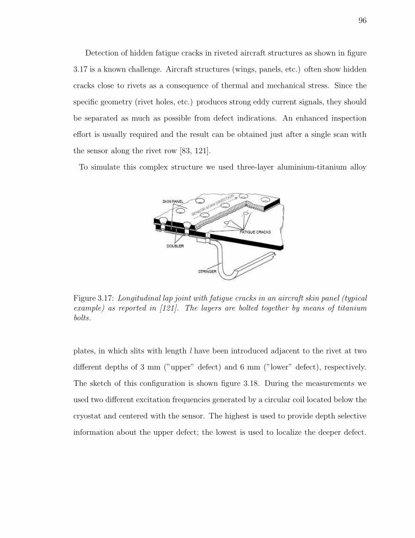
96
Detection of hidden fatigue cracks in riveted aircraft structures as shown in figure
3.17 is a known challenge. Aircraft structures (wings, panels, etc.) often show hidden
cracks close to rivets as a consequence of thermal and mechanical stress. Since the
specific geometry (rivet holes, etc.) produces strong eddy current signals, they should
be separated as much as possible from defect indications. An enhanced inspection
effort is usually required and the result can be obtained just after a single scan with
the sensor along the rivet row [83, 121].
To simulate this complex structure we used three-layer aluminium-titanium alloy
Figure 3.17: Longitudinal lap joint with fatigue cracks in an aircraft skin panel (typicalexample) as reported in [121]. The layers are bolted together by means of titaniumbolts.
plates, in which slits with length l have been introduced adjacent to the rivet at two
different depths of 3 mm (”upper” defect) and 6 mm (”lower” defect), respectively.
The sketch of this configuration is shown figure 3.18. During the measurements we
used two different excitation frequencies generated by a circular coil located below the
cryostat and centered with the sensor. The highest is used to provide depth selective
information about the upper defect; the lowest is used to localize the deeper defect.

97
Figure 3.18: Sketch of a simulated wing splice. In the three-layer aluminium titaniumalloy (AlTi) sample, the slots are positioned adjacent to the rivet in two differentdepths of 3 mm (”upper” defect) and 6 mm (”lower” defect), respectively.
When the coil scans over the plates, the in-phase and out-of-phase SQUID readout at
the excitation frequencies are recorded as a function of X-Y positions. The stand-off
distance, the spacing between SQUID and top sample, was chosen to be more than 2
mm.
The figure 3.19 shows field map distribution above the first sample configuration,
three aluminium plates with simulated fatigue crack close to the rivet in the second
layer. The excitation coil, aligned perpendicular to the z-axis, is fed sinusoidally with
an excitation frequency of 889 Hz and an amplitude of 400 mV.
We perform the phase rotation analysis for six different values of phase angles:
φ = 0o, 65o, 75o, 83o, 97o, and 125o. The bolt and crack signals are best enhanced for
a phase angle φ = 83o, due to a reduction of the lift-off effect. For this angle value,
it is evident the different current distortion around the bolt caused by the simulated
fatigue crack. However, the bolt signals are enhanced as the defect, thus having equal
phase shift. Nevertheless, the defect with a length of 4 mm and a width of 100 µm
located to a depth larger than 5 mm, has been detected applying this technique.

98
Finally, the figure 3.20 shows the magnetic field map distribution above the second
sample configuration, three aluminium plates with simulated fatigue cracks close to
the rivet in the third layer. In this case, to enhance the density of eddy currents in
the bottom plate, we decreased the excitation frequency at 421 Hz and increased the
voltage amplitude to 2 V. From the experimental results, it is absolutely clear that
the crack was well detected applying the phase angle rotation analysis, even though
we doubled the distance between the lower defect and the sensor, that in the present
case is of order of 8 mm. The enhancement of the signal obtained at φ = 53o was
broader than the signals collected in the previous case, due to the increment of the
stand-off distance and the slower variation of signals that now are close to the noise
system limit. However, it is still evident the current distortion around the bolt caused
by the simulated fatigue crack.
In conclusion, with this examples we have demonstrated how to performe eddy
current NDT with our scanning SQUID microscope. In addition, we have demon-
strated the validity of the phase rotation method used as depth-selective analysis of
cracks in structures of aeronautical interest. Superior system performance may be
obtained by increasing the dynamic range of the SQUID [98]. This requires an addi-
tional feedback coil inductively coupled to the input SQUID coil. Nulling the SQUID
signal is advantageous because the passive field minimization procedure described
above does not guarantee perfect signal cancellation. Then, the SQUID response
to the the unflawed sample can be minimized by adjusting the current fed to the
feedback coil.

99
φ = 0°
X [mm]
Y [m
m]
−5 0 5
−10
0
10
φ = 65°
X [mm]
Y [m
m]
−5 0 5
−10
0
10
φ = 75°
X [mm]
Y [m
m]
−5 0 5
−10
0
10
φ = 83°
X [mm]
Y [m
m]
−5 0 5
−10
0
10
φ = 97°
X [mm]
Y [m
m]
−5 0 5
−10
0
10
φ = 125°
X [mm]
Y [m
m]
−5 0 5
−10
0
10
Figure 3.19: The phase angles rotation analysis in the excited magnetic field appliedto a specimen, three aluminium alloy plates with a simulated fatigue crack close tothe rivet in the second plate. At φ = 0o, the component of the signal in phase withthe exciting field does not give information about the presence of buried defects; byincrementing the values of the phase angle, we observe that for φ = 83o the signal dueto the hidden defects has the largest increment since the lift-off effect is completelyeliminated. At φ = 125o the signal inverts its polarity.

100
φ = 0°
X [mm]
Y [m
m]
−5 0 5
−10
0
10
φ = 45°
X [mm]
Y [m
m]
−5 0 5
−10
0
10
φ = 50°
X [mm]
Y [m
m]
−5 0 5
−10
0
10
φ = 53°
X [mm]
Y [m
m]
−5 0 5
−10
0
10
φ = 57°
X [mm]
Y [m
m]
−5 0 5
−10
0
10
φ = 75°
X [mm]
Y [m
m]
−5 0 5
−10
0
10
Figure 3.20: The phase angle rotation analysis in the excited magnetic field appliedto a specimen, three aluminium alloy plates with a simulated fatigue crack close tothe rivet in the third plate. At φ = 0o, the component of the signal in phase withthe exciting field does not give information about the presence of hidden defects; byincreasing the values of the phase angle, we observe that for φ = 53o the signal dueto the hidden defects has the largest increase since the lift-off effect is completelyremoved. At φ = 75o the signal reverses its polarity.

Chapter 4
Scanning SQUID Microscopy: DCTechnique
NDE DC technique based on high-Tc scanning SQUID microscope with samples at
room temperature is a promising technique that we propose to apply in new fields of
interest. Using the DC technique, magnetic field distribution produced by remanent
magnetization or induced magnetization of ferromagnetic sample can be visualized.
The worst limitation of a SSM is the limited spatial resolution for the analysis of
objects at room-temperature. On the contrary, the main advantage is a direct mea-
sure of magnetic macro-domain structure and the capability to extract quite easily
information on their orientation and magnetization.
In the first section, an important aspect such as the visualization of the magnetic
moment of ferromagnetic particles, is focused on taking into account the quantitative
analysis of the data. We introduce a model for magnetic data interpretation, starting
from the analytical expression of ”point magnetic dipole”, and show the necessity
to developed a new theoretical approach, describing the magnetic sources in terms
of magnetic moment of ”extended” dipoles. Theoretical aspects are illustrated and
101

102
confirmed experimentally by measuring magnetic dipole samples.
The second section is entirely dedicated to the understanding of the detection of
magnetic dipole domains in different fields. For example, the imaging of magnetic
particles on magnetic data storage is reported as a function of an external applied
magnetic field. On the other hand, we propose to apply this non destructive tech-
nique in archeometry, it may be used to date ancient mural paintings on the base of
magnetization direction of the magnetic components.
In the last section, it has been exploited the system capability and advantages
of Scanning SQUID Microscope for the detection of crack initialization in structural
stainless steel objects. It has been implemented by monitoring the residual magne-
tization above the surface, as a consequence of mechanical stress or fatigue cycles.
Dislocation movements and magnetic filed distributions in proximity of the crack have
been well detected. The series of experimental results are really novel in this field
due to the high performances of our system.

103
4.1 Magnetic dipoles detection
in this paragraph we introduce the model for magnetic data starting from the expres-
sion of the vector potential of ”point magnetic dipole”. We emphasize the fact that
real samples are represented by a collection of magnetic dipoles and show how SSM
images can be nicely reproduced if magnetic dipoles are distributed appropriately.
The analysis serves as a reference for samples of more complex unknown structures
and to determine characteristics of magnetic material, such as magnetization.
In the first example shown in figure 4.1, two different magnetic dipole orientations
have been considered. In fig. 4.1 (a) and (b), the magnetic dipole moment of the
magnetic particle was oriented parallel to the x-axis; in the second case, fig. 4.1 (c)
and (d), the magnetic moment was oriented vertically along the z-axis.
The quantitative analysis of the scanned data can be performed on the basis of the
magnetic field distribution B [T] generated by the magnetic dipole ~m that is directly
correlated to the vector potential A by the relation B = ∇×A. The vector potential
A(~r) at position ~r(x, y, z) due to the magnetic moment ~m is
A =µ0
4π
~m × ~r
~r3(4.1.1)
where µ0 = 4π × 10−7Hm−1 is the vacuum permeability, ~m [Am2] is the magnetic
moment of the dipole, and ~r is the distance from the dipole to the measurement point.
In general, it is possible to calculate the components of the magnetic field generated

104
−10 0 10−40
−20
0
20
40
X [mm]
Am
plitu
de [µ
T]
mx
D = 4 mm D=4 mm
(a) (b)
(c) (d)
−10 0 10−2
−1
0
1
2
X [mm]A
mpl
itude
[µT
]
mx
D = 1.5 cm
−10 0 10−8
−6
−4
−2
0
2
X [mm]
Am
plitu
de [µ
T]
mz
D = 1.5 cm
−10 0 10−80
−60
−40
−20
0
20
X [mm]
Am
plitu
de [µ
T]
mz
D = 4 mm
Figure 4.1: Examples of the measurement when the magnetic moment of the particleis (a) parallel to the x-axis and (c) parallel to the z-axis. The effect of the incrementof sensor-to-sample distance for particle (b) parallel to the x-axis and (d) parallel tothe z-axis.

105
by a magnetic moment ~m at a generic point ~r (x, y, z) in the space. Since our magne-
tometer is oriented along the z-axis and it is placed in the XY-plane at height h, we
are interested to calculate the magnetic field component parallel to the z-axis, Bz(x,
y, h).
Figure 4.2: Schematic representation of the three components mx, my and mz of amagnetic moment ~m arbitrarily oriented in the space.
In figure 4.2, we consider the SQUID sensor at a distance h above a point magnetic
dipole of moment ~m, located at the origin of the cartesian coordinate system. The
magnetic moment ~m can be expressed as the sum of the three components on the axes
mx = m cos ϕ sin ϑ
my = m sin ϕ sin ϑ
mz = m cos ϑ
(4.1.2)
where ϑ is the angle between the magnetic moment ~m and the z-axis, and ϕ is the
angle of the vector projection between the y-axis and the XY plane.

106
As a matter of fact, the scan data curve shown in figure 4.1 (a), with the magnetic
moment parallel to x-axis, can be described by the following equation:
Bz,x(x, y, z) =µ0
4π3mx
xz
(x2 + y2 + z2)5/2(4.1.3)
and, if the the magnetic moment is parallel to the y-axis, the equation becomes
Bz,y(x, y, z) =µ0
4π3my
yz
(x2 + y2 + z2)5/2(4.1.4)
When the scan data curve with the magnetic dipole parallel to z-axis (fig. 4.1 (c))
can be described by the equation
Bz,z(x, y, z) =µ0
4πmz
(3z2 − (x2 + y2 + z2))
(x2 + y2 + z2)5/2(4.1.5)
Finally, for a sensor to sample distance h and a magnetic dipole arbitrarily oriented
in the space, the magnetic field measured by the SQUID sensor is equal to the sum
of the three components Bz,i, with i = x, y, z:
Bz(x, y, h) = Bz,x(x, y, h) + Bz,y(x, y, h) + Bz,z(x, y, h) (4.1.6)
By the light of this considerations, the scanning SQUID microscope system can be
applied to determine the distribution of magnetic particles in the sample. This can be
done in principle by recording the 2D magnetic dipole distribution maps followed by
a computer deconvolution of the inverse dipole problem. In figure 4.3, the magnetic

107
mz
X [mm]
Y [m
m]
−10 0 10
−10
0
10
mx
X [mm]
Y [m
m]
−10 0 10
−10
0
10
my
X [mm]
Y [m
m]
−10 0 10
−10
0
10
m45°
X [mm]
Y [m
m]
−10 0 10
−10
0
10
Figure 4.3: 2D magnetic maps simulating magnetic field distributions for differentrelative orientations of the sensor and magnetic moment ~m of the dipole: (a) ~m isparallel to z, (b) ~m is parallel to x, (c) ~m is parallel to y and (d) ~m is oriented at 45o
between the x and y axis.
108
2D maps of different relative orientations of the magnetic moment with respect to the
sensor orientation have been simulated using the eqs. 4.1.3-4.1.5: (a) ~m is parallel to
z, (b) ~m is parallel to x, (c) ~m is parallel to y and (d) ~m is oriented at 45o between
the x and y axes.
In addition, the azimuthal angle ϑ of the magnetic moment ~m may vary arbitrarily
with respect to the z-axis and the dipole will be out-of-XY plane. This other situation
is represented in figure 4.4, where 2D magnetic images of the magnetic moment ~m
oriented at ϕ = 45o between the x and y axes have been obtained varying the ϑ angle
from 90o to 0o. Six different configurations are reported: ϑ = 90o, corresponding
to the case in which ~m is placed in the XY plane and the positive and negative
peaks are symmetric; decreasing ϑ from 60o to 30o, ~m is moving out-of-XY plane
and the positive peak is more intensive than the negative peak; ϑ = 0o, where ~m
is parallel to the z-axis and finally, ϑ = −45o, in which ~m inverts its polarity. This
example shows how the magnetic source visualization can vary as a function of its
slight inclination (few degrees) with respect to the sensor plane. For this reasons, the
interpretations of experimental data could be not trivial and in some uncertain cases,
it could be necessary to use additional scans with different sensor orientations for a
unique problem solution.

109
ϑ = 90°
Y [m
m]
−10 0 10
−10
0
10
ϑ = 60°
Y [m
m]
−10 0 10
−10
0
10
ϑ = 45°
Y [m
m]
−10 0 10
−10
0
10
ϑ = 30°
Y [m
m]
−10 0 10
−10
0
10
ϑ = 0°
X [mm]
Y [m
m]
−10 0 10
−10
0
10
ϑ = −45°
X [mm]
Y [m
m]
−10 0 10
−10
0
10
Figure 4.4: 2D magnetic maps simulating magnetic field distributions for differentrelative orientations of the SQUID and magnetic moment ~m of a single dipole whenthe angle ϕ is 45o and the angle ϑ varies from 90o to 0o. (a) ϑ = 90o, ~m is placed inthe XY plane as shown by the symmetrical poles; from (b) to (d), ϑ varies from 60o
to 30o, ~m is moving out-of-XY plane as shown by the asymmetrical poles; (e) ϑ = 0o,~m is parallel to the z-axis; (f) ϑ = −45o, ~m inverts its polarity.

110
4.1.1 Imaging resolution and magnetic source sensitivity
As defined by Wikswo [120] and shown in figure 4.5, the imaging resolution is the
ability to discriminate between two closely spaced sources, such as a pair of magnetic
dipoles and a single source with the total strength equal to the sum of the single
dipoles.
Figure 4.5: Imaging resolution as reported in [120]: the ability of a magnetometerto distinguish between one single source and a pair of closely spaced sources with thesame total strength.
Using a point moment approximation, we can derive the analytical expressions
to estimate both the smallest detectable magnetic moment mmin and the imaging
resolution δ of our microscope. To this aim, we consider as a source a point magnetic
dipole ~m oriented along the z-axis (mx = my = 0), a SQUID pick-up coil radius rs
= 35 µm (congruously with our sensor) and assume that the magnetic flux through
the SQUID sensor Φc0 is of the order of√
SΦ∆f , where SΦ is the flux noise spectral
density of the system and ∆f the bandwidth of data acquisition. The estimated SSM
flux noise is S1/2Φ = 50 × 10−6Φ0/Hz1/2, so that we calculate the minimum magnetic

111
moment we can detect by the relation, as reported in [117],
mmin =2(h2 + r2
s)3/2
√SΦ∆f
µ0r2s
(4.1.7)
Choosing a sensor-to-source distance h = 200 µm and a bandwidth of 10 Hz, we
obtain the minimum detectable magnetic moment mmin = 3.5 × 10⁻¹⁵Am2.
For small displacement δ ≪ (rs, h), we find an analytical solution for the spatial
resolution δ of a circular loop SQUID sensor as a function of the geometrical param-
eters rs and h, (see [2]):
δ = (SΦ∆f)1/2
µ0mG(rs, h)1/2 (4.1.8)
where G(rs, h) is a geometrical factor. Using the previous values for rs and h, we
estimate an image resolution δ ≃ 120 µm, for the case corresponding to the minimum
detectable magnetic moment.
As a consequence, if the size of the particle is much smaller than the distance
between the particle and the SQUID sensor, the model of localized point magnetic
dipole can be applied for particle data analysis. As an example, figure 4.6 shows the
2D magnetic images generated by a point magnetic dipole oriented along the y-axis
(mx = mz = 0), simulated by using equation 4.1.4. The dipole strength is chosen as
my = 10−6Am2, providing a magnetic field value in the range 0.05 − 50 µT , at four
different h values: h1 = 1 mm, h2 = 2 mm, h3 = 5 mm and h4 = 10 mm. When h

112
h = 1 mm
X [mm]
Y [m
m]
−10 0 10
−10
0
10
h = 2 mm
X [mm]Y
[mm
]
−10 0 10
−10
0
10
h = 5 mm
X [mm]
Y [m
m]
−10 0 10
−10
0
10
h = 10 mm
X [mm]
Y [m
m]
−10 0 10
−10
0
10
(a) (b)
(c) (d)
Figure 4.6: Simulated 2D magnetic distribution maps of a point dipole positioned inthe XY plane and oriented along the y-axis. The maps are obtained for four differentsensor-to-source distances: (a) h1 = 1 mm, (b) h2 = 2 mm, (c) h3 = 5 mm, and (d)h4 = 10 mm.

113
decreases, we may observe a corresponding reduction of the axial distance between
the positive and negative poles representing the magnetic moment strength. This is
a direct consequence of dimensionless point moment model.
On the other hand, since the SSM spatial resolution is evaluated to be δ ≈ 70
µm, the point magnetic dipole approximation becomes an unrealistic attainable limit,
except for very large h values or very small magnetic sources. Indeed, the comparison
between experimental and simulated magnetic dipole shown in figure 4.7 demonstrate
that a different approach is needed to reproduce the magnetic field distribution of real
extended magnetic sources with dimensions larger than the SSM spatial resolution.
As shown in this case, where the source is a ferromagnetic rod specimen 10 mm long,
if the sensor-to-source distance is longer than the source dimension (h = 16 mm), the
point magnetic model fits pretty good the results (compare (b) and (d) in figure 4.7),
while if the source dimension is comparable or less than the sensor-to-source distance
(h = 5 mm), the point magnetic dipole does not work well (compare (a) and (c) in
figure 4.7).
Consequently, in the next section we derive a simple theoretical approach which
allows the description and simulation of extended magnetic dipoles to be applied in
the case of 1D ferromagnetic particle of finite dimensions.
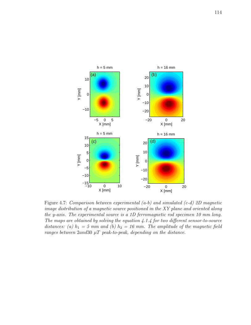
114
h = 5 mm
X [mm]
Y [m
m]
−5 0 5
−10
0
10
h = 16 mm
X [mm]
Y [m
m]
−20 0 20
−20
−10
0
10
20
h = 5 mm
X [mm]
Y [m
m]
−10 0 10−15
−10
−5
0
5
10
15h = 16 mm
X [mm]
Y [m
m]
−20 0 20
−20
−10
0
10
20
(a) (b)
(c) (d)
Figure 4.7: Comparison between experimental (a-b) and simulated (c-d) 2D magneticimage distribution of a magnetic source positioned in the XY plane and oriented alongthe y-axis. The experimental source is a 1D ferromagnetic rod specimen 10 mm long.The maps are obtained by solving the equation 4.1.4 for two different sensor-to-sourcedistances: (a) h1 = 5 mm and (b) h2 = 16 mm. The amplitude of the magnetic fieldranges between 2and30 µT peak-to-peak, depending on the distance.

115
4.1.2 Extended magnetic dipole approximation
As said before, if the magnetic source dimension is comparable with the image reso-
lution δ of our system, its signal cannot be simulated in the framework of the point
magnetic moment approximation. For this reason, it is useful to introduce a finite
length magnetic dipole approximation, that we call the multi-dipole (MD) model.
The idea is to consider an extended dipole as made of N aligned point magnetic
dipoles spaced ∆c ≈ δ, which constitutes a single 1D macro-domain. The magnetic
field of an extended dipole of length L will be the sum of the magnetic fields of N
single point magnetic dipoles of length L = N∆c. More details about the develop-
ment of this model and different kinds of magnetic dipole configurations are treated
by Adamo et al. in [2].
Thus, the magnetic field components Bz,i generated by an extend magnetic dipole
can be still expressed as a function of the magnetic moment components mx, my and
mz, as reported in [2] and summarized in the following equations:
Bz,x =µ0
4π3mxz
N∑
i=1
(x − ∆cix)
[(x − ∆cix)2 + (y − ∆ciy)2 + (z − ∆ciz)2]5/2(4.1.9)
Bz,y =µ0
4π3myz
N∑
i=1
(y − ∆ciy)
[(x − ∆cix)2 + (y − ∆ciy)2 + (z − ∆ciz)2]5/2(4.1.10)

116
Bz,z =µ0
4πmz
N∑
i=1
3z2 − [(x − ∆cix)2 + (y − ∆ciy)
2 + (z − ∆ciz)2]
[(x − ∆cix)2 + (y − ∆ciy)2 + (z − ∆ciz)2]5/2(4.1.11)
where ∆cix, ∆ciy and ∆ciz are the projections of the point magnetic dipole displace-
ment ∆c on x, y and z-axis, respectively.
The first important consequence obtained introducing the MD model, is that it
is possible to fit the data for a magnetic dipole with finite dimensions comparable
or larger than the spatial resolution of the system. As an example in figure 4.8, we
consider again the case of 1D magnetic dipole source of length L = 10 mm, laying
in the XY plane and parallel to the y-axis (see figure 4.8 (a) and (b)). Using the eq
4.1.10 and choosing N = 110 point magnetic dipoles with strength my = 10−6Am2
spaced of ∆c = 100 µm, we computed the responses at two different distances, h1 =
5 mm and h2 = 16 mm (see figure 4.8 (c) and (d), respectively). As shown in this
example, using the MD model, there is an excellent quantitative agreement between
experimental and simulated data, either in the case in which the sensor-to-source
distance is larger than the dimension of the magnetic particle (figure 4.8 (b) and (d)),
or when tit is less than the magnetic particle dimension (figure 4.8 (a) and (c)).
Moreover, in the next section, we want to stress the attention to the fact that
the MD model is valid either when the dimension of single dipole is smaller than
the system image resolution δ, or in the opposite limit, when the sensor-to-sample
distance h is comparable or less than the dimension of a single magnetic particle.
This concept will be more clear when we apply the MD model to a magnetic sources

117
h = 5 mm
X [mm]
Y [m
m]
−10 0 10−15
−10
−5
0
5
10
15h = 16 mm
X [mm]
Y [m
m]
−20 0 20
−20
−10
0
10
20
h = 5mm
X [mm]
Y [m
m]
−10 0 1010
−10
0
10
h = 16mm
X [mm]
Y [m
m]
−20 0 20
−20
−10
0
10
20(a) (b)
(c) (d)
Figure 4.8: Comparison between experimental (a-b) and simulated (c-d) 2D magneticsource distribution using the MD model. A magnetic source 10 mm long is positionedin the XY plane and oriented along the y-axis. The parameters used for the simula-tions are: N = 110 point magnetic dipoles, each with strength my = 10−6Am2, spacedby ∆c = 100 µm. The responses are computed at two different distances, h1 = 5 mmand h2 = 16 mm. The amplitude of the magnetic field ranges between 2 and 30 µTpeak-to-peak, depending on the distance.

118
composed of multiple dipoles randomly oriented in the space.
4.1.3 Extended model for two magnetic sources
We describe the MD model for the detection of two different magnetic particles posi-
tioned in the XY plane. In particular, the two experimental particles are both 4 mm
long: the magnetic source ~m1 is oriented along the y-axis and ~m2 forms an angle of
45o between the x and y-axis, as shown in the sketch of figure 4.9.
We performed two kinds of measurement. In the first case, the magnetic field
distribution Bz, above the two magnetic sources ~m1 and ~m2, is obtained at the height
h = 1.5 mm, smaller than the length of the single 1D magnetic particle. The two
sources, both 4 mm long, are well detected and their magnetic field distributions do
not affect considerably each other, as shown in figure 4.9 (a). In the second case, the
magnetic field distribution Bz is obtained at the height h = 5 mm, larger than the
single dipole length, thus the magnetic signatures overlap and the imaging resolution
gets worse. As it is evident, this time we cannot distinguish the two different mag-
netic sources (figure 4.9 (b)). We have also made measurements for the same different
heights when the polarity of ~m2 source is inverted, as shown in figure 4.9 (c) and (d),
for h = 1.5 mm and h = 5 mm, respectively.
Using the MD model and choosing as fitting parameters N = 10 point magnetic
dipoles spaced by ∆c = 400 µm, we computed the responses at two different dis-
tances, h1 = 1.5 mm and h2 = 5 mm obtaining a magnetic dipole strength for both

119
h = 1.5 mm
X [mm]
Y [m
m]
−5 0 5
−5
0
5
h = 5 mm
X [mm]
Y [m
m]
−10 0 10
−10
−5
0
5
10
h = 1.5 mm
X [mm]
Y [m
m]
−5 0 5
−5
0
5
h = 5 mm
X [mm]
Y [m
m]
−10 0 10
−10
−5
0
5
10
Sourcedistributionm
1m
2
Sourcedistributionm
2m1
+
+− −
−−
+
+
+
+−
−
− −
+
+
(a)
(b)
(c)
(d)
Figure 4.9: Experimental 2D magnetic maps of two magnetic rods 4 mm long, posi-tioned in the XY plane. The dipole ~m1 is oriented along the y-axis, while the dipole~m2 forms an angle of 45o between the x and y-axis. Two different configurations aremeasured, obtained by 180o in-plane rotation of ~m2 at two different sensor-to-sourcedistances: h1 = 1.5 mm and h2 = 5 mm. The amplitude of the magnetic field rangesbetween 5 - 60 µT peak-to-peak, depending on the distance.

120
sources of order of m ≃ 10−6Am2. This value can be used to calculate the mag-
netization M [A-turn m−1] of the sample, that is defined as the magnetic moment
per unit volume: M = Nm/V . The estimate magnetization for the ferromagnetic
rod particle specimens, of radius 400 µm and 4 mm long, is about M ≃ 5 kAturn m−1.
However, it is worth nothing that, even in the case of a single dipole, the inter-
pretation of magnetic maps may need additional information. Using the MD model,
the inverse problem for the magnetic moment could be solved, but additional scans
with other sensor orientations are necessary for a unique solution of the problem.

121
4.2 Imaging magnetic domain structures
Since real samples under investigation often show a collection of extended magnetic
dipoles with different orientations, we present in this section the measurements per-
formed by SSM over different magnetic samples. Because of its extremely large sen-
sitivity (few tens of pT/Hz1/2), combined with a good spatial resolution (few tens of
µm), the SSM is able to detect information contained in thin magnetic films or other
type of magnetic objects.
Quite recently, magnetic recording media (computer storage, credit cards, etc.) is
a large and growing field of use of magnetic materials. The trend is to require high-
density magnetic recording systems. We report a two-dimensional magnetic image
produced above a magnetic material surface that can be used to estimate the spatial
variation of magnetization, which is of interest in magnetic recording materials [49].
In a totally different field, there is a particular interest in the archeometry dating,
which widely used to acquire information of the physical data of an ancient find,
comparing the ”frozen” direction of magnetization within an archaeological feature
with a time reference curve. Here we propose to apply this non-destructive technique,
completely innovative in the archeological field, to find information on magnetization
direction and, at the same time, as a form of authentication of artistic patrimony.

122
4.2.1 Imaging magnetic recording media
This experiment was performed to test the feasibility to use a scanning SQUID mi-
croscope from reading information from magnetic recording media, in this case a
commercial floppy disk, and to estimate the value of magnetic signals.
The floppy disk presents a thin layer of Fe-Co based microparticles with size of
about 1 µm. These magnetic particles have in-plane oriented magnetic moments.
The coercivity value, the intensity of the applied magnetic field required to reduce
the magnetization of such ferromagnetic materials to zero, is of about 30-70 kA m−1.
Such magnetic moments are initially in-plane randomly oriented. During the format-
ting process, the magnetic tracks are created and each magnetic moment orientation
is equivalent to a ”zero” state of data. During recording process, some magnetic mo-
ments are magnetized in the opposite direction, thus some magnetic pole orientations
are equivalent to ”unit”.
The sample we measured was a fragment of a floppy disk with some recording data
corresponded to text information. Figure 4.10 (above) shows the magnetic image of
the fragment portion taken at the sensor-to-sample distance of about 100 µm. The
intensity of the magnetic field distribution varies from about -3 µT (blue peaks) to +3
µT (red peaks). The minimum size of a single spot is about 200 µm, corresponding
to the used step resolution. Thus, our imaging resolution makes impossible to resolve
the single magnetic domain of recording media (one bit of information of order of few
microns).

123
Recorded data
X [mm]
Y [m
m]
−5 0 5
−5
0
5
Recorded data after magnetization
X [mm]
Y [m
m]
−5 0 5
−5
0
5
−50
5
−50
5
−6−4−2
0
X [mm]
Recorded data
Y [mm]
B [µ
T]
−50
5
−50
5
−20246
X [mm]
Recorded data after magnetization
Y [mm]
B [µ
T]
Figure 4.10: Magnetic images of recorded data on a commercial floppy disk (above)and the effect of the distortion of some recorded data after magnetization of the sample(below). The amplitude of the magnetic field ranges between -3 to 3 µT peak-to-peak.

124
Figure 4.10 (below) shows the magnetic image of the fragment portion taken at
sensor-to-sample distance of about 100 µm when the sample was previously magne-
tized with a static magnetic field. The intensity of the magnetic field distribution
still varies in the range of ± 3 µT , but the less intensive magnetic domains are de-
stroyed. However, the effect of the pre-magnetization is that the periodic structure
of the recorded information is modified with the consequent loss of data.
4.2.2 Imaging magnetic particles in ancient mural painting
In this section we give a quick look to the analysis of archaeological ruins. For sake
of completeness, the archaeological activity based on magnetic techniques can be di-
vided into two main categories:
Magnetic survey. It is based on geophysical prospecting which deals with iron min-
erals within the soils and sediments forming archaeological sites, that often provide a
valuable record of past human activity. This technique represents an important aid
for the location and interpretation of archaeological ruins. This aspect is obviously
not of interest for the magnetic microscopy and so we do not treat it in this contest.
Archaeomagnetic dating. It is based on the measurement of magnetic properties
from samples recovered during excavation. Naturally occurring processes of magneti-
zation can result in the alignment of individual magnetic grains along the orientation
of the earth magnetic field. Since this field has constantly changed direction during
geological time scales, the determination of a ”frozen” direction of magnetization can
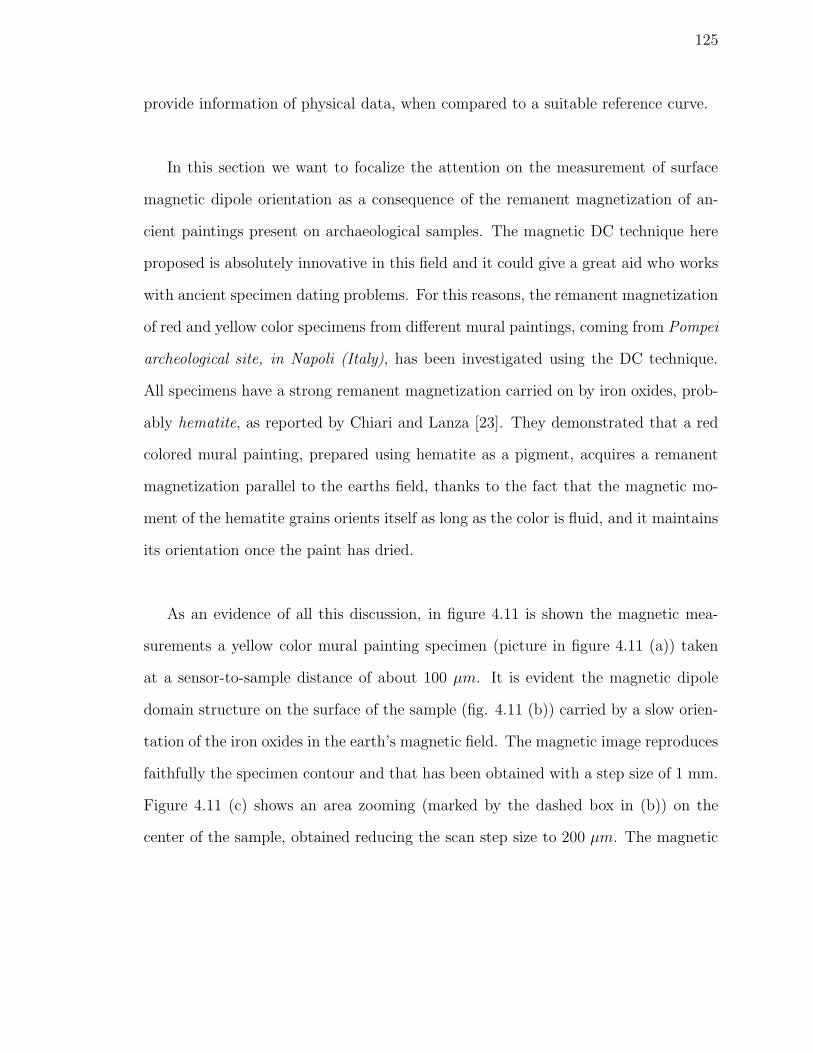
125
provide information of physical data, when compared to a suitable reference curve.
In this section we want to focalize the attention on the measurement of surface
magnetic dipole orientation as a consequence of the remanent magnetization of an-
cient paintings present on archaeological samples. The magnetic DC technique here
proposed is absolutely innovative in this field and it could give a great aid who works
with ancient specimen dating problems. For this reasons, the remanent magnetization
of red and yellow color specimens from different mural paintings, coming from Pompei
archeological site, in Napoli (Italy), has been investigated using the DC technique.
All specimens have a strong remanent magnetization carried on by iron oxides, prob-
ably hematite, as reported by Chiari and Lanza [23]. They demonstrated that a red
colored mural painting, prepared using hematite as a pigment, acquires a remanent
magnetization parallel to the earths field, thanks to the fact that the magnetic mo-
ment of the hematite grains orients itself as long as the color is fluid, and it maintains
its orientation once the paint has dried.
As an evidence of all this discussion, in figure 4.11 is shown the magnetic mea-
surements a yellow color mural painting specimen (picture in figure 4.11 (a)) taken
at a sensor-to-sample distance of about 100 µm. It is evident the magnetic dipole
domain structure on the surface of the sample (fig. 4.11 (b)) carried by a slow orien-
tation of the iron oxides in the earth’s magnetic field. The magnetic image reproduces
faithfully the specimen contour and that has been obtained with a step size of 1 mm.
Figure 4.11 (c) shows an area zooming (marked by the dashed box in (b)) on the
center of the sample, obtained reducing the scan step size to 200 µm. The magnetic

126
Yellow mural painting specimen
X [mm]
Y [m
m]
−20 −10 0 10 20−20
−10
0
10
20
X [mm]
Y [m
m]
−4 −2 0 2 4−4
−2
0
2
4
−4 −2 0 2 4−3
−2
−1
0
1
X [mm]
B [µ
T]
1 cm
(a)(b)
(c)
(d)
Figure 4.11: Magnetic images of a yellow color mural painting specimen coming fromPompei archeological site (Italy) taken at a sensor-to-sample distance of about 100µm. (a) picture of the specimen; (b) magnetic image of the sample with the evidentsurface magnetic dipole distribution as a consequence of iron oxides orientation inearth’s magnetic field; (c) magnetic image zooming on the center of the sample, asmarked by the dashed box in (b), using 200 µm scan step size; (d) two line scans ofthe magnetic field, as marked by the dashed lines in (c).

127
field varies in the range of ± 2 µT peak-to-peak, as reported in figure 4.11 (d), where
two line scans along the dashed lines in figure 4.11 (c) are reported.
The second red color mural painting specimen, shown in figure 4.12 (a), has similar
characteristics. The magnetic image, taken at a sensor-to-sample distance of about
100 µm, still shows the magnetic dipole domain distribution on the surface of the
sample (figure 4.12 (b)), as a consequence of the slow orientation of the iron oxides in
the earth’s magnetic field. The zooming images (figure 4.12 (c)) on a central area of
the sample (marked by the dashed box in (b)) is obtained using 400 µm scan step size.
The magnetic field variation is once again of ± 2 µT peak-to-peak as shown in fig-
ure 4.12 (d), where two line scans along the dashed lines in figure 4.12 (c) are reported.
Due to the quite recent development of the used DC technique, it is the first time
that this kind of magnetic domain distribution is observed on ancient mural paintings
whit ferromagnetic properties. Something similar has been made when some authors
visualized magnetic images of rocks of geological interest.
In the following, we want to focus on another important aspect. Some colors, espe-
cially reds and yellows, used today for the conservation of artistic painting patrimony,
are characterized by ferromagnetic properties due to iron oxide pigments. However,
the patterns shown in figures 4.11 and 4.12 are typical of ancient finds and, in the
future, they can probably be used for the identification of the authenticity of the
ancient paintings and maybe to date a specific piece of art. From this point of view,
non destructive forms of authentication is of great importance since it contributes to
the preservation and conservation of artistic patrimony and even to prevent forgery.
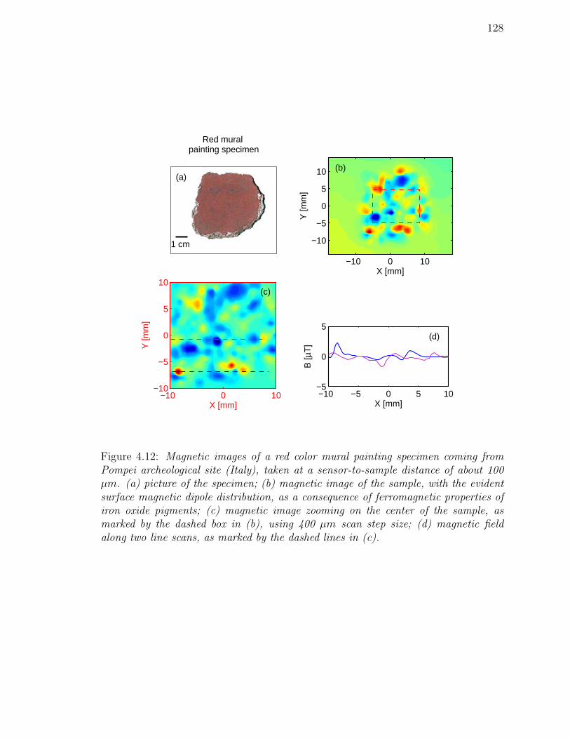
128
Red mural painting specimen
(b)
X [mm]
Y [m
m]
−10 0 10
−10
−5
0
5
10
X [mm]
Y [m
m]
−10 0 10−10
−5
0
5
10
−10 −5 0 5 10−5
0
5
X [mm]
B [µ
T]
1 cm
(b)(a)
(c)
(d)
Figure 4.12: Magnetic images of a red color mural painting specimen coming fromPompei archeological site (Italy), taken at a sensor-to-sample distance of about 100µm. (a) picture of the specimen; (b) magnetic image of the sample, with the evidentsurface magnetic dipole distribution, as a consequence of ferromagnetic properties ofiron oxide pigments; (c) magnetic image zooming on the center of the sample, asmarked by the dashed box in (b), using 400 µm scan step size; (d) magnetic fieldalong two line scans, as marked by the dashed lines in (c).

129
4.3 Magnetic detection of mechanical degradation
of steel
It is a considerable problem to estimate non destructively the degradation of me-
chanical property of metallic alloys, as a consequence of local plastic deformation due
to fatigue cycles, especially crack formation as a precursor of failure. This kind of
investigation may be used to examine ferromagnetic materials such as the steels used
in nuclear pressure vessels, ship hulls and other critical structures to insure safety, as
well as for on-line quality control in the manufacture of structures.
It is well known that plastic deformation of metals increases the density of dis-
locations within them. The increase in dislocation density hardens the material and
the phenomenon is known as strain-hardening. The dislocation substructure evolves
slowly and becomes increasingly heterogeneous, leading to the formation of the persis-
tent slip band (Luders bands) that will eventually nucleate cracks. They also interact
with magnetic domain walls and, therefore, change the magnetization of the steel.
The last stage of fatigue cycle is characterizes by the formation of the fatigue cracks
and ends with final failure. Since fatigue cracks can propagate under loads that are
small compared to those required to nucleate them, the time interval for crack detec-
tion between nucleation and catastrophic failure may be very short.
Therefore, since significant microstructural changes occur during the fatigue stages,
researchers have had some success in developing NDE methods probing them. Mag-
netic methods are particularly promising for ferromagnetic materials such as struc-
tural steels. Parameters such as the saturation magnetization, coercivity, Barkhausen

130
noise and magnetic hysteresis change significantly during the initial and final stages of
fatigue [90, 93]. Magneto-mechanical effect has been detected using a SQUID magne-
tometer, measuring changes in the magnetic hysteresis of metallic alloys and structural
steel. Indeed, a magnetic field sensor with high field sensitivity and spatial resolu-
tion as the SSM is required to measure the low magnetic field signals characterizing
dislocation motion. These properties are successfully satisfied by the SQUID micro-
scope that has already been used in the detection of fatigue damage [118, 109, 87, 17].
In this section, the change of the pattern by a tensile deformation has been investi-
gated in two different structural steel samples (Fe360), without applying any external
magnetic field. The specimen configurations are shown in figure 4.13. In particular,
the two different geometries are used to detect different effects: sample (1) is used to
study the initiation and crack propagation on slot tip and sample (2) to detect the
surface slip bands as a consequence of plastic deformation.
In the first subsection, a local tensile stress concentration on slot tip is visualized
Figure 4.13: Geometry of 5 mm thick structural steel (Fe360) specimens. Sample (1),with a slot 100 µm wide, is used to study the initiation and crack propagation onslot tip; sample (2) to detect the surface slip bands. A mono-axial tensile stress wasapplied along the x-direction and measured by the strain-gauges glued on both side ofthe samples. The dashed boxes indicate the inspected regions.

131
before and after tensile stress cycles. The mechanical effect is correlated to the mag-
netic field gradient component dBz/dx. The capability of the SSM to detect magnetic
signals, produced by plastic deformation, has been demonstrated.
In the second subsection, Luders bands, which are groups of slip bands, appearing
on the plate surface after one tensile stress cycle, were observed at the corresponding
locations of the stripes. This shows that fine deformation can nondestructively be
detected using SSM.
4.3.1 Detection of fatigue crack in steel due to fatigue cycles
In the first example, ten mono-axial tensile stress cycles, along the x-direction and
ranging from 0 to 32 kN, was applied to a pre-demagnetized rectangular specimen
with 100 µm width slot, shown in figure 4.13 (1). This specimen configuration has
been used to study the initiation and propagation of a crack raised on the slot tip.
A magnetic hysteresis loop due to the tensile stress cycles was measured using
Hall probe field sensor above the sample in two different positions, in proximity of
the slot tip and 20 mm far away from it. The hysteresis strength at slot tip position
was ten times greater than the value measured 20 mm away from the slot tip. as
expected, this effect is correlated to the increased number of dislocations around the
slot tip and the decreased density moving far away from it. More information on this
analysis is reported in [17].

132
To detect the plastic deformation produced by the tensile stress, magnetic mea-
surements of specimen 1 have been carried out on the tip slot area before and after
stress cycles. The magnetic images are obtained with a scan step size of 200 µm and
a sensor-to-sample distance of 5 mm. Results are shown in figure 4.14, where 2D
X [mm]
Y [m
m]
slot:before plasticization B
z
Y [m
m]
−4 −2 0 2
−5
0
5
Y [mm]
slot:after plasticization B
z
−2 0 2−2.5
−1.5
−0.5
0.5
1.5
2.52.52.5(a) (b)
Figure 4.14: 2D magnetic maps of magnetic field component Bz measured on slot tip(as marked by the dashed box in fig. 4.13 (1)) before the tensile stress (a) and afterthe mechanical load (b).
magnetic maps reporting the normal component of the magnetic field Bz measured
before any tensile stress cycle (a) is compared with the magnetic field component
Bz measured after applying tensile stress cycles (b). It could be noted that there
is a remanent magnetization concentrated around the slot border, represented by
the positive and negative area (red and blue area, respectively). This magnetization
distribution is evident also after the demagnetization process (fig. 4.14 (a)). The

133
magnetic field varies in the range of ± 15µT before applying the tensile stress and ±
20µT after the mechanical load.
In addition, we can observe that the effect of mechanical stress on the slot tip can
be enhanced if we report the magnetic field gradient dBz/dx, as shown in figure 4.15,
where a comparison between the direct signal Bz acquired by the SQUID sensor and
the gradient of signal dBz/dx across the slot tip has been reported. In particular, in
figure 4.15 (a), the 2D magnetic map of the direct signal Bz measured by the sensor
and corresponding to the slot tip has been reported. This signal can be compared
with the magnetic field gradient dBz/dx (figure 4.15 (b)), where it is more evident a
well-defined circular area around the tip, that represents the plastic deformation. In
figure 4.15 (c), a zoom area close to the tip, marked by the dashed box in figure 4.15
(a), is shown. This signal can be again compared with the magnetic field gradient
dBz/dx (figure 4.15 (d)), where it is more clear the magnetic deformed area, which
represents the crack initialization.
Based on our experience, the magnetic DC technique using SQUID microscope
could allow to detect the dynamic evolution of magnetic dislocation arising from
different mechanical tensile stress cycles until crack initialization and the consequent
specimen failure.

134
X [mm]
Y [m
m]
slot:direct signal B
z
−2 0 2
−2
−1
0
1
2
X [mm]
Y [m
m]
slot:derived signal dB
z/dx
−2 0 2
−2
−1
0
1
2
X [mm]
Y [m
m]
slot:direct signal B
z
−5 0 5−4
−2
0
2
4
X [mm]
Y [m
m]
slot:derived signal dB
z/dx
−5 0 5−4
−2
0
2
4
(a) (b)
(c) (d)
Figure 4.15: 2D magnetic map comparison between the direct signal Bz acquired bythe SQUID sensor and the signal gradient dBz/dx across the slot tip. (a) direct signalBz measured by the sensor in the correspondence of the slot tip and (b) magnetic fieldgradient dBz/dx of the same area; (c) is the direct signal of the zoomed area, markedby dashed box in (a), and (d) is the the gradient signal on the same zoomed area.

135
4.3.2 Imaging dislocations in steel due to tensile deformation
In the second example, only one mono-axial tensile stress cycle, along the x-axis and
ranging from 0 to 40 kN, was applied to a pre-demagnetized dog-bone shaped spec-
imen, shown in figure 4.13 (2). This specimen configuration gives the possibility to
investigate the effect of plastic deformation detecting the surface slip bands.
A magnetic hysteresis loop due to the tensile stress cycle was measured using
Hall probe field sensors. This means that the residual magnetization of the sample
is affected by the applied tensile stress in a reversible way. However, to detect the
magnetic field variation induced by the interaction between the dislocation motion
and the magnetization, magnetic measurement of specimen 2 has been carried out on
a scanning area with visible slip bands, as marked by the dashed box in figure 4.16
(a).
In figure 4.16 (b), the 2D magnetic map of the direct signal Bz measured by the
sensor and corresponding to some slip bands has been reported. The magnetic image
is obtained with a scan step size of 100 µm and a sensor-to-sample distance of 5 mm.
As we can observe, the dislocation signal was not easily distinguishable by the overall
residual magnetization of the sample. For this reason, we reported the magnetic field
gradient dBz/dx, in figure 4.16 (c), where the two slip bands are more evident. Typi-
cally, these slip bands precede the fatigue crack initialization after plastic deformation.
The SQUID microscope inspection, thanks to its high sensitivity to low magnetic
field and good spatial resolution, allowed us to detect and localize the band position.

136
dislocations:optical image
X [mm]
Y [m
m]
direct signal Bz
−4 −2 0 2 4−4
−2
0
2
4
X [mm]
Y [m
m]
derived signal dBz/dx
−4 −2 0 2 4−4
−2
0
2
4
−5 0 5−1
−0.5
0
0.5
X [mm]
dBz/d
x [µ
T/m
m]
line scan signal extracted from the map
1 mm
(a) (b)
(c) (d)
Figure 4.16: Magnetic field measurements induced by the interaction between the dis-location motion and the magnetization sample. (a) Visible slip band optical image;(b) the 2D magnetic map of the direct signal Bz measured on the slip bands (markedby dashed box in (a)); (c) magnetic field gradient dBz/dx on the same area; (d) linescan trough two slip bands as marked by the dashed lines in (c).

137
Since it is evident that the slip bands are already visible on the sample surface, the
magnetic field gradient yielded useful information on the presence of slip bands. The
increment of this density is a consolidated precursor of strain-hardening phenomenon
and thus its detection represents a very important information concerning material
properties before the fracture is reached. Moreover, by means of SQUID microscope
detection, it is possible to obtain information about magnetization strength due to
the single slip band. In this way, it is possible to study where the mechanical stress
produces locally changes of the sample magnetization. An example of that is pre-
sented in figure 4.16 (d), where a single line scan, extracted by the magnetic field map
as marked by the dashed lines in figure 4.16 (c), has been reported. The line plot
represents the normal component of the magnetic field gradient across two slip bands.

Conclusions
In this research activity a Non Destructive Analysis (NDA) for the investigation
of surface and sub-surface material properties based on a high-resolution Scanning
Magnetic Microscope for room-temperature objects has been presented.
The magnetic sensor used in this activity is a Superconducting QUantum Inter-
ference Device (SQUID), which is the most sensitive detector of magnetic flux that
is currently available. The present work used a semi-commercial Scanning Magnetic
Microscope prototype (SMM-770 model, by Tristan Technologies), equipped with
liquid-nitrogen cooled SQUID sensor, which has been purchased in the framework of
the regional project ”Centro di Competenza Regionale per la valorizzazione e fruizione
dei Beni Culturali e Ambientali” (CRdC-INNOVA).
The first part of this work has been dedicated to the set-up of the SSM prototype
and to its implementation. An accurate analysis in terms of spectral density noise of
the sensor and external sources of noise has been performed. The first evident source
of noise has been identified in the moving mechanism used to scan the sample under
the sensor. Indeed, during the measurement, the movement of the stepper motors
increases the environmental spectral density noise detected by the sensor of about 10
times at 100 Hz. For this reason, we have proposed to the manufacturing industry a
138

modification of the system software control, assuring that the motors are turned off
when the sensor is fixed in a measurement position. Although we used such caution,
a DC signal carried by a remanent magnetization of the metallic parts, which form
the rotational mechanisms, in principle cannot be reduced. However, we obtained
an enhancement of the signals by subtracting the sample-signal and the background
signal (that is a measurement obtained without the sample). In this way, we achieved
a further reduction of the intrinsic noise of the system and the best value we measured
for the smallest measurable magnetic field variation is of order of 0.2 -0.3 nT.
The efforts in this direction and the optimization of such aspects, as consequence
of a strictly collaboration with the Tristan Technologies, have actually made our SSM
as a reference system for their international customers. In this way, a frequent ex-
change of mutual knowledge is going on.
The second part of this work is completely dedicated to the analysis of samples
at room-temperature by means of SSM. The sensitivity of the SQUID sensor at low
frequencies allows to work as eddy-current sensor with high depth resolution. This
was used to detect flaw on paramagnetic materials. The development of SSM in
the field of eddy current non-destructive evaluation (NDE), is possible by the good
combination of sensitivity of about 20 pT/√
Hz and spatial resolution of order of 70
µm of sensor, which are actually the best values compared with the other common
sensors (flux gate, Hall probe, GMR, etc.) used for such applications.
Non destructive testing are used to determine the integrity of the structures and
flaw detection, as requirement of quality controls. This technique is widely applied
to search for flaws in joined metallic structures for aeronautical applications (part
139

of fuselage or wings). The detection of hidden defects has been widely carried out,
focusing the attention on the enhancement of the signal flaw response with respect
to the rivet signal on the surface. Indeed, hidden flaws, 100 µm wide, located under
two aluminium-titanium alloy plates has been well detected at distance more than 10
mm under the surface. To obtain these results, we have applied the method of phase
rotation analysis, which is an innovative way to enhance the signatures of the signal
under the surface respect to the signal on the surface. This method is based on the
principle of penetration depth of the eddy current analysis. Indeed, an important
property of a defect signal is the variation of its own phase, as a function of its depth
under the surface. The results obtained in this work applying such method are really
competitive in this field.
We have also developed a theoretical model describing eddy current distributions,
generated by a circular flaw, in a ”thin” conducting plate. In this assumption, we
can neglected the magnetic field variation along the thickness of the sample. Al-
though this hypothesis introduces a simplification of the problem, the solution of the
diffusion equation, used to describe electromagnetic problems in the intermediate fre-
quency range, become quickly complex in the presence of flaws. However, the novel
analytical solution we found is in good agreement with the experimental one and has
been used to analyze the response of the SQUID sensor in presence of flaws.
The last section is focused on the investigation of novel methods and new prospects
of SSM employment. We have exploited the SQUID capabilities that make it suitable
to image magnetic domain structures in ferromagnetic objects. Since the spatial
resolution of the system allows to visualize magnetic domains of order of 70 µm, a
140
theoretical approach, which describes the magnetic source as magnetic moments of
”extended” dipoles, has been developed. The model shows a great agreement with the
experimental data and it has helped us to obtain a good interpretation and a better
perspective of our results. Two innovative fields of application have been proposed.
One of this provides a direct imaging of the magnetic particle dipoles on samples
with ferromagnetic components (for example, on magnetic data storage or ancient
mural paintings). These information may be useful to estimate quite simply the
sample magnetization, and in same cases, to follow the variation of the magnetic
dipole orientations when they are subject to an external applied magnetic field. For
example, one could use this effect to provide dating of ancient work arts.
The second application concerns the requirement to estimate non destructively the
degradation of structural metallic alloys, as a consequence of local plastic deformation
due to fatigue cycles, especially crack formation as a precursor of failure. Due to the
capability of SQUID sensor to work in relatively high external magnetic field, the
significant microstructural changes (dislocation movement), which occur during the
fatigue stages, can be detected with high spatial resolution. The results are novelty in
this field. At present time, in a stress-strain mechanical test, the sample is subject to
a different numbers of fatigue cycles until it reaches the rupture. This method may be
used to follow the different stages of fatigue cycle and search for crack initialization
as failure precursor. This point is useful in applications in which safety or on-line
quality control in critical structures, such as nuclear pressure vessel, ship hulls, etc,
is required.
In the next future, we will focus our research on eddy current non destructive
141

analysis applied to innovative aeronautical structures, such as composite materials.
In the same way, also the injection current technique has shown high resolution and
field sensitivity to search for fault currents. Several electronic devices have successfully
been tested. For this reason we think that also electronic industry may derive benefits
from this SSM application.
In summary, the SSM prototype has been carefully tested and optimized in terms
of spatial resolution and field sensitivity. Both theoretical and experimental progress
for NDA on materials of aeronautical interests has been done. Novel applications,
such as NDA for electronic industry or cultural heritage, have been successfully inves-
tigated. We believe that the SSM may give further benefits also in other unexplored
research fields.
142

Bibliography
[1] D. Drung (a). Advenced SQUID read-out electronics. in: H. Weinstock and
R. W. Ralston (Ed.), SQUID Sensors: Fundamentals, Fabrication and Appli-
cations, NATO ASI serie E, vol. 329, Kluwer, Dordrecht, pages 63–116, 1996.
[2] M. Adamo (a), C. Nappi, and E. Sarnelli. Magnetic dipole imaging by a scan-
ning magnetic microscope. Meas. Sci. Technol., 19:1–10, 2008.
[3] K. Allweins, G. Gierelt, H.-J. Krause, and M.v. Kreutzbruck. Defect dtection
in thick aircraft samples based on HTS SQUID Magnetometry and pattern
recognition. IEEE Trans. Appl. Supercond., 13:250–253, 2003.
[4] P. W. Anderson and J. M. Rowell. Probable observation of the Josephson
superconducting tunneling effect. Phys. Rev. Lett., 10:230–232, 1963.
[5] D. Drung (b). High-Tc and low-Tc dc SQUID electronics. Supercond. Sci.
Technol., 16:1320–1336, 2003.
[6] M. Adamo (b), C. Nappi, and E. Sarnelli. Eddy current solution for circular
flaws in conducting thin plate. Unpublished.
[7] J. Bardeen, L. N. Cooper, and J. R. Schrieffer. Microscopic theory of supercon-
ductivity. Letters to the Editor, 1957.
[8] A. Barone and G. Paterno. Physics and applications of the Josephson effect.
John Wiley and Sons, New York, 1982.
143

144
[9] F. Baudenbacher, L. E. Fong, J. R. Holzer, and M. Radparvar. Monolithic
low-transition-temperature superconducting magnetometers for high resolution
imaging magnetic fields of room temperature samples. Appl. Phys. Lett.,
82(20):3487–3489, 2003.
[10] F. Baudenbacher, N. T. Peters, P. Baudenbacher, and J. P. Wikswo Jr. High
resolution imaging of biomagnetic fileds generated by action currents in cardiac
tissue using LTS-SQUID microscope. Physica C, 368:24–31, 2002.
[11] F. Baudenbacher, N. T. Peters, and J. P. Wikswo Jr. High resolution low-
temperature superconductivity superconducting quantum interference device
microscope for imaging magnetic fields of samples at room temperatures. Rev.
Sci. Instrum., 73(3):1247–1254, 2002.
[12] J. G. Bednorz and K. A. Muller. Possible high-Tc superconductivity in the
Ba-La-Cu-O system. Z. Phys., B64:189–193, 1986.
[13] R. C. Black, A. Mathai, F. C. Wellstood, E. Dantsker, A. H. Miklich, D. T.
Nemeth, J. J. Kingston, and J. Clarke. Magnetic microscopy using a liquid ni-
trogen cooled YBa2Cu3O7 superconducting quantum interference device. Appl.
Phys. Lett., 62(17):2128–2130, 1993.
[14] R. C. Black, F. C. Wellstood, E. Dantsker, A. H. Miklich, J. J. Kingston, D. T.
Nemeth, and J. Clarke. Eddy-current microscopy using a 77−K superconduct-
ing sensor. Appl. Phys. Lett., 64(1):100–102, 1994.
[15] R. C. Black, F. C. Wellstood, E. Dantsker, A. H. Miklich, D. Koelle, F. Lud-
wig, and J. Clarke. Imaging radiofrequency fields using a Scanning Squid
Microscope. Appl. Phys. Lett., 66(10):1267–1269, 1995.
[16] R. C. Black, F. C. Wellstood, E. Dantsker, A. H. Miklich, D. T.
Nemeth D. Koelle, F. Ludwig, and J. Clarke. Microwave microscopy using

145
a Superconducting Quantum Interference Device. Appl. Phys. Lett., 66(1):99–
101, 1995.
[17] C. Bonavolonta, M. Valentino, M. Adamo, and E. Sarnelli. Detection of plastic
deformation in structural steel using scanning SQUID microscopy. Meas. Sci.
Technol., 18:2116–2120, 2007.
[18] A. I. Braginski. Fabrication of high-temeprature SQUID magnetometers. in:
H. Weinstock and R. W. Ralston (Ed.), SQUID Sensors: Fundamentals, Fab-
rication and Applications, NATO ASI serie E, vol. 329, Kluwer, Dordrecht,
pages 235–288, 1996.
[19] A.I. Braginski and H.-J. Krause. Nondestructive evaluation using high-
temperature SQUIDs. Physica C, 335:179–183, 2000.
[20] Y. Bruynseraede, C. Vlekken, C. Van Haesendonck, and V. V. Moshchalkov.
Fundamentals of Giaever and Josephson tunneling. in: H. Weinstock and R.
W. Ralston (Ed.), The New Superconducting Electronics, NATO ASI serie E,
vol. 251, Kluwer, Dordrecht, pages 1–28, 1993.
[21] S. Chatraphorn, E. F. Fleet, F. C. Wellstood, and R. C. Black. Imaging high-
frequency magnetic and electric fields using a high-Tc SQUID microscope.
IEEE Trans. Appl. Supercond., 9(2):4381–4384, 1999.
[22] S. Chatraphorn, E. F. Fleet, F. C. Wellstood, L. A. Knauss, and T. M.
Eiles. Scanning SQUID microscopy of integrated circuits. Appl. Phys. Lett.,
76(16):2304–2306, 2000.
[23] G. Chiari and R. Lanza. Pictorial remanet magnetization as an indicator of
secular variation of the Earth’s magnetic field. Phys. Earth. Planet., 101:79–
83, 1997.

146
[24] Y. Choua, L. Santandrea, Y. Le Bihan, and C. Marchand. Specific developments
on a finite element tool for thin crack modelling in EC testing. Proceedings of
ECNDT, 2006.
[25] Clarke. Squid fundamentals. in: H. Weinstock and R. W. Ralston (Ed.),
SQUID Sensors: Fundamentals, Fabrication and Applications, NATO ASI se-
rie E, vol. 329, Kluwer, Dordrecht, pages 1–62, 1996.
[26] J. Clarke. Small-scale analog applications of high transition temperature su-
perconductors. Nature, 333:29–35, 1988.
[27] J. Clarke, W. M. Goubau, and M. B. Ketchen. Tunnel Junction Dc Squid -
Fabrication, Operation, and Performance. J. Low Temp. Phys., 25(1-2):99–144,
1976.
[28] J. Clarke and R. H. Koch. The impact of high-temperature superconductivity
on squid magnetometers. Science, 242:217–223, 1988.
[29] J.R. Claycomb, N. Tralshawala, H.M. Cho, M. Boyd, Z. Zou, X.W. Xu, and
J.H. Miller Jr. Simulation and design of a superconducting eddy current probe
for nondestructive testing. Rev. Sci. Instrum., 69:499–506, 1998.
[30] E. D. Dahlberg and R. Proksch. Magnetic microscopies: the new additions. J.
Magn. Magn., 200:720–728, 1999.
[31] E. Dantsker, S. Tanaka, and J. Clarke. High-tc SQUIDs with slots or holes:
low 1/f noise in ambient magnetic field. Appl. Phys. Lett., 70:2037–2039, 1997.
[32] B. S. Deaver and W. M. Fairbank. Experimental evidence for quantized flux in
superconducting cylinders. Phys. Rev. Lett., 7:43–46, 1961.
[33] M. S. Dilorio, S. Yoshizumi, M. Maung, K.-Y. Yang, J. Zhang, and N. Q. Fan.
Manufacturable low-noise SQUIDs operating in liquid nitrogen. Nature, pages
513–515, 1991.
147
[34] C.V. Dodd and W.E. Deeds. Analytical solutions to eddy-current probe-coil
problems. J. Appl. Phys., 39:2829–2838, 1968.
[35] C. Dolabdjian, A. Qasimi, D. Bloyet, and V. Mosser. Spatial resolution of
SQUID magnetometers and comparison with low noise room temperature mag-
netic sensors. Physica C, 368:84–84, 2002.
[36] G.B. Donaldson, A. Cochran, and D.A. McKirdy. The use of SQUIDs for
nondeestructive evaluation. in: H. Weinstock (Ed.), SQUID Sensors: Fun-
damentals, Fabrication and pplications, NATO ASI serie E, vol. 329, Kluwer,
Dordrecht, pages 599–628, 1996.
[37] D. Drung, R. Cantor, M. Peters, H. J. Scheer, and H. Kock. Low-noise high-
speed dc superconducting quantum inteference device magnetometer with sem-
plified feedback electronics. Appl. Phys. Lett., 57(4):406–408, 1990.
[38] D. Drung, F. Ludwig, W. Muller, U. Steinhoff, L. Trahms, Y. Q. Shen, M. B.
Jensen, P. Vase, T. Holst, T. Freltoft, and G. Curio. Integrated YBa2Cu3O7−x
magnetometer for biomagnetic measurements. Appl. Phys. Lett., 68:1421, 1996.
[39] D. Duret and P. Karp. Figure of merit and spatial resolution of superconducting
flux tranformers. J. Appl. Phys., 55(6):1762–1768, 1984.
[40] M. I. Faley, K. Pratt, R. Reineman, D. Schurig, S. Gott, C. G. Atwood, R. E.
Sarwinski, D. N. Paulson, T. N. Starr, and R. L. Fagaly. High temperature
superconductor dc SQUID micro-susceptometer for room temperature objects.
Supercond. Sci. Technol., 17:S324–S327, 2004.
[41] E. F. Fleet, S. Chatraphorn, F. C. Wellstood, L. A. Knauss, and S. M.
Green. Closed-cycle refrigerator-cooled scanning SQUID microscope for room-
temperature samples. Rev. Sci. Instrum., 72(8):3281–3290, 2001.

148
[42] V. Foglietti, W. J. Gallagher, M. B. Ketchen, A. W. Kleinsasser, R. H. Koch,
S. I. Raider, and R. L. Sandstrom. Low-frequency noise in low 1/f noise dc
SQUID’s. Appl. Phys. Lett., 49(20):1393–1395, 1986.
[43] L. E. Fong, J. R. Holzer, K. K. McBride, E. A. Lima, F. Baudenbacher, and
M. Radparvar. High-resolution room-temperature sample scanning supercon-
ducting quantum interference device microscope configurable for geological and
biomagnetic applications. Rev. Sci. Instrum., 76:1–9, 2005.
[44] Y. Gim, A. Mathai, R. C. Black, A. Amar, and F. C. Wellstood. Angular
dependence of the symmetry of the order parameter in YBa2Cu3O7−δ. IEEE
Trans. Appl. Supercond., 7(2):2331–2334, 1997.
[45] H. L. Grossman, Y. R. Chemla, T. S. Lee, J. Clarke, M. Adamkiewicz, and B. B.
Buchanan. Squid detection of magnetic bacteria. Biophys. J., 78(1):267A, 2000.
[46] F. Gruhl, M. Muck, M. von Kreutzbruck, and J. Dechert. A scanning super-
conducting quantum interference device microscope with high spatial resolution
for room temperature samples. Rev. Sci. Instrum., 72(4):2090–2096, 2001.
[47] S. A. Gudoshnikov, N. N. Ukhansky ans I. I. Vengrus, K. E. Andreev, A. M.
Tishin, and O. V. Snigirev. A dc SQUID-based magnetic microscope study
of the magnetic properties of Ni thin films. IEEE Trans. Appl. Supercond.,
7(2):2542–2544, 1997.
[48] S. A. Gudoshnikov, M. I. Koshelev, A. S. Kalabukhov, L. V. Matveets, M. Muck,
J. Dechert, C. Heiden, and O. V. Snigirev. A scanning high-Tc dc SQUID
microscopy of the YBa2Cu3O7−δ thin-film samples at 77 K. Paper presented
at Applied Superconductivity Conference, 14-17 September, Spain, 2:541–544,
1999.

149
[49] S. A. Gudoshnikov, O. V. Snigirev, and A. M. Tishin. Study of the magnetic
recording media using a dc SQUID microscope. Paper presented at Applied
Superconductivity Conference, 14-17 September, Spain, 2:553–556, 1999.
[50] Y. Hata, J. Suzuki, I. Kakeya, K. Kadowaki, A. Odawara, A Nagata,
S. Nakayama, and K. Chinone. Flux quantization in a superconducting mi-
crodisk. Physica C, 388-389:719–720, 2003.
[51] T. Hayashi and H. Itozaki. The fine magnetic image of a high Tc SQUID probe
microscope. Supercond. Sci. Technol., 18:112–115, 2005.
[52] H. Hilgenkamp and J. Mannhart. Grain boundaries in high-Tc superconductors.
Reviews of Modern Physics, 74(2):485–549, 2002.
[53] H.E. Horng, J.T. Jeng, H.C. Yang, and J.C. Chen. Evaluation of the flaw depth
using high-Tc SQUID. Physica C, 367:303–307, 2002.
[54] A. Hubert, W. Rave, and S. L. Tomlinson. Imaging magnetic charges with
magnetic force microscopy. Phys. Stat. Sol., 204:817–828, 1997.
[55] I. Iguchi, A. Sugimoto, T. Yamaguchi, N. Chaki, T. Miyake, I. Tanaka, and
S. Watauchi. Observation of diamagnetic precursor to the Meissner state above
Tc in high-Tc La2−xSrxCuO4 cuprates by scanning SQUID microscopy. Phys-
ica C, 367:9–14, 2002.
[56] I. Iguchi, T. Yamaguchi, and A. Sugimoto. Diamagnetic activity above Tc
as a precursor to superconductivity in La2−xSrxCuO4 thin films. Nature,
412(6845):420–423, 2001.
[57] R. C. Jaklevic, J. Lambe, A. H. Silver, and J. E. Mercereau. Quantum in-
terferference effects in Josephson tunneling. Phys. Rev. Lett., 12(7):159–160,
1964.

150
[58] J.T. Jeng, H.E. Horng, H.C. Yang, J.C. Chen, and J.H. Chen. Similations of
the magnetic field due to the defects and verification using high-Tc SQUID.
Physica C, 367:298–302, 2002.
[59] J.T. Jeng, S.Y. Yang, H.E. Horng, and H.C. Yang. Detection of deep flaws by
using a HTS-SQUID in unshielded environment. IEEE Trans Appl Supercond,
11(1):1295–1298, 2001.
[60] W.G. Jenks, S.S.H. Sadeghi, and J.P. Wikswo Jr. Review article: SQUIDs for
nondestructive evaluation. J. Physics D: Appl. Phys., 30:293–323, 1997.
[61] B. D. Josephson. Possible new effects in superconductive tunneling. Phys. Lett,
1:251–253, 1962.
[62] J. P. Wikswo Jr. High-resolution magnetic imaging: Cellular action currents
and other applications. SQUID Sensors: Fundamentals, Fabrication and Ap-
plications. H. Weinstock, Ed. The Netherlands: Kluwer Academic Publishers,
pages 307–360, 1996.
[63] J.P. Wikswo Jr. SQUID magnetometers for biomagnetism and nondestructive
testing: important questions and initial answers. IEEE Trans Appl Supercond,
5(2):74–120, 1995.
[64] E. Juzeliunas, Y.P. Ma, and J. P. Wikswo. Remote sensing of aluminium alloy
corrosion by SQUID magnetometry. J Solid State Electrochem, 8:435–441,
2004.
[65] N. Kasai, S. Nakayama, Y. HAtsukade, and M. Uesaka. Magnetic detection
of mechanical degradation of low alloy steel by SQUID-NDE system. Pa-
per presented at Applied Superconductivity Conference, 14-17 September, Spain,
2:557–560, 1999.

151
[66] M. B. Ketchen and J. M. Jaycox. Planar coupling scheme for ultra low noise
dc SQUIDs. IEEE Trans. Magn., MAG-17:400–403, 1981.
[67] T.-Y. Kim, J. Nishimura, T. Fukumura, M. Kawasaki, T. Hasegawa,
H. Koinuma, Y. Taguchi, and Y. Tokura. Magnetic domain structure of growth
temperature-gradient Sm2Mo2O7 thin film investigated by scanning SQUID
microscopy. Physica B, 329-330:1048–1048, 2003.
[68] J. R. Kirtley. SQUID microscopy for fundamental studies. Physica C, 368:55–
65, 2002.
[69] J. R. Kirtley and J.P. Wikswo Jr. Scanning SQUID microscopy. Annu. Rev.
Mater. Sci., 29:117–48, 1999.
[70] J. R. Kirtley, M. B. Ketchen, K. G. Stawiasz, J. Z. Sun, W. J. Gallagher, S. H.
Blanton, and S. J. Wind. High-resolution scanning SQUID microscope. Appl.
Phys. Lett., 66(9):1138–1140, 1995.
[71] J. R. Kirtley, C. C. Tsuei, Ariando, H. J. H. Smilde, and H. Hilgenkamp.
Antiferromagnetic ordering in arrays of superconducting π-rings. Phys. Rev. B,
72:214521, 2005.
[72] J. R. Kirtley, C. C. Tsuei, K. A. Moler, V. G. Kogan, J. R. Clem, and A. J.
Turberfield. Variable sample temperature scanning superconducting quantum
interference device microscope. Appl. Phys. Lett., 74(26):4011–4013, 1999.
[73] J. R. Kirtley, C. C. Tsuei, M. Rupp, J. Z. Sun, L. S. Yu-Jahnes, A. Gupta,
M. B. Ketchen K. A. Moler, and M. Bhushan. Direct imaging of integer and
half-integer Josephson vortices in high-Tc grain boundaries. Phys. Rev. Lett.,
76(8):1336–1339, 1996.
152
[74] J. R. Kirtley, C. C. Tsuei, J. Z. Sun, C. C. Chi, L. S. Yu-Jahnes, A. Gupta,
M. Rupp, and M. B. Ketchen. Symmetry of the order parameter in the high-Tc
superconductor YBa2Cu3O7−δ. Nature, 373(6511):225–228, 1995.
[75] R. H. Koch, John Clarke, W. M. Goubau, J. M. Martinis, C. M. Pegrum, and
D. J. van Harlingen. Flicker (1/f) noise in tunnel junction dc SQUIDs. J. Low
Temp. Phys., 51(1-2):207–224, 1983.
[76] R. H. Koch, W. Eidelloth, B. Oh, R. P. Robertazzi, S. A. Andrek, and W. J.
Gallagher. Identifying the source of 1/f noise in SQUIDs made from high-
temperature superconductors. Appl. Phys. Lett., 60(4):507, 1992.
[77] R. H. Koch, C. P. Umbach, G. J. Clark, , P. Chaudhari, and R. B. Laibowitz.
Quantum interference devices made from superconducting oxide thin films.
Appl. Phys. Lett., 51:200–202, 1987.
[78] D. Koelle, R. Kleiner, F. Ludwig, E. Dantsker, and J. Clarke. High-transition-
temperature superconducting quantum interference devices. Reviews of Modern
Physics, 71(3):631–686, 1999.
[79] D. Koelle, A. H. Miklich, E. Dantsker, F. Ludwig, D. T. Nemeth, J. Clarke,
W. Ruby, and K. Char. High performance dc SQUID magnetometers with
single layer YBa2Cu3O7−x flux transformers. Appl. Phys. Lett., 63(26):3630–
3632, 1993.
[80] D. Koelle, A. H. Miklich, F. Ludwig, E. Dantsker, D. T. Nemeth, and J. Clarke.
Dc SQUID magnetometers from single layers of YBa2Cu3O7−x. Appl. Phys.
Lett., 63(16):2271–2273, 1993.
[81] H.-J. Krause, R. Holmann, and M. Gruneklee amd M. Maus. Aircraft wheel
and fuselage testing with eddy current and SQUID. Insight 42, pages 148–151,
2000.

153
[82] H.-J. Krause and M.v. Kreutzbruck. Recent development in SQUID NDE.
Physica C, 368:70–79, 2002.
[83] M.v. Kreutzbruck, K. Allweins, H.J. Krause, S. Gartner, and W. Wolf. Defect
detection of thick aircraft samples using HTS SQUID magnetometer. Physica
C, 368:85–90, 2002.
[84] M.v. Kreutzbruck, U. Baby, A. Theiss, M. Muck, and C. Heiden. inspection
of aircraft parts with high remanent magnetization by eddy current SQUID
NDE. IEEE Trans. Appl. Supercond., 9:3805–3808, 1999.
[85] M.v. Kreutzbruck, M. Muck, U. Baby, and C. Heiden. Detection of deep lying
cracks by eddy current SQUID NDE. in: B. Larsen (Ed.), Proceedings of 7th
ECNDT, Broendby, Denmark, page ?, 1998.
[86] M.v. Kreutzbruck, M. Muck, and C. Heiden. Similations of eddy current dis-
tributions and crack detection algorithms for a SQUID based NDE system.
in: B. Larsen (Ed.), Proceedings of 7th ECNDT, Broendby, Denmark, pages
2513–2520, 1998.
[87] T.-K. Lee, D. M. Clatterbuck, J. W. Morris Jr., T. J. Shaw, S. Lee, and
J. Clarke. Detecting damage in steel with scanning SQUID microscopy. AIP
Conf. Proc., 615:453–459, 2002.
[88] T. S. Lee, Y. R. Chemla, E. Dantsker, and J. Clarke. High-Tc SQUID micro-
scope for room temperature samples. IEEE Trans. Appl. Supercond., 7(2):3147–
3150, 1997.
[89] T. S. Lee, E. Dantsker, and J. Clarke. High-transition temperature su-
perconducting quantum interference device microscope. Rev. Sci. Instrum.,
67(12):4208–4215, 1996.

154
[90] C. C. H. Lo, F. Tang, S. B. Biner, and D. C. Jiles. Effects of fatigue-induced
changes in microstructure and stress on domain structure and magnetic prop-
erties of FeC alloys. J. Appl. Phys., 87(9):6520–6522, 2000.
[91] M.L. Lucia, R. Hohmann, H. Soltner, H.-J. Krause ad W. Wolf, H. Bousac,
M.I. Faley, G. Sporl, and A. Binneberg. find title. IEEE Trans Appl Supercond,
7:2878, 1997.
[92] Y.P. Ma and J.P. Wikswo Jr. Technique for deth-selective, low frequency
eddy current analysis for SQUID-based nondestructive testing. J. Nondestruct.
Eval., 14:149, 1995.
[93] F. Melquiod, A. Mouroux, J. Jouglar, P. L. Vuillermoz, and H. Weinstock.
History dependence of magnetomechanical properties of steel. J. Magn. Magn.
Mater., 157-158:571–572, 1996.
[94] M. Muck, M.v. Kreutzbruck, U. Baby, J. Troll, and C. Heiden. Eddy cur-
rent nondestructive material evaluation based on HTS SQUIDs. Physica C,
282:3275, 1997.
[95] M. Muck, C Welzel, A. Farr, F. Schloz, and W. Singer. Nondestructive testing
of niobium sheets for superconducting resonators. IEEE Trans Appl Supercond,
13(2):239–244, 2003.
[96] A. Oral, S. J. Bending, and M. Henini. Real-time scanning Hall probe mi-
croscopy. Appl. Phys. Lett., 69(9):1324–1326, 1996.
[97] M. Pattabiraman, J. Nagendran, and N.P. Janawadkar. Rapid flaw depth ex-
timation from SQUID-based eddy current nondestructive evaluation. NDT &
International, 40:289–293, 2007.

155
[98] W N Podney. Performance measurements of a superconductive microprobe
for eddy current evaluation of subsurface flaws. IEEE Trans Appl Supercond,
3:1914–1917, 1993.
[99] U. Poppe, M. I. Faley, E. Zimmermann, W. Glaas, I. Breunig, R. Speen,
B. Jungbluth, H. Soltner, H. Halling, and K. Urban. High temperature super-
conductor dc-SQUID microscope with a soft magnetic flux guide. Supercond.
Sci. Technol., 17:S191–S195, 2004.
[100] U. Poppe, N. Klein, U. Dahne, H. Soltner, C. L. Jia, B. Kabius, K. Urban,
A. Lubig, K. Schmidt, S. Hensen, S. Orbach, G. Muller, and H. Piel. Low-
resistivity epitaxial YBa2Cu3O7 thin films with improved microstructure and
reduced microwave losses. J. Appl. Phys., 71(11):5572–8, 1992.
[101] A. Prigiobbo and E. Sarnelli. Effective area reduction in directly coupled super-
conducting quantum interference device based micromagnetometers. J. Appl.
Phys., 103(4):043906, 2008.
[102] R. Proksch, G. D. Skidmore, E. D. Dahlberg, S. Foss, J. J. Schmidt, C. Merton,
B. Walsh, and M. Dugas. Quantitative magnetic field measurements with the
magnetic force microscope. Appl. Phys. Lett., 69(17):2599–2601, 1996.
[103] D. Robbes. Highly sensitive magnetometers - a review. Sensors and Actuators
A, 129:86–93, 2006.
[104] F. P. Rogers. A device for experimental observation of flux vortices trapped in
superconducting thin films. MS MIT, 1983.
[105] J. M. Rowell. Magnetic field dependence of the Josephson tunnel current. Phys.
Rev. Lett., 11:200–202, 1963.
156
[106] A. Sandhu, H. Masuda, A. Oral, and S. J. Bending. Room temperature sub-
micron magnetic imaging by Scanning Hall Probe Microscopy. Jpn. J. Appl.
Phys., 40:4321–4324, 2001.
[107] M. R. Scheinfein, J. Unguris, M. H. Kelley, D. T. Pierce, and R. J. Celotta.
Scanning Electron-Microscopy with Polarization Analysis (Sempa). Rev. Sci.
Instrum., 61(10):2501–2526, 1990.
[108] J. H. Scofield. A frequency-domain description of a lock-in amplifier. American
Journal of Physics, 62(2):129–133, 1994.
[109] T. J. Shaw, J. W. Chan, S. H. Kang, R. McDermott, J. W. Morris Jr., and
J. Clarke. Scanning SQUID microscope differentiation of ferromagnetic steel
phases. Acta Materialia, 48:2655–2664, 2000.
[110] A. H. Silver. How the SQUID was born. Supercond. Sci. Technol., 19:S173–
S178, 2006.
[111] S. Tanaka, H. Fujita, Y. Hatsukade, T. Otani, S. Suzuki, and T. Nagaishi.
A high-Tc SQUID micro-detector with a high performance magnetic shield
for contaminant detection in industrial products. Supercond. Sci. Technol.,
20:S385–S388, 2007.
[112] S. Tanaka, K. Matsuda, O. Yamazaki, M. Natsume, H. Ota, and T. Mizoguchi.
Development of high-Tc SQUID microscope with flux guide. Supercond. Sci.
Technol., 15:146–149, 2002.
[113] S. Tanaka, M. Natsume, M. Uchida, N. Hotta, T. Matsuda, Z. A. Spanut, and
Y. Hatsukade. Measurement of metallic contaminants in food with a high-Tc
SQUID. Supercond. Sci. Technol., 17:620–623, 2004.
157
[114] Y. Tavrin, M. Siegel, and J.-H. Hinken. Standard method for detection of
magnetic defects in aircraft engine discs using a HTS SQUID gradiometer.
IEEE Trans. Appl. Supercond., 9(2):3809–3812, 1999.
[115] C. D. Tesche and J. Clarke. Dc SQUID noise and optimization. J. Low Temp.
Phys., 29(3-4):301–331, 1977.
[116] A. Ya Tzalenchuk, Z. G. Ivanov, S. V. Dubonos, and T. Claeson. SQUID and
Hall-probe microscopy of superconducting films. Paper presented at Applied
Superconductivity Conference, 14-17 September, Spain, 2:581–584, 1999.
[117] H. W. Wang, X. Y. Kong, Y. F. Ren, H. W. Yu, H. S. Ding, S. P. Zhao, G. H.
Chen, L. H. Zhang, Y L. Zhou, and Q. S. Yang. Magnetic microscopy based
on high-Tc SQUIDs for room temperature samples. Supercond. Sci. Technol.,
16:1310–1313, 2003.
[118] Y. Watanabe, S. H. Kang, J. W. Chan, J. W. Morris Jr., T. J. Shaw, and
J. Clarke. Observation of magnetic gradients in stainless steel with a high-
Tc superconducting quantum interference device microscope. J. Appl. Phys.,
89(3):1977–1982, 2001.
[119] F. C. Wellstood, Y. Gim, A. Amar, R. C. Black, and A. Mathai. Magnetic
microscopy using SQUIDs. IEEE Trans. Appl. Supercond., 7(2):3134–3138,
1997.
[120] J. P. Wikswo. The magnetic inverse problem for NDE. in: H. Weinstock
(Ed.), SQUID Sensors: Fundamentals, Fabrication and Applications, NATO
ASI serie E, vol. 329, Kluwer, Dordrecht, pages 629–695, 1996.
[121] A. Yashan, W. Bisle, and T. Meier. Inspection of hidden defects in metal-metal
joints of aircraft structures using eddy current technique with GMR sensor
array. Proceedings of ECNDT, page poster session, 2006.

158
[122] J. E. Zimmerman and J. E. Mercereau. Quantized flux pinning in supercon-
ducting niobium. Phys. Rev. Lett., 13(4):125–126, 1964.