Embed Size (px)
Citation preview
8/6/2019 Nikhil Project Report(Viii Sem)
http://slidepdf.com/reader/full/nikhil-project-reportviii-sem 1/46
1
DIGITAL DIST. CONTROL OF INDUSTRIAL APPLIANCES
A
PROJECT STAGE-II REPORT
Submitted for the Partial fulfillment of the requirement of the
Degree
Of
BACHELOR OF TECHNOLOGY
in
ELECTRICAL ENGINEERING
Submitted To: Submitted By:
Prof. Vin eet Gehlot Mr. Nikhil Mathur
( Lecturer ) ( IV B.Tech. , VIII Sem.)
Department of Electrical Engineering
Jodhpur Institute of Engineering & Technology,
JIET Group of Institutions,
Rajasthan Technical University, Kota (Raj.)
2011
8/6/2019 Nikhil Project Report(Viii Sem)
http://slidepdf.com/reader/full/nikhil-project-reportviii-sem 2/46
2
C E T CA TE
T i i to cert i that the Project Report ent it led ³DIGI T AL
DIS T RI B T ION CON T RO L OF INDUS T RIA L APP L IANC E S´ bei g subm itted by Mr. N i h il Mathur (IV B. Tech., VIII Sem.) for t e par tial
fulf illment of t e requ iremen t of t e Degree of Bache lor of Techno logy in
Electr ical Engineer ing of Jodhpur Ins titute of En gineer ing & Techno logy,
Jodhpur is a record of the Projec t delivered by h im.
Prof. Kusum Agarwa l (Head, EE )
Date: 26th May,2011
Place: Jodhpur
8/6/2019 Nikhil Project Report(Viii Sem)
http://slidepdf.com/reader/full/nikhil-project-reportviii-sem 3/46
3
ACKNOW LE DG EM ENT
The comp ilation of this projec t would no t have been poss i ble withou t
the suppor t and guidance of the fo llowing peop le and or ganization .W ith my
deep sense of gratitude ,I think my respec ted teachers for suppor ting this topicof my projec t. This projec t repor t provides me w ith an oppor tunity to pu t into
know ledge of ad vanced techno logy. I thereby take the pr ivilege oppor tunity to
thank my guide and my fr iends whose he l p and guidance made this study a
poss i bility.
As a s tuden t, I learn t many things bu t unless I pu t all with the prac tical
know ledge as to how things rea lly work and wha t are the prob lems genera lly
ar ise, I canno t expec t to be an eff icient studen t. So I think that my projec t is an
indispensab le par t of the course.
His ded ication & s incer ity towards the projec t hel ped me a lot in
comp letion of projec t repor t and gave it the presen t attractive look.
Last but not the leas t , I wou ld a gain like to express my s incere thanks to
all projec t guides for their cons tant fr iendly guidance dur ing the en tire s tretch of
this repor t. Every new s tep I took was due to their pers istent enthus iastic
back ing and I acknow ledge this with a deep sense of gratitude.
Mr. N i h il Mathur
( IV B.T ech. , VIII Sem.)
8/6/2019 Nikhil Project Report(Viii Sem)
http://slidepdf.com/reader/full/nikhil-project-reportviii-sem 4/46
4
ABSTRAC T
The compu ter had seen a lot of evolution bo th in hardware and sof tware
Sides, ye t there are some fea tures wh ich rema in unbea table and one amon g
them is the s tructure or iented pro gramm ing language or C . Apar t fromcompu ter Pro gramm ing they are fused in circuit boards, m icrocon trollers.., e tc
to carry ou t Spec if ied func tions. The reason is the e legance and s implicity of the
keywords used in c.
This paper is abou t Contro lli ng Home/Industr ia l App liance w ith
computer us ing C . Th is idea is evolved from the in-ou t features of
microcon troller. The same can be ex tended to a PC where the ou t pu t from PC is
a pu lse wh ich w ill activate a re lay and hence con trolling electr ical/electronic
appliance. Th is is poss i ble in all PCs ha ving pr inter por t.
PC con trolled Fan Re gulator is one of the app lications of e lectronics to
increase the fac ilities of life. Fan is one of the una voidable Electronic equ i pmen t
in our day today life. It has become essen tial elemen t withou t which peop le
can¶t lead a smoo th life. The presence of a fan in a house or off ice is no t now
cons idered as a luxury on the o ther hand it is included in the bas ic requ iremen t.
The uses of new e lectronic theor ies ha ve been pu t down by exper tise to increase
the fac ilities given by the ex isting app liance. Here the fac ility of ord inary fan is
increased by the mak ing it controlled by a PC.
In PC con trolled fan re gulator we can re gulate the speed of the fan by
using a PC. Here the var iation in the f ir ing angle of tr iac is used for re gulating
the speed.
Any bu tton on the PC can be used for con trolling speed of the fan. Us ing this circu it, we can chan ge the speed of the fan from our couch or bed. Th is
circuit is used for con trolling the speed of the fan in 5 levels. Th is innovation
can be a success on ly if peop le are made aware abou t its advantages and how
user-fr iendly it is. The c ircuit can be used to regulate the intensity of light. Th is

8/6/2019 Nikhil Project Report(Viii Sem)
http://slidepdf.com/reader/full/nikhil-project-reportviii-sem 5/46
5
innovation f inds its use ma inly to he l p o ld age peop le who don¶ t wan t to wa lk in
order to con trol the speed of fan. I t also f inds its use of somebody wan ts to
change the speed wh ile sleeping.

8/6/2019 Nikhil Project Report(Viii Sem)
http://slidepdf.com/reader/full/nikhil-project-reportviii-sem 6/46
6
CON TE NT S
Sr. No. T op ics Page No.
1. Introduct ion «««««««««...«««««« 7
2. PC B fabr icat ion «««««««««««...««« 8-9
3. Solder ing...«««««««««««««...««« 10-12
4. C ircu its Components««««...«««...«««« 13-27
5. Digita l distr ibut ion contro l of industr ia l app liances 28-35
6 . Software...«««««««««««««...«« 3 6 -42
7. Conc lus ion «««««««««««««...«« 43-44
8. Bibliography««««««««««««««...«.. 45
9. Cost sheet ««««««««««««««...«.. 4 6

8/6/2019 Nikhil Project Report(Viii Sem)
http://slidepdf.com/reader/full/nikhil-project-reportviii-sem 7/46
7
CHAP TE R ± 1.
IN TRODUC TION
1. Introduct ion
A c ircu it that allows total con trol over your equ i pmen ts w ithout having to mo vearound is a re volutionary concep t. To tal control over the speed of the fan is a boon to many.
This produc t br ings to you this very concep t.
PC con trol fac ilitates the opera tion of fan re gulators around the home or off ice from a
distance. I t provides a sys tem that is s imple to unders tand and a lso to opera te, a sys tem tha t
wou ld be cheap and affordab le, a re liable and easy to ma intain sys tem of PC con trol and
durab le sys tem irrespec tive of usa ge. I t adds more comfor t to everyday livi ng by remo ving
the inconvenience of ha ving to mo ve around to opera te a fan re gulator. The sys tem seeks to
develop a sys tem that is cos t effec tive wh ile not underm ining the need for eff icient work ing.
The f irst PC con trol, ca lled ³ lazy bones´ was de veloped in 1950 by Zen ith E lectron ics
Corpora tion ( then known as Zen ith Rad io Corpora tion). The de vice was de veloped qu ick ly,
and it was ca lled ³Zen ith space command´, the PC wen t into produc tion in the fa ll of 1956,
becom ing the f irst prac tical wireless PC con trol device. Today, PC con trol is a s tandard on
electron ic produc ts, including VCRs, cab le and sa tellit e boxes, d igital video d isc p layers and
home aud io p layers. In the year 2000, more than 99 percen t of a ll TV se t and 100 percen t of
all VCR and DVD p layers so ld are equ i pped w ith PC con trols. The a verage indivi dua l these
days probab ly picks up a PC con trol at leas t once or twice a day.
Bas ically, a PC con trol works in the fo llowing manner. A bu tton is pressed. Th is
comp letes a spec if ic connec tion wh ich produces a Morse code line s ignal spec if ic to that
button. The trans istor amp lif ies the s igna l and sends it to the LED wh ich trans lates the s ignal
into infrared light. The sensor on the app liance de tects the infrared light and reac ts
appropr iately.
The PC con trol¶s func tion is to wa it for the user to press a key and then trans late that
into infrared light signa ls that are rece ived by the rece ivi ng app liance. The carr ier frequency
of such infrared s igna ls is typically around 36kHz.
8/6/2019 Nikhil Project Report(Viii Sem)
http://slidepdf.com/reader/full/nikhil-project-reportviii-sem 8/46
8
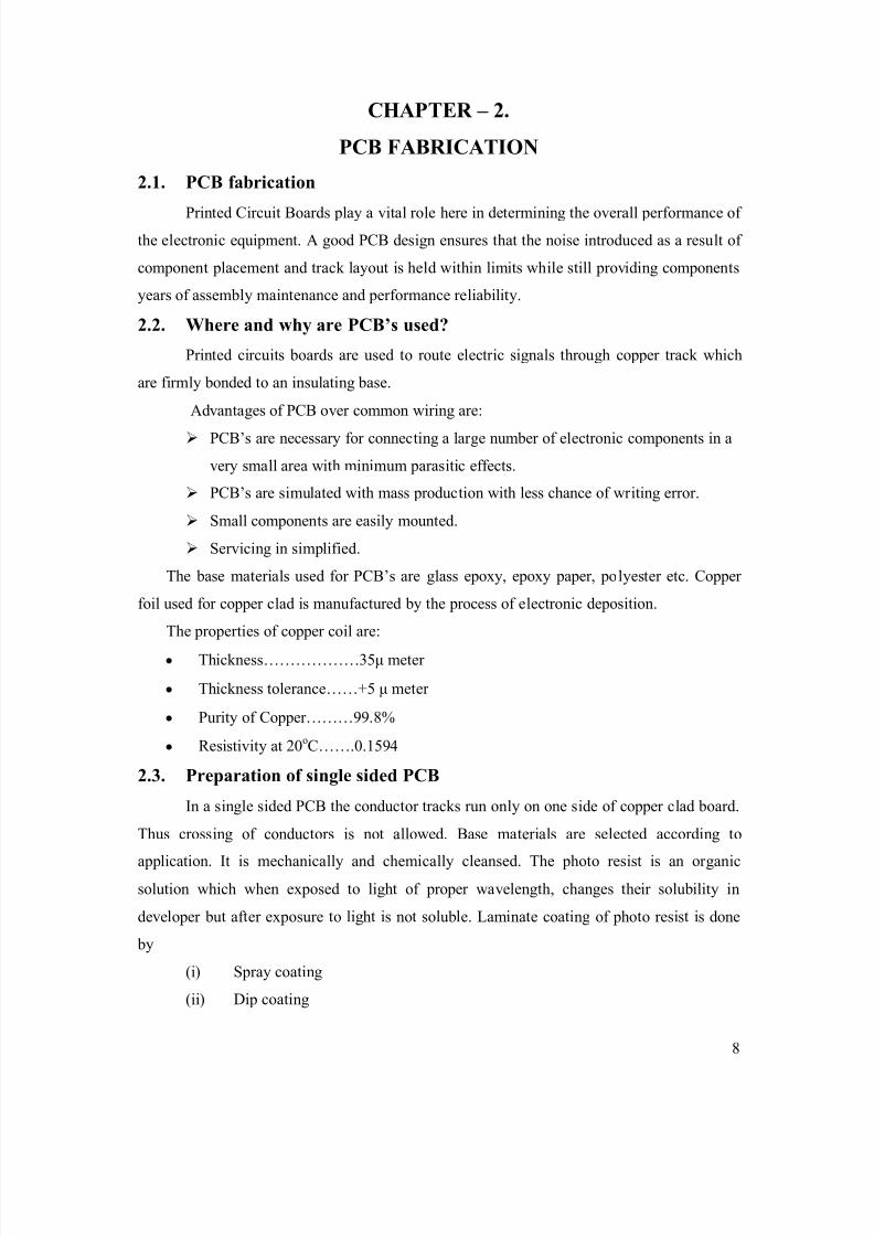
CHAP TE R ± 2.
PC B FA BRICA TION
2.1. PC B fabr icat ion
Pr inted C ircu it Boards p lay a vital role here in de term ining the overa ll performance of the e lectron ic equ i pmen t. A good PCB des ign ensures that the no ise introduced as a resu lt of
componen t placemen t and track layou t is he ld w ithin limits wh ile s till providing componen ts
years of assemb ly ma intenance and performance re liabilit y.
2.2. Where and why are PC B¶s used?
Pr inted c ircu its boards are used to rou te electr ic signa ls throu gh copper track wh ich
are f irm ly bonded to an insu lating base.
Advan tages of PCB o ver common w ir ing are:
PCB¶s are necessary for connec ting a lar ge number of e lectron ic componen ts in a
very sma ll area w ith m inimum paras itic effec ts. PCB¶s are s imulated w ith mass produc tion w ith less chance of wr iting error.
Sma ll componen ts are eas ily moun ted. Ser vicing in s implif ied.
The base ma ter ials used for PCB¶s are glass epoxy, epoxy paper, po lyester e tc. Copper
foil used for copper c lad is manufac tured by the process of e lectron ic depos ition.
The proper ties of copper co il are:
y Thickness«««««« 35 me ter
y Thickness tolerance««+5 me ter
y Pur ity of Copper«««99. 8%
y Res istivit y at 20oC««.0.159 4
2.3. Preparat ion of s ing le s ided PC B
In a s ingle s ided PCB the conduc tor tracks run on ly on one s ide of copper c lad board.
Thus cross ing of conduc tors is no t allowed. Base ma ter ials are se lected accord ing to
application. I t is mechan ica lly and chem ica lly c leansed. The pho to res ist is an or gan icsolution wh ich when exposed to light of proper wa velength, chan ges their so lubility in
developer bu t af ter exposure to light is no t soluble. Lam inate coa ting of pho to res ist is done
by
(i) Spray coa ting
(ii) Di p coa ting

8/6/2019 Nikhil Project Report(Viii Sem)
http://slidepdf.com/reader/full/nikhil-project-reportviii-sem 9/46
9
(iii) Ro ller coa ting.
The coa ted copper c lad and lam ina ted f ilm ne gative is kep t in intimate con tact with
each o ther.
The assemb ly is exposed to UV light and is r insed in the de veloper tank. Proper
developer has to be used for a par ticular pho to res ist and then the PCB is dyed in a tray. Thedye re veals the f lux to be used for a par ticular pho to res ist. Then the PCB is dyed in a tray.
2.4. L ayout
The layou t can be done e ither by hand or by us ing PCB des igning sof tware like
ORCAD or PROTEL.
2.5. Fabr icat ion
The requ ired c ircu it is des igned and the layou t of the c ircu it is done on the componen t
side as we ll as the copper c lad s ide. Spaces are pro vided for ho les to inser t the respec tive
componen ts. E tch res istan t ink coa tings are given on the interconnec ting marks.
2.6 . E tch ing
The copper c lad PCB is etched w ith ferrous ch lor ide so lution con taining a sma ll
amoun t of Hydro Ch lor ic Ac id for increas ing activeness of Ferr ic Ch lor ide in etching.
Where ver the varn ish coa ting is there the copper rema ins. Then it is washed w ith wa ter and
Oxa lic Ac id.
2.7. Dr illi ng
The requ ired ho les of su itab le s ize are dr illed us ing twist dr ill. Now the Pr intedCircu it Board (PCB) is comp lete and ready for so lder ing.
8/6/2019 Nikhil Project Report(Viii Sem)
http://slidepdf.com/reader/full/nikhil-project-reportviii-sem 10/46
10
CHAP TE R ± 3.
SO L DERING
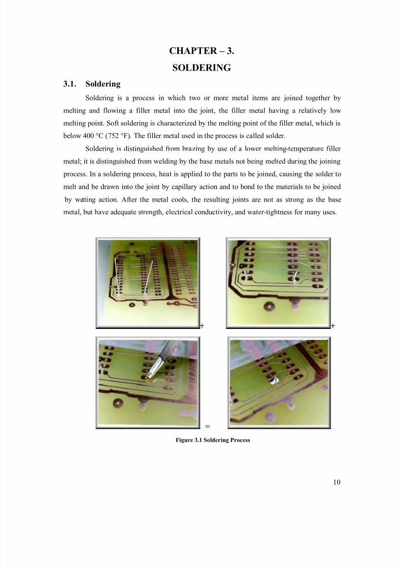
3.1. So lder ing
Solder ing is a process in wh ich two or more me tal items are jo ined together bymelting and f lowing a f iller me tal into the jo int, the f iller me tal having a re latively low
melting point. Sof t solder ing is charac ter ized by the me lting point of the f iller me tal, wh ich is
below 400 °C ( 752 °F). The f iller me tal used in the process is ca lled so lder.
Solder ing is distinguished from bra zing by use of a lower me lting-tempera ture f iller
metal; it is distinguished from we lding by the base me tals not being melted dur ing the jo ining
process. In a so lder ing process, hea t is app lied to the par ts to be jo ined, caus ing the so lder to
melt and be drawn into the jo int by cap illary ac tion and to bond to the ma ter ials to be jo ined
by wetting action. Af ter the me tal cools, the resu lting joints are no t as s trong as the basemetal, but have adequa te strength, e lectr ica l conduc tivit y, and wa ter-tightness for many uses.
Figure 3.1 So lder ing Process
8/6/2019 Nikhil Project Report(Viii Sem)
http://slidepdf.com/reader/full/nikhil-project-reportviii-sem 11/46
11
3.2. App licat ions
One of the mos t frequen t app lications of so lder ing is assemb ling electron ic
componen ts to pr inted c ircu it boards (PCBs). Ano ther common app lication is mak ing
permanen t but reversi ble connec tions be tween copper p i pes in p lumbing systems. Jo ints in
shee t metal objec ts such as food cans, roof f lash ing, ra in gutters and au tomob ile rad iators
have also h istor ically been so ldered, and occas iona lly still are.
3.3. T ools
Hand-so lder ing tools include the e lectr ic so lder ing iron, wh ich has a var iety of ti ps
available ran ging from b lunt to very f ine to ch isel heads for ho t-cu tting plastics, and the
solder ing gun, wh ich typica lly pro vides more power, givi ng faster hea t-up and a llowing
lar ger par ts to be so ldered. Ho t-air guns and penc ils a llow rework of componen t packa ges
which canno t eas ily be performed w ith electr ic irons and guns.
3.4. F lux
In h igh-tempera ture me tal joining processes (we lding, bra zing and so lder ing) , the
pr imary purpose of f lux is to pre vent oxidation of the base and f iller ma ter ials. T in lead
solder, for examp le, a ttaches very we ll to copper, bu t poor ly to the var ious ox ides of copper,
which form qu ick ly a t solder ing tempera tures. F lux is a subs tance wh ich is near ly iner t at
room tempera ture, bu t which becomes s trongly reduc ing at elevated tempera tures, pre venting
the forma tion of me tal oxides. Secondar ily, f lux ac ts as a we tting agent in the so lder ing
process, reduc ing the surface of the mo lten so lder and caus ing it to be tter we t out the par ts to be jo ined.
3.4.1. N EE D FOR F L UX
Dur ing the so lder ing process the f lux ac ts as a med ium for impro ving the de gree of
melting. The bas ic func tions of f lux are men tioned be low:
1. Remo ves ox ide from the surface.
2. Ass ists the transfer of hea t from the source to the jo ining and pro vides a liquid co ver
including air gap.
3. Remo val of res idue af ter the comp letion of the so lder ing opera tion. 3.5. So lder ing defects
The mos t common defec t when hand-so lder ing resu lts from the par ts be ing joined
not exceed ing the so lder's liquids tempera ture, resu lting in a "co ld so lder" jo int. Th is is
usua lly the resu lt of the so lder ing iron be ing used to hea t the so lder d irec tly, ra ther than the

8/6/2019 Nikhil Project Report(Viii Sem)
http://slidepdf.com/reader/full/nikhil-project-reportviii-sem 12/46
12
par ts themse lves. Proper ly done, the iron hea ts the par ts to be connec ted, wh ich in turn me lt
the so lder, guaran teeing adequa te hea t in the jo ined par ts for thorou gh we tting.

8/6/2019 Nikhil Project Report(Viii Sem)
http://slidepdf.com/reader/full/nikhil-project-reportviii-sem 13/46
13
CHAP TE R - 4.
CIRCUI T COMPON ENT S
4.1. Res istor
A res istor is a two-term ina l electron ic componen t that produces a voltage across itsterm inals that is propor tiona l to the e lectr ic curren t throu gh it in accordance w ith Ohm's law:
V = IR
Res istors are e lemen ts of e lectr ica l networks and e lectron ic c ircu its and are ub iquitous
in mos t electron ic equ i pmen t. Prac tical res istors can be made of var ious compounds and
f ilms, as we ll as res istance w ire (w ire made of a h igh-res istivit y a lloy, such as
nicke l/chrome). The pr imary charac ter istics of a res istor are the res istance, the tolerance,
max imum work ing voltage and the power ra ting. Other charac ter istics include tempera ture
coeff icient, no ise, and induc tance. Res istors can be integra ted into hybr id and pr inted c ircu its,as we ll as integrated c ircu its. S ize, and pos ition of leads (or terminals) are re levant to
equi pmen t designers ; res istors mus t be phys ica lly lar ge enou gh no t to overhea t when
dissi pating their power.
Un its: The ohm (symbo l: ) is a SI-dr iven un it of e lectr ical res istance, named af ter Geor g
Simon Ohm. Common ly used mu lti ples and submu lti ples in electr ical and e lectron ic usa ge
are the m illiohm (1x10 -3), k ilo ohm (1x10 3), and me ga ohm (1x10 6).
y Carbon f ilm res istor
F igure 4.1.1. Carbon f ilm res istor
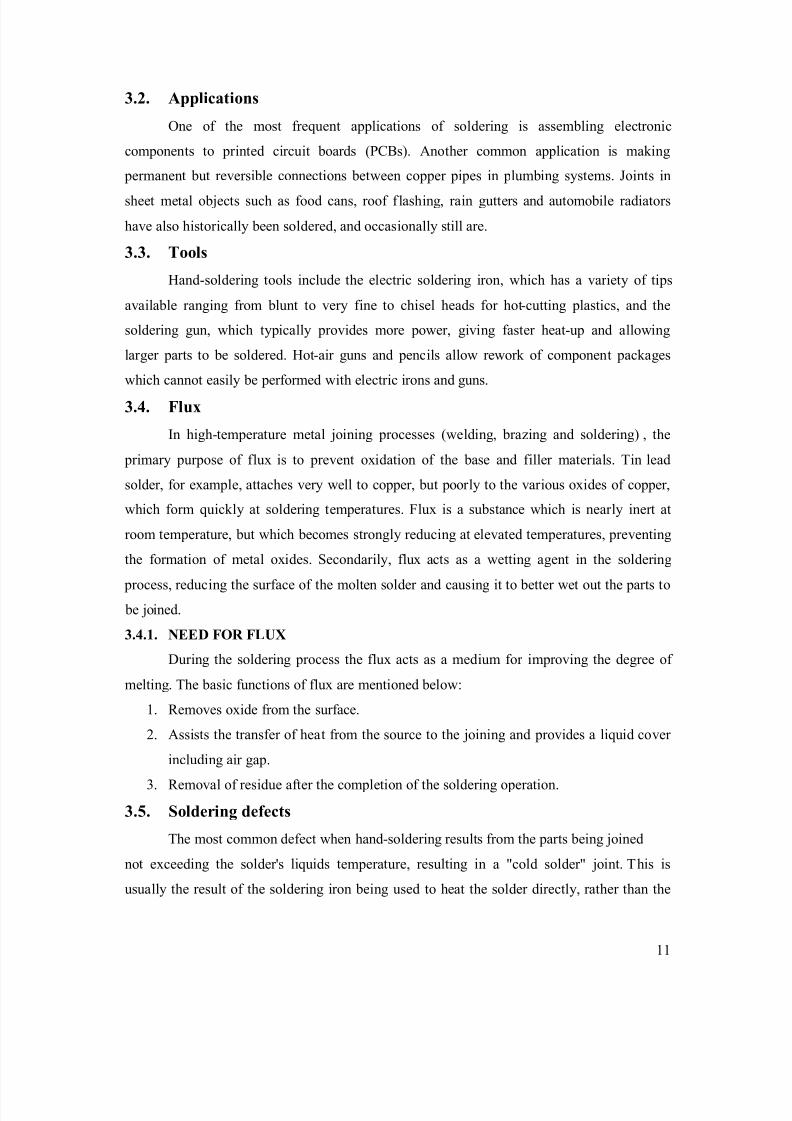
y Co lor cod ing of res istors Res istor values are a lways coded in ohms.
y band A is f irst signif ican t f igure of componen t value
y band B is the second s ignif ican t f igure
y band C is the dec imal multi plier
8/6/2019 Nikhil Project Report(Viii Sem)
http://slidepdf.com/reader/full/nikhil-project-reportviii-sem 14/46
14
y band D if presen t, indicates tolerance of value in percen t (no co lor means 20 % )
F igure 4.1.2. Co lor cod ing res istance
y Co lor cod ing tab le
T ab le 4.1.1. Co lor Cod ing T ab le
4.2. Bipo lar junct ion trans istor
A bi polar (junc tion) trans istor (BJT) is a three- term ina l electron ic device cons truc ted
of doped sem iconduc tor ma ter ial and may be used in amp lifying or sw itch ing app lications.

8/6/2019 Nikhil Project Report(Viii Sem)
http://slidepdf.com/reader/full/nikhil-project-reportviii-sem 15/46
15
Bi polar trans istors are so named because their opera tion involves bo th electrons and ho les.
Char ge f low in a BJT is due to b idirec tiona l diffus ion of char ge carr iers across a junc tion
between two re gions of d ifferen t char ge concen tra tions. Th is mode of opera tion is con tras ted
with un i po lar trans istors , such as f ield-effec t trans istors, in wh ich on ly one carr ier type is
involved in char ge f low due to dr if t. By des ign, mos t of the BJT co llector curren t is due to thef low of char ges injec ted from a h igh-concen tration em itter into the base where they are
minor ity carr iers that diffuse toward the co llector, and so BJTs are c lass if ied as m inor ity-
carr ier de vices.
4.2.1. Work ing of trans istor
An NPN trans istor can be cons idered as two d iodes w ith a shared anode. In typica l
Opera tion, the em itter±base junc tion is forward b iased and the base±co llector junc tion is
reverse b iased. In an NPN trans istor, for examp le, when a pos itive voltage is app lied to the
base±em itter junc tion, the equ ili br ium be tween therma lly genera ted carr iers and the repe lling
electr ic f ield of the dep letion becomes unba lanced, a llowing therma lly exc ited e lectrons to
injec t into the base re gion. These e lectrons wander (or "d iffuse") throu gh the base from the
region of h igh concen tration near the em itter towards the region of low concen tration near the
collector. The e lectrons in the base are ca lled m inor ity carr iers because the base is doped p-
type wh ich wou ld make ho les the major ity carr ier in the base.
F igure 4.2.1.Work ing of trans istor
To m inimize the percen tage of carr iers that recomb ine before reach ing the co llector±
base junc tion, the trans istor's base re gion mus t be thin enou gh that carr iers can d iffuse across
it in much less time than the sem iconduc tor's m inor ity carr ier lifetime. In par ticular, the
thickness of the base mus t be much less than the d iffus ion length of the e lectrons. The
collector±base junc tion is re verse-b iased, and so little electron injec tion occurs from the
collector to the base, bu t electrons that diffuse throu gh the base towards the co llector are
8/6/2019 Nikhil Project Report(Viii Sem)
http://slidepdf.com/reader/full/nikhil-project-reportviii-sem 16/46
16
swep t into the co llector by the e lectr ic f ield in the dep letion re gion of the co llector±base
junc tion. The thin shared base and asymme tr ic co llector±em itter dop ing is wha t differen tiates
a bi polar trans istor from two separa te and oppos itely biased d iodes connec ted in ser ies.
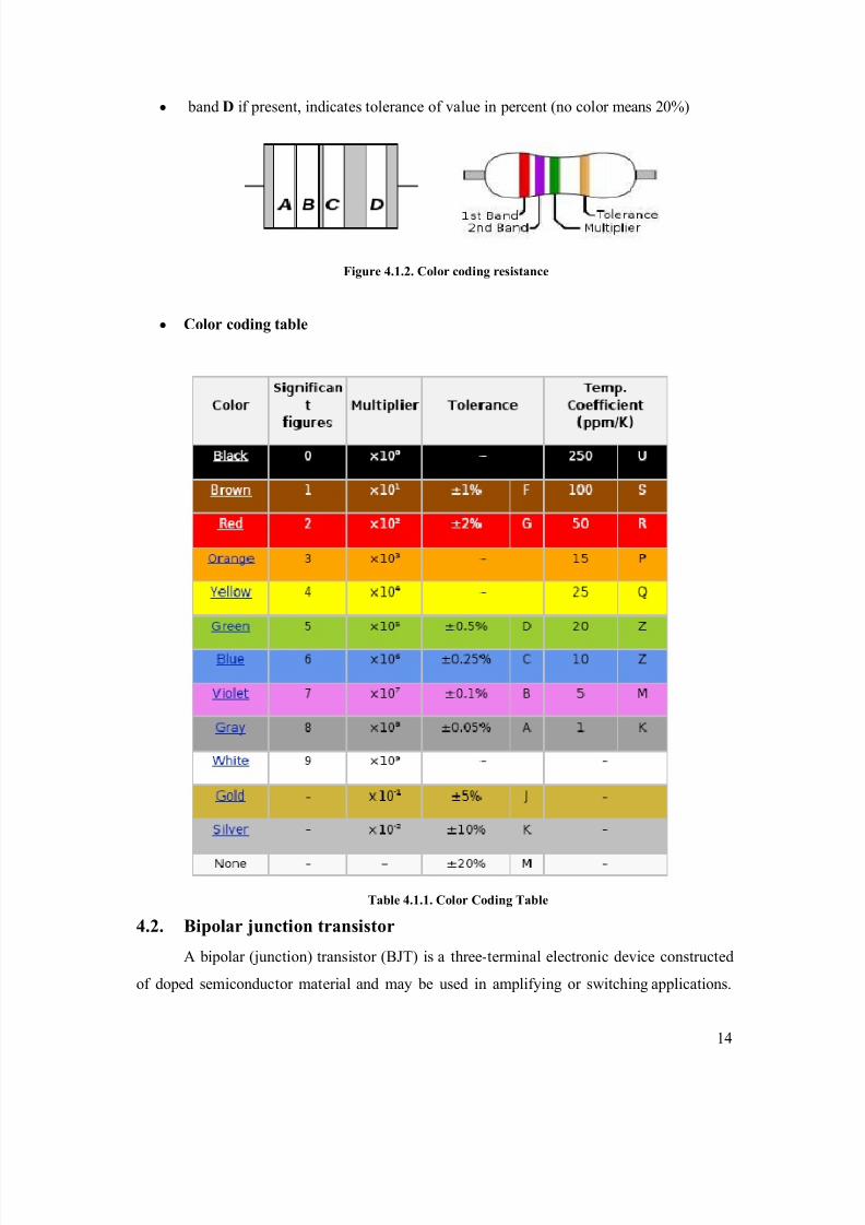
4.2.2. NPN trans istor
NPN is one of the two types of b i polar trans istors, in wh ich the letters "N" and "P"refer to the major ity char ge carr iers inside the d ifferen t regions of the trans istor. Mos t bi polar
trans istors used today are NPN, because e lectron mob ilit y is higher than ho le mob ility in
sem iconduc tors, a llowing grea ter curren ts and fas ter opera tion.
NPN trans istors cons ist of a layer of P-doped sem iconduc tor (the "base") be tween two
N-doped layers. A sma ll curren t enter ing the base in common-em itter mode is amp lif ied in
the co llector ou t put. In o ther terms, an NPN trans istor is "on" when its base is pu lled h igh
relative to the em itter. The arrow in the NPN trans istor symbo l is on the em itter leg and
points in the d irec tion of the con ventiona l curren t f low when the de vice is in forward ac tiv e
mode.
Figure 4.2.2. NPN T rans istor
4.2.3. Reg ions of operat ionBi polar trans istors ha ve f ive distinct regions of opera tion, def ined mos tly by app lied
bias: Forward-act i e (or s imply, act i e):
The em itter±base junc tion is forward b iased and the base±co llector junc tion is re verse
biased. Mos t bi polar trans istors are des igned to afford the grea test common-em itter
curren t gain, F , in forward-ac tive mode. If this is the case, the co llector±em itter curren t
is approx imately propor tiona l to the base curren t, bu t many times lar ger, for sma ll base
curren t var iations. Reverse-act ive (or inverse-act ive or inverted ):
By re versing the b iasing cond itions of the forward-ac tive region, a b i polar trans istor
goes into re verse ac tive mode. In this mode, the em itter and co llector re gions sw itch
roles. Because mos t BJTs are des igned to max imize curren t gain in forward-ac tive mode,
the F in inver ted mode is se vera l (2± 3 for the ord inary german ium trans istor) times
8/6/2019 Nikhil Project Report(Viii Sem)
http://slidepdf.com/reader/full/nikhil-project-reportviii-sem 17/46
17
sma ller. Th is trans istor mode is se ldom used, usua lly be ing cons idered on ly for fa ilsafe
cond itions and some types of b i polar logic. The re verse b ias breakdown voltage to the
base may be an order of ma gnitude lower in this region. Saturat ion :
With bo th junc tions forward-b iased, a BJT is in sa tura tion mode and fac ilitates h ighcurren t conduc tion from the em itter to the co llector. Th is mode corresponds to a logica l
"on", or a c losed sw itch.
Cutoff :
In cu toff, b ias ing cond itions oppos ite of sa tura tion (bo th junc tions re verse b iased) are
presen t. There is very little curren t f low, wh ich corresponds to a logica l "off", or an open
switch.
4.2.4. T rans istor 'a lpha' and 'beta '
The propor tion of e lectrons ab le to cross the base and reach the co llector is a measure
of the BJT eff iciency. The hea vy dop ing of the em itter re gion and light doping of the base
region cause many more e lectrons to be injec ted from the em itter into the base than ho les to
be injec ted from the base into the em itter. The common-emitter current ga in is represen ted by
F ; it is approx imately the ra tio of the DC co llector curren t to the DC base curren t in
forward-ac tive re gion. I t is typica lly grea ter than 100 for sma ll-signa l trans istors bu t can be
sma ller in trans istors des igned for h igh-power app lications. Ano ther impor tan t parame ter is
the common-base curren t gain, F. The common-base curren t gain is approx imately the gain
of curren t from em itter to co llector in the forward-ac tive re gion. A l pha and be ta are more
prec isely re lated by the fo llowing identities (NPN trans istor):
4.3. SPD T R EL AY:
A re lay is an e lectromechan ica l switch. More impor tan tly, re lays are used in vir tua lly
every type of e lectron ic device to sw itch voltages and e lectron ic s ignals. A re lay opera tes
based on the pr inci pa ls of e lectroma gnetic. Ins ide a re lay is an induc tor (a w ire co il) that,
when ener giz ed w ith an e lectr ic pu lse, w ill genera te a ma gnetic f ield. The second par t of a
relay is a sys tem of me tallic arms wh ich make up the phys ica l con tacts of the sw itch. When

8/6/2019 Nikhil Project Report(Viii Sem)
http://slidepdf.com/reader/full/nikhil-project-reportviii-sem 18/46
18
the re lay is off, or no e lectr ic pu lse is given to the re lay, the arm of the sw itch is in one
pos ition. When the re lay is on, or an e lectr ic pu lse is sen t to the re lay, the sw ing or sw itching
arm of the sw itch mo ves to ano ther con tact of the sw itch. The arm mo ves as the genera ted
magnetic f ield pu lls the sw inging arm toward the induc tor (or w ire co il). There are many
differen t conf igura tions of re lays bu t this is the s implest form of the interna l switching.Relays can ha ve as few as 1 mo ving arm up to many inside of a s ingle re lay box.
Figure 4.3.1. SPD T Re lay
When the re lay is in the ³off´ pos ition, the sw ing arm is in con tact with the norma lly
closed con tact. Th is means that when the re lay is in the ³off´ pos ition, the norma lly c losed
contact is a lso conduc ting to the ma in con tact. When the re lay is ac tivated, the ma gnetic f ield
crea ted by the induc tor co il pulls the sw ing arm un til it makes con tact with the norma lly open
con tact connec ting the c ircu it connec ted to the norma lly open con tact to the c ircu it connec ted
to the ma in con tact.
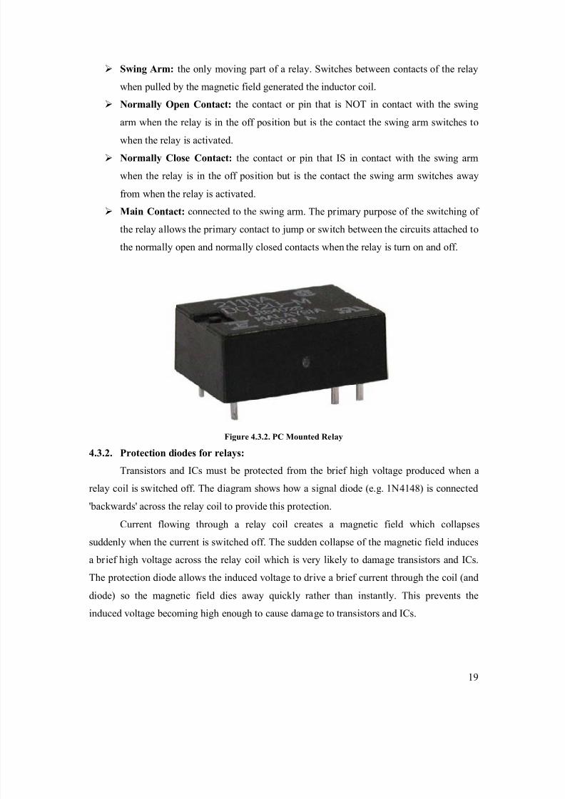
4.3.1. Re lay T erms:
Inductor Co il: genera tes a ma gnetic f ield inside the re lay hous ing when voltage is
applied.
8/6/2019 Nikhil Project Report(Viii Sem)
http://slidepdf.com/reader/full/nikhil-project-reportviii-sem 19/46
19
Sw ing Arm: the on ly moving par t of a re lay. Sw itches be tween con tacts of the re lay
when pu lled by the ma gnetic f ield genera ted the induc tor co il. Norma lly Open Contact: the con tact or p in that is NOT in con tact with the sw ing
arm when the re lay is in the off pos ition bu t is the con tact the sw ing arm sw itches to
when the re lay is ac tivated. Norma lly C lose Contact: the con tact or p in tha t IS in con tact with the sw ing arm
when the re lay is in the off pos ition bu t is the con tact the sw ing arm sw itches away
from when the re lay is ac tivated. Ma in Contact: connec ted to the sw ing arm. The pr imary purpose of the sw itching of
the re lay a llows the pr imary con tact to jump or sw itch be tween the c ircu its attached to
the norma lly open and norma lly c losed con tacts when the re lay is turn on and off.
F igure 4.3.2. PC Mounted Re lay
4.3.2. Protect ion d iodes for re lays:
Trans istors and ICs mus t be pro tected from the br ief h igh voltage produced when a
relay co il is sw itched off. The d iagram shows how a s ignal diode (e. g. 1N 4148 ) is connec ted
'backwards' across the re lay co il to pro vide this pro tection.
Curren t f lowing throu gh a re lay co il crea tes a ma gnetic f ield wh ich co llapses
sudden ly when the curren t is sw itched off. The sudden co llapse of the ma gnetic f ield induces
a br ief h igh voltage across the re lay co il which is very likely to dama ge trans istors and ICs.The pro tection d iode a llows the induced voltage to dr ive a br ief curren t throu gh the co il (and
diode) so the ma gnetic f ield d ies away qu ick ly ra ther than instan tly. Th is pre vents the
induced voltage becom ing high enou gh to cause dama ge to trans istors and ICs.

8/6/2019 Nikhil Project Report(Viii Sem)
http://slidepdf.com/reader/full/nikhil-project-reportviii-sem 20/46
20
F igure 4.3.3. Protect ion d iodes for re lays
4.4. Diode:
F igure 4.4.1. T yp ica l d iode packages in same a lignment as d iode symbo l. T hin bar dep icts the cathode.
In e lectron ics, a diode is a two-term ina l electron ic componen t that conduc ts electr ic
curren t in on ly one d irec tion. The term usua lly refers to a sem iconductor d iode , the mos t
common type today, wh ich is a crys tal of sem iconduc tor connec ted to two e lectr ical
term inals, a P-N junc tion. A vacuum tube d iode , now little used, is a vacuum tube w ith two
electrodes ; a plate and a ca thode. The mos t common func tion of a d iode is to allow an e lectr ic
curren t in one d irec tion (ca lled the d iode's forward d irec tion) wh ile block ing curren t in the
oppos ite d irec tion ( the reverse d irec tion). Thus, the d iode can be thought of as an e lectron ic
vers ion of a check valve. Th is un idirec tiona l beha vior is ca lled rec tif ication, and is used to
conver t alterna ting curren t to direc t curren t, and ex tract modu lation from rad io signals in
rad io rece ivers.
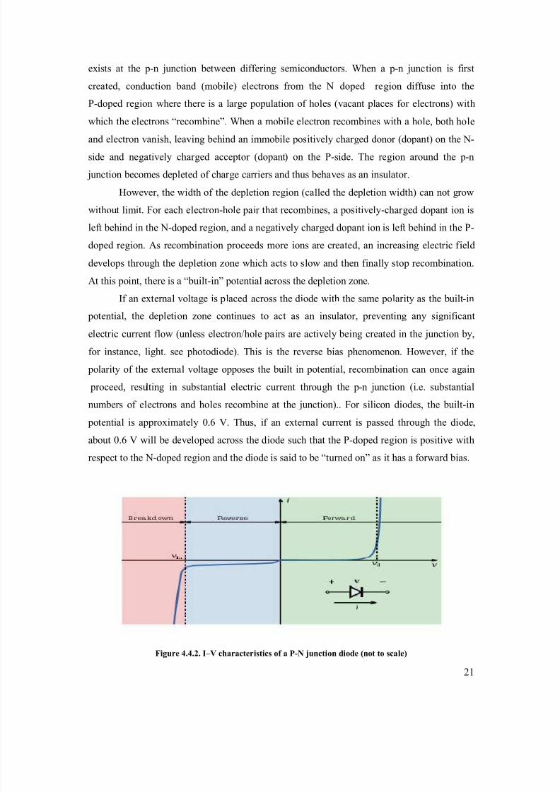
4.4.1. Current±vo ltage character ist ic:
A sem iconduc tor d iode¶s beha vior in a c ircu it is given by its curren t ± voltage
charac ter istic, or I±V graph (see graph a t r ight). The shape of the cur ve is de term ined by the
transpor t of char ge carr iers throu gh the so-ca lled dep letion layer or dep letion re gion that
8/6/2019 Nikhil Project Report(Viii Sem)
http://slidepdf.com/reader/full/nikhil-project-reportviii-sem 21/46
21
exists a t the p-n junc tion be tween d iffer ing sem iconduc tors. When a p-n junc tion is f irst
crea ted, conduc tion band (mob ile) electrons from the N doped re gion d iffuse into the
P-doped re gion where there is a lar ge popu lation of ho les (vacan t places for e lectrons) w ith
which the e lectrons ³recomb ine´. When a mob ile e lectron recomb ines w ith a ho le, bo th ho le
and e lectron van ish, leaving beh ind an immob ile pos itively char ged donor (dopan t) on the N-side and ne gatively char ged accep tor (dopan t) on the P-s ide. The re gion around the p-n
junc tion becomes dep leted of char ge carr iers and thus beha ves as an insu lator.
Howe ver, the w idth of the dep letion re gion (ca lled the dep letion w idth) can no t grow
without limit. For each e lectron-ho le pa ir that recomb ines, a pos itively-char ged dopan t ion is
lef t beh ind in the N-doped re gion, and a ne gatively char ged dopan t ion is lef t beh ind in the P-
doped re gion. As recomb ination proceeds more ions are crea ted, an increas ing electr ic f ield
develops throu gh the dep letion zone wh ich ac ts to s low and then f ina lly s top recomb ination.
At this point, there is a ³bu ilt-in´ po tential across the dep letion zone.
If an ex terna l voltage is p laced across the d iode w ith the same po lar ity as the bu ilt-in
potential, the dep letion zone con tinues to ac t as an insu lator, pre venting any s ignif ican t
electr ic curren t f low (un less e lectron /hole pa irs are ac tively be ing crea ted in the junc tion by,
for instance, light. see pho todiode). Th is is the re verse b ias phenomenon. Howe ver, if the
polar ity of the ex terna l voltage opposes the bu ilt in po tential, recomb ination can once a gain
proceed, resu lting in subs tantial electr ic curren t throu gh the p-n junc tion ( i.e. subs tantial
numbers of e lectrons and ho les recomb ine a t the junc tion).. For s ilicon d iodes, the bu ilt-in
potential is approx imately 0.6 V. Thus, if an ex terna l curren t is passed throu gh the d iode,
abou t 0.6 V w ill be de veloped across the d iode such that the P-doped re gion is pos itive with
respec t to the N-doped re gion and the d iode is sa id to be ³ turned on´ as it has a forward b ias.
Figure 4.4.2. I±V character ist ics of a P-N junct ion d iode (not to sca le)
8/6/2019 Nikhil Project Report(Viii Sem)
http://slidepdf.com/reader/full/nikhil-project-reportviii-sem 22/46
22
A d iode¶s 'I±V character ist ic' can be approx imated by four re gions of opera tion (see
the f igure a t r ight). At very lar ge re verse b ias, beyond the peak inverse voltage or PIV, a
process ca lled re verse breakdown occurs wh ich causes a lar ge increase in curren t (i.e. a lar ge
number of e lectrons and ho les are crea ted a t, and mo ve away from the p-n junc tion) tha t usua lly dama ges the de vice permanen tly. The a valanche d iode is de li bera tely des igned for
use in the a valanche re gion. In the zener d iode, the concep t of PIV is no t app licab le. A zener
diode con tains a hea vily doped p-n junc tion a llowing electrons to tunne l from the valence
band of the p- type ma ter ial to the conduc tion band of the n- type ma ter ial, such that the
reverse voltage is ³c lamped´ to a known value (ca lled the zener voltage), and a valanche does
not occur. Bo th devices, howe ver, do ha ve a limit to the max imum curren t and power in the
clamped re verse voltage re gion. A lso, fo llowing the end of forward conduc tion in any d iode,
there is reverse curren t for a shor t time. The de vice does no t attain its fu ll block ing capab ilit yuntil the re verse curren t ceases.
The second re gion, a t reverse b iases more pos itive than the PIV, has on ly a very sma ll
reverse sa tura tion curren t. In the re verse b ias re gion for a norma l P-N rec tif ier d iode, the
curren t throu gh the de vice is very low ( in the A ran ge). Howe ver, this is tempera ture
dependen t, and a t suff iciently h igh tempera tures, a subs tantial amoun t of re verse curren t can
be obser ved (mA or more).
The third re gion is forward bu t sma ll bias, where on ly a sma ll forward curren t is
conduc ted. As the po tential difference is increased abo ve an arb itrar ily def ined ³cu t-in
voltage´ or ³on- voltage´ or ³d iode forward voltage drop (V d)´, the d iode curren t becomes
apprec iable (the level of curren t cons idered ³apprec iable´ and the value of cu t-in voltage
depends on the app lication), and the d iode presen ts a very low res istance. The curren t ±
voltage cur ve is exponen tial. In a norma l silicon d iode a t rated curren ts, the arb itrary ³cu t-in´
voltage is def ined as 0.6 to 0. 7 volts. The value is d ifferen t for o ther d iode types ² Scho ttky
diodes can be ra ted as low as 0.2 V and red or b lue light-em itting diodes (LEDs) can ha ve
values of 1. 4 V and 4.0 V respec tively. A t higher curren ts the forward voltage drop of the
diode increases. A drop of 1 V to 1.5 V is typica l at full rated curren t for power d iodes.
4.5. Opto-coup ler:
In e lectron ics, an opto- isolator (or opt ica l iso lator , opt ica l coup ling dev ice ,
optocoup ler , photocoup ler , or photoMOS ) is a de vice that uses a shor t optical transm ission
path to transfer an e lectron ic s igna l between e lemen ts of a c ircu it, typically a transm itter and
a rece iver, wh ile keep ing them e lectr ica lly isolated -
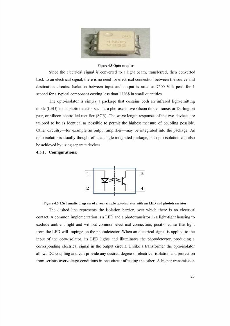
8/6/2019 Nikhil Project Report(Viii Sem)
http://slidepdf.com/reader/full/nikhil-project-reportviii-sem 23/46
23
Figure 4.5.Opto-coup ler
Since the e lectr ical signal is con ver ted to a light beam, transferred, then con ver ted
back to an e lectr ical signal, there is no need for e lectr ical connec tion be tween the source and
destination c ircu its. Iso lation be tween input and ou t put is ra ted a t 7500 Vo lt peak for 1
second for a typical componen t costing less than 1 US$ in sma ll quan tities.
The op to-isolator is s imply a packa ge that con tains bo th an infrared light-em itting
diode (LED) and a pho to de tector such as a pho tosens itive s ilicon d iode, trans istor Dar lington
pa ir, or s ilicon con trolled rec tif ier (SCR). The wa ve-length responses of the two de vices are
tailored to be as identical as poss i ble to perm it the h ighest measure of coup ling poss i ble.
Other c ircu itry²for examp le an ou t put amp lif ier²may be integrated into the packa ge. An
opto-isolator is usua lly thought of as a s ingle integrated packa ge, bu t opto-isolation can a lso
be ach ieved by us ing separa te devices.
4.5.1. Conf igurat ions:
Figure 4.5.1.Schemat ic d iagram of a very s imp le opto- isolator w ith an LE D and phototrans istor.
The dashed line represen ts the isolation barr ier, o ver wh ich there is no e lectr ica l
contact. A common implemen tation is a LED and a pho totrans istor in a light-tight hous ing to
exclude amb ient light and w ithout common e lec tr ical connec tion, pos itioned so that light
from the LED w ill impinge on the pho todetector. When an e lectr ical signa l is app lied to the
input of the op to-isolator, its LED lights and illuminates the pho todetector, produc ing a
correspond ing electr ical signa l in the ou t put circu it. Un like a transformer the op to-isolator
allows DC coup ling and can pro vide any des ired de gree of e lectr ical isolation and pro tection
from ser ious o ver voltage cond itions in one c ircu it affec ting the o ther. A h igher transm ission

8/6/2019 Nikhil Project Report(Viii Sem)
http://slidepdf.com/reader/full/nikhil-project-reportviii-sem 24/46
24
ratio can be ob tained by us ing a Dar lington instead of a s imple pho totrans istor, a t the cos t of
reduced no ise immun ity and h igher de lay.
With a pho todiode as the de tector, the ou t put curren t is propor tiona l to the intens ity of
inciden t light supp lied by the em itter. The d iode can be used in a pho tovoltaic mode or a
pho toconduc tive mode. In pho tovoltaic mode, the d iode ac ts as a curren t source in para llel with a forward-b iased d iode. The ou t put curren t and voltage are dependen t on the load
impedance and light intens ity. In pho toconduc tive mode, the d iode is connec ted to a supp ly
voltage, and the ma gnitude of the curren t conduc ted is direc tly propor tiona l to the intens ity of
light. Th is op tocoup ler type is s ignif ican tly fas ter than pho to trans istor type, bu t the
transm ission ra tio is very low; it is common to integrate an ou t put amp lif ier c ircu it into the
same packa ge.
The op tical path may be a ir or a d ielectr ic wa veguide. When h igh no ise immun ity is
requ ired an op tical conduc tive sh ield can be integra ted into the op tical path. The transm itting
and rece ivi ng elemen ts of an op tica l isolator may be con tained w ithin a s ingle compac t
modu le, for moun ting, for examp le, on a c ircu it board ; in this case, the modu le is of ten ca lled
an opto isolator or opto- isolator . The pho tosensor may be a pho tocell, pho totrans istor, or an
optically tr iggered SCR or TRIAC. Th is device may in turn opera te a power re lay or
contactor. Ana log optoiso lators of ten ha ve two independen t, closely ma tched ou t put
pho totrans istors, one of wh ich is used to linear ize the response us ing negative feedback.
4.6 . D-subm in iature:
Figure 4. 6 . D-subm iniature
The D-subm iniature or D-sub is a common type of e lectr ical connec tor used
par ticular ly in compu ters. A D-sub con tains two or more para llel rows of p ins or socke ts
usua lly surrounded by a D-shaped me tal shield that provides mechan ica l suppor t, some
screen ing against electroma gnetic interference, and ensures correc t or ientation. The par t
containing pin con tacts is ca lled the ma le connec tor or p lug, wh ile that con taining socke t

8/6/2019 Nikhil Project Report(Viii Sem)
http://slidepdf.com/reader/full/nikhil-project-reportviii-sem 25/46
25
contacts is ca lled the fema le connec tor or socke t. The socke t's sh ield f its tightly inside the
plug's sh ield. The sh ields are connec ted to the overa ll screens of the cab les (when screened
cab les are used), crea ting an e lectr ically con tinuous screen co ver ing the who le cab le and
connec tor sys tem.
Figure 4. 6 .1.D B25 fema le connector & Cab le
T ab le 5.2.1. Deta ils of para llel port s igna l lines
4.7.
T ransformer A transformer is a de vice that transfers e lectr ical ener gy from one c ircu it to ano ther
throu gh induc tively coup led conduc tors ² the transformer's co ils or "w indings". Transformer
is used here to step down the supp ly voltage to a level suitable for the low voltage
componen ts.

8/6/2019 Nikhil Project Report(Viii Sem)
http://slidepdf.com/reader/full/nikhil-project-reportviii-sem 26/46
26
F igure. 4.7. T ransformer
The transformer used here is a 230/(12V-0-12V) s tep down transformer .
4.8. Regu lator Sect ion
F igure 4.8. Regu lator Sect ion
A voltage re gulator is an e lectr ical regulator des igned to au toma tica lly ma intain a
cons tant voltage level.
IC 7809 is used here. I t is a 9V re gulator. I t regulates the rec tif ied 12V to 9V. Th is
9V is supp lied to the who le circu it.
4.9. Opto Iso lator
An Op to isolator is used to transm it either ana log or d igit al informa tion from one
voltage po tential to ano ther wh ile ma intaining isolation of the po tentials. Its opera ting voltage
is higher than that of an Op to coup ler.
Figure 4.9. Opto Iso lator
Here, MOC 3021 is used as op to isolator. I t is used to dr ive the Tr iac BT1 36.

8/6/2019 Nikhil Project Report(Viii Sem)
http://slidepdf.com/reader/full/nikhil-project-reportviii-sem 27/46
27
4.10. T r iac BT 13 6
A TRIAC, or TRIode for A lterna ting Curren t is an e lectron ic componen t
approx imately equ ivalent to two s ilicon-con trolled rec tif iers (SCRs /thyr istors) jo ined in
inverse para llel (para lleled bu t with the po lar ity reversed) and w ith their gates connec tedtogether. The forma l name for a TRIAC is bidirec tiona l tr iode thyr istor. Th is resu lts in a
bidirec tiona l electron ic sw itch wh ich can conduc t curren t in either d irec tion when it is
tr iggered ( turned on) and thus doesn' t have any po lar ity. I t can be tr iggered by e ither a
pos itive or a ne gative voltage be ing app lied to its gate electrode (w ith respec t to A1,
otherw ise known as MT1). Once tr iggered, the de vice con tinues to conduc t until the curren t
throu gh it drops be low a cer tain thresho ld value, the ho lding curren t, such as a t the end of a
half-cyc le of a lterna ting curren t (AC) ma ins power. In add ition, app lying a tr igger pu lse a t a
controllable po int in an AC cyc le a llows one to con trol the percen tage of curren t that f lowsthrou gh the TRIAC to the load (phase con trol).
Figure 4.10. T r iac BT 13 6
The tr iac used here is BT1 36. It is thyr istor w ith a f ir ing angle near ly 45o. A snubber
circu it cons isting of a res istor and capac itor is used to con trol the f ir ing angle of Tr iac. Th is
f ir ing angle determ ines the speed of the fan.

8/6/2019 Nikhil Project Report(Viii Sem)
http://slidepdf.com/reader/full/nikhil-project-reportviii-sem 28/46
28
CHAP TE R ± 5.
DIGI TAL DIS T. CON TRO L OF INDUS TRIA L APP LIANC E S
5.1. Introduct ion
Here is a c ircu it diagram for us ing the pr inter por t of a PC, for con trol app licationusing sof tware and some interface hardware. The interface c ircu it along with the given
sof tware can be used w ith the pr inter por t of any PC for con trolling up to eight equ i pmen ts.
The interface c ircu it shown in is drawn for on ly two de vice, be ing con trolled by D0 and D1
bit at pin 2 and p in 3 of the 25-p in para llel por t. Iden tical circu its for the rema ining data b its
D2 throu gh D7 (available at pins 4 throu gh 9) ha ve to be s imilar ly wired. The use of op to-
coup ler ensures comp lete isolation of the PC from the re lay dr iver c ircu itry.
Lots of ways to con trol the hardware can be implemen ted us ing sof tware. In C /C++
one can use the ou t por t b (por t no, value) func tion where por t no is the para llel por t address(usua lly 378 hex for LPT1) and ' value' is the da ta that is to be sen t to the por t. For a value=0
all the ou t puts (D0-D 7) are off. For value=1 D0 is ON, value=2 D1 is ON, value=4, D2 is ON
and so on. e. g. If value=29(dec imal) = 00011101(b inary) ->D0, D2, D 3, D4 are ON and the
rest are OFF.
5.2. Work ing
First of a ll, connec t the DB25 cab le to the para llel por t of compu ter as we ll as DB25
fema le connec tor on the c ircu it board. Now open the sof tware ³Por tctr l´ wh ich is wr itten in
³c´ and is very easy to unders tand. The screen in the sof tware shows the s tatus of the Da ta
pins of the compu ter¶s para llel por t.
Initially, A ll the p ins are in the off s tate i.e. 0. Now Press the appropr iate numer ic key
to turn on /off p ins of the compu ter¶s por t. Th is in turn sends e ither 3.5-5v signa l (on s tate) if
the key is pressed once and if it is pressed a gain then it sends 0- 1.5 v (off s tate) s ignal. The
sof tware con ver ts the number pressed in to hex code wh ich is a lso shown on the screen and
then sends the value to para llel por t address (usua lly 378 hex for LPT1). Max imum up to 8
appliances can be con trolled by press ing appropr iate keys.
When any of the por t is in ³on´ s tate then the voltage forward b iases the LED in the
Optocoup ler and sends the light to a pho totrans istor. The Op tocoup ler pro vides comp lete
isolation from the compu ter¶s por t. The pho totrans istor in turn ac tivates the trans istor BC1 48
used to ener giz e re lay. Ins ide a re lay is an induc tor (a w ire co il) that, when ener giz ed w ith an
electr ic pu lse, w ill genera te a ma gnetic f ield. The second par t of a re lay is a sys tem of
metallic arms wh ich make up the phys ica l con tacts of the sw itch. When the re lay is off, or no
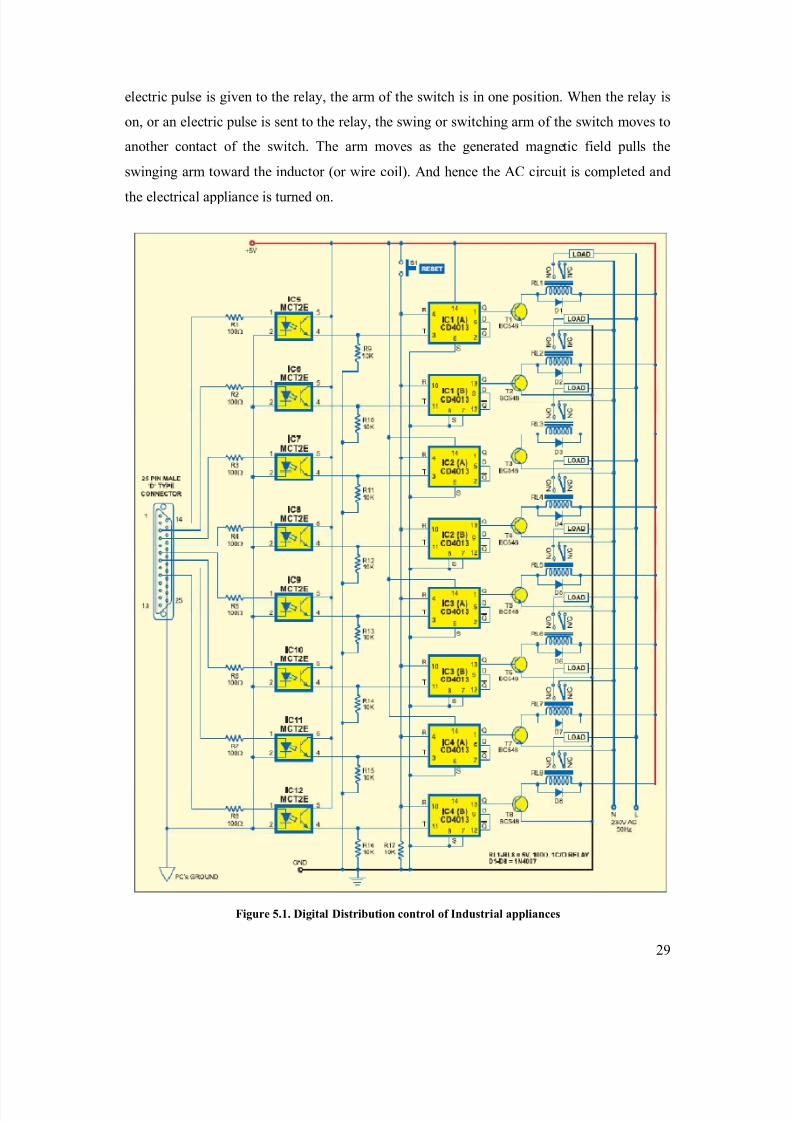
8/6/2019 Nikhil Project Report(Viii Sem)
http://slidepdf.com/reader/full/nikhil-project-reportviii-sem 29/46
29
electr ic pu lse is given to the re lay, the arm of the sw itch is in one pos ition. When the re lay is
on, or an e lectr ic pu lse is sen t to the re lay, the sw ing or sw itching arm of the sw itch mo ves to
ano ther con tact of the sw itch. The arm mo ves as the genera ted ma gnetic f ield pu lls the
swinging arm toward the induc tor (or w ire co il). And hence the AC c ircu it is comp leted and
the e lectr ica l appliance is turned on.
Figure 5.1. D igita l Distr ibut ion contro l of Industr ia l app liances

8/6/2019 Nikhil Project Report(Viii Sem)
http://slidepdf.com/reader/full/nikhil-project-reportviii-sem 30/46
30
F igure 5.2. Power supp ly c ircu it
F igure 5.3. Screenshot of the ma in screen for computer iz ed e lectr ica l equ ipment contro l
Howe ver, Trans istors and ICs mus t be pro tected from the br ief h igh voltage produced
when a re lay co il is sw itched off. The pro tection d iode a llows the induced voltage to dr ive a
br ief curren t throu gh the co il (and d iode) so the ma gnetic f ield d ies away qu ick ly ra ther than
instan tly. Th is prevents the induced voltage becom ing high enou gh to cause dama ge to
trans istors and ICs.
5.2.1. Background
Para llel por t is a s imple and inexpens ive tool for bu ilding compu ter con trolled de vices
and projec ts. The s implicity and ease of pro gramm ing makes para llel por t popu lar inelectron ics hobby ist wor ld. The para llel por t is of ten used in compu ter con trolled robo ts,
home au toma tion, e tc. Here is a s imple tutor ial on para llel por t interfac ing and pro gramm ing,
with some examp les. The pr imary use of para llel por t is to connec t pr inters to the compu ter
and is spec if ica lly des igned for this purpose.
8/6/2019 Nikhil Project Report(Viii Sem)
http://slidepdf.com/reader/full/nikhil-project-reportviii-sem 31/46
31
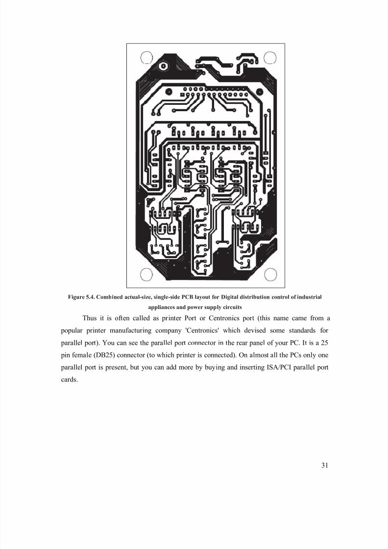
F igure 5.4. Comb ined actua l-s ize, s ing le-s ide PC B layout for D igita l d istr ibut ion contro l of industr ial
app liances and power supp ly c ircu its
Thus it is of ten ca lled as pr inter Por t or Cen tron ics por t (this name came from a
popu lar pr inter manufac tur ing company 'Cen tron ics' wh ich de vised some s tandards for
para llel por t). You can see the para llel por t connec tor in the rear pane l of your PC. I t is a 25
pin fema le (DB25) connec tor ( to wh ich pr inter is connec ted). On a lmost all the PCs on ly one
para llel por t is presen t, but you can add more by buy ing and inser ting ISA /PCI para llel por t
cards.
8/6/2019 Nikhil Project Report(Viii Sem)
http://slidepdf.com/reader/full/nikhil-project-reportviii-sem 32/46
32
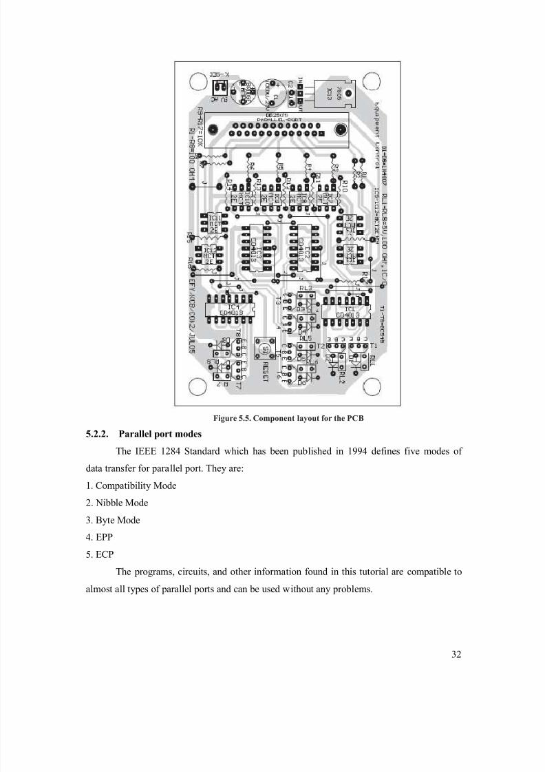
Figure 5.5. Component layout for the PC B
5.2.2. Para llel port modes
The IEEE 12 84 Standard wh ich has been pub lished in 199 4 def ines f ive modes of
data transfer for para llel por t. They are:
1. Compa ti bilit y Mode
2. N i bble Mode
3. By te Mode
4. EPP5. ECP
The pro grams, c ircu its, and o ther informa tion found in this tutor ial are compa ti ble to
almos t all types of para llel por ts and can be used w ithout any prob lems.
8/6/2019 Nikhil Project Report(Viii Sem)
http://slidepdf.com/reader/full/nikhil-project-reportviii-sem 33/46
33
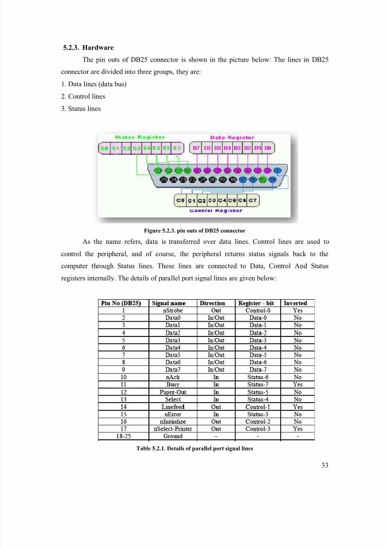
5.2.3. Hardware
The p in ou ts of DB25 connec tor is shown in the p icture be low: The lines in DB25
connec tor are d ivi ded into three groups, they are:
1. Da ta lines (da ta bus)
2. Con trol lines3. S tatus lines
Figure 5.2.3. p in outs of D B25 connector
As the name refers, da ta is transferred o ver da ta lines. Con trol lines are used to
control the per i phera l, and of course, the per i phera l returns s tatus s igna ls back to the
compu ter throu gh Status lines. These lines are connec ted to Da ta, Con trol And S tatus
registers interna lly. The de tails of para llel por t signa l lines are given be low:
T ab le 5.2.1. Deta ils of para llel port s igna l lines

8/6/2019 Nikhil Project Report(Viii Sem)
http://slidepdf.com/reader/full/nikhil-project-reportviii-sem 34/46
34
5.2.4. Para llel port reg isters
As you know, the Da ta, Con trol and S tatus lines are connec ted to there correspond ing
registers inside the compu ter. So, by man i pulating these re gisters in pro gram, one can eas ily
read or wr ite to para llel por t with pro gramm ing languages like 'C' and BASIC. The re gisters
found in a s tandard para llel por t are:
1. Da ta re gister
2. S tatus re gister
3. Con trol register
As their names spec ify, Da ta register is connec ted to Da ta lines, Con trol register is
connec ted to Con trol lines and S tatus re gister is connec ted to S tatus lines. (Here the word
connec tion does no t mean that there is some phys ical connec tion be tween da ta/control/status
lines. The re gisters are vir tually connec ted to the correspond ing lines.) So, wha tever you
wr ite to these re gisters w ill appear in the correspond ing lines as voltages. Of course, you can
measure it with a mu ltimeter. And wha tever you give to Para llel por t as voltages can be read
from these re gisters (w ith some res tr ictions). For examp le, if we wr ite '1' to Da ta re gister, the
line Da ta0 w ill be dr iven to +5 v. Jus t like this, we can pro gramma tically turn on and off any
of the Da ta lines and Con trol lines.
5.2.5. L IS T OF COMPON E NTS US E D:
1. 25 p in connec tor (DB25 ma le) and DB25 cab le.
2. Two 470ohm res istors.
3. 4n35 op tocoup ler.
4. 4.7K ohm res istor.
5. 2N2222 /BC148 .
6. Re lay 6v/100ohm.
7. 1N 4001D iode.
8. 6v battery.
9. One 3 pin p lug and socke t.
10. One LED.
11. Connec ting wires.
12. 2 30 v A.C. ma in supp ly.
13. Pr inted C ircu it Board.
5.2. 6 . App licat ions:
The projec t can be used for var ious app lications where ver you requ ire con trol using pc.

8/6/2019 Nikhil Project Report(Viii Sem)
http://slidepdf.com/reader/full/nikhil-project-reportviii-sem 35/46
35
a) Ho tel power mana gemen t.
b) S treet light mana gemen t.
c) Home au toma tion.
d) H igh voltage gr id con trol.
e) Indus tr ial au tomation and many more.
8/6/2019 Nikhil Project Report(Viii Sem)
http://slidepdf.com/reader/full/nikhil-project-reportviii-sem 36/46
36
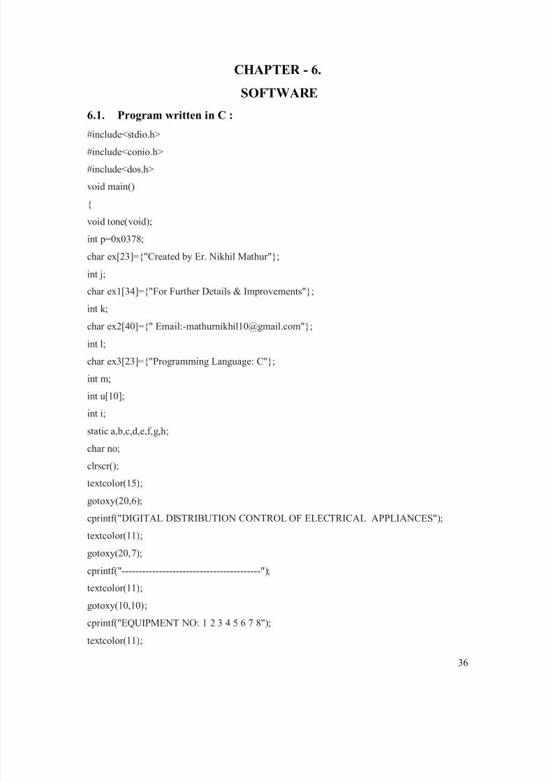
CHAP TE R - 6 .
SOF T WAR E 6 .1. Program wr itten in C :
#include<s tdio.h>#include<con io.h>
#include<dos.h>
void ma in()
{
void tone( void);
int p=0x0 378 ;
char ex[2 3]={"Crea ted by Er. N ikhil Mathur"} ;
int j; char ex1[ 34] ={"For Fur ther De tails & Impro vemen ts"} ;
int k ;
char ex2[ 40]={" Ema il:-ma thurn [email protected]"} ;
int l;
char ex 3[23]={"Pro gramm ing Language: C"} ;
int m;
int u[10 ];
int i;
static a,b,c,d,e,f, g,h;
char no ;
clrscr() ;
textcolor(15) ;
gotoxy(20,6) ;
cpr intf("DIGITAL DISTRIBUTION CONTROL OF ELECTRICAL APPLIANCES") ;
textcolor(11) ;
gotoxy(20, 7);
cpr intf("-----------------------------------------") ;
textcolor(11) ;
gotoxy(10,10) ;
cpr intf("EQUIPMENT NO: 1 2 3 4 5 6 7 8");
textcolor(11) ;

8/6/2019 Nikhil Project Report(Viii Sem)
http://slidepdf.com/reader/full/nikhil-project-reportviii-sem 37/46
37
gotoxy(10,12) ;
cpr intf("STATUS: %d %d %d %d %d %d%d %d",a,b,c,d,e,f, g,h) ;
textcolor(10) ;
gotoxy(9,16) ;
cpr intf("FOR 'ON' AND 'OFF' AN EQUIPMENT PRESS CORRESPONDING EQUIP. NO.") ;
textcolor(11) ;
gotoxy(2 8,18);
cpr intf("STATUS 0=OFF STATUS 1=ON") ;
textcolor(12) ;
gotoxy( 32,20) ;
cpr intf("FOR EXIT PRESS 'E'\n") ;
no=getch() ;
switch(no)
{
case '1':
a=!a ;
tone() ;
out por t b(p,1) ;
delay(500) ;
out por t b(p,0) ;
break ;
case '2':
b=!b ;
tone() ;
out por t b(p,2) ;
delay(500) ;
out por t b(p,0) ;
break ;
case ' 3 ':
c=!c ;
tone() ;
out por t b(p, 4);
delay(500) ;

8/6/2019 Nikhil Project Report(Viii Sem)
http://slidepdf.com/reader/full/nikhil-project-reportviii-sem 38/46
38
out por t b(p,0) ;
break ;
case ' 4 ':
d=!d ;
tone() ; out por t b(p, 8);
delay(500) ;
out por t b(p,0) ;
break ;
case '5':
e=!e ;
tone() ;
out por t b(p,16) ;
delay(500) ;
out por t b(p,0) ;
break ;
case '6':
f=!f ;
tone() ;
out por t b(p, 32);
delay(500) ;
out por t b(p,0) ;
break ;
case ' 7 ':
g=!g;
tone() ;
out por t b(p,6 4);
delay(500) ;
out por t b(p,0) ;
break ;
case ' 8 ':
h=!h ;
tone() ;
out por t b(p,12 8);

8/6/2019 Nikhil Project Report(Viii Sem)
http://slidepdf.com/reader/full/nikhil-project-reportviii-sem 39/46
39
delay(500) ;
out por t b(p,0) ;
break ;
case 'e':
if((a|b|c|d|e|f| g|h)==1){
clrscr() ;
textcolor(10) ;gotoxy(20,12) ;
cpr intf("PLEASE SHUT DOWN ALL THE EQUIPMENTS") ;
sound(200) ;
delay(500) ;
nosound() ;
delay(3000) ;
break ;
}
else
{
clrscr() ;
for(j=0 ; j<23; j++)
{
textcolor(10) ;gotoxy(20+j,12) ;
cpr intf("%c",ex[j ]);
sound( 3000+j) ;
delay(30);
nosound() ;
}
for(m=0 ;m<23;m++)
{
textcolor(10) ;gotoxy(20+m,1 3);
cpr intf("%c",ex 3[m]);
sound(1 800+m) ;
delay(30);
nosound() ;
}

8/6/2019 Nikhil Project Report(Viii Sem)
http://slidepdf.com/reader/full/nikhil-project-reportviii-sem 40/46
40
for(k=0 ;k<34 ;k++)
{
textcolor(10) ;gotoxy(20+k,1 4);
cpr intf("%c",ex1[k ]);
sound(2000+k) ; delay(30);
nosound() ;
}
for( l=0;l<40;l++)
{
textcolor(10) ;gotoxy(20+ l,15) ;
cpr intf("%c",ex2[ l]);
sound(2500+ l);
delay(30);
nosound() ;
}
pr intf("\n\n\n\nPress any key") ;
getch() ;
out por t b(p,0) ;exit(0);
}
case 'E':
if((a|b|c|d|e|f| g|h)==1)
{
clrscr() ;
textcolor(10) ;gotoxy(20,12) ;
cpr intf("PLEASE SHUT DOWN ALL THE EQUIPMENTS") ;
sound(200) ;
delay(500) ;
nosound() ;
delay(3000) ;
break ;
}
else
{

8/6/2019 Nikhil Project Report(Viii Sem)
http://slidepdf.com/reader/full/nikhil-project-reportviii-sem 41/46
41
clrscr() ;
for(j=0 ; j<23; j++)
{
textcolor(10) ;gotoxy(20+j,12) ;
cpr intf("%c",ex[j ]); sound(2500+j) ;
delay(30);
nosound() ;
}
for(m=0 ;m<23;m++)
{
textcolor(10) ;gotoxy(20+m,1 3);
cpr intf("%c",ex 3[m]);
sound( 3500+m) ;
delay(30);
nosound() ;
}
for(k=0 ;k<34 ;k++)
{
textcolor(10) ;gotoxy(20+k,1 4);
cpr intf("%c",ex1[k ]);
sound( 3000+k) ;
delay(30);
nosound() ;
}
for( l=0;l<40;l++)
{
textcolor(10) ;gotoxy(20+ l,15) ;
cpr intf("%c",ex2[ l]);
sound( 3500+ l);
delay(30);
nosound() ;
}
pr intf("\n\n\n\nPress any key") ;

8/6/2019 Nikhil Project Report(Viii Sem)
http://slidepdf.com/reader/full/nikhil-project-reportviii-sem 42/46
42
getch() ;
out por t b(p,0) ;exit(0);
}
defau lt:
clrscr() ; sound(500) ;
delay(100) ;
nosound() ;
textcolor(11) ;gotoxy( 30,12) ;
cpr intf("INVALID K EY PRESSED") ;
textcolor(11) ;gotoxy( 33 ,14);
cpr intf("WAIT 2 SECONDS") ;
delay(3000) ;
break ;
}
main();
}
void tone( void)
{
sound(1000) ;
delay(100) ;
nosound() ;
}
8/6/2019 Nikhil Project Report(Viii Sem)
http://slidepdf.com/reader/full/nikhil-project-reportviii-sem 43/46
43
CHAP TE R - 7
CONC LUSION
7.1. Conc lus ion
The conc lusion of the projec t is that whene ver the voltage or a d igital signa l µ1¶ isapplied on the para llel por t of the compu ter us ing the sof tware wh ich is wr itten in ³c´ then
the voltage on the correspond ing pin dr ives the op tocoup ler. When the voltage is app lied,
then the op tocoup ler ac tivates the trans istor inside the op tocoup ler wh ich dr ives the trans istor
BC 1 48 . The trans ition in the res istance of the c ircu it due to var iation in voltages across the
optocoup ler makes the trans istor BC 1 48 ON. The trans istor in turn ener gizes the co il in the
relay .The ener gized co il makes connec tion be tween the two term ina ls of the o ther c ircu it in
which the e lectr ical app liance is connec ted. And hence the AC c ircu it is comp leted. Ano ther
very interes ting conc lusion of this projec t is use of the re lay whose connec tion is to be madevery carefu lly otherw ise the c ircu it will not work. Precau tions mus t be taken under e very s tep
of so lder ing the c ircu it.
With the know ledge of new techn iques in µElectron ics¶ we are ab le to make our life
more comfor tab le. One such app lication of e lectron ics is used in ³PC CONTROLLED FAN
REGULATOR´.
The same c ircu it f inds its use in many more app lications. By this the intens ity of light
can be con trolled us ing a PC. The intens ity of light can be con trolled in f ive levels from off
pos ition to max imum intens ity poss i ble. So it f inds use as a n ight lamp by keep ing the
intens ity of lamp in low level.
The c ircu it also f inds its use for sw itching ON and OFF any e lectron ic c ircu itry. Our
norma l T.V PC can be used for a ll these purposes. So it is very usefu l or a rea l hel p to o ld age
and s ick peop le, since they can con trol the speed from the p lace where they are s itting.
We fee l that our produc t ser ves some thing good to this wor ld and we like to presen t it
before this prosperous wor ld.
7.2. Advantages y This circu it is s imple to use and eff icient.
y It can be assemb led w ith ease.
y It is cheap and hence very econom ic.
y It is sma ll in size.

8/6/2019 Nikhil Project Report(Viii Sem)
http://slidepdf.com/reader/full/nikhil-project-reportviii-sem 44/46
44
7.3. Scope of the project
The projec t hel ps in unders tand ing the work ing of the 25 p in para llel por t of the
compu ter, SPDT Re lay and Op tocoup ler. The scope of this projec t is hu ge w ith the
modern ization and ad vancemen t in compu ter f ields.
The projec t can be used for var ious app lications where ver you requ ire con trol using
pc.
a) Ho tel power mana gemen t.
b) S treet light mana gemen t.
c) Home au toma tion.
d) H igh voltage gr id con trol.
e) Indus tr ial au tomation and many more.
8/6/2019 Nikhil Project Report(Viii Sem)
http://slidepdf.com/reader/full/nikhil-project-reportviii-sem 45/46
45
CHAP TE R - 8
BIBL IOGRAPHY
8. R E F E R E NC E
y www.e lectron icsforyou.com
y www.hows tuffworks.com
y www.w ik i ped ia.or g
y Electron ics for You Ma gazine
y Electron ic Devices and C ircuits ± J. B.Gup ta
y Linear In tegrated c ircu its ± Gaykwad

8/6/2019 Nikhil Project Report(Viii Sem)
http://slidepdf.com/reader/full/nikhil-project-reportviii-sem 46/46
Cost Sheet


![B.Pharmacy [CBCS] Sem-I to SEm-VIII](https://img.dokumen.tips/doc/110x75/586cebc41a28ab84588ba0c8/bpharmacy-cbcs-sem-i-to-sem-viii.jpg)