Embed Size (px)
Citation preview
Journal of Engineering Science and Technology Vol. 12, No. 1 (2017) 113 - 126 © School of Engineering, Taylor’s University
113
NEW ELECTRONICALLY TUNABLE GROUNDED INDUCTOR SIMULATOR EMPLOYING SINGLE VDTA
AND ONE GROUNDED CAPACITOR
MAYANK SRIVASTAVA1, DINESH PRASAD
2,*, D. R. BHASKAR
3
1Department of Electronics and Communication Engineering, ASET, Amity University,
Sector-125, Noida (U.P.)-201313, India 2,3Department of Electronics and Communication Engineering, Faculty of Engineering and
Technology, Jamia Millia Islamia, New Delhi-110025, India
*Corresponding Author: [email protected]
Abstract
In this paper a new grounded inductor simulator employing single voltage
differencing transconductance amplifier (VDTA) and one grounded capacitor
has been proposed. The proposed circuit is electronically controllable and
exhibits low parasitic effects. The performance of proposed inductor simulator
is demonstrated by SPICE simulations with TSMC CMOS .18 µm process
parameters.
Keywords: Grounded inductor simulator, Electronic control, VDTA, Grounded
capacitor, Active inductor.
1. Introduction
The Inductor is an integral part of many analog circuits such as filters, oscillators,
phase shifters etc. A conventional spiral inductor has several drawbacks such as
large size and weight, generates unwanted harmonics of the signals due to
saturation of its core, picks as well as radiates electromagnetic waves etc. Its
quality factor and liner dimensions are directly proportional to each other. Hence,
it is not possible to design a small size inductor with high quality factor.
Therefore, in last three decades, attention is extensively focused on active
simulation of inductors. Numerous actively simulated grounded inductor
configurations employing different active building blocks such as operational
amplifiers (Op-amp)[1-4], current conveyors (CC) [5], Op-amps[6], voltage
current conveyors(DVCC)[7], CC[8], Op-amp[9], CCs [10-16], Current feedback-

114 M. Srivastava et al.
Journal of Engineering Science and Technology January 2017, Vol. 12(1)
Nomenclatures
CA, C’ Equivalent capacitances, μF
C0 , C1,
C2
External capacitances, μF
CP Parasitics capacitance at “P” port of VDTA, pF
CN Parasitics capacitance at “N” port of VDTA, pF
CX+ Parasitics capacitance at “X+” port of VDTA, pF
CX- Parasitics capacitance at “X-” port of VDTA, pF
CZ Parasitics capacitance at “Z” port of VDTA, pF
gm1, gm2,
gm
Transconductance gains of VDTA, μA/V
Ib1, Ib2,
Ib3, Ib4, Ib
Bias currents of VDTA, μA
IX+ Current at “X+” port of VDTA, mA
IX- Current at “X-” port of VDTA, mA
IZ Current at “Z” port of VDTA, mA
L, LA,
LGI, Leq
Equivalent inductances, μH
R1 External resistance, kΩ
R, RA,
R’, R
”
Equivalent resistances, kΩ
RP Parasitics resistance at “P” port of VDTA, kΩ
RN Parasitics resistance at “N” port of VDTA, kΩ
RX+ Parasitics resistance at “X+” port of VDTA, kΩ
RX- Parasitics resistance at “X-” port of VDTA, kΩ
RZ Parasitics resistance at “Z” port of VDTA, kΩ
s Laplace operator
Vin(s) Input voltage, V
Vout(s) Output voltage, V
VN Voltage port “N’ of VDTA
VP Voltage port “P” of VDTA
VVN Voltage at “N” port of VDTA, V
VVP Voltage at “P” port of VDTA, V
VZ Voltage at “Z” port of VDTA, V
W/L Shape factor
Zin Input impedance
Greek Symbols
βx+ Output stage tracking error (at por X+) of VDTA
βx- Output stage tracking error (at port X-) of VDTA
βz Input stage tracking error (at port Z) of VDTA
ω1, ω2 Pole frequencies, MHz
τ1, τ2 Time delays, μs
Abbreviations
CC Current conveyors
CDTA Current differencing transconductance amplifier
CFOA Current feedback operational amplifiers
CMOS Complementary metal oxide semiconductor

New Electronically Tunable Grounded Inductor Simulator Employing . . . . 115
Journal of Engineering Science and Technology January 2017, Vol. 12(1)
DC Direct current
DVCC Differential voltage current conveyors
FTFN Four terminal floating nullors
MOS Metal oxide semiconductor
OP-
AMP
Operational amplifiers
OTA Operational transconductance amplifier
OTRA Operational trans-resistance amplifier
SPICE Simulation Program with Integrated Circuit Emphasis
TSMC Taiwan Semiconductor Manufacturing Company
VDTA Voltage differencing transconductance amplifier
operational amplifiers (CFOA)[17-19], current differencing trans-conductance
amplifiers (CDTA)[20], four terminal floating nullors(FTFN)[21], Current Follower
transconductance amplifier (CFTA)[22], Fully Differential Second-Generation
Current Conveyor (FDCCII) )[23], Voltage differencing differential input buffered
amplifiers(VDDIBA)[24]. Dual output Differential Difference current conveyor
(DO-DDCC)[25], CFOA[26], Dual-X current conveyor (DX-CCII)[27-28],
Operational trans-conductance amplifiers(OTA)[29], Differential difference current
conveyor(DDCC)[30],operational trans-resistance amplifiers(OTRA)[31], voltage
differencing transconductance amplifiers (VDTA)[32], Voltage differencing
buffered amplifiers(VDBA) )[33] and Voltage differencing current
conveyors(VDCC)[34] have been proposed in the literature. Unfortunately, all of
the reported circuits suffer from one or more of following drawbacks:
(i) Excessive (more than one) use of the active components [1], [6], [7], [9],
[12], [14-16], [18], [20], [22], [24], [31].
(ii) Excessive(more than one) use of the passive components [1-3], [5], [6], [8-
11], [13], [15], [17-19], [21-23], [25-31], [33-34].
(iii) Partial utilization of active component(s) [7], [9], [18], [23], [29], [32-34].
(iv) Use of floating passive component(s) [1-11], [13], [15-19], [21], [25-31], [33].
(v) Lack of electronic controllability [1-6], [8-11], [13-19], [21], [23], [25-31].
(vi) Requirement(s) of external passive component matching constraints [1-3],
[8], [10-11], [13], [21], [27], [30-31].
(vii) High parasitic effects [24], [32-33].
Therefore, the purpose of this communication is to propose a new grounded
inductor simulator circuit composed of minimum active and passive components
(single VDTA and one grounded capacitor) with following advantageous features:
(i) use of a grounded capacitor, (ii) availability of electronic control, (iii) no
requirement of any external passive component matching constraint (iv) full
utilization of VDTA and (v) low parasitic effects.
2. Proposed Grounded Inductor Simulator
VDTA [35-36] is a versatile active element finds several applications in analog
filter designing [37-39], oscillators [40] and inductor simulators [41]. The
schematic symbol of the VDTA and CMOS implementation of VDTA are shown
in Fig. 1 and Fig.2 respectively, where P and N are input terminals and Z, X+ and

116 M. Srivastava et al.
Journal of Engineering Science and Technology January 2017, Vol. 12(1)
X- are output terminals. All terminals of VDTA exhibit high input impedance
values. The terminal characteristics of VDTA can be described by:
Z
V
V
m
m
mm
X
X
Z
V
V
V
g
g
gg
I
I
I
N
P
2
2
11
00
00
0 (1)
Fig. 1. The schematic symbol of VDTA.
Fig. 2. CMOS implementation of VDTA [36].
The proposed grounded inductance circuit is shown in Fig. 3. A routine
analysis of this circuit yields the following expression for its input impedance:
2
0
m
ing
sCZ (2)
with mmm ggg
21
Thus the circuit simulates a lossless grounded inductor with inductance value.
2
0
m
eqg
CL (3)
which is electronically tunable by gm .

New Electronically Tunable Grounded Inductor Simulator Employing . . . . 117
Journal of Engineering Science and Technology January 2017, Vol. 12(1)
The condition mmm ggg
21
can be easily achieved in practice by equating
the two bias currents of VDTA and does not require any external passive
component matching.
Fig. 3. Proposed grounded inductance simulator configuration.
3. Non-ideal analysis and effects of Parasitics
In the non ideal case, the VDTA can be characterized by the following equations
NPmZZ VVgI 1
(4)
ZmXX VgI2 (5)
ZmXX VgI2 (6)
where βZ, βX+ and βX- are voltage tracking errors.
Under non ideal conditions the input impedance of circuit proposed in figure 3
is given by
xzm
xzmin
g
sCgZ
2
0 (7)
Therefore, the circuit simulates a grounded series R - L circuit rather than a
pure grounded inductor at low frequencies.
where
xzm
xz
gR
(8)
and
xzmg
CL
2
0 (9)
To evaluate the high frequency performance, the proposed grounded inductor
is investigated under the influence of VDTA. X+ port parasitic impedance
consisting of a capacitor Cx+ in parallel with resistance Rx+, X- port parasitic
118 M. Srivastava et al.
Journal of Engineering Science and Technology January 2017, Vol. 12(1)
impedance consisting of a capacitor Cx- in parallel with resistance Rx-, P port
parasitic impedance consisting of a capacitor CP in parallel with resistance RP, N
port parasitic impedance consisting of a capacitor CN in parallel with resistance
RN and Z port parasitic impedance consisting of a capacitor CZ in parallel with
resistance RZ The expression of non ideal input impedance of proposed
configuration is found to be;
XP
X
XNZ
XZ
m
XNZ
XZ
in
sCsCR
sCsCsCsCRR
g
sCsCsCsCRR
Z111
11
0
2
0
(10)
where mmm ggg
21.
The non ideal equivalent circuit of proposed grounded inductor simulator
shown in Fig. 3 is given in Fig. 4.
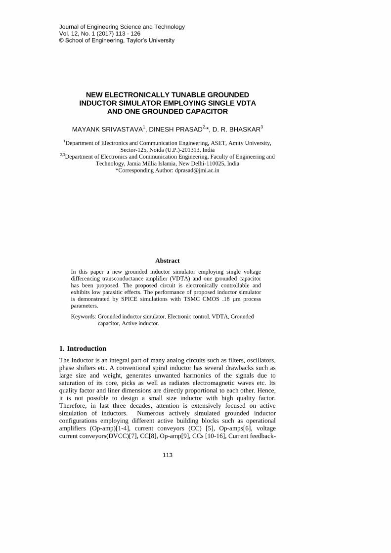
Fig. 4. Non ideal equivalent circuit of proposed grounded inductor simulator.
where
2
11
m
XZ
Ag
RRR
(11)
2
0 )(
m
NZ
Ag
CCCL
(12)
XPA CCC (13)
The grounded inductor simulator proposed in [32] as shown in Fig. 5, also
employs single VDTA and one grounded capacitor.
Fig. 5. Grounded inductor simulator proposed in [32].

New Electronically Tunable Grounded Inductor Simulator Employing . . . . 119
Journal of Engineering Science and Technology January 2017, Vol. 12(1)
The non non ideal equivalent circuit of grounded inductor simulator proposed
in [32] is shown in Fig. 6.
Fig. 6. Non ideal equivalent circuit of
grounded inductor simulator proposed in [32].
where
)1(
)(
21 zxmm
zxxGI
RRgg
RRCCL
(14)
zzxx
zxx
CRCCR
RRCCR
)(
)(' (15)
z
zzxx
R
RCRCCC
)(' (16)
)1(21
"
zxmm
z
RRgg
RR
(17)
zxx RRCCD )( (18)
On comparison of Fig. 4 with Fig. 6, it is clear that the effects of parasitics in
the proposed circuit are lower as compared to the circuit given in [32]. Hence, the
proposed configuration exhibits reduced parasitic effects.
The proposed inductor can be seen as another version of inductor simulator
proposed in [29] from the viewpoint of two OTA realization of VDTA. Grounded
inductor simulator proposed in [29] employs two OTAs along with one grounded
capacitor. The input negative terminals of first stage OTA is grounded so full
utilization of OTA is not achieved as an OTA is intended to produce output
current for differential input voltage but here at input side only one voltage input
is available. Moreover, in both the OTAs only one input is utilized so this work
can be done with single input/single output transconductance elements which
need less number of MOS transistors for implementation in comparison to MOS
transistors required to implement circuit given in [29]. So, all the resources of
[29] are not utilized which shows the wastage of resources. In our circuit both the
input terminals of VDTA are utilized.
The transconductance gains of VDTA are frequency dependent parameter,
which decide the bandwidth limitation of VDTA. The transconductances gm1 and
gm2 of VDTA can be described by single pole model as follows

120 M. Srivastava et al.
Journal of Engineering Science and Technology January 2017, Vol. 12(1)
11
01
1 s
gsg
m
m
(19)
21
02
2 s
gsg
m
m
(20)
where gm10 and gm20 are the transconductance gains at zero frequency and
1
1
1
and
2
2
1
are pole frequencies. Here, τ1 and τ2 are delays
corresponding to pole frequencies ω1 and ω2 respectively.
The bandwidth of VDTA can be improved by inserting a compensation
resistor RA, one voltage buffer and MOS transistor pair M9 and M10 in VDTA
CMOS structure shown in Fig.2. The modified CMOS structure is shown in Fig.
7. Transconductance gain gm1 for this modified VDTA can be given as
Am
m
mRg
gg
1
1
1 1
,
(21)
From Eq. (21) it is clear that gm1 of modified VDTA can be changed by
resistance “RA”. We know that bandwidth of VDTA depends on gm1. Hence,
bandwidth can also be controlled by RA.
Fig. 7. Modified CMOS structure of VDTA.
4. Application example

New Electronically Tunable Grounded Inductor Simulator Employing . . . . 121
Journal of Engineering Science and Technology January 2017, Vol. 12(1)
To illustrate the application of proposed grounded inductor simulator it has been
employed in the realization of a second order band pass filter as shown in Fig. 8.
Fig. 8. Voltage mode second order band pass filter
realized by proposed grounded inductor simulator.
The voltage transfer function of filter shown in Fig. 8 is given by:
21
2
21
2
21
)1
(
)1
(
)(
)(
CC
g
CRss
CRs
sV
sV
min
out
(22)
5. Simulation Result
The performance of the proposed structure has been confirmed by SPICE simulations
with TSMC CMOS 0.18μm process parameters with ORCAD 16.3 PSPICE
Simulator. The shape factors (W/L) of MOS transistors is given in Table 1.
Table 1. Shape factors (W/L) of MOS transistors.
Transistor W/L(μm)
M1 3.6/.36
M2 3.6/.36
M3 16.64/.36
M4 16.64/.36
M5 3.6/.36
M6 3.6/.36
M7 16.64/.36
M8 16.64/.36
For Simulations have been performed using CMOS VDTA [36] with component
values: C0 = 0.01nF, gm1=gm2=gm = 636.3 μA/V and power supply ± 0.9V DC. The
magnitude response and the phase response of the proposed simulated inductor are
shown in Fig. 9 and Fig. 10. From Fig. 9 it is clear that the simulated magnitude
response of proposed inductor is same as the ideal magnitude response in the

122 M. Srivastava et al.
Journal of Engineering Science and Technology January 2017, Vol. 12(1)
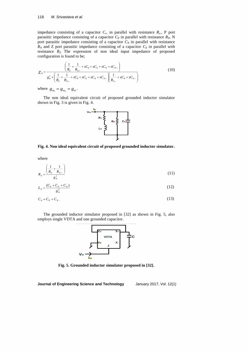
frequency range of 804 kHz to 31.62 MHz. similarly Figure 10 indicates that the ideal
and simulated phase responses are almost identical in frequency range of 5.012 MHz
to 31.42 MHz. the deviation of simulated responses from ideal responses at low
frequencies can be understood by Eq. (7), which shows that under the effects of non-
idealities, the proposed circuit works as a grounded series R-L circuit. The lossy term
“R” is responsible for the deviation of simulated responses from ideal responses. At
high frequencies the difference between ideal and simulated responses is mainly
due to the parasitics of VDTA terminals.
On comparing magnitude and phase response of our circuit and responses of
circuit given in [32] with ideal response, it is clear that at low frequencies the
responses of circuit given in [32] are a bit better due to non availability of lossy
term in non ideal conditions which is because of leaving “P” and “X-” terminal
unused in this circuit. The grounded “P” terminal results in wastage of recourses
and the parasitics of floating “X-” terminal are not balanced and will consume the
power. So, improved low frequency response of circuit proposed in [32] is at the
cost of wastage of recourses and power. At high frequencies the magnitude and
phase responses of circuit given in [32] is highly deviated from ideal response due
to presence of high parasitic effects. Our proposed circuit gives better response at
high frequency due to low parasitic effects. So, it is verified that proposed circuit
experience less parasitic effects in comparison to the circuit given in [32].
In proposed grounded inductor simulator, the bias currents Ib1= Ib2= Ib3= Ib4=
Ib for satisfying the condition gm1=gm2. The electronic control of proposed
configuration is demonstrated by changing Ib from 150 μA to 180 μA. Fig. 11
shows the magnitude responses of input impedance of proposed grounded
inductor at different bias currents Ib= 150 μA, 160 μA, 170 μA and 180 μA.
To confirm the workability of bandpass filter, the circuit was simulated using
the CMOS VDTA [36] with R1 = 1.58kΩ, C1 = 0.01nF, C2 = 5pF, gm1 =gm2 =gm=
636.3 μA /V with power supply ± 0.9V DC. The frequency response of this
realized bandpass filter is shown in Fig. 12, where central frequency of simulated
filter is found to be 14.1 MHz.
Fig. 9. Magnitude response.
105
106
107
108
101
102
103
104
105
Frequency(Hz)
Mag
nit
ud
e
Simulated (Ref 32)
Simulated (Proposed)
Ideal
New Electronically Tunable Grounded Inductor Simulator Employing . . . . 123
Journal of Engineering Science and Technology January 2017, Vol. 12(1)
Fig. 10. Phase response.
Fig. 11. Electronic tunability of magnitude
response of proposed grounded inductor simulator.
Fig. 12. Frequency response of second order voltage mode bandpass filter.
105
106
107
108
0
20
40
60
80
100
Frequency(Hz)
Ph
ase(d
eg
)
Simulated (Ref 32)
Simulated (Proposed)
Ideal
1 2 3 4 5 6 7 8 9 10
x 106
0
200
400
600
800
1000
1200
1400
1600
Frequency (Hz)
Ma
gn
itu
de
Ib= 150 uA
Ib= 160 uA
Ib= 170 uA
Ib= 180 uA

124 M. Srivastava et al.
Journal of Engineering Science and Technology January 2017, Vol. 12(1)
6. Conclusion
A new single VDTA based grounded inductor simulator circuit has been proposed
which offers electronic controllability and reduced parasitic effects. The proposed
configuration requires a realization condition which can be easily meet by equating
the two bias currents of VDTA. To verify the validity of the proposed grounded
inductor, a second order bandpass filter has been realized. The SPICE simulation
results confirm the theoretical predictions.
References
1. Ford, R.L.; and Girling, F.E.J. (1966). Active filters and oscillators using
simulated inductance. Electronics Letters, 2(2), 481-482.
2. Prescott, A.J. (1966). Loss compensated active gyrator using differential
input operational amplifier. Electronics Letters, 2(7), 283-284.
3. Orchard, H.J.; and Willson, A.N. (1974). New active gyrator circuits.
Electronics Letters, 10(13), 261-262.
4. Dutta Roy, S.C. (1975). On operational amplifier simulation of grounded
inductance. Archiv fuer Elektronik und Uebertragungstechnik, 29, 107-115.
5. Senani, R. (1978). Active simulation of inductors using current conveyors.
Electronics Letters, 14(15), 483-484.
6. Nandi, R. (1980). Novel insensitive lossless inductor simulation through
inverse function generation. Electronics Letters, 16(12), 481-482.
7. Nandi, R. (1980). Lossless inductor simulation: novel configurations using
DVCCS. Electronics Letters, 16(17), 666-667.
8. Paul, A.N.; and Patranabis, D. (1981) Active simulation of grounded
inductors using a single current conveyor. IEEE Transactions on Circuits and
Systems, 28(2), 164-165.
9. Fabre, A. (1992). Gyrator implementation from commercially available trans-
impedance operational amplifiers. Electronics Letters, 28(3), 263-264.
10. Arslan, E.; Cam, U.; and Cicekoglu, O. (2003). Novel lossless grounded
inductance simulators employing only a single first generation current
conveyor. Frequenz; Journal of RF Engineering and Telecommunications.
57(9-10), 204-206.
11. Yuce, E.; Minaei, S.; and Cicekoglu, O. (2005). A novel grounded inductor
realization using a minimum number of active and passive components. ETRI
Journal, 27(4), 427-432.
12. Parveen, T.; and Ahmed, M.T. (2006). Simulation of ideal grounded tunable
inductor and its application in high quality multifunctional filter.
Microelectronics International Journal, 23(3), 9-13.
13. Yuce, E.; Minaei, S.; and Cicekoglu, O. (2006). Limitations of the simulated
inductors based on a single current conveyor. IEEE Transactions on Circuits
and Systems, 53(12), 2860-2867.
14. Psychalinos, C.; and Spanidou, A. (2006). Current amplifier based grounded
and floating inductance simulators. International Journal of Electronics and
Communication (AEU), 60, 168-171.

New Electronically Tunable Grounded Inductor Simulator Employing . . . . 125
Journal of Engineering Science and Technology January 2017, Vol. 12(1)
15. Yuce, E. (2008). Grounded Inductor Simulators with Improved Low
Frequency Performances. IEEE Transactions on Instrumentation and
Measurement, 57(5), 1079-1084.
16. Pal, K.; and Nigam, M.J. (2008). Novel active impedances using current
conveyors. Journal of Active and Passive Electronic Devices, 3(1), 29-34.
17. Yuce, E.; and Minaei, S. (2008). A modified CFOA and its applications to
simulated inductors, capacitance multipliers, and analog filters. IEEE
Transactions on Circuits and Systems, 55(1), 254-263.
18. Yuce, E.; and Minaei, S. (2009). On the realization of simulated inductors
with reduced parasitic impedance effects. Circuits Systems and Signal
Processing, 28(3), 451 - 465.
19. Yuce, E. (2009). Novel lossless and lossy grounded inductor simulators
consisting of a canonical number of components. Analog Integrated Circuits
and Signal Processing, 59(1), 77-82.
20. Prasad, D.; Bhaskar, D.R.; and Singh, A.K. (2010). New grounded and
floating simulated inductance circuits using current differencing
transconductance amplifiers. Radioengineering, 19(1), 194- 198, 2010.
21. Kumar, P.; and Senani, R. (2010). New grounded simulated inductance
circuit using a single PFTFN. Analog Integrated Circuits and Signal
Processing, 62(1), 105-112.
22. Herencsar, N.; Koton, J.; and Vrbra, K. (2010). CFTA-based active-C
grounded positive inductance simulator and its application, Elektrorevue,
1(1) 24-27.
23. Kacar, F. (2010). New lossless inductance simulators realization using a
minimum active and passive components. Microelectronics Journal, 41(2-3),
109-113.
24. Prasad, D.; Bhaskar, D.R.; and Pushkar, K.L. (2011). Realization of new
electronically controllable grounded and floating simulated inductance
circuits using voltage differencing differential input buffered amplifiers.
Active and Passive Electronic Components, 2011, 8 pages.
25. Ibrahim, M.A.; Minaei, S.; Yuce, E.; Herencsar, N.; and Koton, J. (2011)
Lossless grounded inductance simulation using only one modified dual
output DDCC. Proceedings of the 34thInternational Conference on
Telecommunications and Signal Processing (TSP2011), Budapest, Hungary,
261-264.
26. Kacar, F.; and Kuntman, H. (2011). CFOA-based lossless and lossy
inductance simulators, Radioengineering, 20(3), 627-631.
27. Metin, B. (2011). Supplementary inductance simulator topologies employing
single DXCCII. Radioengineering, 20(3), 614 -618.
28. Myderrizi, I.; Minaei, S.; and Yuce, E. (2011). DXCCII based grounded
inductance simulators and filter applications. Microelectronics Journal,
42(9), 1074-1081.
29. Geiger, R.L.; and Sanchez-Sinencio, E. (1985). Active filter design using
operational transconductance amplifier: A tutorial. IEEE Circuits and
Devices Magazine, 1(2), 20-32.

126 M. Srivastava et al.
Journal of Engineering Science and Technology January 2017, Vol. 12(1)
30. Ibrahim, M.A.; Minaei, S.; Yuce, E.; Herencsar, N.; and Koton, J. (2012).
Lossy/lossless floating/grounded inductance simulator using one DDCC.
Radioengineering, 21(1), 2-10.
31. Gupta, A.; Senani, R.; Bhaskar, D.R.; and Singh, A.K. (2012). OTRA-based
grounded-FDNR and grounded-inductance simulators and their applications.
Circuits, Systems, and Signal Processing, 31(2), 489-499, 2012.
32. Prasad, D.; and Bhaskar, D.R. (2012). Grounded and floating inductance
simulation circuits using VDTAs. Circuits and Systems, 3(4), 342-347.
33. Yesil. A.; Kacar, F.; and Gurkan, K. (2014). Lossless grounded inductance
simulator employing single VDBA and its experimental band-pass filter
application. International Journal of Electronics and Communication (AEU),
68(2), 143-150.
34. Kacar. F.; Yesil, A.; Minaei, S.; and Kuntman, H. (2014). Positive/negative
lossy/lossless grounded inductance simulators employing single VDCC and
only two passive elements. International Journal of Electronics and
Communication (AEU), 68(1), 73-78.
35. Biolek, D.; Senani, R.; Biolkova, V.; and Kolka, Z. (2008). Active elements
for analog signal processing; classification, review and new proposals.
Radioengineering, 17(4), 15-32.
36. Yesil, A.; Kacar, F.; and Kuntman, H. (2011). New simple CMOS realization
of voltage differencing transconductance amplifier and its RF filter
application. Radioengineering, 20(3), 632-637.
37. Prasad, D.; Bhaskar, D.R.; and Srivastava, M. (2013). Universal Current-
Mode Biquad Filter using a VDTA. Circuits and Systems, 4(1), 32-36.
38. Prasad, D.; Bhaskar, D.R.; and Srivastava, M. (2013). Universal voltage-
mode biquad filter using voltage differencing transconductance amplifier.
Indian Journal of Pure and Applied Physics, 51(12), 864-868.
39. Prasad, D.; Srivastava, M.; Bhaskar, D.R. (2014). Transadmittance - Type
Universal Current-Mode Biquad Filter using Voltage Differencing
Transconductance Amplifiers. International Scholarly Research Network,
2014, 4 pages.
40. Prasad, D.; Srivastava, M.; Bhaskar, D.R. (2013). Electronically controllable
fully uncoupled explicit current mode quadrature oscillator using VDTA and
grounded capacitors. Circuits and Systems. 4(2), 169-172.
41. Srivastava, M.; Prasad, D.; Bhaskar, D.R. (2014). New Parallel R-L
impedance using single VDTA & its high pass filter applications. In
Proceedings of International Conference on Signal Processing and
Integrated Networks-2014(SPIN-2014),Noida, India, 535-537.