Embed Size (px)
Citation preview
Transient Analysis of an Electrostatically Tunable Multiferroic Inductor
A Thesis Presented
by
Carl Joseph Hansen
to
The Department of Electrical and Computer Engineering
in partial fulfillment of the requirements for the degree of
Master of Science
in
Electrical and Computer Engineering
Northeastern University Boston, Massachusetts
August 2013
ii
ABSTRACT
This thesis examines the dynamic behavior of an electric-field tunable
multiferroic inductor, a four-terminal device that is comprised of a two-terminal variable
inductor with an inductance controlled by a two-terminal voltage input. Although the
inductor features a wide tuning range and high quality factor, little information is
available regarding the inductor’s transient characteristics in response to a fast changing
control voltage. Therefore, its role in certain high-speed electronic applications is
currently undetermined.
To reduce the aforementioned knowledge gap, the time-varying tuning response
of the multiferroic tunable inductor is explored in this thesis to establish its relevance to
high-speed electronics. Specifically, it is demonstrated that the multiferroic tunable
inductor can achieve a newly selected inductance value within a settling time of ten
microseconds. To accomplish this, the following steps are performed: First, a
mathematical model is developed that provides insight into the tunable inductor’s
physical behavior. Next, techniques for achieving a high-speed tuning response are
studied, including the derivation of measurable parameters, design and analysis of proper
electronic driver circuits, and measurement and processing techniques. Finally, a
laboratory measurement setup is designed and constructed to test the tunable inductor and
prove the stated hypothesis.
Results show that electrostatically tunable multiferroic inductors are well suited
for high-speed applications, and that tuning speeds of several microseconds are
achievable with appropriate driver electronics. These results bode well for electric-field
tunable multiferroic inductors and their use in radio frequency applications.
iii
TABLE OF CONTENTS
LIST OF FIGURES v
LIST OF TABLES vii
1 INTRODUCTION 1
1.1 Motivation 2
1.1.1 Tunable Inductors 2
1.1.2 High-Performance Tunable Inductors 8
1.2 Objective 11
1.3 Outline 12
2 LITERATURE REVIEW 13
2.1 Background 13
2.2 Performance 16
2.2.1 Tuning Range 16
2.2.2 Quality Factor 18
2.2.3 Tuning Speed 19
2.3 Modeling 21
2.3.1 Piezoelectric 21
2.3.2 Ferromagnetic 26
2.3.3 Time-Varying Inductance 26
2.4 Actuation 27
3 METHODOLOGY 31
3.1 Electrostatically Tunable Multiferroic Inductor Dynamics 31
3.1.1 Linear Time-Invariant Inductor 32
3.1.2 Linear Time-Variant Inductor 34
3.1.3 Linear Time-Variant Inductor Simulation 47
3.1.4 Non-Linear Time-Variant Inductor 52
3.1.5 Non-Linear Time-Variant Inductor Simulation 61
3.1.6 Measurement Techniques Summary 62

iv
3.2 Actuator Electronics 63
3.2.1 Load Requirements 63
3.2.2 Custom Amplifier 65
3.2.3 COTS Amplifier 67
3.2.4 Amplifier Implementation 70
3.3 Laboratory Measurement System 73
4 RESULTS 78
4.1 Sinusoidal Method 80
4.2 Constant Current Method 83
5 DISCUSSION 87
5.1 Tuning Speed 87
5.2 Measurement Techniques 89
5.3 Future Work 92
6 CONCLUSION 94
7 REFERENCES 95
APPENDIX A 100

v
LIST OF FIGURES
Figure 1.1: Voltage-Controlled Oscillator 3
Figure 1.2: Tunable Voltage Controlled Oscillator 4
Figure 1.3: Second Order Band-Pass Filter 5
Figure 1.4: Tunable Filter Implemented with Only Tunable Capacitors 9
Figure 1.5: Voltage-Controlled Oscillator (RF MEMS Implementation) 10
Figure 2.1: Electrostatically Tunable Multiferroic Inductor 13
Figure 2.2: Multiferroic Inductor Inductance 17
Figure 2.3: Multiferroic Inductor Tunability 17
Figure 2.4: Multiferroic Inductor B-H Curve 18
Figure 2.5: Multiferroic Inductor Quality Factor 19
Figure 2.6: Butterworth Van Dyke Piezoelectric Circuit Model 22
Figure 2.7: Simulated PZT Impedance vs. Frequency (BVD Model) 23
Figure 2.8: Simulated Impedance Magnitude vs. Frequency 24
Figure 2.9: Simulated Impedance Phase vs. Frequency 24
Figure 2.10: Guan Piezoelectric Circuit Model with Mechanical Loading 25
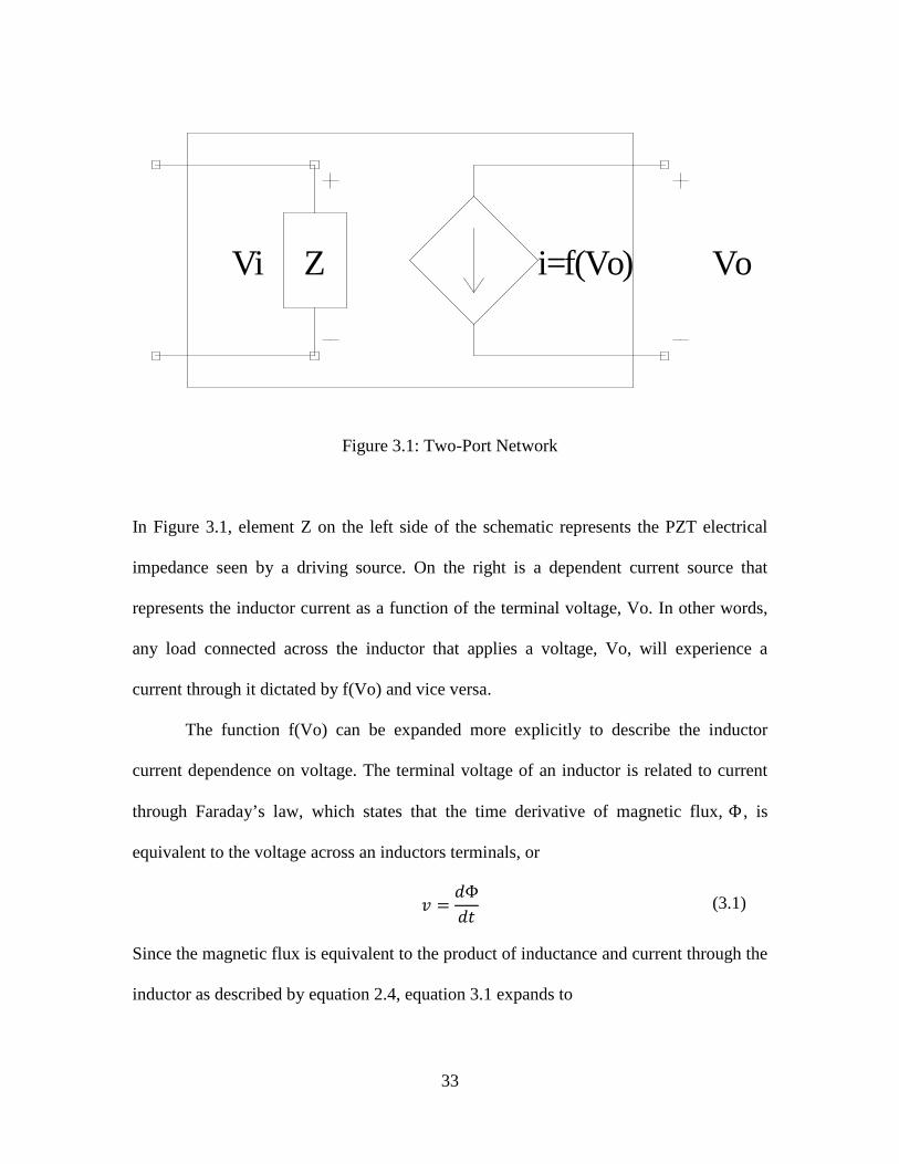
Figure 3.1: Two-Port Network 33
Figure 3.2: Modified Two-Port Network 35
Figure 3.3: P(s) Frequency Response 38
Figure 3.4: Simulated PZT Charge Step Response 39
Figure 3.5: M(s) Frequency Response 43
Figure 3.6: SPICE Circuit Model of a Linear Time-Variant Electrostatically
47
Tunable Multiferroic Inductor
Figure 3.7: Inductor Voltage Step Response 50
Figure 3.8: Inductor Voltage Step Response (Zoomed) 51
Figure 3.9: Inductance Step Response 52
Figure 3.10: Magnetic Flux vs. Current vs. Permeability 55
Figure 3.11: Magnetic Flux vs. Current vs. Permeability (2D) 56

vi
Figure 3.12: Static Inductance vs. Current vs. Permeability 57
Figure 3.13: Dynamic Inductance (Current) vs. Current vs. Permeability 58
Figure 3.14: Dynamic Inductance (Permeability) vs. Current vs. Permeability 59
Figure 3.15: SPICE Schematic with Constant Current Source 61
Figure 3.16: Magnetic Flux Response to Determine Tuning Speed 62
Figure 3.17: PZT Impedance Magnitude and Phase 64
Figure 3.18: Custom Amplifier Voltage Output 67
Figure 3.19: Apex Microtechnology MP111 Equivalent Schematic 69
Figure 3.20: Unassembled MP111 Amplifier and EV57 Evaluation Kit 71
Figure 3.21: Assembled MP111 Amplifier and EV57 Evaluation Kit 71
Figure 3.22: MP111 Implementation Schematic 72
Figure 3.23: MP111 SPICE Model Simulated Step Response 73
Figure 3.24: Laboratory Measurement System 1 74
Figure 3.25: Laboratory Measurement System 2 75
Figure 3.26: Measurement Circuit 76
Figure 4.1: PZT Sample 1 78
Figure 4.2: PZT Sample 2 79
Figure 4.3: Measured Inductor Voltage Step Response 80
Figure 4.4: Measured PZT Current Response 81
Figure 4.5: Measured Inductor Voltage Step Response (Reverse Polarity) 82
Figure 4.6: Measured PZT Current Response 83
Figure 4.7: Measured Inductor Voltage Step Response 84
Figure 4.8: Measured Inductor Voltage Step Response (Reverse Polarity) 85
Figure 4.9: Measured Inductor Voltage Step Response 86
Figure 4.10: Measured PZT Current Response 86
Figure 5.1: High-Level Control Block Diagram 93
Figure A.1: Custom Amplifier Design Schematic 101

vii
LIST OF TABLES
Table 2.1: Piezoelectric Driver Circuit Comparison 29
Table 3.1: Apex Microtechnology MP111 Amplifier Specifications 68

1
1 INTRODUCTION
Multiferroic materials and devices are a popular research area due to their
electrostatically tunable magnetic properties and potential application as voltage-
controlled filters, phase shifters, and inductors in radio frequency (RF) circuits [1].
Comprised of magnetoelastic and piezoelectric components, the multiferroic
heterostructure features a magnetoelectric (ME) coupling effect. The ME effect induces a
change in the magnetoelastic permeability through excitation of the piezoelectric
element. This change in permeability can lead to the alteration of external magnetic fields
in exchange for very little static energy dissipation, as the piezoelectric material is a high-
impedance device that requires only a constant electric field (voltage).
Development of the ME effect for tunable inductors has been driven by the
inefficient, bulky electromagnet tuning found in traditional tunable inductors [2], and
continued innovation has led to multiferroic materials exceeding the tunable range of
competing novel devices [3]. Although multiferroics have shown wider tuning frequency,
other RF MEMS devices possess desired tuning response time in the microsecond range
[4]. To ensure successful application in the RF domain, similar tuning speed must be
achieved.
In this study, the performance of the novel multiferroic tunable inductor is
researched to ascertain its performance in high-speed RF applications. Particularly, the
response time of the inductance change with respect to the control input is characterized
and a methodology for achieving repeatable high-speed operation is developed. By
establishing the inductors suitability in high-speed applications, scientists and engineers
can confidently integrate these low-power components into a range of devices.

2
Ultimately, the employment of efficient, high-performance tunable components will
provide benefits across the electronics spectrum.
1.1 Motivation
The inspiration for researching the transient response of a tunable inductor
originates from the general need for fast-performing tunable inductors in high-frequency
applications. Since present applications for tunable devices derive mainly from the RF
domain, the following discussion cites two specific RF applications to support the study
of tunable inductors in general and, more specifically, multiferroic tunable inductors and
their transient characteristics.
1.1.1 Tunable Inductors
Many wireless (RF) communications technologies require a passive tunable
component in the front-end to facilitate various operational states. One example is the
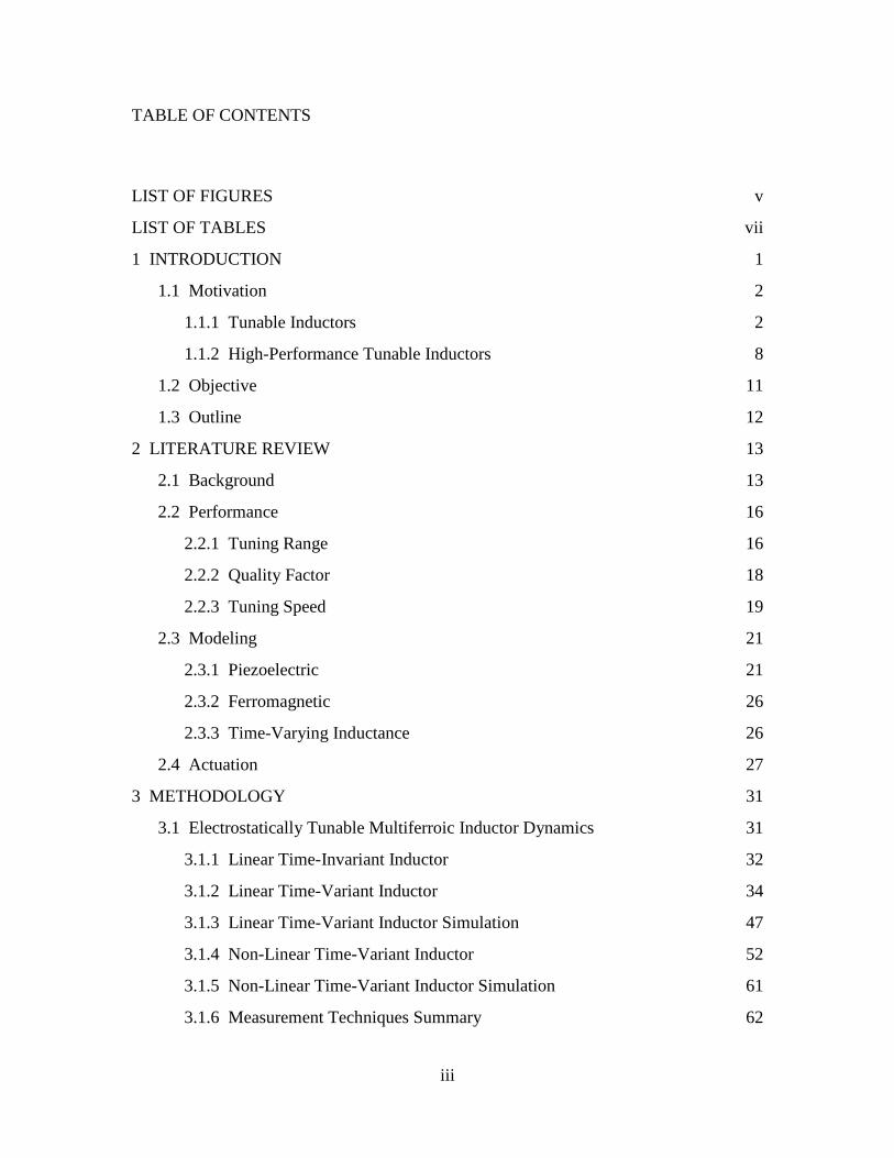
voltage-controlled oscillator (VCO), a device employed to generate the internal operating
frequencies essential to wireless transceivers. The VCO outputs a periodic signal whose
frequency is a function of the circuit topology. Figure 1.1 on the following page provides
an example schematic representation of the VCO [5].
In the example, the passive inductor (L) and passive capacitor (C) form a resonant
circuit alongside four active cross-coupled complementary metal oxide semiconductor
field-effect transistors (MOSFETs). Together, the components generate a particular
output frequency. Given the above topology in Figure 1, the output frequency is a direct
function of L and C, or:
3
𝑓0 = 𝑓(𝐿,𝐶) (1.1)
To achieve a fixed operating frequency, the VCO must employ static components
with values that do not drift over time. If either the inductor or capacitor is variable,
however, the output frequency will change as the component values change. Hence,
tunable components can directly tune the VCO frequency of operation to a desired value.
Figure 1.1: Voltage-Controlled Oscillator
M M
M M
C
L
VD
D
4
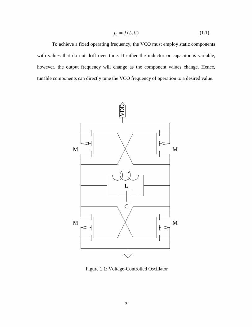
Figure 1.2: Tunable Voltage Controlled Oscillator
Given the option, designers may choose to implement a tunable inductor and a fixed
capacitor, a tunable capacitor and a fixed inductor, or a tunable inductor and tunable
capacitor as shown in Figure 1.2. The choice is typically dictated by performance,
availability, and/or component maturity. Since tunable capacitor research has yielded
many advancements in the tuning range of capacitors, these devices are easily
implemented as a VCO frequency-modifying component [5][6]. There are drawbacks to
solely using a capacitor, however, including increased device current consumption and
M M
M M
C
LV
DD
5
energy usage [5]. Thus, the inclusion of the tunable inductor as a complementary device
is often necessary and preferred to achieve the highest device performance. Examination
of another RF application, the tunable band-pass filter, further verifies the inductors
importance in tunable applications by illustrating an improved tunable range.
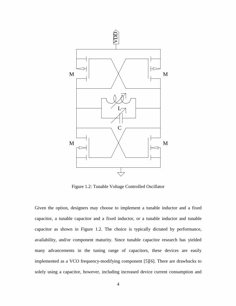
The tunable filter is required to selectively attenuate out-of-band signals
especially as reconfigurable RF front-end circuits are becoming increasingly popular for
multi-standard receivers [7]. Thus, a band-pass filter is useful in RF applications where
various carrier frequencies are received by an antenna, and a specific frequency is
required to be isolated for signal processing. Figure 1.3 demonstrates a second-order
resistor-inductor-capacitor (RLC) filter.
Figure 1.3: Second Order Band-Pass Filter
To illustrate the tunable inductors appeal, a nodal analysis is performed on the
circuit in Figure 1.3 to yield the following transfer function:
R
LCIN OUT

6
𝐻(𝑠) =𝑉𝑂𝑈𝑇(𝑠)𝑉𝐼𝑁(𝑠)
=𝑠 ∙ 𝑅𝐿
𝑠2 + 𝑠 ∙ 𝑅𝐿 + 1𝐿 ∙ 𝐶
(1.2)
For comparison, the general form of a second-order band-pass filter is as follows
[8]:
𝐻(𝑠) =𝑉𝑂𝑈𝑇(𝑠)𝑉𝐼𝑁(𝑠) =
𝑠 ∙ 𝜔0𝑄
𝑠2 + 𝑠 ∙ 𝜔0𝑄 + 𝜔0
2 (1.3)
Contrasting equations 1.2 and 1.3 demonstrates that the resonant frequency squared, or
𝜔02, is equivalent to the inverse of the product of inductance and capacitance in the filter,
or 1𝐿∙𝐶
. Also, the ratio of resonant (or center) frequency to quality factor, 𝜔0𝑄
, is equivalent
to the ratio of resistance to inductance, 𝑅𝐿. Both of these ratios help to define the filter
characteristics and both ratios include an inductive term, a clue to recognizing the value
of a tunable inductor.
The quality factor is an often used indicator of reactive efficiency. Specifically, 𝑄
relays the ratio of stored energy to dissipated energy per signal cycle. In a second-order
filter, the quality factor also signifies the bandwidth range, where low quality represents a
wide band of passable frequencies and high quality signifies a narrow band. In RF
applications, filters with a high quality factor are preferred as they support more
frequency selective processing.
Given 𝜔0 = � 1𝐿∙𝐶
and 𝜔0𝑄
= 𝑅𝐿, solving for 𝑄 yields
𝑄 =𝐿 ∙ 𝜔0
𝑅=
1𝑅∙ �
𝐿𝐶
(1.4)

7
Equation 1.4 suggests that a high quality factor can be achieved through manipulation of
the component values in three different ways:
1. Decrease resistance
2. Decrease capacitance
3. Increase inductance
Since resistance is inversely proportional to quality factor, the value of 𝑅 should
be as low as possible. Regarding the reactive components, inductance is proportional to
quality factor while capacitance is inversely proportional, or
𝐿 ∝ 𝑄 (1.5)
𝐶 ∝1𝑄
(1.6)
In other words, if a tunable inductor has its value increased while the capacitance
remains fixed, the quality factor will increase until the inductor reaches its maximum
tunable value. Similarly, if a tunable capacitor has its value reduced in equation 1.4 while
the inductor remains fixed, the quality factor will increase until the capacitor reaches its
maximum tunable value. Thus, if a designer can utilize a tunable inductor in addition to a
tunable capacitor, the quality factor may be extended beyond the range capable with only
a single tunable component.
The analysis presented above can also be applied to moving the resonant (center)
frequency for the selection of different bands. Since inductance and capacitance are
inversely proportional to resonant frequency, modification of both terms in the
inductance/capacitance product results in a greater tunable range than modification of a
single term.
8
𝐿 ∙ 𝐶 ∝1𝜔𝑜
(1.7)
Hence, designing a tunable filter with both a tunable inductor and a tunable
capacitor offers increased range versus a tunable filter without the complementary pair.
The concepts presented here also extend to the VCO and other tunable applications
requiring pairs of reactive components, ultimately suggesting that achieving high
performance in RF applications requires the inclusion of tunable inductors.
1.1.2 High-Performance Tunable Inductors
In the above examples, the tunable inductor was shown to achieve improved
circuit performance when paired with a complementary device. An arbitrary inductor,
however, is not suitable for all designs. In RF applications, designers must ensure that the
tunable inductor meets certain performance criteria related to high-frequency operation
before implementation in a particular circuit. These criteria include quality factor, tuning
range, and tuning speed. If the high-speed criteria are not met, alternative options that
sacrifice performance may be required. An example is a device comprised of only tunable
capacitors when no sufficient tunable inductor is available [9]. Therefore, researching the
performance of these inductor parameters and finding a balance between high tuning
range, quality factor, and tuning speed is critical to developing devices that include
tunable inductors and achieving maximum RF performance.
9
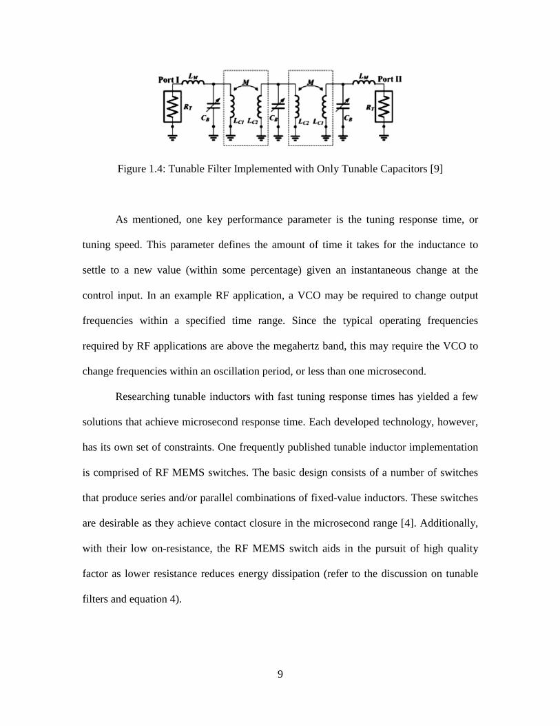
Figure 1.4: Tunable Filter Implemented with Only Tunable Capacitors [9]
As mentioned, one key performance parameter is the tuning response time, or
tuning speed. This parameter defines the amount of time it takes for the inductance to
settle to a new value (within some percentage) given an instantaneous change at the
control input. In an example RF application, a VCO may be required to change output
frequencies within a specified time range. Since the typical operating frequencies
required by RF applications are above the megahertz band, this may require the VCO to
change frequencies within an oscillation period, or less than one microsecond.
Researching tunable inductors with fast tuning response times has yielded a few
solutions that achieve microsecond response time. Each developed technology, however,
has its own set of constraints. One frequently published tunable inductor implementation
is comprised of RF MEMS switches. The basic design consists of a number of switches
that produce series and/or parallel combinations of fixed-value inductors. These switches
are desirable as they achieve contact closure in the microsecond range [4]. Additionally,
with their low on-resistance, the RF MEMS switch aids in the pursuit of high quality
factor as lower resistance reduces energy dissipation (refer to the discussion on tunable
filters and equation 4).

10
Figure 1.5: Voltage-Controlled Oscillator (RF MEMS Implementation)
In Figure 1.5, an example VCO implementation is illustrated with an array of RF
MEMS switches for tuning inductance and capacitance. A control signal (not shown)
actuates each switch to select a combination of inductance and capacitance. This process
produces the required oscillation frequency.
Although tunable RF MEMS implementations are fast and feature high quality
factor, they do have drawbacks. Fabricating an array of inductors and capacitors will
require some area for each component. The required area may exceed that available to a
designer and the tuning range will be limited. Further, due to the individual component
instances, the discrete tuning steps may be unsuitable for some applications. When
operating a device in such an “open-loop” fashion, component drift and aging will affect
M M
M M
L L
LL
C C
CC
VD
D
IN+ IN-
IN+ IN-RF
MEMSSwitches
RF MEMSSwitchImplementation

11
performance over time. Thus, other tunable inductor implementations may strike a better
balance between the discussed RF criteria.
The electrostatically tunable multiferroic inductor is one such device that has the
potential to offer high quality factor, tuning range, and tuning speed. As will be
discussed, researchers at Northeastern University have proven the multiferroic tunable
inductor to have increased tuning range and quality factor in the RF region as compared
to RF MEMS and other tunable inductor implementations [3]. Therefore, by
demonstrating a high tuning speed, the multiferroic inductor may be positioned as a
leading component in the design of RF devices.
1.2 Objective
This thesis aims at revealing the multiferroic inductor as a viable solution for
high-speed tunable applications. To accomplish the stated goal, the multiferroic tunable
inductor should achieve a tunable transient response in the low microsecond range. The
microsecond response time is required to compete with other tunable inductors, such as
the RF MEMS switch implementation discussed above and other current inductor
technologies [4][10][11]. By achieving the defined tuning response time, multiferroic
tunable inductors may be implemented in various RF applications that require fast tuning
of critical RF circuits while offering the improved range and quality factor proven by
multiferroic devices.

12
1.3 Outline
The research in this thesis builds upon cited work in the fields of multiferroic
device applications, piezoelectric modeling and physical behavior, and high-power
amplifier design. The subsequent chapters document the steps required to prove the
multiferroic inductors suitability as high-speed electronic component.
In chapter two, past research related to the multiferroic tunable inductor is
discussed. This includes:
• Tuning response and settling time of piezoelectric devices
• A survey of suitable models for mathematical analysis
• A review of high-power amplifiers required to drive piezoelectric devices
In chapter three, the methodology for establishing the high-speed performance of the
inductor is developed. Covered topics span:
• The derivation of mathematical models
• Simulation techniques
• Electronic driver circuit development
• Measurement techniques
Results are presented in chapter four, along with an improvements discussion in chapter
five. The chapter six conclusion is followed by an appendix providing additional
technical information.
13
2 LITERATURE REVIEW
This chapter provides an introduction to the electrostatically tunable multiferroic
inductor through the evaluation of peer-reviewed literature. Included in the examination
are published tuning response data, device models, and state-of-the-art actuating
electronics required to tune the device. Through this summary a foundation for furthering
study of the tunable inductor’s dynamic response is provided.
2.1 Background
Electrostatically tunable multiferroic inductors are composite devices.
Specifically, they are constructed from multiple materials and their design requires
knowledge of ferromagnetics and piezoelectrics. With experience in both areas,
researchers at Northeastern University have spent the last few years developing these
novel devices. This has resulted in several published papers detailing their design and
performance [3][12].
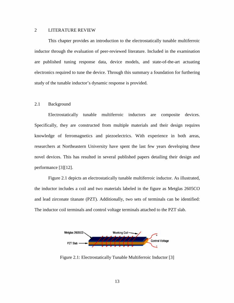
Figure 2.1 depicts an electrostatically tunable multiferroic inductor. As illustrated,
the inductor includes a coil and two materials labeled in the figure as Metglas 2605CO
and lead zirconate titanate (PZT). Additionally, two sets of terminals can be identified:
The inductor coil terminals and control voltage terminals attached to the PZT slab.
Figure 2.1: Electrostatically Tunable Multiferroic Inductor [3]

14
At the core of the inductor are the ferromagnetic and piezoelectric materials, or
Metglas and PZT. Metglas is a magnetoelastic ribbon that possesses a variable
permeability when strained by a mechanical force [3][13]. Conversely, lead zirconate
titanate, or PZT, provides a mechanical strain when subject to an electrical charge [14].
As a composite, the interaction of the two materials forms the magnetoelectric (ME)
effect where the injection of charge into the PZT creates a coupling strain to the Metglas
to vary the permeability. Thus, by wrapping the composite material in a coil of wire, the
PZT/Metglas combination acts as a permeable inductor core with a permeability that is
controlled by the PZT charge.
When changing the permeability of the multiferroic inductor’s core, a change in
inductance is realized [3]. This is illustrated by reviewing the constituent equations that
define permeability and its relationship to inductance. The dynamic permeability of a
ferromagnetic material is defined incrementally as
𝜇𝑑 =𝜕𝐵𝜕𝐻
(2.1)
where 𝐵 is the magnetic flux density of the core and 𝐻 is the magnetic field [15]. If the
ferromagnetic material is a linear device with no hysteresis, equation 2.1 can be
simplified to
𝜇𝑠 =𝐵𝐻
(2.2)
which describes static permeability. Similarly, the incremental, or dynamic, inductance
can be defined as
𝐿𝑑 =𝜕Φ𝜕𝑖
(2.3)
and the inductance of a linear, or static, device can be expressed as

15
𝐿𝑠 =Φ𝑖
(2.4)
where Φ is the magnet flux through the inductor core and 𝑖 is the current through the wire
[15][16].
Assuming a linear time-invariant (LTI) inductor with 𝑁 ideal coil windings and a
multiferroic core material, the permeability in equation 2.2 and the inductance in equation
2.4 are related by the equation for inductance of a multiferroic inductor [3], or
𝐿 =𝜇 ∙ 𝑁2 ∙ 𝐴
𝑙 (2.5)
where 𝐴 is the cross-sectional area of the inductor core and 𝑙 is the length of the solenoid
formed by the stacking of 𝑁 coils. Rearranging equation 2.5 for the permeability results
in
𝜇 =𝐿 ∙ 𝑙𝑁2 ∙ 𝐴
(2.6)
Based on the LTI assumption and citing the definition of static inductance, substituting
equation 2.4 into equation 2.6 produces
𝜇 =Φ𝑖∙
𝑙𝑁2 ∙ 𝐴
(2.7)
Finally, the second product in equation 2.7 can be condensed into a constant term,
resulting in
𝜇 =Φ𝑖∙ 𝐶 = 𝐿𝑠 ∙ 𝐶 (2.8)
where 𝐶 = 𝑙𝑁2∙𝐴
. From equation 2.8 it can be observed that permeability is linearly
proportional to inductance by some constant 𝐶 representing the geometric design of the
inductor. Thus, a change in permeability will result in a proportional inductance change.
16
If non-linear inductance is analyzed, the terms in equation 2.8 can be expressed with their
dynamic counterparts, or
𝜇𝑑 = 𝐿𝑑 ∙ 𝐶 =𝜕𝐵𝜕𝐻
=𝜕Φ𝜕𝑖
∙ 𝐶 (2.9)
thereby suggesting that the slope of the B-H curve is proportional to the slope of the
Φ− 𝑖 curve.
2.2 Performance
While the device has a unique design that requires a fundamental understanding
of device physics, materials science, and electromagnetics, its importance lies in the
performance. The electrostatically tunable multiferroic inductors fabricated at
Northeastern University achieve documented improvement in two of the performance
categories referenced in chapter 1. Both the tuning range and quality factor are improved
over other tunable inductor technologies. Since the tuning speed is currently unreported, a
similar device with published tuning speed is referenced for completion.
2.2.1 Tuning Range
Figure 2.2 on the next page dictates the inductance versus frequency for various
PZT input voltages applied to a laboratory fabricated multiferroic tunable inductor. Each
line color represents a different electric field applied to the PZT with units of 𝑘𝑉𝑐𝑚
, which
can also be represented as volts when the thickness of the PZT is known.

17
Figure 2.2: Multiferroic Inductor Inductance [3]
Given the properties of this particular PZT sample, the electric field in Figure 2.2
represents voltages from 0 to 600 V while producing inductances that range from 0.03 to
0.2 mH. As presented, the inductance plots suggest a tunable range of 450%, 250%, and
50% when operating at 100 Hz, 100 kHz, and 5 MHz respectively. Figure 2.3 reveals
additional tenability data measured by Lou, et al [3].
Figure 2.3: Multiferroic Inductor Tunability [3]
18
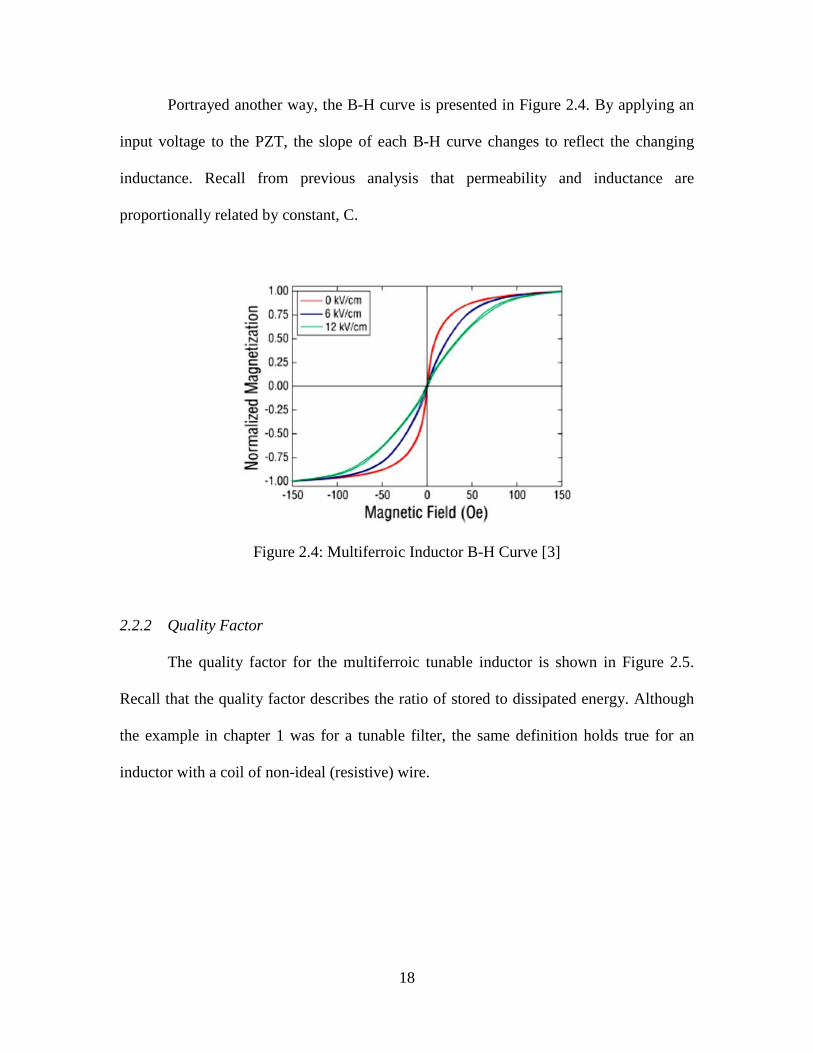
Portrayed another way, the B-H curve is presented in Figure 2.4. By applying an
input voltage to the PZT, the slope of each B-H curve changes to reflect the changing
inductance. Recall from previous analysis that permeability and inductance are
proportionally related by constant, C.
Figure 2.4: Multiferroic Inductor B-H Curve [3]
2.2.2 Quality Factor
The quality factor for the multiferroic tunable inductor is shown in Figure 2.5.
Recall that the quality factor describes the ratio of stored to dissipated energy. Although
the example in chapter 1 was for a tunable filter, the same definition holds true for an
inductor with a coil of non-ideal (resistive) wire.

19
Figure 2.5: Multiferroic Inductor Quality Factor [3]
Based on the graphic, the quality factor ranges from roughly 3 at zero electric field to 8.5
with a voltage applied to the PZT terminals, which is a marked improvement over
competing inductor technologies [3]. Similar to the tunability, the quality factor contains
peaks that vary with frequency.
2.2.3 Tuning Speed
The last performance characteristic to review is the tuning speed. As discussed,
little information exists regarding the transient response of multiferroic devices, and, in
particular, the multiferroic tunable inductor. However, researchers at Northeastern
University have studied the short-term and long-term dynamic performance of a
multiferroic heterostructure and published results describing the change in the
magnetoelectric effect over time [17][18].
In the first document [17], a Metglas/PZT heterostructure was exposed to a high-
voltage square wave switching at a frequency of 0.4 Hz. The input signal was applied for

20
1000 cycles and the magnetoelectric effect was observed via a vibrating sample
magnetometer. The result indicates the magnetoelectric effect features a nonlinear aging
process, thereby causing the permeability associated with a given control voltage to drift
over time as well. As reported by Chen, et al. [17], the aging effect can be attributed to
the physical construction of the heterostructure (bonding), relaxation of the Metglas
ribbon, or ion relaxation of the PZT crystal. While not explicitly investigated, these
findings suggest that the interaction of the physical structure of the multiferroic
heterostructure may have other impacts on temporal dynamics, including tuning speed.
In the second paper, Chen, et al. [18] generally defined the magnetoelectric effect
and studied a PZT/Metglas heterostructure’s transient characteristics in response to an
800 V peak-to-peak step input voltage applied to the PZT. The magnetoelectric effect
was found to fully settle within 0.6 seconds of the applied input voltage, thereby
indicated a 0.6 second tuning response time.
A research group at Oakland University has documented the switching speed of a
multiferroic heterostructure formed by ferromagnetic YIG and ferroelectric barium
strontium titanate (BST) [19]. In this research, a 500 V step voltage was applied to the
BST terminals with rise and fall times of 15 ns to generate a change in the resonate
frequency produced by the YIG/BST composite. The fabricated microwave resonator
experienced a full variation in resonate frequency 100 – 200 µs after application of the
step voltage. The settling time was mainly dictated by the resistor-capacitor (RC) circuit
formed by the input electrode and the BST plate capacitance.
In another study by the same group, a microwave resonator was constructed with
ferromagnetic YIG and piezoelectric PZT [20]. The results indicate a switching time in

21
the low microsecond range. A notable improvement over the YIG/BST resonator, the
decreased settling time can be attributed to the greater than order of magnitude electrode
thickness (more conductivity, or less resistance) and reduced voltage applied to the
YIG/PZT sample (20 V).
2.3 Modeling
To properly realize the stated hypothesis, the multiferroic tunable inductor’s
physical behavior must be modeled mathematically to facilitate the design of actuating
electronics. Without a model, one may have difficulty specifying the type of load a
tunable inductor’s control terminals present to an external amplifier, thereby reducing
optimal tuning speed. Since the direct interface to an amplifier output is the PZT control
terminals, published piezoelectric circuit models are discussed with arbitrary mechanical
loads. Research regarding Metglas and time-varying inductance modeling is also
discussed.
2.3.1 Piezoelectric
The classic piezoelectric circuit model is the Butterworth Van Dyke (BVD) model
presented schematically in Figure 2.6 [21].

22
Figure 2.6: Butterworth Van Dyke Piezoelectric Circuit Model
The BVD model is comprised of a capacitor (C0) in parallel with a series resistor-
inductor-capacitor (RLC) circuit. The dominant parallel capacitance (C0) approximates
the crystal dielectric separating the PZT terminals. The additional RLC components are
necessary to model the mechanical resonance of the PZT. The electrical equivalents are
described as resistor RM (damping coefficient), inductor LM (equivalent mass), and
capacitor CM (spring constant).
The model suggests primarily capacitive behavior over frequency due to C0. The
resonant peak, however, must be accounted for if control input frequencies will sweep
through the resonance band. Figure 2.7 illustrates the impedance magnitude to enlighten
these points. The data was collected by Guan, et al. [21] for a 500 µm thick PZT sample
from Piezo Systems, Inc. and incorporated into a Simulation Program with Integrated
Circuit Emphasis (SPICE) simulation to produce the plot.
C0
RM
LM
CM
INO
UT
23
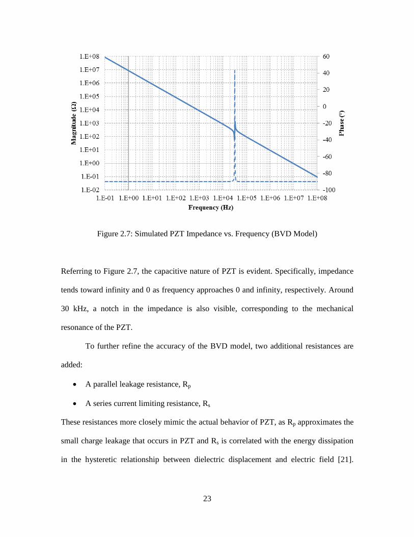
Figure 2.7: Simulated PZT Impedance vs. Frequency (BVD Model)
Referring to Figure 2.7, the capacitive nature of PZT is evident. Specifically, impedance
tends toward infinity and 0 as frequency approaches 0 and infinity, respectively. Around
30 kHz, a notch in the impedance is also visible, corresponding to the mechanical
resonance of the PZT.
To further refine the accuracy of the BVD model, two additional resistances are
added:
• A parallel leakage resistance, Rp
• A series current limiting resistance, Rs
These resistances more closely mimic the actual behavior of PZT, as Rp approximates the
small charge leakage that occurs in PZT and Rs is correlated with the energy dissipation
in the hysteretic relationship between dielectric displacement and electric field [21].

24
Accounting for the additional resistances results in simulated responses plotted in Figure
2.8 and 2.9.
Figure 2.8: Simulated Impedance Magnitude vs. Frequency
Figure 2.9: Simulated Impedance Phase vs. Frequency

25
The dashed line is the Guan impedance that features magnitude limits and phase shifting
as frequency tends towards 0 and infinity, substantiating the Guan model as a more
realistic model.
The above data was compiled for an unloaded sample that features a single
resonant mode. If the PZT is bonded to another material, however, the mechanical
boundary conditions are changed [21]. This alteration produces additional modes which
must be accounted for in the model. Thus, Guan, et al. [21], proposed additional parallel
RLC circuits to model the increased resonance frequencies. Figure 2.10 provides a
schematic representation of fully loaded Guan piezoelectric model with three resonant
modes.
Figure 2.10: Guan Piezoelectric Circuit Model with Mechanical Loading
The dominant capacitive nature of PZT results in some designers choosing to
model the piezoelectric device as a single capacitor [22]. Care must be taken to ensure
C0
R1
L1
C1
Rs
Rp
R2
L2
C2
R3
L3
C3
INOU
T

26
that input frequencies do not excite the resonant modes; else the behavior will take on
second-order effects. This effect can be readily seen when dealing with step input, square
wave, and switching voltages that feature fast rise and fall times [23].
2.3.2 Ferromagnetic
As reported by Chen, et al. [18], the response of the Metglas to a mechanical
strain is on the order of a microsecond. Therefore, its dynamics may be assumed
negligible until the response of the PZT approaches within an order of magnitude or less
(i.e., 10 µs).
2.3.3 Time-Varying Inductance
Another important aspect of the tunable inductor that requires modeling is the
time-varying inductance formed by the interaction of a wire coil and the Metglas/PZT
heterostructure. Assuming an LTI core, researchers at the University of Defence Brno
discussed the proper modeling of a time-varying inductance for use in SPICE circuit
simulations [24]. While geared toward computer simulation, the derived mathematics
hold true.
The literature indicates standard textbook equations that define the voltage across
the terminals of an inductor do not persist when dealing with an inductor that changes
values over time. Equation 2.10 presents the voltage across an LTI inductor.
𝑣 = 𝐿 ∙𝑑𝑖𝑑𝑡
(2.10)
If the inductor is time-varying, however, the expression changes to [24]

27
𝑣(𝑡) = 𝐿(𝑡) ∙𝑑𝑖𝑑𝑡
+ 𝑖(𝑡) ∙𝑑𝐿𝑑𝑡
(2.11)
After integrating, the expression for computing inductance is
𝐿(𝑡) =𝐿(0) ∙ 𝑖(0) + ∫ 𝑣(𝑡) ∙ 𝑑𝑡𝜏
0𝑖(𝑡)
(2.12)
Biolek, et al. [24] assert that equation 2.12 should be applied to situations where an
inductance is time-varying.
2.4 Actuation
To deliver the proper charge to the PZT plates, high-performance driver circuits
are necessary. As discussed, PZT devices require hundreds of volts to achieve a
displacement that appropriately strains the Metglas, thus affecting the permeability. If the
PZT/Metglas heterostructure is modeled as a mechanically loaded PZT sample, research
published in the piezoelectric driver domain may be useful in assessing state-of-the-art
driver circuit technology.
A number of amplifiers were surveyed, and each device was selected to compare
performance in four key categories:
• Voltage
o Sufficient to displace the PZT and bonded Metglas to modify Metglas
permeability, thus producing a tunable inductance. Based on previous
research [3], greater than 100 V is preferred.
• Current

28
o Sufficient to supply charge to the PZT plates consistent with the desired
tuning speed (frequency). Based on PZT modeling, greater than 2 A is
preferred.
• Slew Rate
o If several hundred volts are required to tune the inductor to the desired
frequency, and this tuning value is requested on the order of a few
microseconds, a slew-rate approaching 100 V/µs is desirable.
• Bandwidth
o In high-frequency applications, varying inductance may necessary at
differing periods. To switch frequencies in this fashion, higher bandwidth
amplifiers are desirable.
In Table 2.1 on the subsequent page, the best of the surveyed driver circuit
specifications are compared to determine if a published amplifier suits the above
requirements.
29
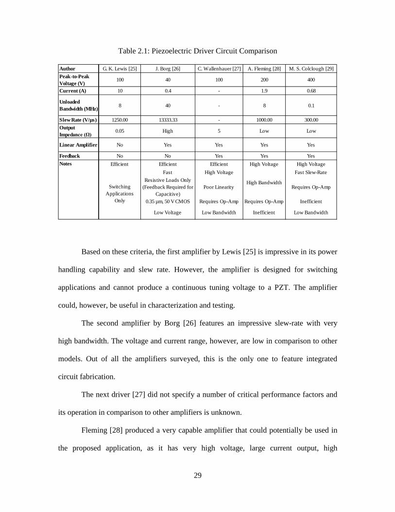
Table 2.1: Piezoelectric Driver Circuit Comparison
Based on these criteria, the first amplifier by Lewis [25] is impressive in its power
handling capability and slew rate. However, the amplifier is designed for switching
applications and cannot produce a continuous tuning voltage to a PZT. The amplifier
could, however, be useful in characterization and testing.
The second amplifier by Borg [26] features an impressive slew-rate with very
high bandwidth. The voltage and current range, however, are low in comparison to other
models. Out of all the amplifiers surveyed, this is the only one to feature integrated
circuit fabrication.
The next driver [27] did not specify a number of critical performance factors and
its operation in comparison to other amplifiers is unknown.
Fleming [28] produced a very capable amplifier that could potentially be used in
the proposed application, as it has very high voltage, large current output, high
Author G. K. Lewis [25] J. Borg [26] C. Wallenhauer [27] A. Fleming [28] M. S. Colclough [29]Peak-to-Peak Voltage (V)
100 40 100 200 400
Current (A) 10 0.4 - 1.9 0.68
Unloaded Bandwidth (MHz) 8 40 - 8 0.1
Slew Rate (V/µs) 1250.00 13333.33 - 1000.00 300.00Output Impedance (Ω)
0.05 High 5 Low Low
Linear Amplifier No Yes Yes Yes Yes
Feedback No No Yes Yes YesEfficient Efficient Efficient High Voltage High Voltage
Fast High Voltage Fast Slew-RateResistive Loads Only
(Feedback Required for Capacitive)
Poor Linearity Requires Op-Amp
0.35 µm, 50 V CMOS Requires Op-Amp Requires Op-Amp Inefficient
Low Voltage Low Bandwidth Inefficient Low Bandwidth
Notes
Switching Applications
Only
High Bandwidth

30
bandwidth, and fast slew-rate. The amplifier is based on an Apex Microtechnology power
amplifier, and a discrete transistor output stage.
Finally, Colclough [29] advertised an amplifier that achieved impressive voltage,
but was lacking in other categories.
Given the above data, the amplifier by Fleming is most suited for driving the
tunable inductor. It’s possible, however, that the current rating may not be sufficient for
providing the necessary PZT charge. This fact will be considered in later chapters.

31
3 METHODOLOGY
The literature in the previous chapter provides a foundation from which the tuning
response time of a tunable inductor may be theoretically analyzed and experimentally
measured. In this chapter, the study of electrostatically tunable multiferroic inductors is
advanced through
• the development of mathematics that describe and simulate the interaction
between the piezoelectric material and the time-varying inductance.
• the development of appropriate actuating electronics.
• novel laboratory measurement techniques to capture the changing inductance over
time.
The research builds upon cited literature in an attempt to further the development of
electrostatically tunable multiferroic inductors and multiferroic heterostructures in
general.
3.1 Electrostatically Tunable Multiferroic Inductor Dynamics
The goal of this section is to develop a method for accurately measuring a
changing inductance over time. In doing so, the tuning speed of the multiferroic inductor
may be established. To determine the tuning response of a tunable inductor, however, a
measureable parameter must first be identified that properly conveys the variation in
tunability. A seemingly obvious parameter that lends itself to measurement is the
inductance itself, as inductors are well defined in circuit analysis textbooks [8][15]. To
properly measure the inductance of an electrostatically tunable mutliferroic inductor,
32
however, the physical behavior of the PZT and Metglas must be understood, as well as
the mathematical equations that represent this behavior.
In chapter two, the physical behavior of the PZT/Metglas permeable core was
discussed to gain insight into how the PZT and Metglas react to step voltages applied to
the control inputs. The following paragraphs further this work by analyzing the dynamic
properties of PZT and Metglas and how they relate to measuring inductance through
mathematical analysis and simulation.
3.1.1 Linear Time-Invariant Inductor
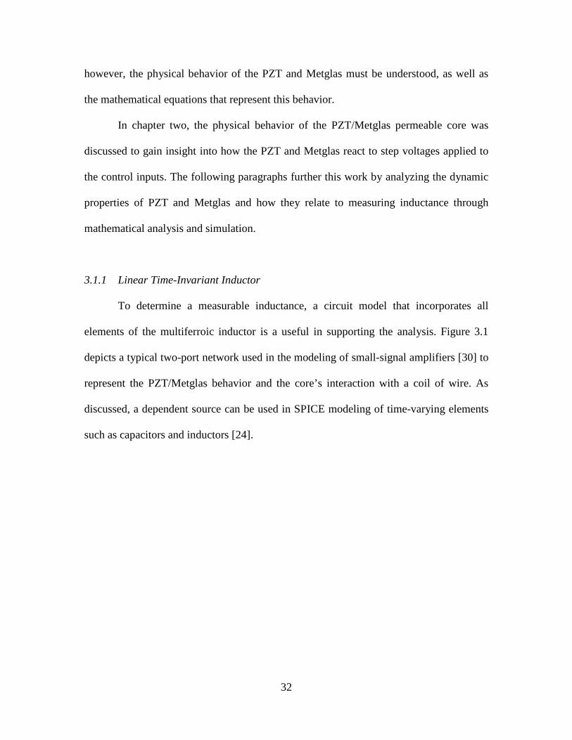
To determine a measurable inductance, a circuit model that incorporates all
elements of the multiferroic inductor is a useful in supporting the analysis. Figure 3.1
depicts a typical two-port network used in the modeling of small-signal amplifiers [30] to
represent the PZT/Metglas behavior and the core’s interaction with a coil of wire. As
discussed, a dependent source can be used in SPICE modeling of time-varying elements
such as capacitors and inductors [24].
33
Figure 3.1: Two-Port Network
In Figure 3.1, element Z on the left side of the schematic represents the PZT electrical
impedance seen by a driving source. On the right is a dependent current source that
represents the inductor current as a function of the terminal voltage, Vo. In other words,
any load connected across the inductor that applies a voltage, Vo, will experience a
current through it dictated by f(Vo) and vice versa.
The function f(Vo) can be expanded more explicitly to describe the inductor
current dependence on voltage. The terminal voltage of an inductor is related to current
through Faraday’s law, which states that the time derivative of magnetic flux, Φ, is
equivalent to the voltage across an inductors terminals, or
𝑣 =𝑑Φ𝑑𝑡
(3.1)
Since the magnetic flux is equivalent to the product of inductance and current through the
inductor as described by equation 2.4, equation 3.1 expands to
i=f(Vo)Z VoVi
34
𝑣 =𝑑(𝐿 ∙ 𝑖)𝑑𝑡
= 𝐿 ∙𝑑𝑖𝑑𝑡
(3.2)
The expression in equation 3.2 implies that the inductance can be determined if the
voltage and current are measurable. With the proper laboratory setup, voltage and current
are measurable and 𝐿 can be extracted by dividing the voltage time-series by the current
derivative. Or, equation 3.2 can be integrated to obtain
𝑖(𝑡) = 𝑖(𝑡0) +1𝐿� 𝑣(𝑡) ∙ 𝑑𝑡 = 𝑓(𝑉𝑜)𝑡
𝑡0 (3.3)
which satisfies the dependent source relationship in Figure 3.1. In equation 3.3, the
inductance is found by integrating the voltage-time series and dividing by the current
time-series minus the initial current value.
There are fundamental flaws with the presented scenario, however. Noticeably
absent is any relationship between the input Vi and Z to the output dependent source.
Modeling the inductance in this way fails to capture the inductor’s true dependence on
permeability, µ, as described in equation 2.5. Further, the assumption in this section is the
inductor behavior is linear and time-invariant (LTI). As will be shown in the next section,
time invariance is not preserved when modeling the relationship from input to output in
Figure 3.1, and additional steps must be taken to properly extract the inductance value.
3.1.2 Linear Time-Variant Inductor
Referring back to Figure 3.1, the permeability of the Metglas – and, ultimately,
the inductance – can be shown to depend on the PZT impedance. More importantly, the
permeability will be shown to change over time and cause a violation in the time-
invariant assumption of the LTI inductor presented above.

35
To begin, Figure 3.1 can be modified to illustrate a direct depiction of inductance.
Figure 3.2: Modified Two-Port Network
In Figure 3.2, the dependent source is replaced directly by an inductor that is a function
of permeability. The inductance of a multiferroic tunable inductor was previously
investigated by Lou, et al. [3] as
𝐿 =𝜇 ∙ 𝑁2 ∙ 𝐴
𝑙 (3.4)
with permeability plainly influencing the inductance value. Additionally, the impedance
of the PZT material was researched by Guan, et al. [21] and found to be
𝑍(𝑠) =𝑠2 ∙ 𝐿𝑀 ∙ 𝐶𝑀 + 𝑠 ∙ 𝑅𝑀 ∙ 𝐶𝑀 + 1
𝑠3 ∙ 𝐿𝑀 ∙ 𝐶0 ∙ 𝐶𝑀 + 𝑠2 ∙ 𝑅𝑀 ∙ 𝐶0 ∙ 𝐶𝑀 + 𝑠 ∙ (𝐶𝑀 + 𝐶0) (3.5)
for the BVD model.
To relate the impedance in equation 3.5 to the current-voltage characteristics of
the inductor in Figure 3.2, the charge of the PZT is analyzed. As mentioned, the strain
ZVi VoLL=f(u)

36
provided by PZT is related to the amount of charge on its plates. The impedance seen by
a source driving the PZT, however, dictates the amount of charge transferred to the PZT
plates. This is explained by the following Laplace-domain expression for impedance,
which states that the ratio of voltage to current is equal to impedance, or
𝑍(𝑠) =𝑉(𝑠)𝐼(𝑠) ⇒ 𝐼(𝑠) =
𝑉(𝑠)𝑍(𝑠)
(3.6)
Also suggested in equation 3.6 is that the ratio of voltage to impedance yields the current
flow. Given that the impedance of the PZT for the BVD model was provided, substituting
into equation 3.6 yields
𝐼(𝑠) =𝑉(𝑠) ∙ 𝑠 ∙ 𝐶𝑀
𝑠2 ∙ 𝐿𝑀 ∙ 𝐶𝑀 + 𝑠 ∙ 𝑅𝑀 ∙ 𝐶𝑀 + 1+ 𝑉(𝑠) ∙ 𝑠 ∙ 𝐶0 (3.7)
Since current is equivalent to the quantity of charge transferred through a point in an
electric circuit per second, current and charge are related by
𝑞𝑃𝑍𝑇(𝑡) − 𝐶𝑖𝑛𝑡𝑒𝑔𝑟𝑎𝑡𝑖𝑜𝑛 = �𝑖(𝑡) ∙ 𝑑𝑡 (3.8)
Equation 3.8 demonstrates that the time integral of current will sum the amount of charge
transferred to the PZT plates, 𝑞𝑃𝑍𝑇(𝑡). Since impedance was provided in the Laplace
domain, using the Laplace property of integration will return equation 3.8 to the proper
domain. Assuming the no charge is present on the plates as an initial condition
(𝐶𝑖𝑛𝑡𝑒𝑔𝑟𝑎𝑡𝑖𝑜𝑛 = 0), the following relationships are defined.
ℒ{𝑞𝑃𝑍𝑇(𝑡)} = 𝑄𝑃𝑍𝑇(𝑠) (3.9)
ℒ �� 𝑖(𝑡) ∙ 𝑑𝑡� =1𝑠∙ 𝐼(𝑠) (3.10)
𝑄𝑃𝑍𝑇(𝑠) =1𝑠∙ 𝐼(𝑠) (3.11)
37
Equations 3.9, 3.10, and 3.11 illustrate the Laplace transformation of time domain charge
to its Laplace domain equivalent, 𝑄𝑃𝑍𝑇(𝑠) . Current flow to the PZT in the Laplace
domain is now divided by the Laplace variable, 𝑠, and equated to charge.
By further substitution, the PZT charge can be related to the voltage and
impedance ratio in equation 3.6 by
𝑄𝑃𝑍𝑇(𝑠) =1𝑠∙ 𝐼(𝑠) =
1𝑠∙𝑉(𝑠)𝑍(𝑠)
(3.12)
Multiplication of the 1𝑠 term into equation 3.12 allows for cancelling of common terms
after expanding 𝑍(𝑠), yielding
𝑄𝑃𝑍𝑇(𝑠) = 𝑉(𝑠) ∙ 𝐶𝑀
𝑠2 ∙ 𝐿𝑀 ∙ 𝐶𝑀 + 𝑠 ∙ 𝐶𝑀 ∙ 𝑅𝑀 + 1+ 𝑉(𝑠) ∙ 𝐶0 (3.13)
Not surprisingly, after converting from the Laplace domain to the frequency domain by
substituting 𝑗𝜔 for 𝑠, the expression confirms that charge across the PZT plates at 0 Hz
(DC) is equivalent to
𝑄𝑃𝑍𝑇(0) = 𝑉(0) ∙ 𝐶𝑀 + 𝑉(0) ∙ 𝐶0 = 𝑉(0) ∙ (𝐶𝑀 + 𝐶0) (3.14)
or, the steady-state voltage multiplied by the total capacitance of the PZT plates.
Additionally, by dividing the numerator and denominator of the first term in equation
3.13 by 𝐿𝑀 ∙ 𝐶𝑀 and dividing both sides by 𝑉(𝑠), the low-pass form is similar to equation
1.3 discussed in chapter 1, plus a capacitive offset.
𝑃(𝑠) =𝑄𝑃𝑍𝑇(𝑠)𝑉(𝑠) = 𝐶𝑀
1𝐿𝑀 ∙ 𝐶𝑀
𝑠2 + 𝑠 ∙ 𝑅𝑀𝐿𝑀+ 1𝐿𝑀 ∙ 𝐶𝑀
+ 𝐶0 (3.15)
The quality factor of frequency domain charge is similar to that of the band-pass filter
discussed in chapter one. Given that 𝑅𝑀 is usually several orders of magnitude larger than
38
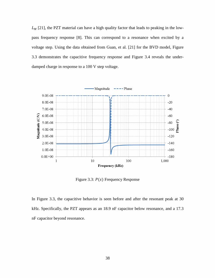
𝐿𝑀 [21], the PZT material can have a high quality factor that leads to peaking in the low-
pass frequency response [8]. This can correspond to a resonance when excited by a
voltage step. Using the data obtained from Guan, et al. [21] for the BVD model, Figure
3.3 demonstrates the capacitive frequency response and Figure 3.4 reveals the under-
damped charge in response to a 100 V step voltage.
Figure 3.3: 𝑃(𝑠) Frequency Response
In Figure 3.3, the capacitive behavior is seen before and after the resonant peak at 30
kHz. Specifically, the PZT appears as an 18.9 nF capacitor below resonance, and a 17.3
nF capacitor beyond resonance.

39
Figure 3.4: Simulated PZT Charge Step Response
In Figure 3.4, as expected, the charge settles to a steady-state value relative to the total
capacitance of the PZT and the voltage applied to the plates, or
100 𝑉 ∙ (17.3 𝑛𝐹 + 1.6 𝑛𝐹) = 100 𝑉 ∙ (18.9 𝑛𝐹) = 1.89 𝜇𝐶
Since it was previously determined that PZT produces a strain in relation to an
applied charge, the following general association is defined:
𝐴𝑃𝑍𝑇(𝑠) =𝑆𝑃𝑍𝑇(𝑠)𝑄𝑃𝑍𝑇(𝑠) (3.16)
Equation 3.16 states mathematically what was described in the aforementioned
paragraph, where 𝑆𝑃𝑍𝑇 is the strain produced by the charge, 𝑄𝑃𝑍𝑇(𝑠) , and 𝐴𝑃𝑍𝑇(𝑠)
describes the relationship between strain and charge. Consistent with published analysis,
𝐴𝑃𝑍𝑇(𝑠) is equivalent to the g constant that describes the strain developed over an applied

40
charge density with units of meters squared per coulomb [32]. Therefore, the Laplace
variable 𝑠 can be dropped and 𝐴𝑃𝑍𝑇 treated as a coefficient for further analysis, or
𝐴𝑃𝑍𝑇(𝑠) = 𝐴𝑃𝑍𝑇 (3.17)
Similarly, a coupling factor can be introduced to describe the relationship between
the PZT and Metglas strain, or
𝐴𝑃𝑍𝑇/𝑀𝑒𝑡𝑔𝑙𝑎𝑠(𝑠) =𝑆𝑀𝑒𝑡𝑔𝑙𝑎𝑠(𝑠)𝑆𝑃𝑍𝑇(𝑠) (3.18)
where 𝑆𝑀𝑒𝑡𝑔𝑙𝑎𝑠(𝑠) and 𝐴𝑃𝑍𝑇/𝑀𝑒𝑡𝑔𝑙𝑎𝑠(𝑠) are the strain experienced by the Metglas and the
coupling factor, respectively. Assuming that equal strain is applied to the entire surface of
the Metglas and the bonding material does not introduce dynamic effects,
𝐴𝑃𝑍𝑇/𝑀𝑒𝑡𝑔𝑙𝑎𝑠(𝑠) represents a coefficient that describes the amount of deflection
transferred from one material to the other. For example, a value of one would indicate
full transfer of strain. Hence, the Laplace variable 𝑠 in 𝐴𝑃𝑍𝑇/𝑀𝑒𝑡𝑔𝑙𝑎𝑠 is dropped for further
analysis, or
𝐴𝑃𝑍𝑇/𝑀𝑒𝑡𝑔𝑙𝑎𝑠(𝑠) = 𝐴𝑃𝑍𝑇/𝑀𝑒𝑡𝑔𝑙𝑎𝑠 (3.19)
Finally, a relationship between the strain on the Metglas and its permeability can
be established as
𝐴𝑀𝑒𝑡𝑔𝑙𝑎𝑠(𝑠) =𝑀𝑀𝑒𝑡𝑔𝑙𝑎𝑠(𝑠)𝑆𝑀𝑒𝑡𝑔𝑙𝑎𝑠(𝑠) (3.20)
where 𝑀𝑀𝑒𝑡𝑔𝑙𝑎𝑠(𝑠) and 𝐴𝑀𝑒𝑡𝑔𝑙𝑎𝑠(𝑠) are the Laplace domain permeability of Metglas and
gain of the strain to permeability ratio. Given the research by Chen, Harris, et al. [18], it
was shown that the Metglas has a very fast response time on the order of one
microsecond. Assuming a first-order response, the transfer function in equation 3.20 will

41
have a time constant approximately 5 times less1 than one µs, or no greater than 200 ns.
Placing equation 3.20 into the form of a general first-order transfer function yields
𝐴𝑀𝑒𝑡𝑔𝑙𝑎𝑠(𝑠) =1
𝑠 ∙ 𝜏 + 1 (3.21)
with 𝜏 signifying the time constant in seconds [8]. Given this first-order low-pass filter
transfer function, the 1/𝜏 pole location is no less than 5 MHz. By this assumption, the
pole due to the Metglas strain will not likely influence the lower frequency poles
introduced by the PZT impedance, and 𝐴𝑀𝑒𝑡𝑔𝑙𝑎𝑠(𝑠) can be assumed a constant, or
𝐴𝑀𝑒𝑡𝑔𝑙𝑎𝑠(𝑠) = 𝐴𝑀𝑒𝑡𝑔𝑙𝑎𝑠 (3.22)
Given equations 3.16, 3.18, and 3.20, the permeability of Metglas can be related
back to the charge across the PZT plates by making the following substitutions. First,
multiply both sides of equation 3.20 by the strain term, 𝑆𝑀𝑒𝑡𝑔𝑙𝑎𝑠(𝑠), and divide by the
constant 𝐴𝑀𝑒𝑡𝑔𝑙𝑎𝑠 to create the following expression:
𝑆𝑀𝑒𝑡𝑔𝑙𝑎𝑠(𝑠) =𝑀𝑀𝑒𝑡𝑔𝑙𝑎𝑠(𝑠)𝐴𝑀𝑒𝑡𝑔𝑙𝑎𝑠
(3.23)
Substituting the above expression into equation 3.18 yields
𝐴𝑃𝑍𝑇/𝑀𝑒𝑡𝑔𝑙𝑎𝑠 =𝑀𝑀𝑒𝑡𝑔𝑙𝑎𝑠(𝑠)
𝐴𝑀𝑒𝑡𝑔𝑙𝑎𝑠 ∙ 𝑆𝑃𝑍𝑇(𝑠) (3.24)
and rearranging for 𝑆𝑃𝑍𝑇(𝑠) produces
𝑆𝑃𝑍𝑇(𝑠) =𝑀𝑀𝑒𝑡𝑔𝑙𝑎𝑠(𝑠)
𝐴𝑃𝑍𝑇/𝑀𝑒𝑡𝑔𝑙𝑎𝑠 ∙ 𝐴𝑀𝑒𝑡𝑔𝑙𝑎𝑠 (3.25)
Substituting for 𝑆𝑃𝑍𝑇(𝑠) by the ratio in equation 3.16 yields
1 After five time constants, a first-order system will have achieved approximately 99% of its final value [8]

42
𝐴𝑃𝑍𝑇 =𝑀𝑀𝑒𝑡𝑔𝑙𝑎𝑠(𝑠)
𝐴𝑃𝑍𝑇/𝑀𝑒𝑡𝑔𝑙𝑎𝑠 ∙ 𝐴𝑀𝑒𝑡𝑔𝑙𝑎𝑠 ∙ 𝑄𝑃𝑍𝑇(𝑠) (3.26)
Rearranging the constant terms to the left-hand side of equation 3.26 gives the following
expression relating charge to strain:
𝐴𝑃𝑍𝑇 ∙ 𝐴𝑃𝑍𝑇/𝑀𝑒𝑡𝑔𝑙𝑎𝑠 ∙ 𝐴𝑀𝑒𝑡𝑔𝑙𝑎𝑠 = 𝐴 =𝑀𝑀𝑒𝑡𝑔𝑙𝑎𝑠(𝑠)𝑄𝑃𝑍𝑇(𝑠) (3.27)
Multiplying both sides of equation 3.27 by 𝑄𝑃𝑍𝑇(𝑠) illustrates how the permeability
response is a scaled replica of the charge response.
𝐴 ∙ 𝑄𝑃𝑍𝑇(𝑠) = 𝑀𝑀𝑒𝑡𝑔𝑙𝑎𝑠(𝑠) (3.28)
Since 𝐴𝑃𝑍𝑇, 𝐴𝑃𝑍𝑇/𝑀𝑒𝑡𝑔𝑙𝑎𝑠, and 𝐴𝑀𝑒𝑡𝑔𝑙𝑎𝑠 are all constant values, they are consolidated into
a single variable, 𝐴, to represent a coupling gain factor. The gain may be positive or
negative. According to Lou, et al. [3], the increased charge in PZT decreases permeability
due to negative coefficients, implying 𝐴 will be negative.
One final relationship can be established from the above analysis: The impedance
term, 𝑍(𝑠) , and the actuating electronics driving voltage, 𝑉(𝑠) , can be inserted into
equation 3.28 to form a complete expression from voltage input to permeability output.
Substituting equation 3.5 into equation 3.28 yields
𝐴 =𝑀𝑀𝑒𝑡𝑔𝑙𝑎𝑠(𝑠)
1𝑠 ∙𝑉(𝑠)𝑍(𝑠)
⇒𝑀𝑀𝑒𝑡𝑔𝑙𝑎𝑠(𝑠)
𝑉(𝑠)=
𝐴𝑠 ∙ 𝑍(𝑠)
(3.29)
and expanding to include the unloaded BVD model results in transfer function 𝑀(𝑠):
𝑀(𝑠) =𝑀𝑀𝑒𝑡𝑔𝑙𝑎𝑠(𝑠)
𝑉(𝑠) (3.30)
43
𝑀(𝑠) = 𝐴 ∙ �𝐶𝑀
1𝐿𝑀 ∙ 𝐶𝑀
𝑠2 + 𝑠 ∙ 𝑅𝑀𝐿𝑀+ 1𝐿𝑀 ∙ 𝐶𝑀
+ 𝐶0� = 𝐴 ∙ 𝑃(𝑠) (3.31)
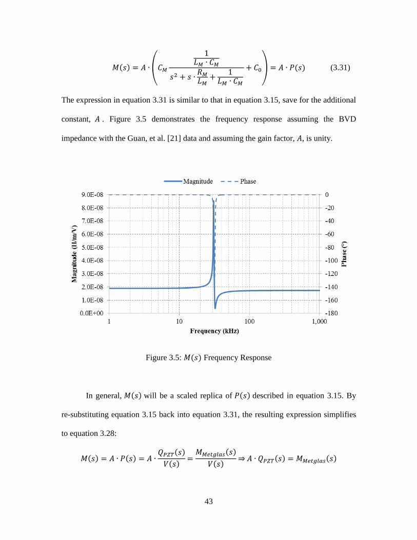
The expression in equation 3.31 is similar to that in equation 3.15, save for the additional
constant, 𝐴 . Figure 3.5 demonstrates the frequency response assuming the BVD
impedance with the Guan, et al. [21] data and assuming the gain factor, 𝐴, is unity.
Figure 3.5: 𝑀(𝑠) Frequency Response
In general, 𝑀(𝑠) will be a scaled replica of 𝑃(𝑠) described in equation 3.15. By
re-substituting equation 3.15 back into equation 3.31, the resulting expression simplifies
to equation 3.28:
𝑀(𝑠) = 𝐴 ∙ 𝑃(𝑠) = 𝐴 ∙𝑄𝑃𝑍𝑇(𝑠)𝑉(𝑠) =
𝑀𝑀𝑒𝑡𝑔𝑙𝑎𝑠(𝑠)𝑉(𝑠) ⇒𝐴 ∙ 𝑄𝑃𝑍𝑇(𝑠) = 𝑀𝑀𝑒𝑡𝑔𝑙𝑎𝑠(𝑠)

44
As a result, 𝜇𝑀𝑒𝑡𝑔𝑙𝑎𝑠(𝑡) is a reflection of 𝑞𝑃𝑍𝑇(𝑡) in the time domain, including all
second-order effects such as overshoot, under-damped oscillations, and settling time [33].
In the time domain expression, the relationship is simply:
𝐴 ∙ 𝑞𝑃𝑍𝑇(𝑡) = 𝜇𝑀𝑒𝑡𝑔𝑙𝑎𝑠(𝑡) (3.32)
It should be noted, however, that if the terms 𝐴𝑃𝑍𝑇 , 𝐴𝑃𝑍𝑇/𝑀𝑒𝑡𝑔𝑙𝑎𝑠 , and 𝐴𝑀𝑒𝑡𝑔𝑙𝑎𝑠 are a
function of Laplace variable 𝑠due to dynamic behavior, additional poles and zeros will be
introduced into the transfer function in equation 3.31. This may alter the dynamic
response and equation 3.31 will no longer hold true.
Finally, it should be noted that the capacitance of piezoelectric material can be
hysteretic [34] and the capacitive terms in equation 3.31 may not always be constant after
a strain has been applied. Thus, permeability may not always reflect a one-to-one
relationship with an applied voltage that strains the PZT in such a way that the hysteresis
curve comes into play.
The main focus of the above analysis is to review time domain response of the
permeability. Once a voltage step input is applied to the PZT, the permeability reacts as a
function of the voltage and may feature overshoot, ringing, and/or settling. Since
permeability of the multiferroic tunable inductor is a demonstrated function of time, the
inductance will also be a function of time, or time-variant.
𝐿(𝑡) =𝜇(𝑡) ∙ 𝑁2 ∙ 𝐴
𝑙 (3.33)
Referring back to equation 3.2, the derivative term no longer simplifies to a product of
the static inductance and the time derivative of the current through the inductor coils.
Rather, it expands to

45
𝑣(𝑡) =𝑑�𝐿(𝑡) ∙ 𝑖(𝑡)�
𝑑𝑡=𝑑𝐿𝑑𝑡
∙ 𝑖(𝑡) +𝑑𝑖𝑑𝑡∙ 𝐿(𝑡) (3.34)
under the assumption that the inductance is still linear.
To move forward and isolate the inductance term such that it may be solved for, a
slightly different approach must be used as 𝐿(𝑡) is no longer a unique variable. One
approach is to integrate both sides of equation 3.34. The result is
𝐿(𝑡0) ∙ 𝑖(𝑡0) + � 𝑣(𝑡) ∙ 𝑑𝑡 = 𝐿(𝑡) ∙ 𝑖(𝑡)𝑡
𝑡0 (3.35)
and rearranging yields
𝐿(𝑡) =𝐿(𝑡0) ∙ 𝑖(𝑡0) + ∫ 𝑣(𝑡) ∙ 𝑑𝑡𝑡
𝑡0𝑖(𝑡)
(3.36)
This expression is identical to that derived by Biolek, et al. [24] in their paper on the
SPICE modeling of time-varying components. In equation 3.36, several constant terms
are generated due to the integration. These terms are 𝐿(𝑡0) and 𝑖(𝑡0), or the inductance
and current values at zero time in the circuit.
Interestingly, if the inductance is time-invariant, or 𝐿(𝑡) = 𝐿(𝑡0) = 𝐿, multiplying
both sides by 𝑖(𝑡) and dividing by 𝐿 yields the familiar circuit expression for current
through an inductor [8] derived in equation 3.3.
𝑖(𝑡) =𝐿(𝑡0) ∙ 𝑖(𝑡0) + ∫ 𝑣(𝑡) ∙ 𝑑𝑡𝑡
𝑡0𝐿(𝑡0)
= 𝑖(𝑡0) +1𝐿� 𝑣(𝑡) ∙ 𝑑𝑡𝑡
𝑡0 (3.37)
Consequently, equation 3.36 provides an expression that allows time-varying
inductance to be computed by measuring the voltage and current at the inductor terminals
and by taking into account any initial conditions that exist. Therefore, the initial
inductance must be known at the time the measurement is started. With this knowledge,

46
any change in permeability via an applied voltage to the PZT inputs will be accurately
represented by equation 3.36 as a measurable inductance change.
Although the above method is suitable for determining inductance, there is
another measurement method worth discussing. In the previous analysis, a sinusoidal
voltage source (or similar) is required to drive the inductor such that a change in
inductance would present a change in the inductor voltage and, thus, a changing
inductance. If, however, the voltage source was modified to a constant current source, the
mathematics simplifies. By equation 3.34, a constant current will zero the derivative term
and leave only the following expression:
𝑣(𝑡) =𝑑𝐿𝑑𝑡
∙ 𝑖(𝑡0) + 0 ∙ 𝐿(𝑡) =𝑑𝐿𝑑𝑡
∙ 𝑖(𝑡0) (3.38)
Whether integrating or deriving from equation 3.38, the resulting measurement equation
is
𝐿(𝑡) =𝐿(𝑡0) ∙ 𝑖(𝑡0) + ∫ 𝑣(𝑡) ∙ 𝑑𝑡𝑡
𝑡0𝑖(𝑡0)
(3.39)
𝐿(𝑡) = 𝐿(𝑡0) +1
𝑖(𝑡0)∙ � 𝑣(𝑡) ∙ 𝑑𝑡
𝑡
𝑡0 (3.40)
Now, when the permeability changes due to some input voltage at the PZT terminals, the
inductance change is reflected solely in the voltage across the inductor terminals. In the
next few sections, the constant current method will reveal its importance to tuning speed
characterization.
47
3.1.3 Linear Time-Varying Multiferroic Inductor Simulation
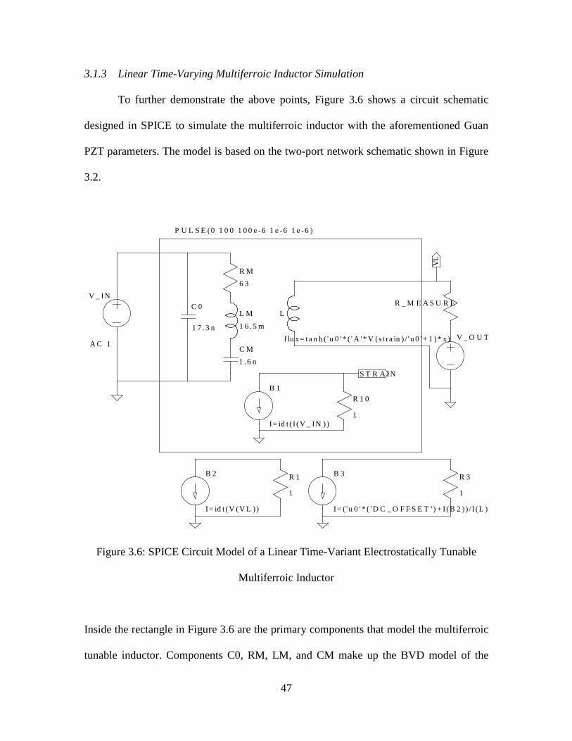
To further demonstrate the above points, Figure 3.6 shows a circuit schematic
designed in SPICE to simulate the multiferroic inductor with the aforementioned Guan
PZT parameters. The model is based on the two-port network schematic shown in Figure
3.2.
Figure 3.6: SPICE Circuit Model of a Linear Time-Variant Electrostatically Tunable
Multiferroic Inductor
Inside the rectangle in Figure 3.6 are the primary components that model the multiferroic
tunable inductor. Components C0, RM, LM, and CM make up the BVD model of the
L
f lu x= ta n h ( ' u 0 '* ( ' A '* V (s t ra in ) / ' u 0 '+ 1 )* x)1 7 . 3 n
C 0
6 3R M
1 6 . 5 m
L M
1 .6 nC M
A C 1
P U L S E (0 1 0 0 1 0 0 e -6 1 e -6 1 e -6 )
V _ IN
B 1
I= id t ( I (V _ IN ))
R 1 0
1
R _ M E A S U R E
R 1
1
B 2
I= id t (V (V L ))
R 3
1
B 3
I= ( ' u 0 '* ( 'D C _ O F F S E T ' ) + I (B 2 ) ) / I (L )
V _ O U T
S T R A IN
VL

48
PZT, and L represent the inductor and its terminal behavior. Voltage sources V_IN and
V_OUT are step and sinusoidal signals, respectively. The additional current sources
make up mathematical modeling elements.
• B1 is used to integrate the electrical current into charge (represented by net
STRAIN).
• B2 integrates the voltage across the inductor terminals to compute magnetic flux.
• B3 receives the integrated voltage (or magnetic flux) plus initial conditions and
divides it by the current through the inductor to compute static inductance.
Note that if the 𝑖(𝑡0) initial condition is zero, the product of initial conditions in equation
3.36 is also zero and B3 simply divides magnetic flux by current.
To model the inductance, SPICE defines a keyword flux. As seen in Figure 3.6,
the flux term is equated to a product of initial permeability (u0), permeability divided by
initial permeability plus an offset (A*V(strain)/u0+1), and current (x). This is determined
by referring back to equation 2.4 where linear inductance is defined as the ratio of
magnetic flux to current. To derive the flux equation used in the inductor SPICE model,
rearrange equation 2.4 and substitute equation 2.5 to form
Φ(t) = 𝐿(𝑡) ∙ 𝑖(𝑡) =𝜇(𝑡) ∙ 𝑁2 ∙ 𝐴
𝑙∙ 𝑖(𝑡) (3.41)
For simplicity, the 𝑁2∙𝐴𝑙
term equates to unity. Therefore,
Φ(t) = 𝜇(𝑡) ∙ 𝑖(𝑡) (3.42)
Referring to the data collected by Lou, et al. [3] in Figure 2.4, there is baseline
permeability that exists before a change in charge is applied to the PZT material. This is

49
evident by the slope of the B-H curve, or the incremental permeability discussed in
chapter 2. If the initial slope is represented as 𝜇0, then 𝜇(𝑡) can be expanded to
𝜇(𝑡) = 𝜇𝑀𝑒𝑡𝑔𝑙𝑎𝑠(𝑡) + 𝜇0 = 𝐴 ∙ 𝑞(𝑡) + 𝜇0 (3.43)
where 𝐴 is the previously described gain factor due to PZT/Metglas coupling and 𝜇0 is a
permeability offset. 𝐴 ∙ 𝑞(𝑡) is equivalent to A*V(strain) in the flux expression of Figure
3.6. Substituting back into equation 3.42 yields
Φ(t) = (𝐴 ∙ 𝑞(𝑡) + 𝜇0) ∙ 𝑖(𝑡) (3.44)
Extracting the initial permeability term yields
Φ(t) = 𝜇0 ∙ �𝐴 ∙ 𝑞(𝑡)𝜇0
+ 1� ∙ 𝑖(𝑡) (3.45)
Equation 3.45 now represents the flux expression from the SPICE simulation in Figure
3.6. Of note, equation 3.45 states that if zero charge exists on the PZT plates, the flux will
be equal to the initial permeability multiplied by the current through the coil. Dividing by
𝑖(𝑡) produces linear static inductance, or the ratio of flux to current as shown in equation
3.46.
Φ(t)𝑖(𝑡)
= 𝐿 = 𝜇0 = 1 µ𝐻 (3.46)
The result of equation 3.46 is valid when no charge is applied to the PZT and (still)
assuming 𝑁2∙𝐴𝑙
to be unity.
The above analysis will now be demonstrated and applied to the formula derived
for measuring the time-varying inductance. Figure 3.7 and 3.8 represent the simulated
response of the multiferroic inductor to a 100 V step input voltage to the PZT with a one
microsecond rise time (100 V/µs slew rate) occurring at 100 µs into the simulation. The
plot depicts the voltage change across the inductor terminals when driven by sinusoidal
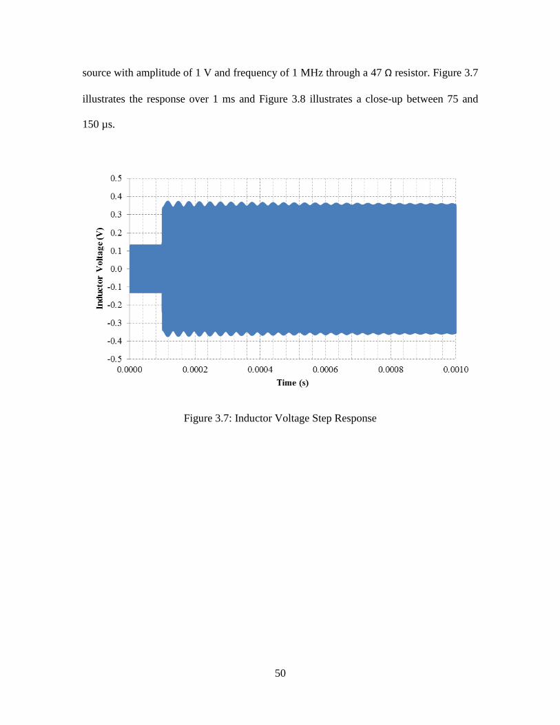
50
source with amplitude of 1 V and frequency of 1 MHz through a 47 Ω resistor. Figure 3.7
illustrates the response over 1 ms and Figure 3.8 illustrates a close-up between 75 and
150 µs.
Figure 3.7: Inductor Voltage Step Response
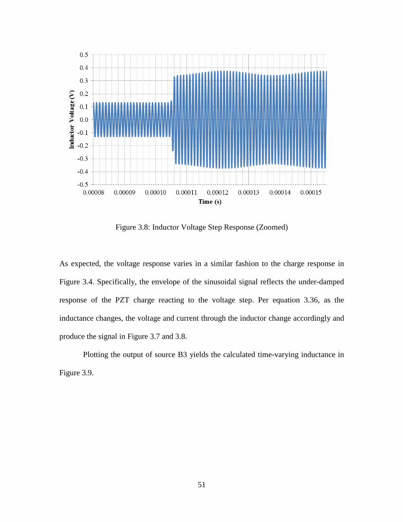
51
Figure 3.8: Inductor Voltage Step Response (Zoomed)
As expected, the voltage response varies in a similar fashion to the charge response in
Figure 3.4. Specifically, the envelope of the sinusoidal signal reflects the under-damped
response of the PZT charge reacting to the voltage step. Per equation 3.36, as the
inductance changes, the voltage and current through the inductor change accordingly and
produce the signal in Figure 3.7 and 3.8.
Plotting the output of source B3 yields the calculated time-varying inductance in
Figure 3.9.

52
Figure 3.9: Inductance Step Response
Based on the mathematics derived above and input into SPICE, the static inductance is
numerically computed and plotted over time in response to the PZT input step voltage.
This plot should be identical to that of the PZT charge response since the coupling
between PZT and Metglas was assumed to be unity. With this result, the inductance may
now indicate the tuning speed of a particular device.
3.1.4 Non-Linear Time-Variant Multiferroic Inductor
The linear time-variant assumption is valid for many inductors. However,
referring back to the B-H curves collected by Lou, et al. [3], a clear non-linear behavior is
present as magnetic field (current) is increased through the coil. At a certain field value,
the flux no longer has a linear relationship with field and the linear assumption is invalid.

53
This fact affects the previously derived measurement equations and requires further
investigation.
If magnetic flux features a non-linear relationship with current, it can be
represented generally as
Φ(t) = Φ�𝑖(𝑡), 𝜇(𝑡)� (3.47)
where 𝑖(𝑡) and 𝜇(𝑡) are functions of time. Since Faraday’s law is related to the flux rate-
of-change with respect to time, revising equation 3.1 with the new flux expression
produces
𝑣(𝑡) =𝑑Φ𝑑𝑡
=𝜕Φ𝜕𝜇
∙𝑑𝜇𝑑𝑡
+𝜕Φ𝜕𝑖
∙𝑑𝑖𝑑𝑡
(3.48)
Equation 3.48 now represents a more general case of equation 3.34 with two product
terms containing flux rate-of-change with respect to current and permeability. In equation
2.3, the dynamic inductance was introduced as the partial derivative of flux with respect
to current. Substituting into equation 3.48 yields
𝑣(𝑡) =𝜕Φ𝜕𝜇
∙𝑑𝜇𝑑𝑡
+ 𝐿𝑑(𝑡) ∙𝑑𝑖𝑑𝑡
(3.49)
Another dynamic inductance exists as a partial derivative of flux with respect to
permeability, or
𝐿𝑑𝜇(𝑡) =𝜕Φ𝜕𝜇
(3.50)
Renaming equation 2.3 results in a unique variable for dynamic inductance due to
current, or
𝐿𝑑𝑖(𝑡) =𝜕Φ𝜕𝑖
(3.51)
Substituting both into equation 3.48 produces

54
𝑣(𝑡) = 𝐿𝑑𝜇(𝑡) ∙𝑑𝜇𝑑𝑡
+ 𝐿𝑑𝑖(𝑡) ∙𝑑𝑖𝑑𝑡
(3.52)
Equation 3.52 suggests that there are at least two non-unique dynamic inductance
definitions that will require alternate methods for calculation based on measured data.
The steps taken in the previous section to determine inductance as a function of time are
useful for determining static inductance, but not dynamic.
Referring again to Figure 2.4, the trend of each B-H curve follows a hyperbolic
tangent function (the small hysteresis effect notwithstanding). This is typical behavior of
an inductor. In fact, the inductor SPICE model documentation suggests using a
hyperbolic tangent in the flux equation discussed in the previous equation [31].
Therefore,
Φ(𝑡) = tanh (𝑖(𝑡) ∙ 𝜇(𝑡)) (3.53)
is defined. By assuming a non-linear hyperbolic tangent flux, three inductance definitions
are now possible: a static inductance due to the ratio of flux to current, a dynamic
inductance due to changing current, and a dynamic inductance due to changing
permeability. These are presented using the hyperbolic tangent flux expression in
equations 3.54, 3.55, and 3.56.
𝐿𝑠(𝑡) =Φ𝑖
=tanh (𝑖 ∙ 𝜇)
𝑖 (3.54)
𝐿𝑑𝑖(𝑡) =𝜕Φ𝜕𝑖
= 𝜇 ∙ sech(𝑖 ∙ 𝜇)2 (3.55)
𝐿𝑑𝜇(𝑡) =𝜕Φ𝜕𝜇
= 𝑖 ∙ sech(𝑖 ∙ 𝜇)2 (3.56)
The flux and inductances can be plotted as functions of current and permeability to
further illustrate their complex nature.

55
Figure 3.10: Magnetic Flux vs. Current vs. Permeability
For each permeability value, the magnetic flux follows a hyperbolic tangential curve as
current is swept through its axis. An alternate two dimensional view is plotted in Figure
3.11.

56
Figure 3.11: Magnetic Flux vs. Current vs. Permeability (2D)
Figure 3.11 is similar to Figure 2.4 in chapter 2, although with more plotted curves. The
minimum and maximum permeability values correspond to the minimum and maximum
slopes of each curve. The outlines of the data plotted in Figure 3.11 suggest the relative
values of each slope at the tangent points. Note that the permeability can be extracted
from this Φ− 𝑖 curve when constant C is known, as discussed in chapter 2.
The next three figures depict the three inductances, starting with the static
inductance in Figure 3.12.
57
Figure 3.12: Static Inductance vs. Current vs. Permeability
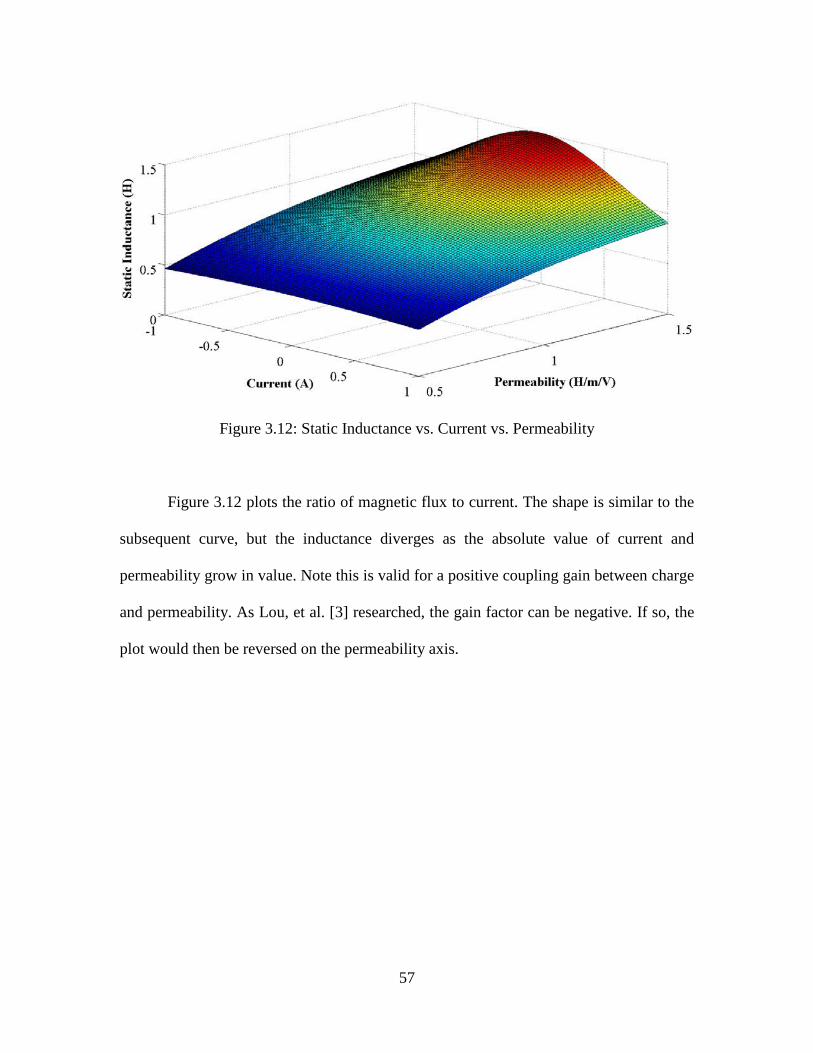
Figure 3.12 plots the ratio of magnetic flux to current. The shape is similar to the
subsequent curve, but the inductance diverges as the absolute value of current and
permeability grow in value. Note this is valid for a positive coupling gain between charge
and permeability. As Lou, et al. [3] researched, the gain factor can be negative. If so, the
plot would then be reversed on the permeability axis.

58
Figure 3.13: Dynamic Inductance (Current) vs. Current vs. Permeability
Here, the inductance tends to roll off more sharply as current is increased than in
Figure 3.12 since the inductance is a derivative with respect to current. As permeability
increases (decreases), the roll-off becomes more drastic.
59
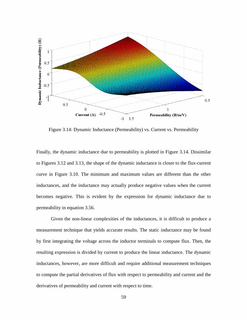
Figure 3.14: Dynamic Inductance (Permeability) vs. Current vs. Permeability
Finally, the dynamic inductance due to permeability is plotted in Figure 3.14. Dissimilar
to Figures 3.12 and 3.13, the shape of the dynamic inductance is closer to the flux-current
curve in Figure 3.10. The minimum and maximum values are different than the other
inductances, and the inductance may actually produce negative values when the current
becomes negative. This is evident by the expression for dynamic inductance due to
permeability in equation 3.56.
Given the non-linear complexities of the inductances, it is difficult to produce a
measurement technique that yields accurate results. The static inductance may be found
by first integrating the voltage across the inductor terminals to compute flux. Then, the
resulting expression is divided by current to produce the linear inductance. The dynamic
inductances, however, are more difficult and require additional measurement techniques
to compute the partial derivatives of flux with respect to permeability and current and the
derivatives of permeability and current with respect to time.

60
In any case, one is left with three inductance time-series data sets to determine the
settling time, and each will give varying results. To reduce the ambiguity, another option
is presented. A common theme among the presented methods for linear time-invariant,
linear time-variant, and non-linear time-variant is the measurement of flux via the
inductor voltage integral.
Φ− 𝐶𝐼𝑛𝑡𝑒𝑔𝑟𝑎𝑡𝑖𝑜𝑛 = � 𝑣(𝑡) ∙ 𝑑𝑡𝜏
0= �
𝑑Φ𝑑𝑡
𝜏
0∙ 𝑑𝑡 (3.57)
All of the inductance dependent variables in equation 3.57, whether linear or non-
linear, are represented by the changing flux. If the permeability is changed due to a step
voltage input to the PZT, the flux will represent the inductance transient per equation 2.3
or 2.4. Further, if current is varying through the inductor and forcing the permeability
slope to change due to non-linearity, this will also be accounted for. Although a specific
value of inductance will not be present in the measured time-series2, the tuning response
will be clearly indicated by integrating the voltage across the inductor terminals.
Additionally, since the change in permeability creates a change in flux, the flux
derivative with respect to time will also indicate the tuning response transient.
Conveniently, the flux rate-of-change has been already defined in equation 3.1 as the
voltage across the inductor terminals. When dealing with small signals that create
numerical integration errors (in an effort to compute flux), the flux rate-of-change may be
used as an alternative for determining the tuning response transient. Therefore, the flux
rate-of-change provides a rapid analytical tool that will be illustrated in chapters four and
five.
2 Methods for determining the inductance vs. PZT input voltage have been studied by Lou, et al. [3].
61
3.1.5 Non-Linear Time-Varying Multiferroic Inductor Simulation
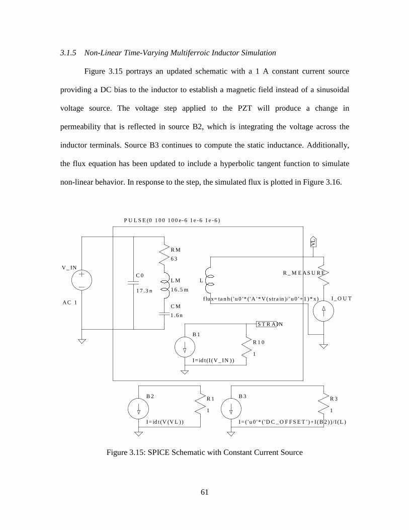
Figure 3.15 portrays an updated schematic with a 1 A constant current source
providing a DC bias to the inductor to establish a magnetic field instead of a sinusoidal
voltage source. The voltage step applied to the PZT will produce a change in
permeability that is reflected in source B2, which is integrating the voltage across the
inductor terminals. Source B3 continues to compute the static inductance. Additionally,
the flux equation has been updated to include a hyperbolic tangent function to simulate
non-linear behavior. In response to the step, the simulated flux is plotted in Figure 3.16.
Figure 3.15: SPICE Schematic with Constant Current Source
L
f lu x= ta n h ( ' u 0 '* ('A '* V (s tra in )/ ' u 0 '+ 1 )* x)1 7 .3 n
C 0
6 3R M
1 6 .5 m
L M
1 .6 nC M
A C 1
P U L S E (0 1 0 0 1 0 0 e-6 1 e -6 1 e -6 )
V _ IN
B 1
I= id t (I (V _ IN ))
R 1 0
1
R _ M E A S U R E
R 1
1
B 2
I= id t (V (V L ))
R 3
1
B 3
I= ( ' u 0 '* ( 'D C _ O F F S E T ' )+ I (B 2 ) ) /I (L )
I_ O U T
S T R A IN
VL

62
Figure 3.16: Magnetic Flux Response to Determine Tuning Speed
3.1.6 Measurement Techniques Summary
To summarize, two measurement methods are useful in generally determining the
tuning response time of a tunable inductor that features non-linear and time-varying
behavior. After providing a step voltage to the PZT, the inductor flux rate-of-change may
be measured by observing the inductor terminal voltage and
1. exciting the inductor with a sinusoidal voltage source.
2. exciting the inductor with a constant current source.
The voltage may then be integrated to compute magnetic flux and converted to static or
dynamic inductance as determined by the previous analysis with the understanding that
each inductance will result in differing values over time. If sufficient measurement
resolution is not available to perform the numerical integration required for computing
63
flux, the magnetic flux time rate-of-change is a valid substitute for determining the tuning
response time.
3.2 Actuator Electronics
To produce a sufficient input to the PZT terminals, a driving circuit is required.
Specifically, an electronic amplifier that produces hundreds of volts, provides amps of
output current, features a slew-rate of 100 V/µs, and maintains a high bandwidth is
studied to allow for microsecond switching of the PZT. The next sections discuss the
PZT load requirements, a custom amplifier design, and a commercial-off-the-shelf
(COTS) solution.
3.2.1 Load Requirements
To determine the proper specifications for the amplifier, the load must be known
so that the voltage and current requirements are explicitly defined. In support of this, an
impedance analyzer was connected to the PZT input of a multiferroic inductor and its
impedance curve generated. Figure 3.17 illustrates the magnitude and phase of tested
PZT impedance. The tested sample was obtained from a single-layer PZT sheet
manufactured by Piezo Systems that was bonded to a piece of Metglas ribbon.
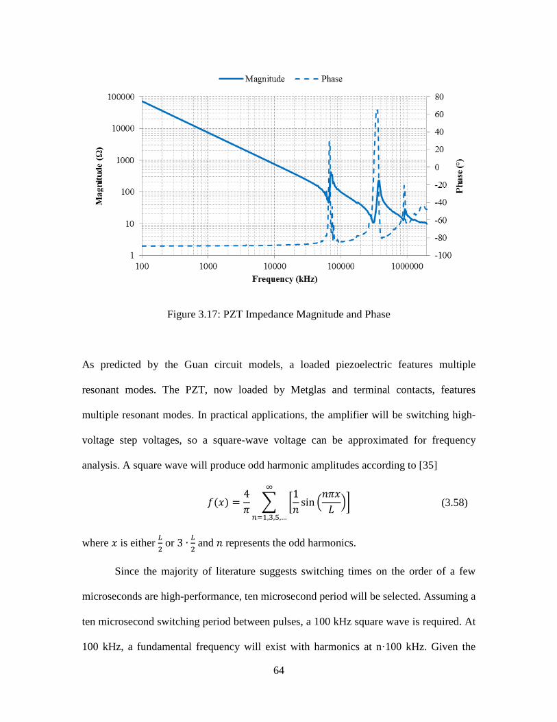
64
Figure 3.17: PZT Impedance Magnitude and Phase
As predicted by the Guan circuit models, a loaded piezoelectric features multiple
resonant modes. The PZT, now loaded by Metglas and terminal contacts, features
multiple resonant modes. In practical applications, the amplifier will be switching high-
voltage step voltages, so a square-wave voltage can be approximated for frequency
analysis. A square wave will produce odd harmonic amplitudes according to [35]
𝑓(𝑥) =4𝜋
� �1𝑛
sin �𝑛𝜋𝑥𝐿��
∞
𝑛=1,3,5,…
(3.58)
where 𝑥 is either 𝐿2 or 3 ∙ 𝐿
2 and 𝑛 represents the odd harmonics.
Since the majority of literature suggests switching times on the order of a few
microseconds are high-performance, ten microsecond period will be selected. Assuming a
ten microsecond switching period between pulses, a 100 kHz square wave is required. At
100 kHz, a fundamental frequency will exist with harmonics at n·100 kHz. Given the

65
voltage ranges published in the literature and used by Lou, et al. [3] in previous testing, a
100 V square wave is likely suitable for driving the piezoelectric and generating a
suitable tuning response. Therefore, at the fundamental frequency of 100 kHz, the
sinusoidal voltage output is
(100 𝑉) ∙4
𝜋 ∙ 𝑛= 127.3 𝑉
and drawing an impedance value from the magnitude in Figure 3.17 at 100 kHz, the
current requirement is
𝑉𝑅
=127.3 𝑉100 Ω
= 𝐼 = 1.27 𝐴
Similarly, at 300 kHz, the current requirement is
𝑉𝑅
=42.4 𝑉20 Ω
= 𝐼 = 2.12 𝐴
and at 500 kHz the value is
𝑉𝑅
=25.5 𝑉46 Ω
= 𝐼 = 0.554 𝐴
Continuing to sum the currents dictated by the remaining of the square wave harmonics
totals a maximum current of 5 A. Therefore, the amplifier may be required to produce up
to 100 V at 5 A, or 500 W of power, to an external load3. This rules out the Fleming [28]
amplifier discussed in chapter 2.
3.2.2 Custom Amplifier
Upon reviewing the literature in chapter 2, it was determined that many published
amplifiers were not suitable to produce the charge required by the PZT due to either
3 The analysis assumes ideal square-wave signals (infinite bandwidth). The amplifier naturally band-limits the square- wave, thereby reducing the amplitude of each harmonic and reducing the required current.

66
frequency or power limitations. To remedy the situation, a custom discrete amplifier was
designed. Appendix A contains a complete amplifier schematic that will be referred to
going forward.
The amplifier design features a fully differential architecture to support high-
speed current source inputs and high-voltage outputs. Beginning with the input stage, a
differential common-base stage (Q7/Q3) converts the DAC current outputs to a voltage
input while level-shifting for the next amplifier stage, similar to the ubiquitous 741 op-
amp [30]. At the input to the subsequent differential cascode stage, the signal is amplified
by the common-emitter NPN pair (Q5/Q4) and buffered by the common-base pair
(Q1/Q2). Bias is supplied by the R6/R4 resistor divider, and the 4.8 kΩ resistor pair
provides voltage gain via the currents flowing from the common-base stage. The
differential voltages are buffered by a Darlington-type configuration [36] before power
gain is supplied by the class AB output stage with paralleling for current-sharing.
Notable features include a common-mode feedback configuration to zero the
output offset voltage4 and beta-helper current mirrors. Most prominent is the lack of any
feedback compensation via the open-loop design. Without a compensation capacitor
between the first and second gain stages, high slew-rates are achievable with this
amplifier, on the order of 100 V/µs according to simulation results.
Figure 3.18 depicts a square wave voltage applied across a Guan PZT model. In
the figure, the total peak-to-peak voltage swing is 100 V at 100 kHz.
4 The common-mode feedback amplifier is represented by an ideal DC servo amplifier in the Appendix A schematic [37].
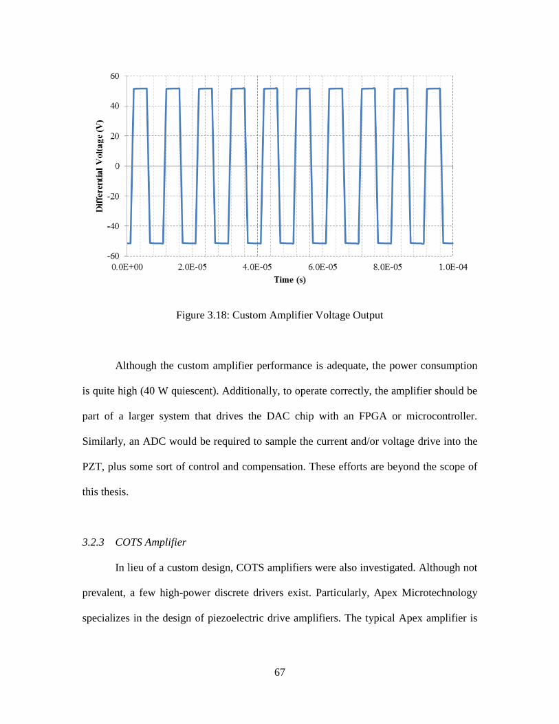
67
Figure 3.18: Custom Amplifier Voltage Output
Although the custom amplifier performance is adequate, the power consumption
is quite high (40 W quiescent). Additionally, to operate correctly, the amplifier should be
part of a larger system that drives the DAC chip with an FPGA or microcontroller.
Similarly, an ADC would be required to sample the current and/or voltage drive into the
PZT, plus some sort of control and compensation. These efforts are beyond the scope of
this thesis.
3.2.3 COTS Amplifier
In lieu of a custom design, COTS amplifiers were also investigated. Although not
prevalent, a few high-power discrete drivers exist. Particularly, Apex Microtechnology
specializes in the design of piezoelectric drive amplifiers. The typical Apex amplifier is

68
capable of supplying hundreds of volts with many amps of current while supporting high
frequency outputs in the kHz region.
To support the 500 W power delivery and 100 V/µs slew-rate requirement, the
Apex Microtechnology MP111 was selected. The MP111 performance features are
highlighted in table 3.1.
Table 3.1: Apex Microtechnology MP111 Amplifier Specifications
Parameter Value
Peak-to-Peak Voltage ~90 V
Current Output (Pulse) 50 A
Current Output (Continuous) 15 A
Slew Rate 130 V/µs
Power Bandwidth 500 kHz
Gain Bandwidth Product 6 MHz
Power Supply ±50 V
Power (Quiescent) 16 W
Notable specifications are the large output currents and high power bandwidth, or the
highest supportable bandwidth while delivering a full voltage swing to the desired load.
Additionally, the MP111 requires less power than the custom design.

69
Figure 3.19: Apex Microtechnology MP111 Equivalent Schematic [39]
For completeness, the equivalent circuit schematic is shown in Figure 3.19. The
MP111 is a hybrid class AB design comprised of junction field effect transistors (JFET),
bipolar junction transistors (BJT), and metal oxide semiconductor field effect transistors
(MOSFET). Similar to the custom design, the input stage is a JFET/MOSFET cascode
configuration followed by a PMOS common-source amplifier. The class AB output stage
is biased by BJT transistors while power MOSFETs handle delivering current to the load.
The compensation capacitor is external to the circuit and parallels the second gain stage.

70
3.2.4 Amplifier Implementation
Given the two amplifier options, the COTS amplifier was selected as the PZT
driver as it featured acceptable specifications compared to the custom amplifier,
including high-voltage, fast slew-rate, high bandwidth, and large current output.
Although pursuing the custom option may have led to increased performance, the COTS
specifications are suitable to provide a step input voltage and supply the necessary charge
to the PZT. Additionally, the MP111 was readily available and was priced well for the
purposes of this research. The following paragraphs discuss the methods required to
prepare the MP111 for integration into the test system.
The assembly of the Apex Microtechnology MP111 was facilitated by the
purchase of the EV57 evaluation kit. The kit features a large and small heat sink, a
printed circuit board (PCB) for power and signal routing, high-power interface
connectors, power supply bypass capacitors, and a user area for soldering feedback
resistors and a compensation capacitor. Without the EV57, integration of the amplifier
into the measurement system would prove difficult.
Figure 3.20 on the following page shows the MP111 amplifier and EV57
evaluation kit side-by-side. Power, ground, and the amplifier output are connected to the
black terminal strip at the bottom of the board as indicated in Figure 3.20. The user-
modifiable area is also depicted.
When assembled, the amplifier sits beneath the tall black heat sink located in the
center of the green PCB in Figure 3.20. Further below the amplifier is a larger heat sink
that conducts heat away from the sensitive discrete components on the amplifier PCB.
Figure 3.21 illustrates this more clearly on the following page.
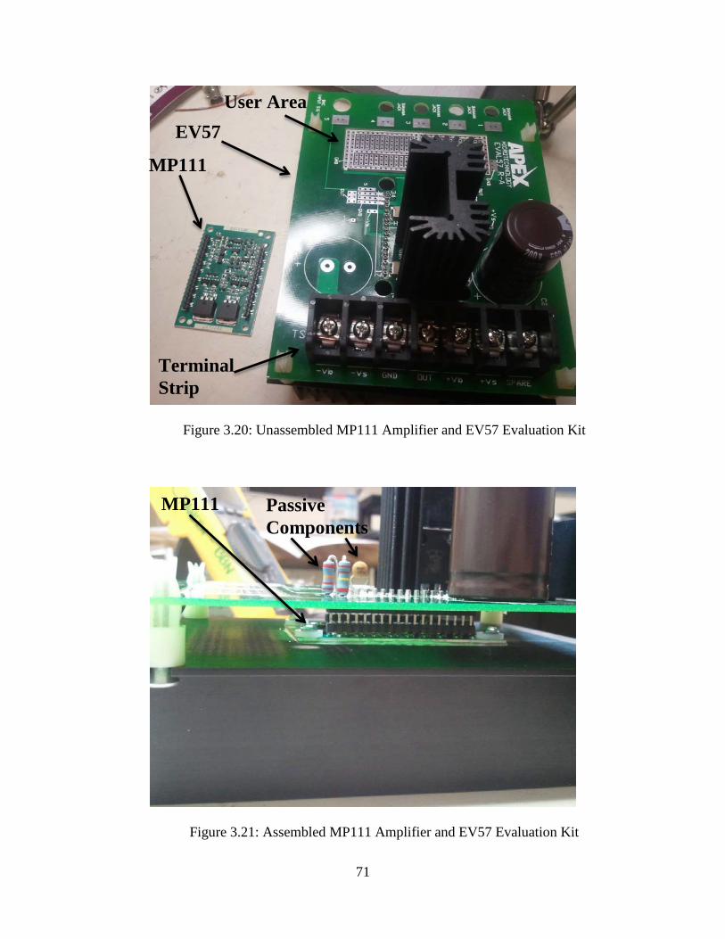
71
Figure 3.20: Unassembled MP111 Amplifier and EV57 Evaluation Kit
Figure 3.21: Assembled MP111 Amplifier and EV57 Evaluation Kit
MP111
EV57
MP111
User Area
Terminal Strip
Passive Components
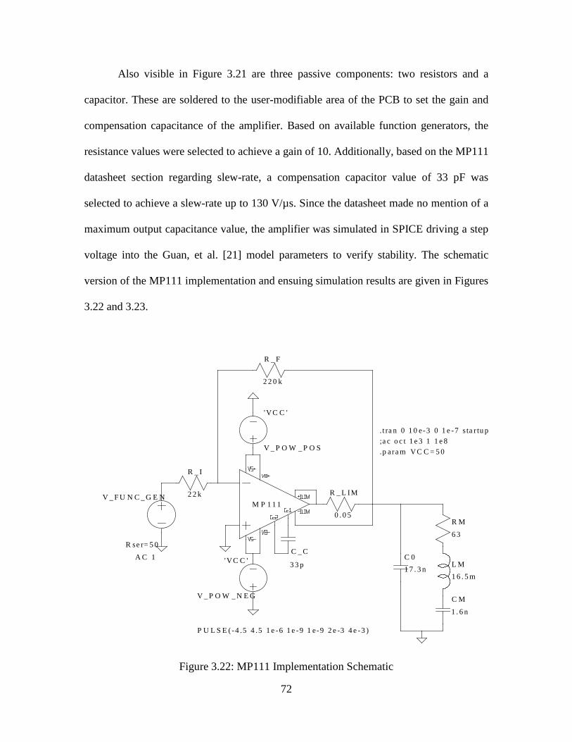
72
Also visible in Figure 3.21 are three passive components: two resistors and a
capacitor. These are soldered to the user-modifiable area of the PCB to set the gain and
compensation capacitance of the amplifier. Based on available function generators, the
resistance values were selected to achieve a gain of 10. Additionally, based on the MP111
datasheet section regarding slew-rate, a compensation capacitor value of 33 pF was
selected to achieve a slew-rate up to 130 V/µs. Since the datasheet made no mention of a
maximum output capacitance value, the amplifier was simulated in SPICE driving a step
voltage into the Guan, et al. [21] model parameters to verify stability. The schematic
version of the MP111 implementation and ensuing simulation results are given in Figures
3.22 and 3.23.
Figure 3.22: MP111 Implementation Schematic
M P 1 1 1
C _ C
3 3 p
R _ L IM
0 . 0 5
R _ F
2 2 0 k
R _ I
2 2 k
V _ P O W _ P O S
'V C C '
A C 1
R se r= 5 0
P U L S E (-4 .5 4 .5 1 e -6 1 e -9 1 e-9 2 e -3 4 e -3 )
V _ F U N C _ G E N
V _ P O W _ N E G
'V C C '1 7 . 3 nC 0
6 3
R M
1 6 . 5 mL M
1 . 6 n
C M
.t ra n 0 1 0 e-3 0 1 e -7 s ta r tu p
.p ara m V C C = 5 0;a c o c t 1 e 3 1 1 e 8
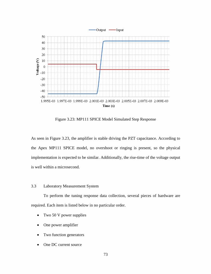
73
Figure 3.23: MP111 SPICE Model Simulated Step Response
As seen in Figure 3.23, the amplifier is stable driving the PZT capacitance. According to
the Apex MP111 SPICE model, no overshoot or ringing is present, so the physical
implementation is expected to be similar. Additionally, the rise-time of the voltage output
is well within a microsecond.
3.3 Laboratory Measurement System
To perform the tuning response data collection, several pieces of hardware are
required. Each item is listed below in no particular order.
• Two 50 V power supplies
• One power amplifier
• Two function generators
• One DC current source
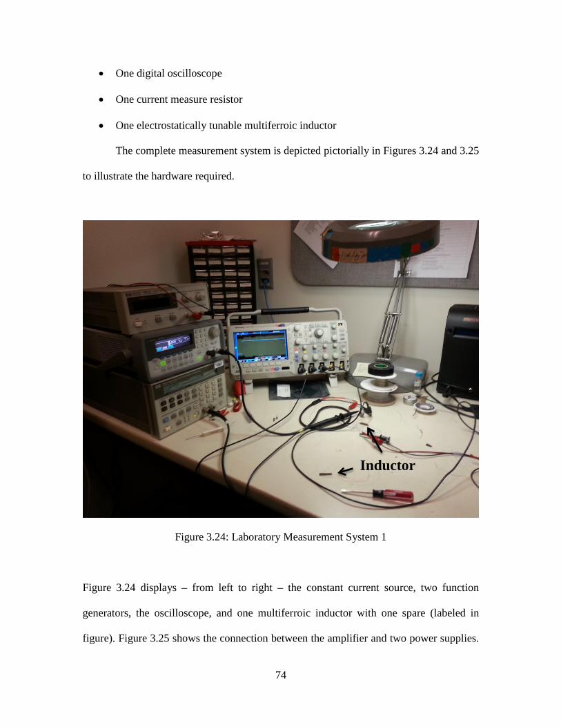
74
• One digital oscilloscope
• One current measure resistor
• One electrostatically tunable multiferroic inductor
The complete measurement system is depicted pictorially in Figures 3.24 and 3.25
to illustrate the hardware required.
Figure 3.24: Laboratory Measurement System 1
Figure 3.24 displays – from left to right – the constant current source, two function
generators, the oscilloscope, and one multiferroic inductor with one spare (labeled in
figure). Figure 3.25 shows the connection between the amplifier and two power supplies.
Inductor

75
Two isolated, dual-channel 25 V supplies were each stacked in series to form one +50
and one -50 V supply. Then, the supplies were connected across the power amplifier as
discussed in the COTS amplifier implementation section.
Figure 3.25: Laboratory Measurement System 2
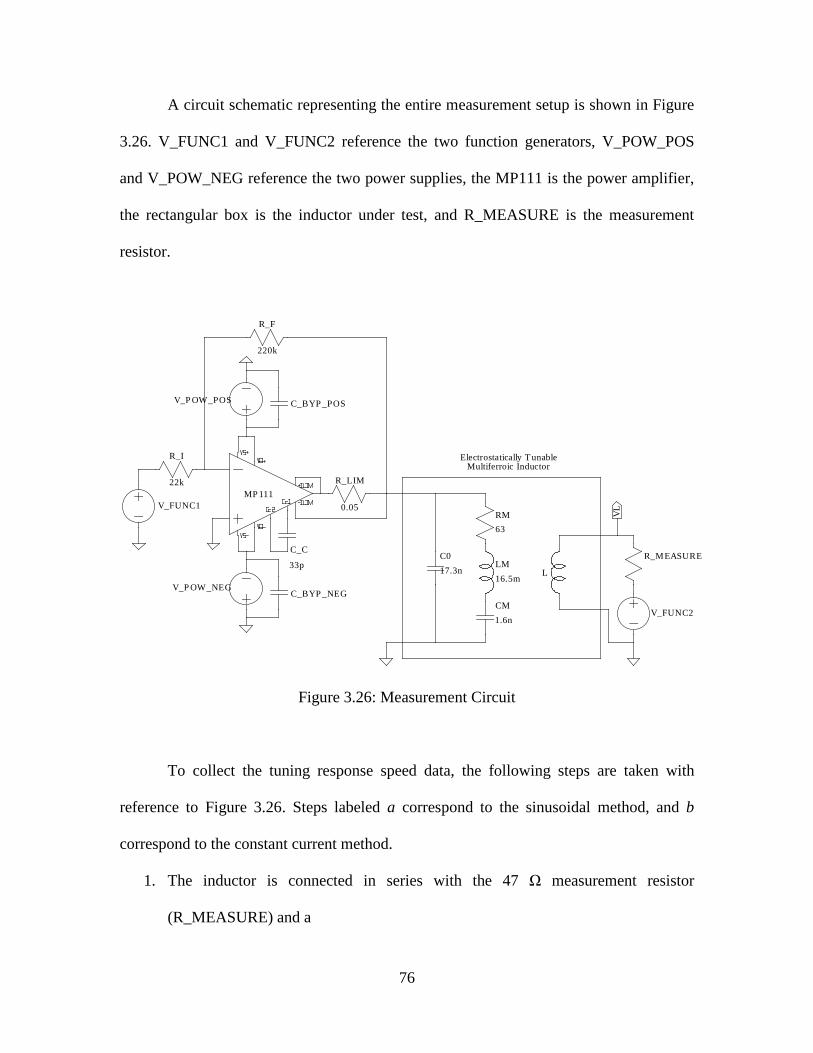
76
A circuit schematic representing the entire measurement setup is shown in Figure
3.26. V_FUNC1 and V_FUNC2 reference the two function generators, V_POW_POS
and V_POW_NEG reference the two power supplies, the MP111 is the power amplifier,
the rectangular box is the inductor under test, and R_MEASURE is the measurement
resistor.
Figure 3.26: Measurement Circuit
To collect the tuning response speed data, the following steps are taken with
reference to Figure 3.26. Steps labeled a correspond to the sinusoidal method, and b
correspond to the constant current method.
1. The inductor is connected in series with the 47 Ω measurement resistor
(R_MEASURE) and a
MP 111
C_C
33p
R_LIM
0.05
R_F
220k
R_I
22k
V_P OW_POS
V_P OW_NEG
V_FUNC1
L17.3nC0
63RM
16.5mLM
1.6nCM
R_MEASURE
V_FUNC2
C_BYP _NEG
C_BYP _POS
VL
Electrostatically T unableMultiferroic Inductor

77
a. function generator.
b. DC constant current source.
2. An oscilloscope is connected across the VL node.
3. The power amplifier is connected to the PZT control input.
4. The two power supplies are connected to the +Vs and -Vs inputs of the power
amplifier.
5. A second function generator is connected to the input of the power amplifier.
6. Power is applied to each device.
7. The inductor driving source is set to
a. drive a 1 V sinusoidal signal at 5 MHz into the resistor-inductor
combination
b. drive a 100 mA constant current through the resistor-inductor combination
8. The second function generator is set to drive a 4.5 V square wave at 0.5 Hz into
the power amplifier (to achieve a 90 V peak-to-peak output voltage into the PZT).
9. The oscilloscope is set to trigger on the power amplifier voltage output and the
voltage at VL is recorded by the oscilloscope.
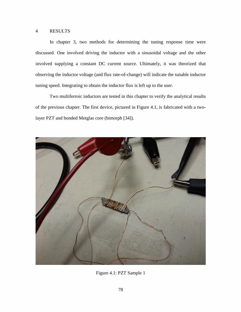
78
4 RESULTS
In chapter 3, two methods for determining the tuning response time were
discussed. One involved driving the inductor with a sinusoidal voltage and the other
involved supplying a constant DC current source. Ultimately, it was theorized that
observing the inductor voltage (and flux rate-of-change) will indicate the tunable inductor
tuning speed. Integrating to obtain the inductor flux is left up to the user.
Two multiferroic inductors are tested in this chapter to verify the analytical results
of the previous chapter. The first device, pictured in Figure 4.1, is fabricated with a two-
layer PZT and bonded Metglas core (bimorph [34]).
Figure 4.1: PZT Sample 1

79
The second is comprised of a single PZT sheet bonded to a Metglas core. The
device is pictured in Figure 4.2 (damaged due to overheating).
Figure 4.2: PZT Sample 2
Results obtained from both the sinusoidal and constant current methods are
illustrated, as well as additional measured data to attempt further insight into the tuning
speed dynamics.
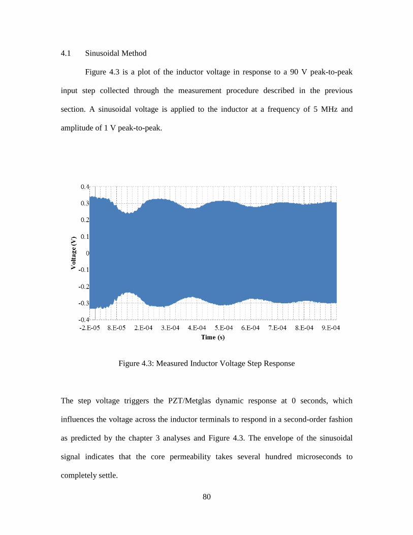
80
4.1 Sinusoidal Method
Figure 4.3 is a plot of the inductor voltage in response to a 90 V peak-to-peak
input step collected through the measurement procedure described in the previous
section. A sinusoidal voltage is applied to the inductor at a frequency of 5 MHz and
amplitude of 1 V peak-to-peak.
Figure 4.3: Measured Inductor Voltage Step Response
The step voltage triggers the PZT/Metglas dynamic response at 0 seconds, which
influences the voltage across the inductor terminals to respond in a second-order fashion
as predicted by the chapter 3 analyses and Figure 4.3. The envelope of the sinusoidal
signal indicates that the core permeability takes several hundred microseconds to
completely settle.

81
To confirm the inductor tuning response, the current flow into the PZT is plotted
in Figure 4.4. Although noisy, the general waveform is clear.
Figure 4.4: Measured PZT Current Response
The plot shows a current peak of approximately one ampere that decays over a period of
roughly 300 µs before dropping into the noise floor.
Another interesting response is the sinusoidal voltage response to a step voltage
applied to the PZT with opposite polarity. This data is presented in Figure 4.5.

82
Figure 4.5: Measured Inductor Voltage Step Response (Reverse Polarity)
Although the inductor has clearly changed its inductance as indicated by the voltage
envelope, the response is not quite the same as in Figure 4.3. Reversing the polarity of the
step input has some effect on the inductor’s tuning response. In this case, the tuning
speed has increased by a few hundred microseconds. Figure 4.6 shows the current flow
into the PZT for the reverse polarity step voltage.
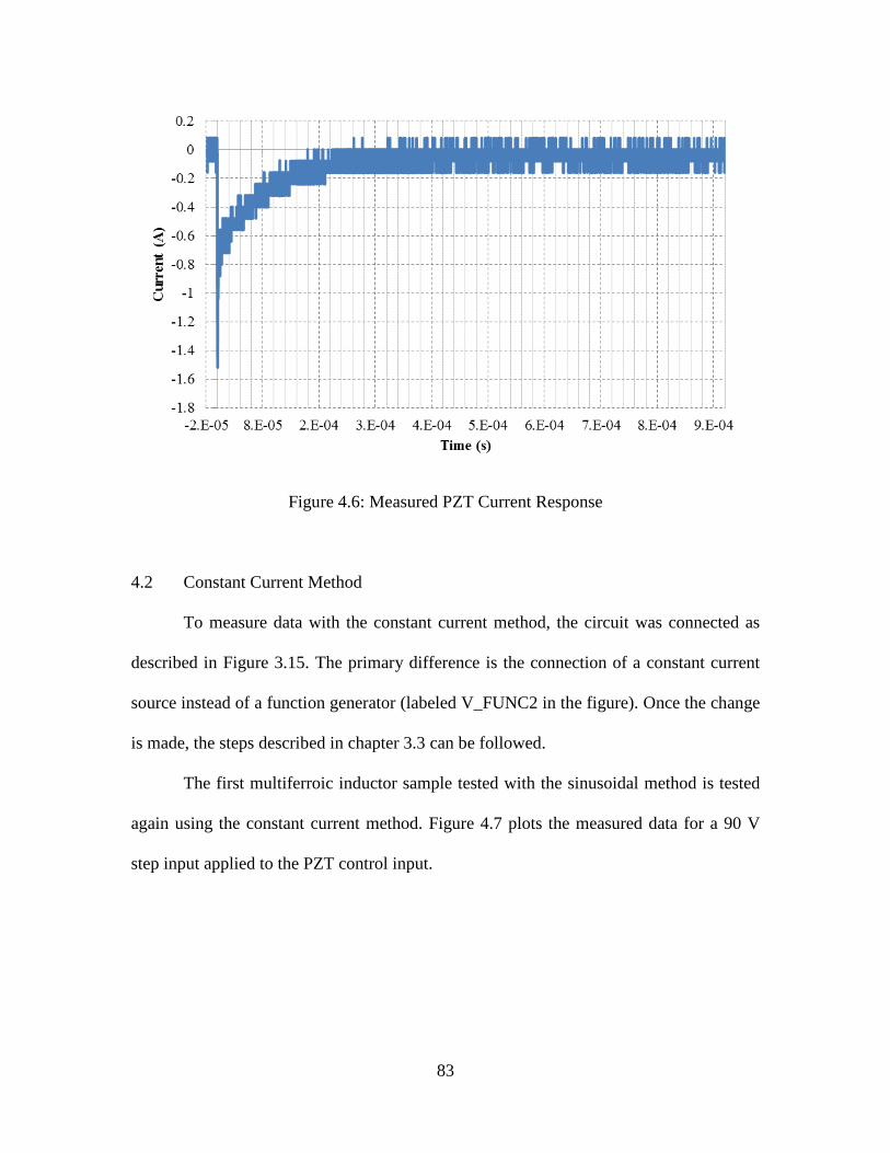
83
Figure 4.6: Measured PZT Current Response
4.2 Constant Current Method
To measure data with the constant current method, the circuit was connected as
described in Figure 3.15. The primary difference is the connection of a constant current
source instead of a function generator (labeled V_FUNC2 in the figure). Once the change
is made, the steps described in chapter 3.3 can be followed.
The first multiferroic inductor sample tested with the sinusoidal method is tested
again using the constant current method. Figure 4.7 plots the measured data for a 90 V
step input applied to the PZT control input.
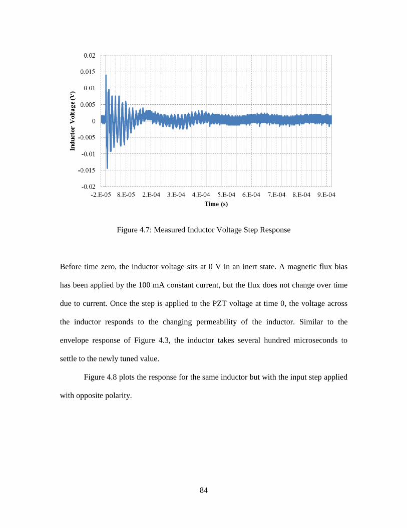
84
Figure 4.7: Measured Inductor Voltage Step Response
Before time zero, the inductor voltage sits at 0 V in an inert state. A magnetic flux bias
has been applied by the 100 mA constant current, but the flux does not change over time
due to current. Once the step is applied to the PZT voltage at time 0, the voltage across
the inductor responds to the changing permeability of the inductor. Similar to the
envelope response of Figure 4.3, the inductor takes several hundred microseconds to
settle to the newly tuned value.
Figure 4.8 plots the response for the same inductor but with the input step applied
with opposite polarity.
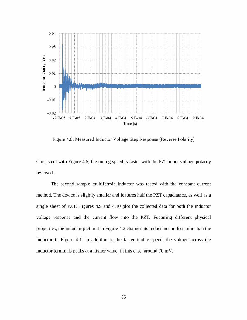
85
Figure 4.8: Measured Inductor Voltage Step Response (Reverse Polarity)
Consistent with Figure 4.5, the tuning speed is faster with the PZT input voltage polarity
reversed.
The second sample multiferroic inductor was tested with the constant current
method. The device is slightly smaller and features half the PZT capacitance, as well as a
single sheet of PZT. Figures 4.9 and 4.10 plot the collected data for both the inductor
voltage response and the current flow into the PZT. Featuring different physical
properties, the inductor pictured in Figure 4.2 changes its inductance in less time than the
inductor in Figure 4.1. In addition to the faster tuning speed, the voltage across the
inductor terminals peaks at a higher value; in this case, around 70 mV.
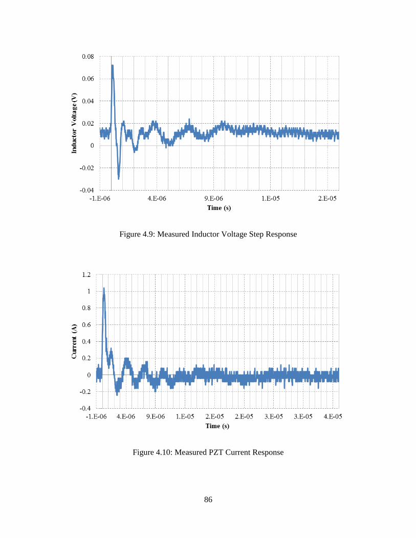
86
Figure 4.9: Measured Inductor Voltage Step Response
Figure 4.10: Measured PZT Current Response

87
5 DISCUSSION
The following section discusses the measured results obtained from experimental
methods conceived in the previous chapter. Specifically, the tuning response data for two
sample electrostatically tunable multiferroic inductors comprised of a PZT/Metglas core
and 26 AWG coil are discussed. Improvements to the work presented in this thesis are
also recommended.
5.1 Tuning Speed
The first tested device achieved a tuning speed on the order of several hundred
microseconds as shown in Figures 4.3 and 4.7. The results are improved over the data
collected by Chen, et al. [18], as the slow reported tuning speed can be attributed to the
reduced slew-rate and current capacity of the power amplifier referenced. In any case, the
tuning speed is still slower than desired; however, as another research group [20] has
seen multiferroic switching speed on the order of a few microseconds. The discrepancy
can be attributed to the physical properties of the devices tested as a second tunable
inductor achieved tuning speed on the order of several microseconds (Figure 4.9).
As discussed, the first tested device was constructed of with two-layers of PZT
sheets, forming a bimorph bending-type device. These devices are noted for their reduced
resonances over single-layer PZT sheets [34]. Generally speaking, open-loop PZT can
typically achieve nominal displacement in approximately 1/3 of the lowest resonant mode
period, or
𝑡0 ≈1
3 ∙ 𝑓0 (5.1)
88
albeit with strong overshoot [34]. With resonances in the low kHz region, this implies
settling times of tens to hundreds of microseconds (or more) for PZT bimorph devices.
These estimates are consistent with the measured results in Figures 4.3 and 4.7 for tested
two-layer device.
According to the PZT impedance plot in 3.17, the single-layer PZT has a low
resonant mode near 60 kHz, implying a nominal tuning speed of
13∙
160000
≈ 5.6 𝜇𝑠
According to Figure 4.9, the tuning response is beginning to decay rapidly after
approximately 5 µs which corresponds nicely to the nominal speed predicated by
equation 5.1.
Regarding the response of Figure 4.5, one possible explanation for the increased
tuning speed is the saturation point of the Metglas ribbons [3]. Once the negative step
voltage is applied, the permeability may be saturating and causing a decrease in the
change in inductance with respect to time. Referring to Figure 2.4, the permeability is
noted to decrease as applied voltage is increased. Further, the range of available
permeability values is large before saturation occurs. However, as negative (reverse
polarity) voltage is applied, the data is not depicted. It is possible that the permeability
range available in the negative voltage direction is not as large. In other words, given the
permeability of the device with 0 V applied, the range of permeability values may not be
symmetric for positive and negative applied voltages. This would suggest that the
permeability offset in equation 3.43 has a negative skew and is close to the saturation
region. Therefore, the behavior could be a possible non-linear effect.

89
Generally, as discussed by Chen, et al. [18], the Metglas response time is on the
order of one microsecond, so the majority of the lower frequency dynamics are
contributed by the PZT. If a PZT is proven to achieve switching speed in the low
microsecond range, a multiferroic inductor using that same PZT will likely achieve
similar tuning speed based on analysis presented in this document. The experimental data
contributes to this idea as well, as both current response in Figures 4.4 and 4.10 mimic
their inductor tuning response settling times.
5.2 Measurement Techniques
In chapter 4, two measurement techniques were used on the sample multiferroic
tunable inductors. The first involved driving a sinusoidal voltage into a series a resistor-
inductor combination and examining the envelope of the sinusoid across the tunable
inductor terminals as it is affected by changing inductance. The second method required a
constant current source that sets up a magnetic bias in the inductor. Then, when a step
voltage is applied to the PZT, the voltage at the inductor terminals reflects the changing
inductance via changing magnetic flux.
As a result of the experiments, the constant current method is preferred. The
principal reason is the resolution at which the dynamics of the PZT/Meglas core can be
visualized. For example, Figure 4.7 not only displays the lower frequency resonant mode
described by the voltage envelope in Figure 4.3, but a second resonance is seen at a
higher frequency. This second resonance was expected as a result of the load
characterization in Figure 3.17, but the sinusoidal measurement technique obscures the
resonance as seen in Figure 4.3. Further, the constant current method requires a simpler
90
setup. The measurement resistor in Figure 3.15 is not required for the test, and only a DC
source capable of providing a constant current is necessary.
One drawback with the constant current method is the required resolution of the
measurement system. Collecting data with a standard digital oscilloscope limits the
precision to the selected voltage range which, in the case of Figures 4.7 and 4.8, is
approximately 0.4 mV 5. Evident in the aforementioned figures is the lower resonant
mode (which is clearly visible in Figure 4.3) falling below the noise floor. Performing
any sort of numerical integration to compute magnetic flux or static/dynamic inductances
over time proves difficult due to the noisy data.
Theoretically, however, the constant current method is expected to produce lower
measurement voltages. This can be illustrated by a Laplace domain representation of
equation 3.52. When a constant current is applied to the multiferroic inductor, equation
3.52 for dynamic inductance simplifies to
𝑣𝐿(𝑡) = 𝐿𝑑𝜇(𝑡) ∙𝑑𝜇𝑑𝑡
+ 𝐿𝑑𝑖(𝑡) ∙ 0 = 𝐿𝑑𝜇(𝑡) ∙𝑑𝜇𝑑𝑡
(5.2)
Performing a Laplace transform yields
𝑉𝐿(𝑠) = 𝐿𝑑𝜇(𝑠) ∙ 𝑠 ∙ 𝑀𝑀𝑒𝑡𝑔𝑙𝑎𝑠(𝑠) (5.3)
assuming no initial conditions. Dividing by the Laplace-domain permeability expression
produces
𝑉𝐿(𝑠)
𝑀𝑀𝑒𝑡𝑔𝑙𝑎𝑠(𝑠)= 𝑠 ∙ 𝐿𝑑𝜇(𝑠) (5.4)
and in the frequency domain
5 80 mV/ 8 bits of resolution = 0.3125 mV

91
𝑉𝐿(𝜔)
𝑀𝑀𝑒𝑡𝑔𝑙𝑎𝑠(𝜔)= 𝑗 ∙ 𝜔 ∙ 𝐿𝑑𝜇(𝜔) (5.5)
The expression in equation 5.5 is analogous to the frequency domain representation of
LTI inductor impedance. For this application, equation 5.5 states that the output voltage,
VL, will have its amplitude dictated by the frequency of the driving source, or the Metglas
permeability. Larger frequencies will produce larger changes in the dynamic inductance,
and this will be represented by larger voltages. Since the Metglas frequency domain
response is dictated by the PZT, the frequencies in which equation 5.5 is subjected to are
typically less than 100 kHz as evidenced by Figure 2.7.
In the sinusoidal case, changes in inductance can be amplified by an order of
magnitude over the constant current method. This is evident by the frequency-domain
impedance expression for inductor impedance [8], or
𝑉𝐿(𝜔)𝐼𝐿(𝜔)
= 𝑗 ∙ 𝜔 ∙ 𝐿 (5.6)
If 𝐼𝐿 is a sinusoidal current source operating at 𝜔, any changes in 𝐿 will be gained by a
factor dependent on the frequency and be reproduced in the voltage across the inductor
terminals. In summary, the constant current method will typically produce smaller
amplitude voltages across the inductor terminals due the frequency of the driving source,
or the PZT/Metglas dynamic response.
To remedy the quality of the data collected and make the gain factor of equation
5.6 a moot point, a high-impedance instrumentation amplifier can be used across the
inductor rather than an oscilloscope. The amplifier offers the added benefit of reduced
input capacitance over the oscilloscope probes (which are upward of 130 pF). The
resulting data will feature a much lower noise floor and be more conducive to numerical

92
processing. In other words, the tuning speed may converted to units of magnetic flux,
static inductance, or dynamic inductance.
5.3 Future Work
To continue the research in this thesis, the methods for characterizing the tuning
speed of a multiferroic inductor should be applied to a large quantity of devices and
verified against traditional piezoelectric and Metglas characterization methods. The
quality of measurement should be improved through the use of instrumentation amplifiers
and sensitive measurement devices. Further, the fabrication of the multiferroic tunable
inductors will hopefully improve over time, thus leading to consistent measured data for
comparison.
To integrate this work into applied systems research, investigation must be done
into the control of the PZT/Metglas dynamic response. Driving step voltages to achieve
fast tuning speed causes the PZT to respond with overshoot, ringing, and prolonged
settling time. Many methods of control exist and are beyond the scope of this thesis.
However, a proposed block level diagram is presented in Figure 5.1 as a starting point.
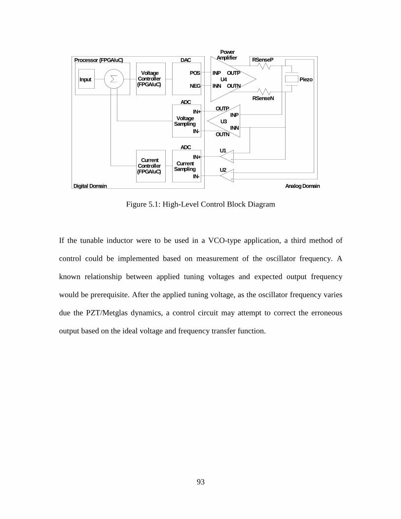
93
Figure 5.1: High-Level Control Block Diagram
If the tunable inductor were to be used in a VCO-type application, a third method of
control could be implemented based on measurement of the oscillator frequency. A
known relationship between applied tuning voltages and expected output frequency
would be prerequisite. After the applied tuning voltage, as the oscillator frequency varies
due the PZT/Metglas dynamics, a control circuit may attempt to correct the erroneous
output based on the ideal voltage and frequency transfer function.
RSenseP
RSenseN
U1
U2
POS
NEG
INP
INN
OUTP
OUTN
DACProcessor (FPGA/uC)
IN+
IN-
Input Piezo
IN+
IN-
VoltageSampling
CurrentSampling
ADC
ADC
Digital Domain
PowerAmplifier
CurrentController(FPGA/uC)
VoltageController(FPGA/uC)
INP
INN
OUTP
OUTN
U3
Analog Domain
U4
94
6 CONCLUSION
A study on the transient analysis of an electrostatically tunable multiferroic
inductor has been presented. Throughout the discussion, the inductor’s importance to
current high-speed applications was established through a review of the state of current
research, a developed methodology for determining the tuning response speed,
experimental data collected in the laboratory, and a discussion highlighting the concerns
with the presented work. In doing so, the electrostatically tunable inductor was shown to
be suitable for integration into RF applications. Although the tuning speed is device
dependent, multiferroic inductors can be fabricated that approach tuning speeds on the
order of just a few microseconds, rivaling competing technologies such as RF MEMS
tunable inductors [4][6][9][11].
As the fabrication of electrostatically tunable inductors continues to improve, the
tuning speeds should continue to increase, further establishing the inductor as a leading
technology for RF applications. The work presented here can potentially contribute to the
continued research, design, and development of novel tunable devices.

95
7 REFERENCES
[1] C.-W. Nan, M. Bichurin, D. Shuxiang, D. Viehland, G. Srinivasan,
“Multiferroic magnetoelectric composites: Historical perspective, status, and
future directions,” J. of Appl. Physics, vol. 103, no. 3, pp. 031101-35, Feb. 2008.
[2] A. Tatarenko, V. Gheevarughese, G. Srinivasan, “Magnetoelectric microwave
bandpass filter,” IEEE Electron. Lett., vol. 42, no. 9, pp. 540-541, Apr. 2006.
[3] J. Lou, D. Reed, M. Liu, N. Sun, “Electrostatically tunable inductors with
multiferroic composites,” Appl. Physics Lett., vol. 94, no. 11, pp. 112508, Mar.
2009.
[4] G. Rebeiz, K. Entesari, I. Reines, S.-J. Park, M. El-Tanani, A. Grichener, A.
Brown, “Tuning in to RF MEMS,” IEEE Microwave, vol. 10, no. 6, pp. 55-
72, Oct. 2009.
[5] J. Kim, J. Choi, K.-H. Lee, F. Bien, K. Lim, C.-H. Lee, “Wideband CMOS
voltage-controlled oscillator using tunable inductors,” IEEE Electron. Lett., vol.
46, no. 20, pp. 1391-1393, Sep. 2010.
[6] C. Pavageau, O. Millet, A. Cao, “An approach of rf-mems technology platform
for multi-band multi-mode handsets,” DelfMEMS, Villeneuve-d'Ascq, France,
2011.
[7] A. Hussaini, R. Abd-Alhameed, J. Rodriguez, “Tunable RF filters: Survey and
beyond,” in 2011 18th IEEE Int. Conf. on Electron., Circuits and Systems
(ICECS), pp. 512-515, Dec. 2011.
96
[8] J. Nilsson, S. Riedel, Electric Circuits, 5th ed. Reading, MA: Addison-
Wesley, 2004.
[9] S. Yonghyun, W. Zhengzheng, M. Rais-Zadeh, “A high-performance
continuously tunable MEMS bandpass filter at 1 GHz,” IEEE Trans. Microw.
Theory Tech., vol. 60, no. 8, pp. 2439-2447, Aug. 2012.
[10] C. Leifso, J. Haslett, “A fully integrated active inductor with independent voltage
tunable inductance and series-loss resistance,” IEEE Trans. Microw. Theory
Tech., vol. 49, no. 4, pp. 671-676, Apr. 2001.
[11] G. Rebeiz, RF MEMS: Theory, Design, and Technology. Hoboken, NJ: J. Wiley,
2003.
[12] N. Sun and G. Srinivasan, “Voltage control of magnetism in multiferroic
heterostructures and devices,” SPIN, vol. 02, pp. 1240004, 2012.
[13] T. Carroll, M. Todd, F. Rachford, L. Pecora, “Spatiotemporal nonlinear dynamics
of a magnetoelastic ribbon”, Phys. Rev. E Stat. Nonlin. Soft Matter Phys., vol. 63,
no. 5 pt. 2, pp. 056205, 2001.
[14] IEEE standard on piezoelectricity, ANSI/IEEE Standard 176-1987, 1988.
[15] J. Kraus, and D. Fleisch, “Dielectric and magnetic materials,” in
Electromagnetics with Applications. 5th ed. Boston, MA: WCB/McGraw-Hill,
1999, ch. 7, 441-442.
[16] F. Hyde, D. Tucker, “Parametric amplifiers: Static and dynamic inductance
and capacitance and their significance in the non-linear and time-varying
approaches,” IEEE Radio and Electronic Engineer, vol. 25, no. 4, pp. 353-355,
Apr. 1963.
97
[17] Y. Chen, A. Geiler, T. Fitchorov, C. Vittoria, V. Harris, “Time domain
analyses of the converse magnetoelectric effect in a multiferroic metallic glass-
relaxor ferroelectric heterostructure,” Appl. Physics Lett., vol. 95, no. 18, pp.
182501-3, Nov. 2009.
[18] Y. Chen, T. Fitchorov, A. Geiler, J. Gao, C. Vittoria, V. Harris, ”Dynamic
response of converse magnetoelectric effect in a PMN-PT-based multiferroic
heterostructure,” Appl. Physics A, vol. 100, no. 4, pp. 1149-1155, 2010.
[19] A. Ustinov and G. Srinivasan, “Speed of a ferrite-ferroelectric microwave planar
resonator,” Tech. Physics, vol. 55, no. 6, pp. 900-903, 2010.
[20] A. Ustinov, Y. Fetisov, S. Lebedev, G. Srinivasan, “Electric switching in
bistable ferrite-piezoelectric microwave resonator,” Tech. Physics Lett., vol. 36,
no. 2, pp. 166-169, 2010.
[21] M. Guan, W.-H. Liao, “Studies on the circuit models of piezoelectric ceramics,”
Int. Conf. on Information Acquisition, 2004. Proc., pp. 26- 31, Jun. 2004.
[22] S. Robinson, “Driving piezoelectric actuators,” Power Electron. Tech., pp. 40-44,
Apr. 2006.
[23] L. Jin, X. Yao, X. Wei, Z. Xi, “Observation of piezoelectric resonance in time
domain transient current of ferroelectric ceramics and crystals,” Appl. Physics
Lett., vol. 87, no. 7, pp. 072910-3, Aug. 2005.
[24] D. Biolek, Z. Kolka, V. Biolkova, “Modeling time-varying storage components in
PSpice,” Dept. of EE, FMT, University of Defence Brno, Dept. of
Microelectronics/Radioelectronics, FEEC, Brno University of Technology, Brno,
Czech Republic, 2007.
98
[25] G. Lewis, W. Olbricht, “Design and characterization of a high-power
ultrasound driver with ultralow-output impedance,” Review of Scientific
Instruments, vol. 80, no. 11, pp. 114704-8, Nov. 2009.
[26] J. Borg, J. Johansson, “An ultrasonic transducer interface IC with integrated push-
pull 40 Vpp, 400 mA current output, 8-bit DAC and integrated HV multiplexer,”
IEEE J. Solid-State Circuits, vol. 46, no. 2, pp. 475-484, Feb. 2011.
[27] C. Wallenhauer, B. Gottlieb, R. Zeichfusl, A. Kappel, “Efficiency-improved
high-voltage analog power amplifier for driving piezoelectric actuators,” IEEE
Trans. Circuits Syst. I, Reg. Papers, vol. 57, no. 1, pp. 291-298, Jan. 2010.
[28] A. Fleming, “A megahertz bandwidth dual amplifier for driving piezoelectric
actuators and other highly capacitive loads,” Review of Scientific Instruments, vol.
80, no. 10, pp. 104701-7, Oct. 2009.
[29] M. Colclough, “A fast high-voltage amplifier for driving piezoelectric
positioners Review of Scientific Instruments, vol. 71, no. 11, pp. 4323-4324, Nov.
2000.
[30] P. Gray, P. Hurst, S. Lewis, R. Meyer, Analysis and design of analog
integrated circuits. 4th ed. New York: Wiley, 2001.
[31] LTspice software manual, Linear Technology Corporation, Milpitas, CA, 2013.
Available: http://ltspice.linear.com/software/LTspiceIV.exe
[32] J. Phillips, “Piezoelectric technology primer,” CTS Wireless Components,
Albuquerque, NM, 2000.
[33] G. Franklin, J. Powell, A. Emami-Naeini, Feedback control of dynamic
systems, 5th ed. Upper Saddle River, NJ: Pearson, 2005.
99
[34] Piezoelectric actuators: Components, technologies, operation. Physik
Instrumente Ceramic, Lederhose, Germany, 2012.
[35] E. Weisstein. Square wave [Online].
Available: http://mathworld.wolfram.com/SquareWave.html
[36] A. Sedra and K. Smith, Microelectronic circuits, 5th ed. New York: Oxford
University Press, 2003.
[37] B. Cordell, Designing audio power amplifiers, 1st ed. New York, NY: McGraw-
Hill, 2011.
[38] A. Safari and E. Akdogan, Piezoelectric and acoustic materials for transducer
applications. Springer, 2008.
[39] MP111 power operational amplifier, MP111U REVF, Apex Microtechnology,
Tucson, AZ, 2012.

100
APPENDIX A (Custom amplifier schematic on following page)

101
Figure A.1: Custom Amplifier Design Schematic
V1
50
V2
-50
V3
1
I1
PULSE(1e-3 7e-3 1e-6 1e-6 1e-6 4e-6 10e-6)
R5
100
V4
-1
R3
200k
R8
50
R9
4.8kI2
PULSE(7e-3 1e-3 1e-6 1e-6 1e-6 4e-6 10e-6)
R1
200k
R2
100
R7
50
R10
4.8k Cm1
1.6e-9
Lm1
16.5e-3
Rm1
63
Rp1
7.5e6
Co1
17.3e-9
Rs1
40R4
14k
R6
100k
R11
200
C1
12p
C2
12p
I84e-3
AC 3e-3
I94e-3
AC -3e-3
R12
2.35k
R13
1.25k
Q3
PNP
Q7
PNP
Q33
PNP
Q34
PNP
Q10
PNP
Q14
PNP
Q16
PNP
Q24
NPN
Q25
NPN
Q1
NPN
Q2
NPN
Q4
NPN
Q5
NPN
Q23
NPN
Q26
NPN
Q27
NPN
Q28
NPN
Q29
NPN
Q6
PNP
Q9
PNP
Q30
NPN
Q32
NPN
Q11
NPN
Q12
NPN
Q13
NPN
Q15
NPN
Q17
NPN
Q18
PNP
Q20
PNP
Q22
PNP
Q31
PNP
Q35
PNP
Q8
NPN
Q19
NPN
Q21
NPN
R14
10k
R15
10k
E11e6
C3
1µ
R19
1e6
Q36
NPN
Q37
NPN
VCC
VEE
VD
ACL
IM-
VD
ACL
IM+
VD
ACL
IM+
VCC
VD
ACL
IM-
VEE
VCC
OU
T-
VEE
OU
T+
VEE
VCC
VCC
VCC
VEE
VCC
VEE
VCC
VEE
VEE
VEE
npnMirrorBase
VEE
VCC
VCC
inputOUT-inputOUT+
inputOUT-inputOUT+
VEE
VCC
VCC
VCC
VEE
VCC
VEE
VCC
VEE
VEE
VEE
VEE
npnMirrorBasenpnMirrorBase
npnMirrorBase
npnMirrorBase
npnMirrorBase
pnpMirrorBase
pnpMirrorBase
pnpMirrorBase
VCC
OUTCM
VCC
VCC
OU
TCM
.tran 0 1000e-6 0 1e-6
;ac oct 1e3 1 1e9
TI DAC900 producing 100 kHz differential square wave
Current Mirrors
Sources