Embed Size (px)
Citation preview

Sun Microsystems, Inc.4150 Network CircleSanta Clara, CA 95054 U.S.A.650-960-1300
Send comments about this document to: [email protected]
Netra™ CP2140 TechnicalReference and Installation Manual
Part No. 816-4908-10October 2002, Revision A

Copyright 2002 Sun Microsystems, Inc., 4150 Network Circle, Santa Clara, California 95054, U.S.A. All rights reserved.
Sun Microsystems, Inc. has intellectual property rights relating to technology embodied in the product that is described in this document. Inparticular, and without limitation, these intellectual property rights may include one or more of the U.S. patents listed athttp://www.sun.com/patents and one or more additional patents or pending patent applications in the U.S. and in other countries.
This document and the product to which it pertains are distributed under licenses restricting their use, copying, distribution, anddecompilation. No part of the product or of this document may be reproduced in any form by any means without prior written authorization ofSun and its licensors, if any.
Third-party software, including font technology, is copyrighted and licensed from Sun suppliers.
Parts of the product may be derived from Berkeley BSD systems, licensed from the University of California. UNIX is a registered trademark inthe U.S. and in other countries, exclusively licensed through X/Open Company, Ltd.
Sun, Sun Microsystems, the Sun logo, AnswerBook2, docs.sun.com, Netra, UltraSPARC, OpenBoot, SunVTS, SolsticeDiskSuite, and Solaris aretrademarks or registered trademarks of Sun Microsystems, Inc. in the U.S. and in other countries.
All SPARC trademarks are used under license and are trademarks or registered trademarks of SPARC International, Inc. in the U.S. and in othercountries. Products bearing SPARC trademarks are based upon an architecture developed by Sun Microsystems, Inc.
The OPEN LOOK and Sun™ Graphical User Interface was developed by Sun Microsystems, Inc. for its users and licensees. Sun acknowledgesthe pioneering efforts of Xerox in researching and developing the concept of visual or graphical user interfaces for the computer industry. Sunholds a non-exclusive license from Xerox to the Xerox Graphical User Interface, which license also covers Sun’s licensees who implement OPENLOOK GUIs and otherwise comply with Sun’s written license agreements.
Use, duplication, or disclosure by the U.S. Government is subject to restrictions set forth in the Sun Microsystems, Inc. license agreements and asprovided in DFARS 227.7202-1(a) and 227.7202-3(a) (1995), DFARS 252.227-7013(c)(1)(ii) (Oct. 1998), FAR 12.212(a) (1995), FAR 52.227-19, orFAR 52.227-14 (ALT III), as applicable.
DOCUMENTATION IS PROVIDED "AS IS" AND ALL EXPRESS OR IMPLIED CONDITIONS, REPRESENTATIONS AND WARRANTIES,INCLUDING ANY IMPLIED WARRANTY OF MERCHANTABILITY, FITNESS FOR A PARTICULAR PURPOSE OR NON-INFRINGEMENT,ARE DISCLAIMED, EXCEPT TO THE EXTENT THAT SUCH DISCLAIMERS ARE HELD TO BE LEGALLY INVALID.
Copyright 2002 Sun Microsystems, Inc., 4150 Network Circle, Santa Clara, California 95054, Etats-Unis. Tous droits réservés.
Sun Microsystems, Inc. a les droits de propriété intellectuels relatants à la technologie incorporée dans le produit qui est décrit dans cedocument. En particulier, et sans la limitation, ces droits de propriété intellectuels peuvent inclure un ou plus des brevets américains énumérésà http://www.sun.com/patents et un ou les brevets plus supplémentaires ou les applications de brevet en attente dans les Etats-Unis et dansles autres pays.
Ce produit ou document est protégé par un copyright et distribué avec des licences qui en restreignent l’utilisation, la copie, la distribution, et ladécompilation. Aucune partie de ce produit ou document ne peut être reproduite sous aucune forme, parquelque moyen que ce soit, sansl’autorisation préalable et écrite de Sun et de ses bailleurs de licence, s’il y ena.
Le logiciel détenu par des tiers, et qui comprend la technologie relative aux polices de caractères, est protégé par un copyright et licencié par desfournisseurs de Sun.
Des parties de ce produit pourront être dérivées des systèmes Berkeley BSD licenciés par l’Université de Californie. UNIX est une marquedéposée aux Etats-Unis et dans d’autres pays et licenciée exclusivement par X/Open Company, Ltd.
Sun, Sun Microsystems, le logo Sun, AnswerBook2, docs.sun.com, Netra, UltraSPARC, OpenBoot, SunVTS, SolsticeDiskSuite et Solaris sont desmarques de fabrique ou des marques déposées de Sun Microsystems, Inc. aux Etats-Unis et dans d’autres pays.
Toutes les marques SPARC sont utilisées sous licence et sont des marques de fabrique ou des marques déposées de SPARC International, Inc.aux Etats-Unis et dans d’autres pays. Les produits protant les marques SPARC sont basés sur une architecture développée par SunMicrosystems, Inc.
L’interface d’utilisation graphique OPEN LOOK et Sun™ a été développée par Sun Microsystems, Inc. pour ses utilisateurs et licenciés. Sunreconnaît les efforts de pionniers de Xerox pour la recherche et le développment du concept des interfaces d’utilisation visuelle ou graphiquepour l’industrie de l’informatique. Sun détient une license non exclusive do Xerox sur l’interface d’utilisation graphique Xerox, cette licencecouvrant également les licenciées de Sun qui mettent en place l’interface d ’utilisation graphique OPEN LOOK et qui en outre se conformentaux licences écrites de Sun.
LA DOCUMENTATION EST FOURNIE "EN L’ÉTAT" ET TOUTES AUTRES CONDITIONS, DECLARATIONS ET GARANTIES EXPRESSESOU TACITES SONT FORMELLEMENT EXCLUES, DANS LA MESURE AUTORISEE PAR LA LOI APPLICABLE, Y COMPRIS NOTAMMENTTOUTE GARANTIE IMPLICITE RELATIVE A LA QUALITE MARCHANDE, A L’APTITUDE A UNE UTILISATION PARTICULIERE OU AL’ABSENCE DE CONTREFAÇON.
Contents
Contents 3
Figures 11
Tables 15
Code Samples 19
Safety Agency Compliance Statements 21
Regulatory Compliance Statements 25
Declaration of Conformity 29
Declaration of Conformity 30
Preface 31
Who Should Use This Book 31
How This Book Is Organized 32
Related References 32
Sun Microsystems Publications 33
Reference Documents 34
Typographic Conventions 35
3
Shell Prompts 35
Accessing Sun Documentation Online 36
Sun Welcomes Your Comments 36
1. Introduction 1–1
1.1 Netra CP2140 Board System Configuration 1–4
1.2 Features of Netra CP2140 Board CompactPCI Host Board 1–5
1.3 Hot-Swap Support 1–7
1.4 Front Panel I/O Connectors and Indicators 1–8
1.5 Software Requirements 1–9
1.6 Determining Netra CP2140 Board Identification Numbers 1–10
1.6.1 Netra CP2140 Board Assembly Identification 1–10
1.6.2 Determining Firmware Versions 1–12
1.6.3 Determining Software Version 1–12
1.7 Technical Support and Warranty 1–12
2. Installation 2–1
2.1 System Configurations 2–1
2.2 Orderable Items 2–3
2.3 Preinstallation Checklist 2–6
2.3.1 System Checklist 2–7
2.3.2 Viewing Web Pages and Reading Documents 2–8
2.3.3 Power Budgeting 2–8
2.3.4 Getting the Latest OpenBoot PROM Version 2–8
2.3.5 Completing Space, Network, and Environmental Planning 2–9
2.3.6 Determine Local Network IP Addresses and Host Names 2–9
2.4 Safety 2–10
2.5 Installation Procedure Summary 2–10
2.6 Materials and Tools Required 2–11
4 Netra CP2140 Technical Reference and Installation Manual • October 2002
2.7 Configuring the Netra CP2140 Board Hardware 2–12
2.7.1 Installing Memory Modules 2–12
2.7.2 PMC Module Installation 2–14
2.8 Configuring Transition Card Hardware 2–16
2.8.1 Installing PIM Assemblies 2–16
2.8.2 Replacing the Serial EEPROM 2–16
2.9 Installing the XCP2040-TRN I/O Transition Card 2–18
2.10 Installing the Netra CP2140 Board 2–18
2.11 Connecting Cables to the Netra CP2140 Board 2–22
2.11.1 Powering on Your System With External SCSI Peripherals 2–23
2.12 Hot-Swapping the Netra CP2140 Board 2–23
2.12.1 Basic Hot-Swapping 2–24
2.12.2 Full Hot-Swapping 2–25
2.13 Connecting Devices to a XCP2040-TRN I/O Transition Card 2–27
2.13.1 Adding CompactPCI Cards and Drivers to a Netra CP2140 BoardSystem 2–28
2.13.1.1 To Install a CompactPCI Card 2–28
2.13.1.2 To Verify That the Board is Recognized by the System2–28
2.13.1.3 To Obtain Additional Assistance 2–29
2.13.2 Backplane and Cardcage Considerations 2–29
2.14 Initial Power-On and Firmware Update 2–29
2.15 Software Installation 2–30
2.16 Setting Up a Network 2–31
2.17 Standalone Operation 2–32
3. Netra CP2140 Board Specifications 3–1
3.1 Board Features and Specifications 3–1
3.1.1 CPU 3–2
3.1.2 Main Memory 3–3
Contents 5

3.1.3 PCI Mezzanine Module (PMC) Interface 3–4
3.1.3.1 Estimated Power Requirements 3–4
3.1.4 Mechanical 3–5
3.1.5 Environmental Specifications 3–5
3.1.6 Reliability and Availability 3–6
3.1.7 Compliance 3–6
3.1.8 Safety 3–7
4. Hardware Description 4–1
4.1 Physical 4–1
4.2 Summary Description 4–3
5. Functional Description 5–1
5.1 Functional Blocks 5–2
5.1.1 UltraSPARC IIi Processor 5–2
5.1.2 SDRAM Memory 5–2
5.1.3 Firmware 5–3
5.1.3.1 System (Boot) Flash Memory 5–3
5.1.3.2 User Flash Memory 5–3
5.1.3.3 NVRAM 5–3
5.1.3.4 Serial I2C EEPROM 5–3
5.2 Clock Frequencies 5–4
5.3 Bus Subsystems 5–4
5.3.1 APB PCI Bus Interfaces 5–5
5.3.2 PCIO-2 A and PCIO-2 B Devices and EBus Paths 5–5
5.3.3 CompactPCI Bus 5–6
5.3.4 System I/O 5–7
5.3.5 PMC and PIM Interface 5–8
5.3.6 System Management Controller 5–9
6 Netra CP2140 Technical Reference and Installation Manual • October 2002
5.3.7 Watchdog Timer 5–11
5.4 Reset and Interrupts 5–11
5.4.1 CPU Reset 5–12
5.4.1.1 Power On 5–12
5.4.1.2 Power Off 5–12
5.4.2 Reset Modes 5–12
5.5 Power Subsystem 5–15
5.5.1 Power Module 5–16
5.5.2 Early Power and IPMI Power 5–16
5.6 Hot Swap 5–17
5.7 Programmable Logic Device (PLD)/Arbiter 5–18
6. Firmware 6–1
6.1 Initialization Firmware 6–1
6.1.1 Firmware CORE and BPOST 6–2
6.1.2 CPOST and EPOST 6–4
6.1.3 OpenBootPROM 6–4
6.1.4 Example of a show-devs Device Tree 6–5
6.1.5 Example of devalias Command 6–7
6.2 Firmware NVRAM Variables 6–9
6.2.1 Firmware CORE NVRAM Variables 6–9
6.2.2 Firmware CORE Execution Control 6–9
6.2.3 OpenBoot PROM Configuration Variables 6–10
6.3 Firmware Memory Map 6–13
6.4 Firmware CORE Features 6–15
6.5 ASM Support 6–16
6.6 Determining Firmware Version 6–18
6.6.1 From OpenBoot PROM 6–18
6.6.2 If Running Solaris Software 6–18
Contents 7

6.7 OpenBoot PROM Flash Update 6–19
6.7.0.1 Accessing SMC Config Block 6–19
6.7.0.2 Using Flash Update Commands 6–20
6.7.0.3 Field CORE/OpenBoot PROM Firmware Upgrade 6–21
6.7.0.4 Sequence to Boot Up the Correct OpenBoot PROMImage 6–22
6.7.1 SMC Firmware Update 6–24
6.7.2 IPMI Packet 6–24
6.8 Host-to-Host Communication 6–31
6.8.1 Packet 6–32
6.8.2 Event Receiver 6–33
6.8.3 Protocol 6–33
6.8.4 Generating an Event From SPARC to Send to Another SPARC 6–34
6.9 SMC Implementation Note 6–35
6.10 Firmware Diagnostics 6–38
6.10.1 Setting Diagnostic Levels 6–39
6.10.2 Basic POST (BPOST) 6–39
6.10.3 Comprehensive POST (CPOST) 6–40
6.10.4 Extended POST 6–40
6.10.5 OpenBoot PROM Onboard Diagnostics 6–42
6.10.6 OpenBoot Diagnostics 6–42
A. Connector Pinouts and Switch Settings A–1
A.1 CompactPCI Connectors A–1
A.1.1 Mini Din 8-Pin Connector A–17
A.1.2 RJ45 Connector A–17
A.1.3 PMC Connectors A–18
A.1.4 PMC J3002 Connector A–21
8 Netra CP2140 Technical Reference and Installation Manual • October 2002

A.1.5 PMC J3003 Connector A–22
A.2 Memory Module Connector Pinout A–25
A.3 SMC Switch Settings for HA and Non-HA Systems A–27
A.3.1 Setting Non-HA Systems A–27
A.3.2 Setting HA Systems A–28
A.4 SCSI and Flash Switch Settings A–29
A.4.1 Flash Device Selection Switches A–29
A.4.2 SCSI Termination Switches A–30
B. Mechanical Drawings B–1
C. SunVTS C–1
D. Solaris Sun FRU ID 1–3
D.1 Prtfru Command 1–3
Glossary Glossary–7
Index Index–13
Contents 9

10 Netra CP2140 Technical Reference and Installation Manual • October 2002

Figures
FIGURE 1-1 Netra CP2140 Board (Without Heat Sink) 1–2
FIGURE 1-2 Typical Netra CP2140 Board System Host or Satellite Host Board 1–3
FIGURE 1-3 Non-redundant Netra CP2140 Board HA Configuration - One System Host Board 1–4
FIGURE 1-4 Netra CP2140 I/O Front Panel 1–9
FIGURE 1-5 Location of Netra CP2140 Board Identification Labels 1–11
FIGURE 2-1 Examples of Netra CP2140 Board Hardware Configurations 2–2
FIGURE 2-2 Netra CP2140 Board Major Components and Connectors 2–5
FIGURE 2-3 XCP2040-TRN Transition Card Connectors 2–6
FIGURE 2-4 Single- and Double-wide Memory Modules 2–13
FIGURE 2-5 A Typical Netra CP2140 Board with Memory Modules Installed 2–14
FIGURE 2-6 Installing the PCI Mezzanine Card 2–15
FIGURE 2-7 Replacing the Serial I2C EEPROM 2–17
FIGURE 2-8 Netra CP2140 Board System Interface: One System Controller Board, One Satellite Board,Two Transition Cards 2–20
FIGURE 2-9 Netra CP2140 Board Installation (Close-up View) 2–21
FIGURE 2-10 Releasing and Locking the Netra CP2140 Board Injector/Ejector Handles 2–26
FIGURE 4-1 Netra CP2140 Board with Heat sink, SMC, Power Module and SDRAM Module 4–2
FIGURE 4-2 Solder Side of the Netra CP2140 Board 4–3
FIGURE 4-3 Netra CP2140 Board Functional Block Diagram 4–4
FIGURE 5-1 Netra CP2140 Board Detailed Block Diagram 5–1
FIGURE 5-2 UltraSPARC IIi Interface 5–2
11

FIGURE 5-3 Netra CP2140 Board PCI Bus Interface 5–5
FIGURE 5-4 CompactPCI Bus Interface 5–6
FIGURE 5-5 Netra CP2140 Board I/O Interface 5–7
FIGURE 5-6 PCI Mezzanine Module Interface on Host Board 5–9
FIGURE 5-7 System Management Controller Interface 5–10
FIGURE 5-8 Simplified Reset Paths 5–14
FIGURE 5-9 Power Distribution Block Diagram 5–15
FIGURE 5-10 Selection Between Early Power and IPMI Power 5–17
FIGURE 6-1 Control Flow from Power On for Firmware CORE and Client Modules—Solaris Case 6–2
FIGURE 6-2 System Flash PROM Map 6–14
FIGURE 6-3 Host-to-Host Communication 6–31
FIGURE 6-4 Basic POST Services 6–39
FIGURE 6-5 POST Enables OEMs to add Diagnostics 6–41
FIGURE A-1 Netra CP2140 Board Connectors A–2
FIGURE A-2 J1 Connector A–3
FIGURE A-3 Netra CP2140 Board J2 Connector A–6
FIGURE A-4 Netra CP2140 Board J3 Connector A–8
FIGURE A-5 Netra CP2140 Board J4/P4 Connector A–10
FIGURE A-6 Netra CP2140 Board J5/P5 Connector A–13
FIGURE A-7 Serial Connector- Mini Din 8-Pin Front Panel TTYA Diagram A–17
FIGURE A-8 RJ45 Ethernet Connector Diagram A–17
FIGURE A-9 J3001-J3003 Connectors A–19
FIGURE A-10 Memory Module Connectors J0601 and J0602 A–24
FIGURE A-11 Setting Switches to Closed Position A–27
FIGURE A-12 SW0501 Position for non-HA Systems A–28
FIGURE A-13 Location of SW0501 on SMC Module A–28
FIGURE A-14 SW0501 Switch Setting for HA Systems A–29
FIGURE A-15 Switch Setting Legend A–29
FIGURE A-16 SCSI Termination Switch Setting Example A–30
FIGURE A-17 SCSI Switch Selections and SMC on the Netra CP2140 Board A–32
12 Netra CP2140 Technical Reference and Installation Manual • October 2002

FIGURE B-1 Mechanical Drawing of the Netra CP2140 Board Front Panel B–2
FIGURE B-2 Mechanical Dimensions of the Netra CP2140 Board B–3
FIGURE B-3 Netra CP2140 Board Mechanical Dimensions of the Heat sink and Single-wide MemoryModule B–4
FIGURE B-4 Netra CP2140 Board Mechanical Dimensions of the Heat sink and Double-wide MemoryModule B–5
Figures 13

14 Netra CP2140 Technical Reference and Installation Manual • October 2002

Tables
TABLE 1-1 Netra CP2140 Board Features 1–5
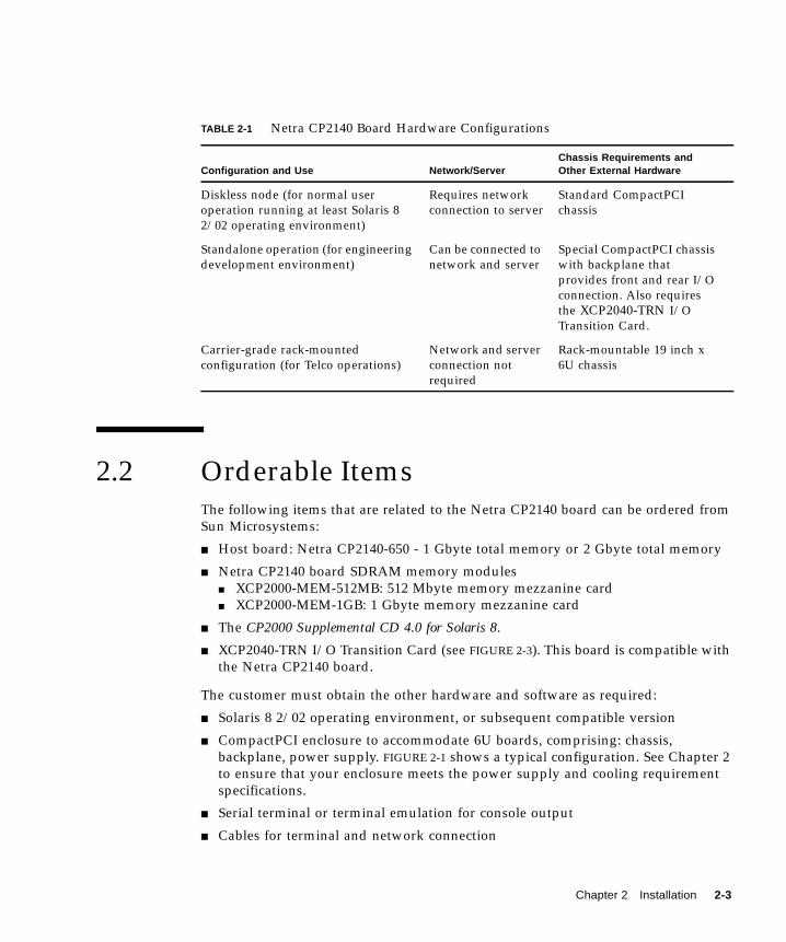
TABLE 2-1 Netra CP2140 Board Hardware Configurations 2–3
TABLE 2-2 Preinstallation Checklist 2–7
TABLE 2-3 Netra CP2140 Board I/O Hardware Configurations 2–12
TABLE 3-1 Netra CP2140 Board Physical Dimensions 3–1
TABLE 3-2 System Compatibility Attributes 3–2
TABLE 3-3 CompactPCI Bus Interface 3–2
TABLE 3-4 CPU Specification 3–2
TABLE 3-5 Memory Specification 3–3
TABLE 3-6 Netra CP2140 Board Memory Module Configurations 3–3
TABLE 3-7 PMC Interface Specification 3–4
TABLE 3-8 Estimated Power Dissipation for the Netra CP2140 Board 3–4
TABLE 3-9 Environmental Conditions and Limits 3–5
TABLE 3-10 Reliability Prediction for Board Level MTBF 3–6
TABLE 5-1 Clock Frequencies 5–4
TABLE 5-2 Host-SMC Commands 5–11
TABLE 5-3 Available Reset Operating Modes 5–13
TABLE 6-1 Firmware CORE and BPOST Flow of Execution 6–3
TABLE 6-2 Firmware Execution Control Key Sequences 6–9
TABLE 6-3 NVRAM Configuration Variables 6–10
15
TABLE 6-4 OpenBoot PROM Environment Variable Settings for Executing the POST Modules 6–12
TABLE 6-5 Firmware CORE Monitor Commands 6–15
TABLE 6-6 Chassis Configuration Example 6–28
TABLE 6-7 IPMI Packet 6–29
TABLE A-1 J1/P1 Connector Pin Assignments A–3
TABLE A-2 Signal Definitions A–4
TABLE A-3 J2/P2 Connector Pin Assignments A–6
TABLE A-4 Signal Definitions A–7
TABLE A-5 J3/P3 Connector Pin Assignments A–9
TABLE A-6 Signal Definitions A–9
TABLE A-7 J4/P4 Connector Pin Assignments A–10
TABLE A-8 Signal Definitions A–11
TABLE A-9 MII Signals A–12
TABLE A-10 SCSI single-ended levels - SCSI-A on J4 and SCSI-B on J5 A–12
TABLE A-11 J5/P5 Connector Pin Assignments A–14
TABLE A-12 Miscellaneous A–15
TABLE A-13 USB Signals A–15
TABLE A-14 Parallel Port A–15
TABLE A-15 Serial COM Ports (A and B), RS 232 Levels A–15
TABLE A-16 Floppy Disk Drive, TTL Levels A–16
TABLE A-17 Keyboard/Auxiliary Device Signals A–16
TABLE A-18 Serial Mini Din 8-pin Connector Pinouts A–17
TABLE A-19 Netra CP2140 Board Front Panel Ethernet Connector Pinout A–18
TABLE A-20 PMC J3001 Connector Pinouts A–19
TABLE A-21 PMC J3002 Connector Pinouts A–21
TABLE A-22 PMC J3003 Connector Pinouts A–22
TABLE A-23 Memory Module Connector 1 Pinout (Bottom Side) A–25
TABLE A-24 Memory Module Connector 2 Pinout (Bottom Side) A–26
TABLE A-25 Flash Device Switch Setting (SW1801) A–30
TABLE A-26 SCSI Termination Switch Setting (SW2401) A–31
16 Netra CP2140 Technical Reference and Installation Manual • October 2002

TABLE D-1 Description of Fields in Typical Prtfru Command Display Output 1–4
Tables 17

18 Netra CP2140 Technical Reference and Installation Manual • October 2002

Code Samples
CODE EXAMPLE 6-1 show-devs Command Output 6-5
CODE EXAMPLE 6-2 devalias Command Output 6-7
CODE EXAMPLE 6-3 EBus Packet for Command 0xf6 6-34
CODE EXAMPLE 6-4 Response Packet for EBus Command 0xf6 6-34
19

20 Netra CP2140 Technical Reference and Installation Manual • October 2002
Safety Agency ComplianceStatementsRead this section before beginning any procedure. Thefollowing text provides safety precautions to follow wheninstalling a Sun Microsystems product.
Safety PrecautionsFor your protection, observe the following safetyprecautions when setting up your equipment:
■ Follow all cautions and instructions marked on theequipment.
■ Ensure that the voltage and frequency of your powersource match the voltage and frequency inscribed onthe equipment’s electrical rating label.
■ Never push objects of any kind through openings inthe equipment. Dangerous voltages may be present.Conductive foreign objects could produce a shortcircuit that could cause fire, electric shock, or damageto your equipment.
SymbolsThe following symbols may appear in this book:
Caution – There is a risk of personal injuryand equipment damage. Follow theinstructions.
Caution – Hot surface. Avoid contact.Surfaces are hot and may cause personalinjury if touched.
Caution – Hazardous voltages are present. Toreduce the risk of electric shock and danger topersonal health, follow the instructions.
On – Applies AC power to the system.
Depending on the type of power switch your device has,one of the following symbols may be used:
Off – Removes AC power from the system.
Standby – The On/Standby switch is in thestandby position.
Modifications to EquipmentDo not make mechanical or electrical modifications to theequipment. Sun Microsystems is not responsible forregulatory compliance of a modified Sun product.
Placement of a Sun Product
Caution – Do not block or cover the openingsof your Sun product. Never place a Sunproduct near a radiator or heat register.Failure to follow these guidelines can causeoverheating and affect the reliability of yourSun product.
Noise LevelIn compliance with the requirements defined in DIN 45635Part 1000, the workplace-dependent noise level of thisproduct is less than 70Db(A).
21

SELV ComplianceSafety status of I/O connections comply to SELVrequirements.
Power Cord Connection
Caution – Sun products are designed to workwith power systems having a groundedneutral (grounded return for DC-poweredproducts). To reduce the risk of electric shock,do not plug Sun products into any other typeof power system. Contact your facilitiesmanager or a qualified electrician if you arenot sure what type of power is supplied toyour building.
Caution – Not all power cords have the samecurrent ratings. Household extension cords donot have overload protection and are notmeant for use with computer systems. Do notuse household extension cords with your Sunproduct.
The following caution applies only to devices with aStandby power switch:
Caution – The power switch of this productfunctions as a standby type device only. Thepower cord serves as the primary disconnectdevice for the system. Be sure to plug thepower cord into a grounded power outlet thatis nearby the system and is readily accessible.Do not connect the power cord when thepower supply has been removed from thesystem chassis.
The following caution applies only to devices with multiplepower cords:
Caution – For products with multiple powercords, all power cords must be disconnectedto completely remove power from the system.
Battery Warning
Caution – There is danger of explosion ifbatteries are mishandled or incorrectlyreplaced. On systems with replaceablebatteries, replace only with the samemanufacturer and type or equivalent typerecommended by the manufacturer per theinstructions provided in the product servicemanual. Do not disassemble batteries orattempt to recharge them outside the system.Do not dispose of batteries in fire. Dispose ofbatteries properly in accordance with themanufacturer’s instructions and localregulations. Note that on Sun CPU boards,there is a lithium battery molded into the real-time clock. These batteries are not customerreplaceable parts.
System Unit CoverYou must remove the cover of your Sun computer systemunit to add cards, memory, or internal storage devices. Besure to replace the cover before powering on your computersystem.
Caution – Do not operate Sun productswithout the cover in place. Failure to take thisprecaution may result in personal injury andsystem damage.
22 Netra CP2140 Technical Reference and Installation Manual • October 2002

Rack System WarningThe following warnings apply to Racks and Rack Mountedsystems.
Caution – For safety, equipment shouldalways be loaded from the bottom up. That is,install the equipment that will be mounted inthe lowest part of the rack first, then the nexthigher systems, etc.
Caution – To prevent the rack from tippingduring equipment installation, the anti-tilt baron the rack must be deployed.
Laser Compliance NoticeSun products that use laser technology comply with Class 1laser requirements.
CD and DVD DevicesThe following caution applies to CD, DVD, and otheroptical devices.
Caution – Use of controls, adjustments, or theperformance of procedures other than thosespecified herein may result in hazardousradiation exposure.
Nordic Lithium Battery Cautions
Norge
ADVARSEL – Litiumbatteri —Eksplosjonsfare.Ved utskifting benyttes kunbatteri som anbefalt av apparatfabrikanten.Brukt batteri returneres apparatleverandøren.
Sverige
VARNING – Explosionsfara vid felaktigtbatteribyte. Använd samma batterityp eller enekvivalent typ som rekommenderas avapparattillverkaren. Kassera använt batterienligt fabrikantens instruktion.
Danmark
ADVARSEL! – Litiumbatteri —Eksplosionsfare ved fejlagtig håndtering.Udskiftning må kun ske med batteri af sammefabrikat og type. Levér det brugte batteritilbage til leverandøren.
Suomi
VAROITUS – Paristo voi räjähtää, jos se onvirheellisesti asennettu. Vaihda paristoainoastaan laitevalmistajan suosittelemaantyyppiin. Hävitä käytetty paristo valmistajanohjeiden mukaisesti.
Class 1 Laser ProductLuokan 1 Laserlaite
Klasse 1 Laser ApparatLaser Klasse 1
Safety Agency Compliance Statements 23

24 Netra CP2140 Technical Reference and Installation Manual • October 2002

Regulatory Compliance StatementsYour Sun product is marked to indicate its compliance class:
• Federal Communications Commission (FCC) — USA• Industry Canada Equipment Standard for Digital Equipment (ICES-003) — Canada• Voluntary Control Council for Interference (VCCI) — Japan• Bureau of Standards Metrology and Inspection (BSMI) — Taiwan
Please read the appropriate section that corresponds to the marking on your Sun product before attempting to install theproduct.
FCC Class A NoticeThis device complies with Part 15 of the FCC Rules. Operation is subject to the following two conditions:
1. This device may not cause harmful interference.2. This device must accept any interference received, including interference that may cause undesired operation.
Note: This equipment has been tested and found to comply with the limits for a Class A digital device, pursuant to Part 15 ofthe FCC Rules. These limits are designed to provide reasonable protection against harmful interference when the equipmentis operated in a commercial environment. This equipment generates, uses, and can radiate radio frequency energy, and if it isnot installed and used in accordance with the instruction manual, it may cause harmful interference to radio communications.Operation of this equipment in a residential area is likely to cause harmful interference, in which case the user will be requiredto correct the interference at his own expense.
Modifications: Any modifications made to this device that are not approved by Sun Microsystems, Inc. may void the authoritygranted to the user by the FCC to operate this equipment.
FCC Class B NoticeThis device complies with Part 15 of the FCC Rules. Operation is subject to the following two conditions:
1. This device may not cause harmful interference.2. This device must accept any interference received, including interference that may cause undesired operation.
Note: This equipment has been tested and found to comply with the limits for a Class B digital device, pursuant to Part 15 ofthe FCC Rules. These limits are designed to provide reasonable protection against harmful interference in a residentialinstallation. This equipment generates, uses and can radiate radio frequency energy and, if not installed and used inaccordance with the instructions, may cause harmful interference to radio communications. However, there is no guaranteethat interference will not occur in a particular installation. If this equipment does cause harmful interference to radio ortelevision reception, which can be determined by turning the equipment off and on, the user is encouraged to try to correct theinterference by one or more of the following measures:
• Reorient or relocate the receiving antenna.• Increase the separation between the equipment and receiver.• Connect the equipment into an outlet on a circuit different from that to which the receiver is connected.• Consult the dealer or an experienced radio/television technician for help.
Modifications: Any modifications made to this device that are not approved by Sun Microsystems, Inc. may void the authoritygranted to the user by the FCC to operate this equipment.
25

Shielded CablesHardwire connections between the workstations and peripherals must be made using shielded cables to comply with radiofrequency emission limits. Hardwire Network connections can be made using unshielded twisted-pair (UTP) cables.
ICES-003 Class A Notice - Avis NMB-003, Classe AThis Class A digital apparatus complies with Canadian ICES-003.
Cet appareil numérique de la classe A est conforme à la norme NMB-003 du Canada.
ICES-003 Class B Notice - Avis NMB-003, Classe BThis Class B digital apparatus complies with Canadian ICES-003.
Cet appareil numérique de la classe B est conforme à la norme NMB-003 du Canada.
BSMI Class A NoticeThe following statement is applicable to products shipped to Taiwan and marked as Class A on the product compliance
26 Netra CP2140 Technical Reference and Installation Manual • October 2002

label.
Regulatory Compliance Statements 27

28 Netra CP2140 Technical Reference and Installation Manual • October 2002

Declaration of Conformity
EMCUSA—FCC Class BThis equipment complies with Part 15 of the FCC Rules. Operation is subject to the following two conditions:1. This equipment may not cause harmful interference.2. This equipment must accept any interference that may cause undesired operation.
European UnionThis equipment complies with the following requirements of the EMC Directive 89/336/EEC:
SafetyThis equipment complies with the following requirements of the Low Voltage Directive 73/23/EEC:
Supplementary Information: This product was tested and complies with all the requirements for the CE Mark.
Compliance Model Number: CP2140FProduct Family Name: Netra CP2140 (Universal CompactPCI Board)
As Telecommunication Network Equipment (TNE) in Both Telecom and Other Than Telecom Centers per (as applicable):EN300-386 V.1.3.1 (09-2001) Required Limits:
EN55022/CISPR22 Class BEN61000-3-2 PassEN61000-3-3 PassEN61000-4-2 6 kV (Direct), 8 kV (Air)EN61000-4-3 3 V/m 80-1000MHz, 10V/m 800-960 MHz and 1400-2000 MHzEN61000-4-4 1 kV AC and DC Power Lines, 0.5 kV Signal LinesEN61000-4-5 2 kV AC Line-Gnd, 1 kV AC Line-Line and Outdoor Signal Lines,
0.5 kV Indoor Signal Lines > 10m.EN61000-4-6 3 VEN61000-4-11 Pass
As Information Technology Equipment (ITE) Class B per (as applicable):EN55022:1998/CISPR22:1997 Class BEN55024:1998 Required Limits:
EN61000-4-2 4 kV (Direct), 8 kV (Air)EN61000-4-3 3 V/mEN61000-4-4 1 kV AC Power Lines, 0.5 kV Signal Lines and DC Power LinesEN61000-4-5 1 kV AC Line-Line and Outdoor Signal Lines, 2kV AC Line-Gnd,
0.5 kV DC Power LinesEN61000-4-6 3 VEN61000-4-8 1 A/mEN61000-4-11 Pass
EN61000-3-2:1995 + A1,A2,A14 PassEN61000-3-3:1995 Pass
EC Type Examination Certificates:EN 60950:1992, 2nd Edition, Amendments 1, 2, 3, 4, 11 TÜV Rheinland Certificate No. R2172589UL 60950, 3rd Edition, CSA C22.2 No. 950-00 File: E138989 Vol. 21 Sec. 2
/S/ /S/Dennis P. Symanski DATEManager, Compliance EngineeringSun Microsystems, Inc.4150 Network Circle, MPK15-102Santa Clara, CA 94504 U.S.A.Tel: 650-786-3255Fax: 650-786-3723
Fraser Marshall DATEQuality ManagerSun Microsystems Scotland, LimitedSpringfield, LinlithgowWest Lothian, EH49 7LRScotland, United KingdomTel: 0506-670000 Fax: 0506-760011
29

Declaration of Conformity
EMCUSA—FCC Class AThis equipment complies with Part 15 of the FCC Rules. Operation is subject to the following two conditions:1. This equipment may not cause harmful interference.2. This equipment must accept any interference that may cause undesired operation.
European UnionThis equipment complies with the following requirements of the EMC Directive 89/336/EEC:
SafetyThis equipment complies with the following requirements of the Low Voltage Directive 73/23/EEC:
Supplementary Information: This product was tested and complies with all the requirements for the CE Mark.
Compliance Model Number: CP2140RProduct Family Name: Netra CP2140 (Universal CompactPCI Board)
As Telecommunication Network Equipment (TNE) in Both Telecom and Other Than Telecom Centers per (as applicable):EN300-386 V.1.3.1 (09-2001) Required Limits:
EN55022/CISPR22 Class AEN61000-3-2 PassEN61000-3-3 PassEN61000-4-2 6 kV (Direct), 8 kV (Air)EN61000-4-3 3 V/m 80-1000 MHz, 10 V/m 800-960 MHz and 1400-2000 MHzEN61000-4-4 1 kV AC and DC Power Lines, 0.5 kV Signal LinesEN61000-4-5 2 kV AC Line-Gnd, 1 kV AC Line-Line and Outdoor Signal Lines,
0.5 kV Indoor Signal Lines > 10m.EN61000-4-6 3 VEN61000-4-11 Pass
As Information Technology Equipment (ITE) Class A per (as applicable):EN55022:1998/CISPR22:1997 Class AEN55024:1998 Required Limits:
EN61000-4-2 4 kV (Direct), 8 kV (Air)EN61000-4-3 3 V/mEN61000-4-4 1 kV AC Power Lines, 0.5 kV Signal Lines and DC Power LinesEN61000-4-5 1 kV AC Line-Line and Outdoor Signal Lines, 2kV AC Line-Gnd,
0.5 kV DC Power LinesEN61000-4-6 3 VEN61000-4-8 1 A/mEN61000-4-11 Pass
EN61000-3-2:1995 + A1,A2,A14 PassEN61000-3-3:1995 Pass
EC Type Examination Certificates:EN 60950:1992, 2nd Edition, Amendments 1, 2, 3, 4, 11 TÜV Rheinland Certificate No. R2172589UL 60950, 3rd Edition, CSA C22.2 No. 950-00 File: E138989 Vol. 21 Sec. 2
/S/ /S/Dennis P. Symanski DATEManager, Compliance EngineeringSun Microsystems, Inc.4150 Network Circle, MPK15-102Santa Clara, CA 94504 U.S.A.Tel: 650-786-3255Fax: 650-786-3723
Fraser Marshall DATEQuality ManagerSun Microsystems Scotland, LimitedSpringfield, LinlithgowWest Lothian, EH49 7LRScotland, United KingdomTel: 0506-670000 Fax: 0506-760011
30 Netra CP2140 Technical Reference and Installation Manual • October 2002

Preface
The Netra™ CP2140 CompactPCI board is designed to address critical applicationsin the core network and access network infrastructures, including wirelessinfrastructure.
The Netra CP2140 board CompactPCI board incorporates a650-MHz UltraSPARC™ IIi processor and runs on Solaris™ 8 OperatingEnvironment. This board also supports advanced architectural capabilities for next-generation network infrastructure requirements.
The Netra CP2140 Technical Reference and Installation Manual (816-4908-xx) describesthe functions of the CP2140 board, its controls, indicators, connectors, pinouts, bootsequence, and specifications. It also provides some mechanical drawings of theboard.
Who Should Use This BookThe Netra CP2140 Technical Reference and Installation Manual is written for computerhardware engineers, system programmers, computer technicians, and othersinvolved in the integration of the Netra CP2140 board. References are provided forfurther details.
31

How This Book Is OrganizedThe Netra CP2140 Technical Reference and Installation Manual is organized as follows:
Chapter 1 explains the capabilities and major features of the Netra CP2140 board.
Chapter 2 describes how to install the Netra CP2140 board in differentconfigurations.
Chapter 3 provides a summary of specifications of the Netra CP2140 board.
Chapter 4 provides a short description of the function of each block on the NetraCP2140 board.
Chapter 5 describes the sequence of events that occur at power up in a referenceconfiguration.
Chapter 6 describes the structure and function of initialization firmware. It alsoprovides information on the Netra CP2140 board system OpenBoot™ firmware.
Appendix A describes the pinouts of the connectors on the Netra CP2140 board.Also provided are the illustrations of all the major connectors.
Appendix B contains mechanical drawings of the Netra CP2140 board.
Appendix C describes the Sun Validation Test Suite (SunVTS™) software, acomprehensive package that tests and validates the Netra CP2140 board by verifyingthe configuration and functions of most hardware controllers and devices on themotherboard.
Appendix D describes how to access the Solaris Sun FRU ID information on theNetra CP2140 board.
Related ReferencesSpecifications and Standards:
■ IEEE Standard 1275-1994, Standard For Boot (Initialization, Configuration) Firmware,Core Practices and Requirements
■ IEEE Standard 1275.1-1994, Standard For Boot (Initialization, Configuration) Firmware,ISA Supplement for IEEE P1754 (SPARC)
■ IEEE Standard P1275.6/D4, Standard For Boot (Initialization, Configuration) Firmware,64-Bit Extensions
32 Netra CP2140 Technical Reference and Installation Manual • October 2002

■ PCI Bus Binding to IEEE 1275-1994, Standard for Boot (Initialization, Configuration)Firmware, Revision 1.0, 14 April 1994, Prepared by the Open Firmware Task Forceof the PCI Alliance
Integrated Circuit Specifications:
SME1040 Highly Integrated 64-bit RISC Processor, PCI Interface Data Sheet(805-0086-02)■ STP2003QFP PCI Input Output Controller (PCIO) User’s Manual
(802-7837-01)■ STP2210QFP Reset/Interrupt/Clock Controller (RIC) User’s Manual
(805-0167-01)■ SME2411BGA-66 Advanced PCI Bridge (APB) User’s Manual
(805-1251-01)■ Intelligent Chassis Management Bus Bridge Specification, version 1.0, published by
Intel, Hewlett-Packard, NEC and Dell
Sun Microsystems PublicationsFor all Sun published material you may go to the following URL:
http://docs.sun.com/
System Architecture:
■ The SPARC Architecture Manual, Version 9, David L. Weaver and Tom Germond,editors, PTR Prentice Hall (ISBN: 0130992275)
■ PCI System Architecture, by Shanley and Anderson, Inc. MindShare Press(ISBN: 0201309742)
■ Solaris 8 7/01 Release Notes (SPARC Platform Edition) (806-7942-11) FCS■ Solaris 8 Installation Supplement (806-7500-10)■ Solaris 8 Desktop User Supplement (806-7501-10)■ Solaris 8 System Administration Supplement (806-7502-10)■ Solaris 8 Software Developer Supplement (806-7503-10)■ OpenBoot 3.X Command Reference Manual (802-5837-10)■ OpenBoot 3.X Command Supplement for PCI (Solaris 2.5.1, 8/97) (805-1627-10)■ Writing Fcode 3.x Programs (802-6287-10)■ ASM Utilization and Calibration Application Note (805-4877-01)
■ SunVTS 2.1 SunVTS User’s Guide (802-7299) August 1997, Rev. A
■ SunVTS Quick Reference Card (802-7301) August 1997, Rev. A
■ SunVTS 2.1.3 Test Reference Manual (805-4163-10) May 1998, Rev. A
Preface 33

■ SunVTS 4.2 User’s Guide (part no. 806-6515-xx)■ SunVTS 4.2 Test Reference (part no. 806-6516-xx)
Reference Documents■ XCP2040-TRN I/O Transition Card Manual for Netra CP2040/CP2140 cPCI Board
(806-6743-xx)■ Netra CP2140 Board Product Note (816-4870-xx)■ PICMG® 2.0 R3.0 CompactPCI® Specification■ PCI Local Bus Specification, Revision 2.1, PCI Special Interest Group, Portland■ OpenBoot 3.x Command Reference, Sun Microsystems (802-5837-10, Rev A)■ PCI Bus Binding to IEEE 1275-1994, Standard for Boot (Initialization, Configuration)
Firmware, Revision 1.0, 14 April 1994, Prepared by the Open Firmware Task Forceof the PCI Alliance
■ OpenBoot 3.x Command Supplement for PCI, Sun Microsystems (805-1627-10)■ PCIO PCI Input Output Controller User’s Manual (802-7837-xx)
34 Netra CP2140 Technical Reference and Installation Manual • October 2002
Typographic Conventions
Shell Prompts
Typeface Meaning Examples
AaBbCc123 The names of commands, files,and directories; on-screencomputer output
Edit your .login file.Use ls -a to list all files.% You have mail.
AaBbCc123 What you type, whencontrasted with on-screencomputer output
% su
Password:
AaBbCc12 Book titles, new words orterms, words to be emphasized
Read Chapter 6 in the User’s Guide.These are called class options.You must be superuser to do this.
AaBbCc123 Command-line variable;replace with a real name orvalue
To delete a file, type rm filename.
Shell Prompt
C shell prompt (in Solaris) machine-name%
C shell superuser prompt (in Solaris) machine-name#
Bourne shell and Korn shell prompt $
Bourne shell and Korn shell superuser prompt #
OpenBoot PROM prompt ok
Preface 35

Accessing Sun Documentation OnlineYou can view and print a broad selection of Sun™ documentation, includinglocalized versions, at:
http://www.sun.com/documentation
You can also purchase printed copies of select Sun documentation from iUniverse,the Sun documentation provider, at:
http://corppub.iuniverse.com/marketplace/sun/
Sun Welcomes Your CommentsSun is interested in improving its documentation and welcomes your comments andsuggestions. You can email your comments to Sun at:
Please include the part number (816-4908-10) of your document in the subject line ofyour email.
36 Netra CP2140 Technical Reference and Installation Manual • October 2002
CHAPTER 1
Introduction
The Netra CP2140 CompactPCI board incorporates a 650-MHz UltraSPARC IIiprocessor and uses the Solaris 8 operating environment in order to meet enhancedavailability requirements. This board also supports advanced architecturalcapabilities for next-generation network infrastructure requirements.
The Netra CP2140 board is a crucial building block in developing carrier-gradesystems. It can function either as a system controller or as a satellite board. As amodular solution, the Netra CP2140 board is easy to configure and install. It isdesigned to support next-generation requirements, in conjunction with the NetraCP2060/CP2080 satellite CompactPCI boards, for continuous uptime in the corenetwork and access network infrastructures.
The Netra CP2140 board complies with the PICMG CompactPCI 3.0 specification. Inthe system host role, the Netra CP2140 board supports Basic, Full, and High-Availability hot swap. FIGURE 1-1 shows the Netra CP2140 board.
1-1

FIGURE 1-1 Netra CP2140 Board (Without Heat Sink)
NVRAMSDRAM memorymodule connectors
Ethernet ADual SCSI
Serial EEPROMfor Arbiter PLD
NTB
AdvancedPCI bridge I2C (MAC address)
SMCConnector
J5 J4 J3 J2 J1
PCIO-2 A
Clock chipfor CPU
CPU Processor
PCIO-2 B
PMCconnectors
34
SV
49J
12
12
SV
28F
SW
2401S
W1801
SuperI/Ochip
Debug connector(J3101)
TTY ACOM port
1-2 Netra CP2140 Technical Reference and Installation Manual • October 2002
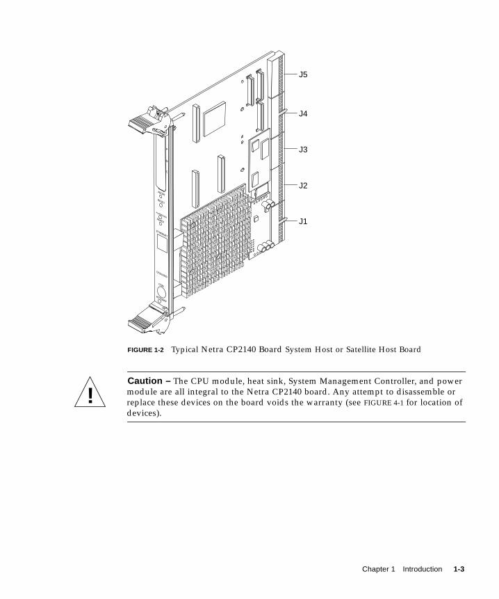
FIGURE 1-2 Typical Netra CP2140 Board System Host or Satellite Host Board
Caution – The CPU module, heat sink, System Management Controller, and powermodule are all integral to the Netra CP2140 board. Any attempt to disassemble orreplace these devices on the board voids the warranty (see FIGURE 4-1 for location ofdevices).
ETHERNET
HOTSWAP
COM
READY
ALARM/USER
CP2010/500
ABORT
C
RESET
M
P
J5
J4
J3
J2
J1
!
Chapter 1 Introduction 1-3

1.1 Netra CP2140 Board SystemConfigurationSystems that conform to CompactPCI specifications require differentiation of chassisboard slots depending upon the mode in which a board is to function.
To function as a System Host, a CP2140 processor includes connections to distributePCI clocks and to receive interrupts from peripherals. It must also be situated in aSystem Host slot in the CompactPCI segment because only these chassis slots havebackplane wiring with the full set of connections required to enable the System Hostfunction. The CP2140 directly controls the CompactPCI peripheral hardware. NetraCP2140 boards assume a System Host role when installed in a PICMG system slot. Asystem slot is marked with an open triangle legend specified in CompactPCISpecification, PICMG 2.0 R3.0.
The CP2140 can be installed in one of the remaining (non-System Host) slots if theuser wants to use it as a Satellite Host.
The simplest configurations of the Netra CP2140 board are shown in FIGURE 1-3. Theycontain one System Host that can supply any input/output (I/O) required by itself(a), or use an added I/O board (b). There is no redundancy in either of thesearrangements.
FIGURE 1-3 Non-redundant Netra CP2140 Board HA Configuration - One System HostBoard
Satellite Hosts do not control any peripheral I/O outside their own board and aretypically used to perform independent processor-intensive tasks.
(a) System host board (b) I/O board added
CompactPCI Bus
SystemHost
I/O
I/O
I/O
CompactPCI Bus
SystemHost
I/O
1-4 Netra CP2140 Technical Reference and Installation Manual • October 2002
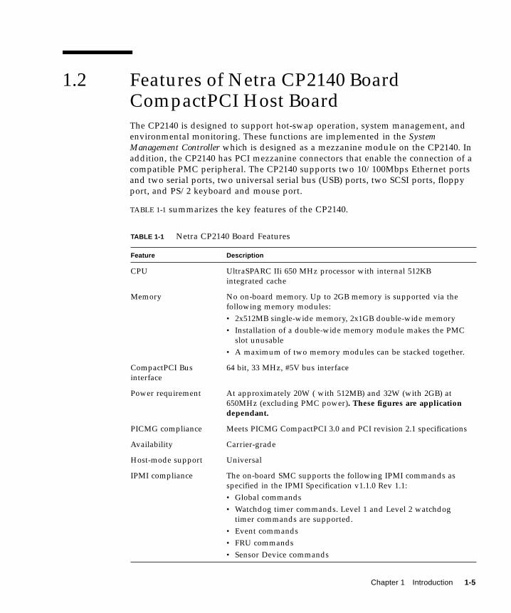
1.2 Features of Netra CP2140 BoardCompactPCI Host BoardThe CP2140 is designed to support hot-swap operation, system management, andenvironmental monitoring. These functions are implemented in the SystemManagement Controller which is designed as a mezzanine module on the CP2140. Inaddition, the CP2140 has PCI mezzanine connectors that enable the connection of acompatible PMC peripheral. The CP2140 supports two 10/100Mbps Ethernet portsand two serial ports, two universal serial bus (USB) ports, two SCSI ports, floppyport, and PS/2 keyboard and mouse port.
TABLE 1-1 summarizes the key features of the CP2140.
TABLE 1-1 Netra CP2140 Board Features
Feature Description
CPU UltraSPARC IIi 650 MHz processor with internal 512KBintegrated cache
Memory No on-board memory. Up to 2GB memory is supported via thefollowing memory modules:• 2x512MB single-wide memory, 2x1GB double-wide memory• Installation of a double-wide memory module makes the PMC
slot unusable• A maximum of two memory modules can be stacked together.
CompactPCI Businterface
64 bit, 33 MHz, #5V bus interface
Power requirement At approximately 20W ( with 512MB) and 32W (with 2GB) at650MHz (excluding PMC power). These figures are applicationdependant.
PICMG compliance Meets PICMG CompactPCI 3.0 and PCI revision 2.1 specifications
Availability Carrier-grade
Host-mode support Universal
IPMI compliance The on-board SMC supports the following IPMI commands asspecified in the IPMI Specification v1.1.0 Rev 1.1:• Global commands• Watchdog timer commands. Level 1 and Level 2 watchdog
timer commands are supported.• Event commands• FRU commands• Sensor Device commands
Chapter 1 Introduction 1-5

Hot-swap support • Basic, Full and HA hot swap supported when installed in theSystem Controller slot of a Sun proprietary HA hot-swapbackplane.
• Supports both basic and full hot-swap functions when installedin the System Controller slot of a standard full hot-swapchassis.
Operating environment Solaris 8 2/02 or subsequent compatible version with CP2000Supplemental CD 4.0 for Solaris 8 (CP2000 Supplemental CD3.1 for Solaris 8 can also be used with the CP2140 board, but itdoes not contain all of the features of CD 4.0).
Ethernet support Dual 10/100Mbit Ethernet with MII interface to the backplane.Ethernet A port is also routed to the front panel with on-boardPHY and magnetics (only front or rear access of this Ethernet Aport is enabled, no simultaneous accesses to this port arepermitted)
I/O • Dual Async serial ports via dual mini-DB9 (non-standard)connectors on transition card
• One console serial port brought to front panel via a DIN 8connector
• Dual USB ports on the transition card. Each USB port is drivenby individual controllers (both USBs routed to the CompactPCIbackplane via the J5/P5 connector)
• IPMI I2C bus is routed to the CompactPCI backplane via J1/P1.This can be bused to all slots on the CompactPCI backplane
• One I2C bus routed to the transition board via the J5/P5connector
BackplaneI/O—accessiblethrough rear transitioncard faceplate
• Two RS 232 serial ports• Two SCSI ports• One cutout to support the use of a PIM card on the transition
card panel.• Access to a floppy port, parallel port, a keyboard and a mouse
port. The use of these ports would consume 2U space.• Provision to add one IHV-supplied PCI Interface Module (PIM)
I/O port when used with transition card
CompactPCI interface • Compliant with PICMG 2.0 R3.0 Compact PCI BusSpecification for 33 MHz PCI speed
• Supports both 32-bit and 64-bit Compact PCI I/O boards• CompactPCI interface supports only +5Volt PCI environment• Compliant with PICMG 2.1 R1.0 Compact PCI hot swap• Specification in Basic, Full and HA hot swap• Compliant either as a System Controller or as a satellite board
TABLE 1-1 Netra CP2140 Board Features (Continued)
Feature Description
1-6 Netra CP2140 Technical Reference and Installation Manual • October 2002

1.3 Hot-Swap SupportThe Netra CP2140 board is capable of performing basic hot swap, full hot swap andhigh-availability (HA) hot swap of a Sun-supported CompactPCI I/O card.
■ Basic hot swap: This feature provides hardware features required to perform hotswap, but an operator is required to execute software steps such as systemconfiguration and installation of device drivers.
Disk interface Dual single ended channel Ultra-SCSI that can support up to40MB/sec data transfer rate. Both SCSI connectors are broughtout to the Transition Card.
PMC support • Supports up to one PMC slot*
• Compliant with CMC Standard IEEE-P1386.1, PMC mezzaninemodules specification
• PMC slot supports only +5V PCI environment• Mapping of 64 user-defined PMC I/O signals to J3/P3 on
CompactPCI backplane• Provision for adding one IHV supplied PMC expansion port on
front panel
PIM support Compliant with PMC I/O Module Standard, VIT 36-199X, DraftVTA Standards Organization. Can be achieved when using Sundesigned transition card for CP2140.
Watchdog timer Two levels of watchdog timer are supported:• Level 1 causes an interrupt to the SPARC processor.• Level 2 causes the system to reset, power down, or power
cycle.
NVRAM/TOD 8KB of non-volatile memory storage and TOD
System flash 1 MB onboard
User flash 8MB (2 x 4MB)
Building compliance NEBS Level 3
Flash update Supported from downloaded file
Physical dimensions Standard 6U CompactPCI form factor. Fits into a singleCompactPCI slot with two memory modules installed.
* One PMC card is supported with the use of single-wide memory module/s. No PMC slot is supported with theuse of double-wide memory module/s.
TABLE 1-1 Netra CP2140 Board Features (Continued)
Feature Description
Chapter 1 Introduction 1-7

■ Full hot swap: This feature provides both hardware and software featuresrequired for software connection protocol. Board software connection controlresources provide the following:
■ ENUM# signal to indicate service requests to the system host, which includeadding or removing software drivers for boards that have been inserted orremoved.
■ Hot-swap switch to indicate that an operator wishes to extract a board.■ LED which is illuminated to indicate that it is safe to remove a board without
interrupting system operation.
■ HA hot swap: In a high-availability (HA) system, hardware and software is addedto enable a higher degree of system control. The following signals are used tocontrol each slot in the system:
■ BD_SEL#: The shortest pin on a system backplane - this pin is the last to mateand first to break contact. This ensures that sensing takes place at a time whenall other pins are reliably connected.
■ HEALTHY#: A radial signal that signals a board is suitable to be released fromreset and allowed onto the PCI bus.
■ PCI-RST#: Driven by the system host, platforms can use this signal to controlthe electrical connection process - boards cannot come out of reset untilHEALTHY# signal is indicated.
1.4 Front Panel I/O Connectors andIndicatorsFIGURE 1-4 illustrates the indicators and I/O connectors on the CP2140 front panel.The front panel connectors, buttons, and LEDs from top to bottom are as follows:
■ One peripheral mezzanine card (PMC) I/O slot
■ ABORT – push button switch; passes an XIR signal to the SMC
■ RESET – A reset push button switch; passes a Button Power-on-Reset (BOR)signal to the SMC
■ ALARM/USER – A red/green (two color) LED — for board status
■ READY – A green power LED, sourced from the power module
■ Ethernet – RJ45 Ethernet connector (10/100 Mbps)
■ COM – 8-pin DIN RS-232 serial I/O port
■ HOT SWAP – A blue LED for hot-swap status, sourced from the SMC
■ A hot-swap latch that has to be closed at insertion of board and opened prior toextraction of the CP2140.
1-8 Netra CP2140 Technical Reference and Installation Manual • October 2002

FIGURE 1-4 Netra CP2140 I/O Front Panel
1.5 Software RequirementsThe CP2140 requires at least the Solaris 8 2/02 operating environment. The CP2000Supplemental CD 4.0 for Solaris 8 is available that offers additional features on theNetra CP2140 board, such as driver support and satellite hot-swap support. TheCP2000 Supplemental CD 3.1 for Solaris 8 can also be used for the CP2140, but doesnot contain all of the features of CD 4.0.
P
M
C
ABORT
RESET
COM
CP2140-650
HOTSWAP
ALARM/USER
READY
microsystems
ETHERNET
Chapter 1 Introduction 1-9
For further information on how to obtain CP2000 Supplemental CD 4.0 for Solaris 8,please contact your Field Application Engineer.
1.6 Determining Netra CP2140 BoardIdentification NumbersThis section provides details on how to identify the Netra CP2140 board.
1.6.1 Netra CP2140 Board Assembly IdentificationFor proper identification of the Netra CP2140 board, labels are provided on theboard (see also FIGURE 1-5):
The Sun barcode label provides the following information:
■ Board part number (for example, 5016358) which is the first seven digits on thebarcode label. The next six digits are the board serial number(for example, 000230).
The Subcon label provides the following information:
■ Product part number (for example, 6403), product dash (for example, 04) andrevision number (for example REV 09).
1-10 Netra CP2140 Technical Reference and Installation Manual • October 2002
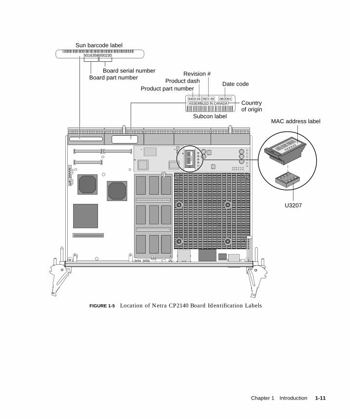
FIGURE 1-5 Location of Netra CP2140 Board Identification Labels
34
SV
49J
12
12
SV
28F
SW
2401S
W1801
12
SV
28F
U3207
XXXXXX
xxxxxx
6403-04ASSEMBLED IN CANADA
REV 09 08/2001
Country of origin
Product dashProduct part number
Date code
Revision #
Subcon label
5016358000230
Sun barcode label
Board part number Board serial number
MAC address label
Chapter 1 Introduction 1-11

1.6.2 Determining Firmware VersionsTo display the OpenBoot PROM version, SMC firmware, PLD and SMC FPGAinformation, type at the OK prompt:
The following is an example of a typical display:
1.6.3 Determining Software VersionTo determine the release number of Solaris operating environment, at the machine-name prompt type:
machine-name% uname -r
The Solaris version displays in the following format: X.X.X or X.X
1.7 Technical Support and WarrantyIf you have any technical questions or issues that are not addressed in the NetraCP2140 Technical Reference and Installation Manual or on the web site, contact yourlocal sales representative. To contact Sun Enterprise Services in the U.S.,phone (800) USA-4SUN (800-872-4786). To find the Sun Enterprise ServicesWorldwide Solution Center nearest you go to this URL:
http://www.sun.com/service/contacting/solution.html
ok .version
SMC Firmware Release 3.4.9 Platform ID 10FPGA Version 1.0PLD Version 1.3Firmware CORE Release 1.0.3 created 2002/4/19 15:2Release 4.0 Version 2 created 2002/04/19 14:47cPOST version 1.0.3 created 2001/9/24ok
1-12 Netra CP2140 Technical Reference and Installation Manual • October 2002

When you call Sun Enterprise Services, be sure to identify the product by theproduct name: Netra CP2140 board. Also provide its part number (see “DeterminingNetra CP2140 Board Identification Numbers” on page 1-10).
The CP2140 comes with a warranty. If your board fails during the warranty period,contact your local Sun Enterprise Services representative for instructions. Before youcall, get the Netra CP2140 board date code, part number, and serial number from thelabels as described in “Determining Netra CP2140 Board Identification Numbers” onpage 1-10.
Chapter 1 Introduction 1-13

1-14 Netra CP2140 Technical Reference and Installation Manual • October 2002

CHAPTER 2
Installation
This chapter describes the system configurations available for the Netra CP2140board and a brief procedure summary. It also describes how to configure the boardand its transition card.
2.1 System ConfigurationsThe Netra CP2140 board can be mounted in various enclosures. It can be deployedin various electrical configurations to suit each end-user’s requirements. Forexample, the host board can be used with a transition card and configured to bootfrom a network as a diskless client. Alternatively, industry-standard PMC and PIMhardware from independent hardware vendors (IHVs) can provide local disk I/Owhich can optionally be used as a boot path. The basic installation procedure isindependent of the type of enclosure used: a floor-mounting rack, a bench-topcabinet, or some other configuration. The memory is user-configurable. SeeFIGURE 2-1 for Netra CP2140 board hardware configuration examples.
2-1

FIGURE 2-1 Examples of Netra CP2140 Board Hardware Configurations
FIGURE 2-1 shows the board hardware configuration options. For more informationyou see the product website at:
http://www.sun.com/products-n-solutions/nep/hardware/boards/cp2140/
Standalone host board operation in benchtop cPCI chassisenclosure
Optional networkconnection
Optional networkconnection
CP2140 host board
CP2140 satellite board
Host board in a 19-inch rack-mountedcPCI system
Backplane withfront and rear I/O cPCIconnectors
Transition cardmodule
CP2140 host board
CP2140 satellite boardCOM
READY
ALARM/USER
ABORT
RESET
M
P
COM
READY
ALARM/USER
ABORT
RESET
M
P
COM
READY
ALARM/USER
ABORT
RESET
M
P
COM
READY
ALARM/USER
ABORT
RESET
M
P
2-2 Netra CP2140 Technical Reference and Installation Manual • October 2002
2.2 Orderable ItemsThe following items that are related to the Netra CP2140 board can be ordered fromSun Microsystems:
■ Host board: Netra CP2140-650 - 1 Gbyte total memory or 2 Gbyte total memory
■ Netra CP2140 board SDRAM memory modules■ XCP2000-MEM-512MB: 512 Mbyte memory mezzanine card■ XCP2000-MEM-1GB: 1 Gbyte memory mezzanine card
■ The CP2000 Supplemental CD 4.0 for Solaris 8.
■ XCP2040-TRN I/O Transition Card (see FIGURE 2-3). This board is compatible withthe Netra CP2140 board.
The customer must obtain the other hardware and software as required:
■ Solaris 8 2/02 operating environment, or subsequent compatible version
■ CompactPCI enclosure to accommodate 6U boards, comprising: chassis,backplane, power supply. FIGURE 2-1 shows a typical configuration. See Chapter 2to ensure that your enclosure meets the power supply and cooling requirementspecifications.
■ Serial terminal or terminal emulation for console output
■ Cables for terminal and network connection
TABLE 2-1 Netra CP2140 Board Hardware Configurations
Configuration and Use Network/ServerChassis Requirements andOther External Hardware
Diskless node (for normal useroperation running at least Solaris 82/02 operating environment)
Requires networkconnection to server
Standard CompactPCIchassis
Standalone operation (for engineeringdevelopment environment)
Can be connected tonetwork and server
Special CompactPCI chassiswith backplane thatprovides front and rear I/Oconnection. Also requiresthe XCP2040-TRN I/OTransition Card.
Carrier-grade rack-mountedconfiguration (for Telco operations)
Network and serverconnection notrequired
Rack-mountable 19 inch x6U chassis
Chapter 2 Installation 2-3

■ PIM and PMC hardware
The Netra CP2140 board can accommodate the addition of IHV-built PMC modulesto access I/O on their front panels. PMC modules decode their custom I/O from thehost’s onboard PCI bus B signals.
The XCP2040-TRN I/O Transition Card is installed from the rear of the CompactPCIenclosure and interfaces with the host board’s I/O connectors J3, J4, and J5 throughthe backplane. The backplane carries two RJ45 ports, two serial ports, two parallelports, one floppy port, two SCSI ports, and two USB ports out to its rear panel.FIGURE 2-2 shows the major components and connectors of the Netra CP2140 board.FIGURE 2-8 shows the physical interface between two Netra CP2140 host boards andtwo transition cards. To see a typical Netra CP2140 board with memory installed seeFIGURE 2-5.
2-4 Netra CP2140 Technical Reference and Installation Manual • October 2002
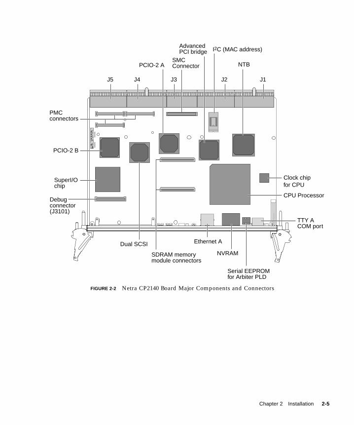
FIGURE 2-2 Netra CP2140 Board Major Components and Connectors
NVRAMSDRAM memorymodule connectors
Ethernet ADual SCSI
Serial EEPROMfor Arbiter PLD
NTB
AdvancedPCI bridge I2C (MAC address)
SMCConnector
J5 J4 J3 J2 J1
PCIO-2 A
Clock chipfor CPU
CPU Processor
PCIO-2 B
PMCconnectors
34
SV
49J
12
12
SV
28F
SW
2401S
W1801
SuperI/Ochip
Debug connector(J3101)
TTY ACOM port
Chapter 2 Installation 2-5

FIGURE 2-3 shows the XCP2040-TRN Transition Card and its connectors.
FIGURE 2-3 XCP2040-TRN Transition Card Connectors
2.3 Preinstallation ChecklistThe Netra CP2140 board installs into a customer-supplied 6U chassis. It is importantto review the information in the following sections before installing the host board.TABLE 2-2 lists the items to check before installing the board.
RS-232 connectorsPIM
12
SV2 6G 12
SV2 6G1
2SV2 6G
Ejector lever
J5 connector
J4 connector
I2C Bus Access Header
Serial EEPROM
J3 connector
USB connector B
USB connector A
10/100BASE-T Ethernet connectors
SCSI B connector
SCSI A connector
2-6 Netra CP2140 Technical Reference and Installation Manual • October 2002

2.3.1 System Checklist■ Check all the parts in the shipment and make sure that the shipment is complete
as indicated in the Netra CP2140 CompactPCI Board Product Note (816-4870-xx).
Make sure that you have received all the contents listed in the product notedocument at the site and that the shipment has cleared the local inventory controlprocedures. If an item is missing or damaged, contact your Sun distributor.
■ Make sure that the switch settings are as indicated in the Netra CP2140CompactPCI Board Product Note (816-4870-xx).
If the switches are not set properly at the factory, contact your Field ApplicationEngineer.
The Netra CP2140 board system requires various other hardware and softwarecomponents which are necessary for proper operation. The OEM customer isresponsible for providing the following components as required:
■ Solaris 8 2/02 operating environment or a subsequent compatible version.
TABLE 2-2 Preinstallation Checklist
Activity Reference
Verify that all required hardware and software have beenreceived and inventoried.
Section 2.3.1, “SystemChecklist” on page 2-7
Read supporting manuals and Web site. Section 2.3.2, “ViewingWeb Pages and ReadingDocuments” on page 2-8
Go over the power budgeting. Section 2.3.3, “PowerBudgeting” on page 2-8
Make sure you have the latest OpenBoot PROM. Section 2.3.4, “Gettingthe Latest OpenBootPROM Version” onpage 2-8
Verify that you have the necessary space to install the hostboard. Verify that proper space, local area networking (LAN),and environmental preparations have been properlycompleted.
Section 2.3.5,“Completing Space,Network, andEnvironmentalPlanning” on page 2-9
Determine the Ethernet and IP address and hostnames and besure they have been properly allocated and registered at thesite.
Section 2.3.6, “DetermineLocal Network IPAddresses and HostNames” on page 2-9
Chapter 2 Installation 2-7

■ A chassis (enclosure) that complies with standard CompactPCI form factor with apower supply that must provide sufficient power for all the components.
■ Memory modules. A minimum of 512 Mbyte memory is required to run theSolaris™ operating environment.
■ Keyboard (PS/2 keyboard or standard USB).
■ Mouse (PS/2 mouse or standard USB).
■ Verify that you have the necessary space to install the host board. Verify thatproper space, local area networking (LAN), and environmental preparations havebeen properly completed.
■ Determine the Ethernet and IP addresses and host names and be sure they havebeen properly allocated and registered at the site.
■ Make sure you have the latest OpenBoot PROM. See Chapter 6 for details.
2.3.2 Viewing Web Pages and Reading DocumentsThe latest product information along with technical manuals are available on theWeb. It is important to read the Netra CP2140 Product Note document (816-4870-xx)that is shipped with the board. For online documents and other information relatedto the Netra CP2140 board, visit the following Web site:
http://www.sun.com/products-n-solutions/hardware/docs/CPU_boards/
2.3.3 Power BudgetingTo determine your power supply requirements see Chapter 3.
2.3.4 Getting the Latest OpenBoot PROM VersionThe Netra CP2140 board requires the latest OpenBoot PROM compatible with yourSolaris operating environment. The board is shipped with the version of OpenBootPROM available at the time of manufacture (version 4.0.x). The OpenBoot PROMmight be out-of-date by the time you get this board.
For the latest OpenBoot PROM version, go to the product website:
http://www.sun.com/products-n-solutions/nep/hardware/boards/cp2140
2-8 Netra CP2140 Technical Reference and Installation Manual • October 2002

2.3.5 Completing Space, Network, and EnvironmentalPlanningEnsure that the proper physical, electrical, and environmental preparations havebeen completed before the installation. For a list of the Netra CP2140 boardspecifications, see Chapter 2. Make sure that the following conditions are met:
■ The enclosure supports the sum of the specified maximum board power loads.
■ The enclosure supports the cooling and airflow requirements. See Section 3.1.5,“Environmental Specifications” on page 3-5.
■ The facility power load supports the rack or enclosure power requirements.
■ The Netra CP2140 board fits a standard CompactPCI chassis. If your installationrequirements are different, contact your Field Application Engineer (FAE).
2.3.6 Determine Local Network IP Addresses and HostNamesYou must have the following information to configure the local area network (LAN).Make sure that the IP addresses are not duplicated on different servers (ifseparated).
■ IP addresses and host names on this network for each Netra CP2140 board client.(Local IP addresses are not needed if they are assigned by a network DHCPserver.)
■ Domain name
■ Type of name service and corresponding name server names and IP addresses (forexample, DNS and NIS (or NIS+)
■ Subnet mask
■ Gateway router IP address
■ NFS server names and IP addresses
■ Web server URL
Note – You might need the MAC (Ethernet) addresses of the local hosts to makename server database entries. The MAC address is displayed in the console outputwhile booting to the ok prompt. It can also be derived from the host ID seen on thelabel of the MAC address (SEEPROM) package (MAC = 8.0.20.hostid). The differentnetwork services can be located on a single server to simplify the configuration.
Chapter 2 Installation 2-9

2.4 SafetyCarefully read the Important Safety Information for Sun Hardware Systems (816-7190-xx)document included in your board kit and the following statements before you installor remove any part of the system.
Caution – Installation of this product requires specific training and technicalknowledge. These instructions have been provided for use by Sun Microsystemstrained personnel. This equipment uses electrical power internally that is hazardousif the equipment is improperly assembled or disassembled. Although this and someother boards are designed for hot-swap operation, other components must not besubjected to such stresses. Do not disassemble or service the system if the power isconnected to the chassis. Follow all safety procedures to avoid injury to personneland damage to equipment. Before you begin to install or remove a board or anyother components, make sure the system power is turned off and the system powercord is removed from the AC source.
The host board and other boards are extremely sensitive to damage fromelectrostatic discharge (ESD) caused by the build-up of electrical potential onclothing and other materials.
Follow these safety and ESD preventive measures:
■ Before connecting, disconnecting, or handling boards or peripherals, attach oneend of the ground strap to your wrist and the other end to a grounded surface.
■ Keep the boards in the antistatic bags until they are needed.
■ Remove a board from its antistatic bag only when you are properly groundedwith a ground strap.
■ Place the boards only on an antistatic mat. Do not place boards on top of anantistatic bag unless the outside of the bag also has antistatic protection.
2.5 Installation Procedure SummaryHere are the general steps to configure, install, and set up a Netra CP2140 boardsystem. Ensure that the guidelines outlined in Section 2.3, “Preinstallation Checklist”on page 2-6 are met before configuring and installing the board.
1. Configure the Netra CP2140 board and the associated hardware.
2-10 Netra CP2140 Technical Reference and Installation Manual • October 2002

2. Install the CP2140 into an enclosure (see Section 2.10, “Installing the NetraCP2140 Board” on page 2-18).
3. Install the XCP2040-TRN Transition Card.
4. Connect a SCSI interface, if applicable to your system. Connect the SCSI interfacewith a cable to one of the SCSI connectors on the XCP2040-TRN Transition Card.Also connect any other necessary cables to the XCP2040-TRN Transition Card. Forfurther details, see Section 2.13, “Connecting Devices to a XCP2040-TRN I/OTransition Card” on page 2-27.
5. Install the Solaris operating environment (see Section 2.15, “Software Installation”on page 2-30).
6. Connect the CP2140 to the server using existing Ethernet lines or run the CP2140as a standalone system (see Section 2.17, “Standalone Operation” on page 2-32).
7. Set up the system that is using the CP2140.
8. Power on the CP2140 client.
9. Run related applications.
2.6 Materials and Tools RequiredThis section provides information on the materials and tools required to performinstallation. The minimum tools required to perform installation are:
■ Straight slot screwdriver, 1/4 inch■ Phillips screwdrivers, No. 1, No. 2■ Antistatic wrist strap■ Needle nose pliers■ Terminal
Chapter 2 Installation 2-11

2.7 Configuring the Netra CP2140 BoardHardwareThis section describes how to configure related hardware such as memory modules,PMC modules, and the XCP2040-TRN Transition Card. Most of this hardware mustbe configured before the CP2140 is installed.
2.7.1 Installing Memory ModulesThe CP2140 can accommodate both single- and double-wide memory modules.FIGURE 2-4 shows two typical memory modules used on the Netra CP2140 board.
TABLE 2-3 Netra CP2140 Board I/O Hardware Configurations
I/O Hardware Required Description
Ethernet XCP2040-TRN I/OTransition Card—suppliedas an option
Default boot path uses Ethernet port on Transition Card;host runs in diskless client configuration
SCSI XCP2040-TRN I/OTransition Card, two SCSIconnectors and internalconnectors
Can be used for local boot. Use SCSI interface on theXCP2040-TRN I/O Transition Card.
Serial data XCP2040-TRN I/OTransition Card
Serial A port on optional transition card is path of defaultconsole I/O
USB XCP2040-TRN I/OTransition Card
Can be used for keyboard I/O for use with video graphics
2-12 Netra CP2140 Technical Reference and Installation Manual • October 2002

FIGURE 2-4 Single- and Double-wide Memory Modules
Up to two modules in any supported memory configuration can be installed in anycombination (512 Mbyte, 1 Gbyte). However, if two memory modules need to beinstalled and one of the modules is double-wide, the double-wide module should beinstalled first (on the bottom). Refer to Section 3.1.2, “Main Memory” on page 3-3 fora list of possible memory module configurations.
FIGURE 2-5 shows a typical SDRAM memory module installed on a CP2140.
Single-widememory module
Double-widememory module
Chapter 2 Installation 2-13

FIGURE 2-5 A Typical Netra CP2140 Board with Memory Modules Installed
2.7.2 PMC Module InstallationThe PCI Mezzanine Card (PMC) is installed on J3001, J3002, and J3003 connectors onthe motherboard. These connectors interface with the matching connectors on thePMC board: PN1, PN2, and PN4, respectively. The PMC is secured with twomounting posts and screws. Refer to the user documentation from the PMC cardmanufacturer on how to install the PMC module. FIGURE 2-6 shows how the PCIMezzanine Card is installed.
2-14 Netra CP2140 Technical Reference and Installation Manual • October 2002

FIGURE 2-6 Installing the PCI Mezzanine Card
J3002
J3
J3003
J3001
PN4
User IO
CompactPCIBackplane Connectors
PMC I/O (typical example)
PN2
PN1
Chapter 2 Installation 2-15

2.8 Configuring Transition Card HardwareThis section provides information on installing PIM assemblies and replacing theSerial EEPROM.
2.8.1 Installing PIM AssembliesRefer to the user documentation from the PIM manufacturer on how to install thePIM module.
2.8.2 Replacing the Serial EEPROMThis device is installed on the motherboard at the factory. This step is not necessaryunless you are installing a replacement board that does not have the host ID. If youmust return the CP2140 to the factory, remove this EEPROM from the board beforeshipping it to the factory. The Serial I2C EEPROM is the MAC address carrier and itstores the backup copy of the board MAC address and host ID information (seeSection 5.1.3.4, “Serial I2C EEPROM” on page 5-3).
2-16 Netra CP2140 Technical Reference and Installation Manual • October 2002

FIGURE 2-7 Replacing the Serial I2C EEPROM
The CP2140 supports the Serial I2C EEPROM. If you must replace the CP2140,remove the Serial I2C EEPROM from the original board and install it on the newCP2140.
To correctly position the EEPROM and to precisely install it on the CP2140, seeFIGURE 2-7.
34
SV
49J
12
12
SV
28F
SW
2401S
W1801
12
SV
28F
xxxxxx
U3207
XXXXXX
Chapter 2 Installation 2-17

2.9 Installing the XCP2040-TRN I/OTransition CardRefer to the installation procedure detailed in the XCP2040-TRN I/O Transition CardManual for Netra CP2040/CP2140 CompactPCI Board (806-6743-xx) for installing theXCP2040-TRN Transition Card.
2.10 Installing the Netra CP2140 BoardFollow all the safety rules described in Section 2.4, “Safety” on page 2-10 wheninstalling any hardware into the CompactPCI chassis enclosure.
A number of CompactPCI chassis enclosures come with an internal power supplyand fan. FIGURE 2-8 shows two Netra CP2140 boards (system host and satellite host)being installed in a CompactPCI chassis.
Smaller CompactPCI enclosures have four board slots. One of these slots is reservedfor one 6U form factor board, while the remaining three slots are for either 3U or 6Uboards. The larger eight-slot enclosures have two 6U and six 3U slots. In addition,some special CompactPCI enclosures are equipped with a backplane that enablesboard connection to the front and rear of the chassis.
A CompactPCI chassis contains:
■ A system slot, usually on the far left (viewed from the front) whose position isindicated by a triangle symbol visible on the backplane (if the chassis meets thePICMG 2.0 CompactPCI Specification).
■ Seven peripheral slots (for a single-segment chassis). Peripheral slots areidentified by a circle symbol visible on the backplane.
Note – The CP2140 can be installed in either a peripheral slot or in a system slot.
1. Ensure that power is disconnected from the chassis.
The CP2140 can be installed while the chassis is powered-on—however, this methodis recommended only when absolutely necessary.
2-18 Netra CP2140 Technical Reference and Installation Manual • October 2002

2. Check that the corresponding XCP2040-TRN I/O Transition Card is installed.
Install the transition card before installing the Netra CP2140 board. This step isimportant if the chassis is powered-on during the installation. The transition card isnot hot-swappable. Take the step as a safety precaution.
3. Slide the CP2140 into the appropriate slot on the corresponding top and bottommounting rails and towards the backplane while gently keeping the boardhandles pushed inward (see FIGURE 2-8 and FIGURE 2-9).
While pushing the board, ensure that the CP2140 extraction levers are alignedperpendicular to the card flange in the unlocked position and that the boardconnectors are aligned with the transition card connectors.
4. Install two screws at the top and bottom of the front connector plate to secure theboard.
Chapter 2 Installation 2-19
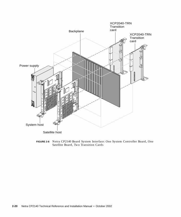
FIGURE 2-8 Netra CP2140 Board System Interface: One System Controller Board, OneSatellite Board, Two Transition Cards
Power supply
XCP2040-TRNTransitioncard
Satellite host
System host
BackplaneXCP2040-TRNTransitioncard
ETHERNET
HOTSWAP
COM
READY
ALARM/USER
CP2010/500
ABORT
C
RESET
M
P
ETHERNET
HOTSWAP
COM
READY
ALARM/USER
CP2010/500
ABORT
C
RESET
M
P
2-20 Netra CP2140 Technical Reference and Installation Manual • October 2002

FIGURE 2-9 Netra CP2140 Board Installation (Close-up View)
The transition card can also be fitted with IHV-supplied PCI interface modules(PIMs) which are configured to bring I/O channels to the unit rear panel. A unit ofPIM hardware is a kit that includes a card for the PMC slot and a card for the PIMslot on the transition card. A PIM is essentially a rear-panel extension added to aPMC module.
Card guide
Card guidepin hole
ETHERNET
HOTSWAP
COM
READY
ALARM/USER
CP2010/500
ABORT
C
RESET
M
P
Chapter 2 Installation 2-21

Note – If the PMC card (used with the PIM) has front I/O connectors, when youconfigure PIM rear connector I/O, the front I/O connectors will not be functional.
You can order the XCP2040-TRN Transition Card, build a compatible custom card, orbuy from an IHV. A minimal set of I/O must provide for a boot path for the hostboard and a path for console I/O to deliver commands and to read board andsystem status.
2.11 Connecting Cables to the Netra CP2140BoardThis section describes how to connect cables to a computer that contains the CP2140.
1. Connect the Ethernet (if required) where shown in FIGURE 2-3.
2. Use the tip utility on the host system to establish a full-duplex terminalconnection with the system containing a CP2140.
3. At the UNIX® prompt in a command tool or shell tool, type:
tip -9600 /dev/ttya
4. Connect a serial cable to Port A (COM port) on the CP2140 or TTYA port of theXCP2040-TRN I/O Transition Card of the target system and to the serial port of thehost system.
Note – Use shielded cables that are grounded at both ends for serial and USB ports.
5. Connect any other peripheral devices (such as a printer) to the appropriateconnector.
6. Power on the system that contains the CP2140 to run the power-on self-tests(POST).
■ If POST is successful, install the appropriate Solaris software package on thesystem (see Section 2.15, “Software Installation” on page 2-30).
■ Read the following caution carefully before plugging devices into theXCP2040-TRN I/O Transition Card.
2-22 Netra CP2140 Technical Reference and Installation Manual • October 2002
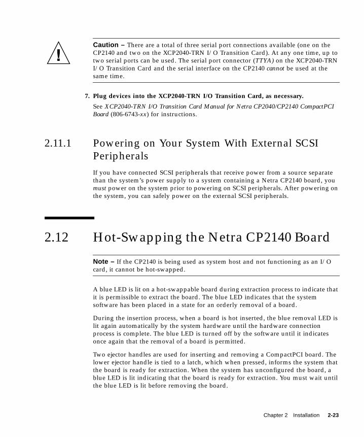
Caution – There are a total of three serial port connections available (one on theCP2140 and two on the XCP2040-TRN I/O Transition Card). At any one time, up totwo serial ports can be used. The serial port connector (TTYA) on the XCP2040-TRNI/O Transition Card and the serial interface on the CP2140 cannot be used at thesame time.
7. Plug devices into the XCP2040-TRN I/O Transition Card, as necessary.
See XCP2040-TRN I/O Transition Card Manual for Netra CP2040/CP2140 CompactPCIBoard (806-6743-xx) for instructions.
2.11.1 Powering on Your System With External SCSIPeripheralsIf you have connected SCSI peripherals that receive power from a source separatethan the system’s power supply to a system containing a Netra CP2140 board, youmust power on the system prior to powering on SCSI peripherals. After powering onthe system, you can safely power on the external SCSI peripherals.
2.12 Hot-Swapping the Netra CP2140 Board
Note – If the CP2140 is being used as system host and not functioning as an I/Ocard, it cannot be hot-swapped.
A blue LED is lit on a hot-swappable board during extraction process to indicate thatit is permissible to extract the board. The blue LED indicates that the systemsoftware has been placed in a state for an orderly removal of a board.
During the insertion process, when a board is hot inserted, the blue removal LED islit again automatically by the system hardware until the hardware connectionprocess is complete. The blue LED is turned off by the software until it indicatesonce again that the removal of a board is permitted.
Two ejector handles are used for inserting and removing a CompactPCI board. Thelower ejector handle is tied to a latch, which when pressed, informs the system thatthe board is ready for extraction. When the system has unconfigured the board, ablue LED is lit indicating that the board is ready for extraction. You must wait untilthe blue LED is lit before removing the board.
Chapter 2 Installation 2-23

2.12.1 Basic Hot-SwappingThe basic hot swap is initiated by the cfgadm configure/unconfigure administrationcommand:
The cfgadm command provides configuration administration operations ondynamically reconfigurable hardware resources. Configuration administration isperformed at attachment points, places where system software supports dynamicreconfiguration of hardware resources during continued operation of the Solarisoperating environment.
Configuration administration distinguishes between hardware resources that arephysically present in the server and hardware resources that are configured andvisible to the Solaris software. The nature of configuration administration functionsare hardware-specific and are performed by calling hardware-specific libraries. Referto the man pages (by typing man cfgadm) for additional information on the optionsassociated with this command.
1. Type the unconfiguration command:
# cfgadm -c unconfigure pci1:hsc0_slot5
To inform the system to enable the extraction and insertion of a device, ifpermissible. The blue LED is lit if the process is successful, indicating that the boardcan be extracted.
2. Remove the I/O board and set it aside.
3. Slide the new I/O board into the top and bottom mounting rails in the same slotinto the backplane while gently keeping the board handles in the open position.Once the board is all the way in, lock the ejector handles (see FIGURE 2-10).
The blue LED is lit once the board makes complete contact with the backplane. TheLED goes off shortly after the ejector handles are closed, if the hardwareinitialization of the board is successful. Otherwise, it remains lit, indicating that theboard must be replaced.
4. Once the blue LED of the board is off, secure the board to the chassis.
5. Type the configuration command:
# cfgadm -c configure pci1:hsc0_<slot5>
The part of the command in parenthesis indicates the slot in which the board resides.
6. Take any other step necessary for board-specific configuration.
2-24 Netra CP2140 Technical Reference and Installation Manual • October 2002

2.12.2 Full Hot-SwappingHot-swapping a line card does not require the system power to be turned off. Referto the chassis manufacturer’s documentation for slot assignments and additionalinformation. In addition, a full hot-swap board does not require running the cfgadmadministrative command. The system automatically configures the card for using thesystem resources. The board-specific configuration steps are still necessary after thecompletion of host-specific configuration.
Follow these steps to hot-swap a line card in a chassis that contains the NetraCP2140 system host board.
1. Remove the I/O board screws.
2. Release the latches of the I/O board and wait for the blue LED to light.
3. Remove the I/O board and set it aside.
4. Slide the new I/O board into the top and bottom mounting rails in the same slotinto the backplane while gently keeping the board handles in the open position.Once the board is all the way in, lock the ejector handles (see FIGURE 2-10).
FIGURE 2-10 shows how to release and to lock the CP2140 injector/ejector handles.
The blue LED is lit once the board makes a complete contact with the backplane. TheLED goes off shortly after the ejector handles are closed, if the hardwareinitialization of the board is successful. Otherwise, it remains lit, indicating that theboard must be replaced.
5. Once the blue LED of the board is off, install two screws at the top and bottom ofthe front connector plate to secure the board.
Chapter 2 Installation 2-25

FIGURE 2-10 Releasing and Locking the Netra CP2140 Board Injector/Ejector Handles
Lock
Unlock
Lock
Unlock
2-26 Netra CP2140 Technical Reference and Installation Manual • October 2002
2.13 Connecting Devices to a XCP2040-TRNI/O Transition CardThe XCP2040-TRN I/O Transition Card is an interface card that provides access tothe following connector features which are supported by the CP2140:
■ Two USB ports■ Two TTY ports■ Two Ethernet ports■ Two SCSI ports■ KB (PS/2 keyboard)■ KB (PS/2 mouse)■ FLOPPY■ PARALLEL■ PIM
Install the XCP2040-TRN I/O Transition Card as directed in the transition cardmanual.
Note – To comply with NEBS Level 3 Intrabuilding Lightning Surge Tests(Telecommunications Port), the intrabuilding cabling must be shielded and theshield must be grounded at both ends. Refer to GR-1089-CORE, Section 4.5.9.
1. Connect a single-ended SCSI drive and cable to the internal SCSI connector onthe XCP2040-TRN I/O Transition Card.
The internal SCSI connector is more suitable for attaching internal devices to thesystem.
Caution – For SCSI A, both internal and external SCSI connectors are on the sameSCSI A bus. Use only one connector at a time to avoid signal problems on the SCSIchain. Also, the SCSI cable cannot exceed more than 9 feet (3 meters) in length toavoid possible data errors.
2. Connect other supported peripheral devices as required.
Note – For a detailed description of the XCP2040-TRN I/O Transition Card, refer toXCP2040-TRN I/O Transition Card Manual for Netra CP2040/CP2140 CompactPCI Board(806-6743-xx).
!
Chapter 2 Installation 2-27

2.13.1 Adding CompactPCI Cards and Drivers to aNetra CP2140 Board SystemThe CP2140 configuration supports IHV CompactPCI cards. To add CompactPCIcards and drivers, refer to the documentation provided with the CompactPCI card.Usually software drivers and related documentation are provided on the CD orfloppy diskettes. Read all documentation furnished with the package. Themanufacturer’s Web site might also have the latest product and driver information.
2.13.1.1 To Install a CompactPCI Card
1. Halt the operating environment and power down the system.
2. Install the CompactPCI card.
3. Make necessary connections.
4. Power up the system.
5. Boot with -r option (or with -rv for verbose messages).
6. At system prompt, become superuser.
7. Add package using pkgadd command.
8. Reboot if necessary.
Note – In a properly configured system, a card can be hot inserted and thenmanually configured by unsing cfgadm.
2.13.1.2 To Verify That the Board is Recognized by the System
1. Use the prtconf -D command to display the device tree.
It should show the PCI bus instances #0 and #1 for the two PCI buses on the CP2140.There are instances of various PCI cards connected to each one. A PCI card mightshow up as pciVVVV,DDDD, where VVVV is the vendor ID, for example, 1011 andDDDD is the device ID, for example 008e. If the driver for the card is already loaded,then you might see the device name supplied by the driver in the device tree.
2. Use the modinfo command to see whether the driver for the card is loaded.
Typically the description of the driver contains the name of the product or thevendor.
2-28 Netra CP2140 Technical Reference and Installation Manual • October 2002

3. At the OpenBoot PROM prompt, the PCI board is visible in the device tree even ifthe driver is not installed.
2.13.1.3 To Obtain Additional Assistance
1. Run the following commands and record the output.
prtconfmodinfodmesgcat /etc/driver_aliasescat /etc/path_to_inst
2. Contact the PCI card vendor.
2.13.2 Backplane and Cardcage ConsiderationsTo successfully run a Netra CP2140 board system, consider the following pointsrelated to the CompactPCI backplane and cardcage:
■ For CompactPCI connector information see Appendix A.
■ Power supply requirements for backplane and cardcage (for more details seeChapter 3.)
■ Cooling fan requirement.
■ Overtemperature conditions.
■ Shock and vibration standards (see Section 3.1.7, “Compliance” on page 3-6).
2.14 Initial Power-On and Firmware UpdateThis section describes the power-on procedure for the CP2140. This procedure isintended only for advanced UNIX users and system administrators.
1. Power up the system.
a. Position the power supply switch to ON.
b. Use the tip utility to establish a full-duplex terminal connection between theSun workstation and the CP2140.
c. At the UNIX prompt in a command or shell tool window type:tip -9600 /dev/ttya
Chapter 2 Installation 2-29

2. Perform the following diagnostic steps.
a. Verify the accuracy of the following information before continuing to the nextstep.
■ Valid memory configuration is displayed on the banner.
■ Valid Ethernet address is displayed on the banner.
b. At the ok prompt, type:
ok probe-scsi-all
Make sure all devices are recognized by the system. Ensure that the hard diskdrive is recognized as target 0 and that the CD-ROM drive is recognized astarget 6.
c. At the ok prompt, type:
ok .version
For details on output information, see Section 6.6, “Determining FirmwareVersion” on page 6-18.
2.15 Software InstallationThe CP2140 requires the Solaris 8 2/02 operating environment software. CP2000Supplemental CD 4.0 for Solaris 8 is available that offers additional features for theCP2140 such as CompactPCI net driver support and satellite hot-swap support.CP2000 Supplemental CD 3.1 for Solaris 8 can also be used with the Netra CP2140board, but does not contain all of the features available on CD 4.0.
For further information on how to obtain the CD, contact your Field ApplicationEngineer.
■ To install the system from the CD , go to Step 1.
■ To install the system from a network, go to Step 2.
1. To install the system from the CD , at the ok prompt, enter:
ok boot cdrom
The system boots from the CD and the Solaris operating environment installationbegins. Provide appropriate answers to various prompts that are displayed as thesystem is installed.
2. To install the system from a server, obtain the boot client Ethernet address (thesystem being built).
2-30 Netra CP2140 Technical Reference and Installation Manual • October 2002
a. At the ok prompt (on the system being built), type:
ok banner
The Ethernet address displayed in the following format: X:X:XX:XX:XX:XX forexample: 8:0:20:7e:f6:dc
b. Type the Ethernet address obtained in Step a into the install server as a bootclient.
Refer to the Solaris software documentation to set up an install server.
c. At the ok prompt on the client (of the system being built), type:
ok boot net
The system boots from the network and the Solaris software is installed from thenetwork. Various prompts are displayed as the system is installed; answer themas appropriate.
3. After the Solaris operating environment is installed, at the ok prompt, enter:
ok boot disk -rv
The system configures itself after the installation.
If the installation is successful, the system boots to a Solaris login prompt.
2.16 Setting Up a NetworkThe minimal necessary infrastructure to enable network computing involves a bootserver with networking software and the CP2140. The boot server senses the CP2140booting up on the network and supplies the client with its boot image: Solarissoftware.
Note – The Netra CP2140 board also depends on a domain network server (DNS)and a network information server (NIS); do not attempt to set up clients on anetwork without them.
An administrator can also choose a separate Internet Message Access Protocolversion 4 (IMAP4) server and a home directory server. These software services canbe installed on a single server or spread out over several servers.
Follow these guidelines to help ensure a successful CP2140 client/serverconfiguration.
■ Install the CP2140 clients on the same subnet as the boot server. You cannot bootacross a gateway or router. The CP2140 boot process uses a Trivial File TransferProtocol (TFTP) broadcast to receive a secondary boot program called
Chapter 2 Installation 2-31
inetboot.jd from the server. Messages using TFTP are automatically disabledas a security measure in routers. The boot process might be changed in futureproduct releases to enable booting across routers. Application or Web servers donot have to be on the same subnet and can be accessed across a router or gateway.
■ Do not configure a CP2140 to more than one boot server. You cannot havemultiple boot servers attached to the same client.
■ Avoid using the UNIX command-line interface to set up the client/servernetwork. Use the available client configuration tools from the WebTop Serversoftware environment. The configuration tools have an easy-to-use graphical userinterface (GUI).
2.17 Standalone OperationThe CP2140 provides a complete I/O subsystem and can operate as a standalonecomputer for development purposes or other special applications. The CP2140provides two UltraWide single-ended SCSI connections that are accessible throughthe rear of a special CompactPCI chassis that contains a backplane. This enablesconnection to a hard drive, tape, or a number of other SCSI devices. Software can bedownloaded through the internet or from a CD into a hard drive connected to theXCP2040-TRN I/O Transition Card.
2-32 Netra CP2140 Technical Reference and Installation Manual • October 2002

CHAPTER 3
Netra CP2140 Board Specifications
This chapter provides the Netra CP2140 board specifications.
3.1 Board Features and SpecificationsTABLE 3-1 shows the physical dimensions of the CPU board.
Described below is some information on CompactPCI height restrictions and theNetra CP2140 board standard components.
The CompactPCI standard, PICMG 2.0 Rev 3, calls out the maximum componentheights of 13.71 +/- 0.03 mm. Due to variations in parts, board flatness, boardthickness, and manufacturing tolerances, the stacked height of two expansionmemory boards and memory turrets installed on a CP2140 board may exceed thislimit.
PICMG 2.0 R3 and IEEE 1101.10-1996 require 2.54mm between the top ofcomponents and the separation plane, and there is at least approximately 0.5mm to2mm of clearance to solder-side components or leads of an adjacent board from thatsame separation plane. Therefore, there is very little chance that a small specificationviolation will impact an adjacent card in a PICMG 2.0 R3 compliant chassis.
TABLE 3-1 Netra CP2140 Board Physical Dimensions
CPU Board Parameter 6U CompactPCI Form Factor
Height 233.35 mm
Depth 160 mm
Width 19.80 mm
3-1
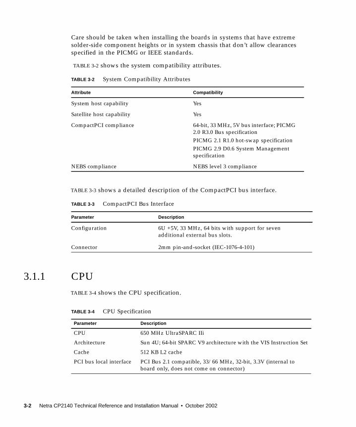
Care should be taken when installing the boards in systems that have extremesolder-side component heights or in system chassis that don’t allow clearancesspecified in the PICMG or IEEE standards.
TABLE 3-2 shows the system compatibility attributes.
TABLE 3-3 shows a detailed description of the CompactPCI bus interface.
3.1.1 CPUTABLE 3-4 shows the CPU specification.
TABLE 3-2 System Compatibility Attributes
Attribute Compatibility
System host capability Yes
Satellite host capability Yes
CompactPCI compliance 64-bit, 33 MHz, 5V bus interface; PICMG2.0 R3.0 Bus specificationPICMG 2.1 R1.0 hot-swap specificationPICMG 2.9 D0.6 System Managementspecification
NEBS compliance NEBS level 3 compliance
TABLE 3-3 CompactPCI Bus Interface
Parameter Description
Configuration 6U +5V, 33 MHz, 64 bits with support for sevenadditional external bus slots.
Connector 2mm pin-and-socket (IEC-1076-4-101)
TABLE 3-4 CPU Specification
Parameter Description
CPU 650 MHz UltraSPARC IIi
Architecture Sun 4U; 64-bit SPARC V9 architecture with the VIS Instruction Set
Cache 512 KB L2 cache
PCI bus local interface PCI Bus 2.1 compatible, 33/66 MHz, 32-bit, 3.3V (internal toboard only, does not come on connector)
3-2 Netra CP2140 Technical Reference and Installation Manual • October 2002

3.1.2 Main MemoryTABLE 3-5 shows the memory specification.
TABLE 3-6 shows the Netra CP2140 board memory module configurations.
Note – The memory module configurations provided in TABLE 3-6 are theconfigurations that have been tested and are supported. Other memoryconfigurations are possible on the Netra CP2140 board but customers will notreceive technical support if they use other memory configurations.
Any two modules in any supported memory configuration can be installed in anycombination (512 Mbyte, 1 Gbyte). However, if two memory modules need to beinstalled and one of the modules is double-sized, it should be installed on thebottom.
If a double-sized memory module is installed on the Netra CP2140 board, then theinstallation of a PMC card is not supported.
TABLE 3-5 Memory Specification
Parameter Description
Memory size—min 512 MB
Memory configuration—soldered No soldered memory
Memory configuration—stackable Up to two custom stackable modules; see TABLE 3-6for allowable combinations
Memory type 3.3V, DRAM with ECCLVTTL-compatible CMOS; configured on bus widthof 64-bit + 8-ECC bits
Interface Unbuffered
TABLE 3-6 Netra CP2140 Board Memory Module Configurations
Bottom SDRAM ModulePN and Specification
Top SDRAM ModulePN and Specification
Total MemoryAvailable on Board
375-3025-xx512MB
375-3025-xx512MB
1024MB
375-3026-xx*
1024MB
* The 1024MB (part no. 375-3026-xx) is a double wide memory module.
375-3026-xx1024MB
2048MB
Chapter 3 Netra CP2140 Board Specifications 3-3
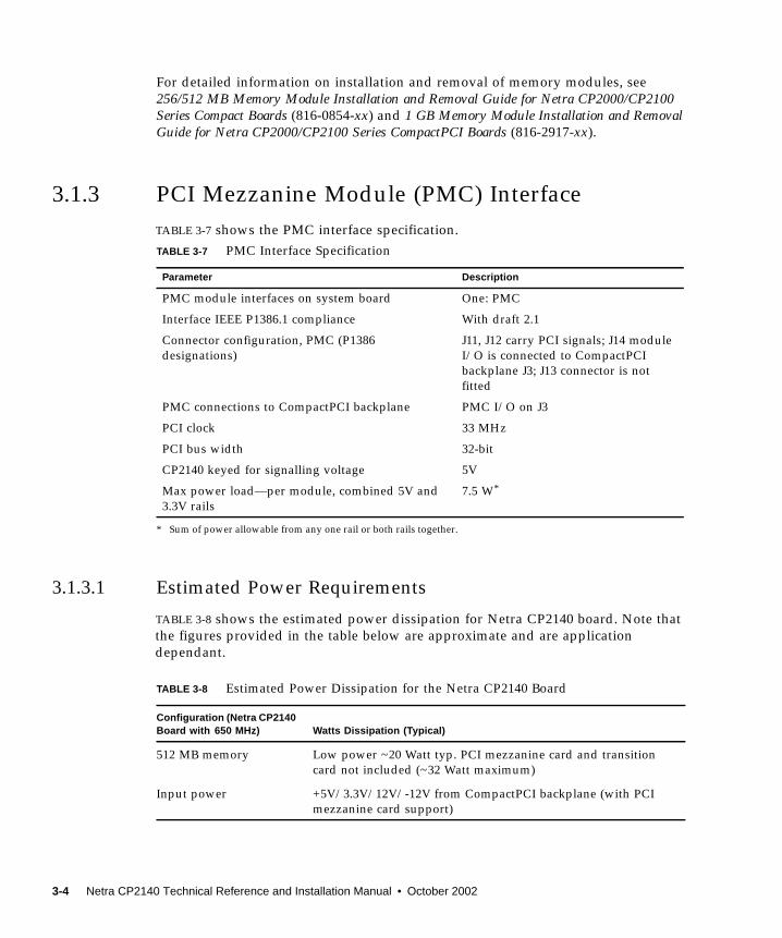
For detailed information on installation and removal of memory modules, see256/512 MB Memory Module Installation and Removal Guide for Netra CP2000/CP2100Series Compact Boards (816-0854-xx) and 1 GB Memory Module Installation and RemovalGuide for Netra CP2000/CP2100 Series CompactPCI Boards (816-2917-xx).
3.1.3 PCI Mezzanine Module (PMC) InterfaceTABLE 3-7 shows the PMC interface specification.
3.1.3.1 Estimated Power Requirements
TABLE 3-8 shows the estimated power dissipation for Netra CP2140 board. Note thatthe figures provided in the table below are approximate and are applicationdependant.
TABLE 3-7 PMC Interface Specification
Parameter Description
PMC module interfaces on system board One: PMC
Interface IEEE P1386.1 compliance With draft 2.1
Connector configuration, PMC (P1386designations)
J11, J12 carry PCI signals; J14 moduleI/O is connected to CompactPCIbackplane J3; J13 connector is notfitted
PMC connections to CompactPCI backplane PMC I/O on J3
PCI clock 33 MHz
PCI bus width 32-bit
CP2140 keyed for signalling voltage 5V
Max power load—per module, combined 5V and3.3V rails
7.5 W*
* Sum of power allowable from any one rail or both rails together.
TABLE 3-8 Estimated Power Dissipation for the Netra CP2140 Board
Configuration (Netra CP2140Board with 650 MHz) Watts Dissipation (Typical)
512 MB memory Low power ~20 Watt typ. PCI mezzanine card and transitioncard not included (~32 Watt maximum)
Input power +5V/3.3V/12V/-12V from CompactPCI backplane (with PCImezzanine card support)
3-4 Netra CP2140 Technical Reference and Installation Manual • October 2002

3.1.4 MechanicalThe Netra CP2140 board complies with the mechanical specifications found in theCompactPCI specification PICMG 2.0 R3.0.
3.1.5 Environmental SpecificationsTABLE 3-9 shows the environmental conditions and limits.
TABLE 3-9 Environmental Conditions and Limits
Ambient Conditions Lower Limits*
* Short term, in this column, refers to a period of not more than 96 consecutive hours and a total of not more than15 days in 1 year.
Upper Limits*
Transportation and storagetemperature
-40˚ C for 72 hrs. max. +70˚ C for 72 hrs. max.
Transportation and storagehumidity
5% relative humidity, non-condensing
95% relative humidity, non-condensing
Operating temperature 0˚ C (-5˚ C short term) 40˚ C (55˚ C short term)
Operating humidity 5% relative humidity, non-condensing
85% RH (90% relativehumidity short term) non-condensing
Shock and vibration As stated in NEBS GR-63 CORE specifications, section 4.3.1and 4.3.2 for shock criteria and 4.4.3 for vibration criteria;MIL-STD 810E, Method 514.4, CAT IMIL-STD 810E, Method 516.4, II-3.2
Electrostatic discharge GR-1089 Section 2
Altitude 0 foot to 10,000 feet operational (0 meter to 3408 meters)
Cooling 300 linear feet per minute (LFM) (minimum requirement)
Chapter 3 Netra CP2140 Board Specifications 3-5

3.1.6 Reliability and AvailabilityReliability prediction is the first measurement point of expected behavior of theinherent design mean time between failures (MTBF) of the product.
TABLE 3-10 shows the reliability prediction for board level MTBF.
3.1.7 ComplianceAll printed wiring boards (PWBs) are manufactured by UL recognizedmanufacturers, and have a flammability rating of 94-V1 or better. Compliance withEMI and safety regulations for products including the Netra CP2140 board isentirely the responsibility of OEMs. The Netra CP2140 board has passed FCC ClassB tests in representative enclosures.
The Netra CP2140 boards are intended to be incorporated into systems meeting thefollowing regulations and compliances:
■ USA FCC part 15 Class B■ USA Safety UL 1950■ Canadian ICES Class B■ Canadian Safety CSA C22.2 Number 950■ European Union EMC CE Mark EN55022 and EN50082-1■ European Union Safety CE Mark EN 60950■ European Union Safety TÜV■ Japanese EMC VCCI Class B■ NEBS Level 3
Board requirements for NEBS Level 3 criteria provide the highest assurance ofproduct operability with minimal service interruptions over the life of theequipment. The requirements include the following categories and all associatedsections and subcategories:
■ NEBS GR-63-CORE, Issue 1, October 1995 - Network Equipment-BuildingSystem Requirements: Physical Protection
TABLE 3-10 Reliability Prediction for Board Level MTBF
Items MTBF (hours)Annualized FailureRate (AFR in%)†
† AFR (%) is Annualized Failure Rate based on 8,760 power on hours (POH) per year
CP2140 board* + 2x512 MB memory
* Board ambient temperature at 40˚ C
163,878 5.35
CP2140 board + 2x1 GB memory(double wide)
136,647 6.41
XCP 2140-TRN card 823,050 1.06
3-6 Netra CP2140 Technical Reference and Installation Manual • October 2002

■ GR-1089-CORE, Issue 2, Revision 1, February 1999 - ElectromagneticCompatibility and Electrical Safety - Generic Criteria for NetworkTelecommunications Equipment
Note – Refer to the note in Section 2.13, “Connecting Devices to a XCP2040-TRNI/O Transition Card” on page 2-27.
3.1.8 SafetyPlease read the cautionary note provided below.
Caution – The Netra CP2140 board holds a lithium battery attached to the real-timeclock, The battery is not a customer replaceable part. Do not dispose of battery infire. Do not attempt to disassemble or recharge it. Failure to comply may cause thebattery to explode.
Chapter 3 Netra CP2140 Board Specifications 3-7

3-8 Netra CP2140 Technical Reference and Installation Manual • October 2002

CHAPTER 4
Hardware Description
This chapter summarizes the CP2140 hardware. See Chapter 5 for a detailedfunctional description of the hardware.
4.1 PhysicalThe CP2140 is a 6U-sized circuit card with CompactPCI connectors J1 and J2 forCompactPCI, and J3 - J5 for I/O.
■ The CP2140 provides front-panel I/O through an RJ45 connector, a TTYconnector, and a slot for a PMC card.
■ Through the CompactPCI backplane, a transition card can be connected toprovide connector access for two serial ports, two RJ45 Ethernet ports, two USBports, one parallel port, one floppy port, PS/2 keyboard/mouse, and two SCSIports.
■ The PMC card interface accepts an IHV-supplied PMC I/O card.
■ The IHV-supplied PCI Interface Module (PIM) can duplicate front-panel PMCI/O ports. The PIM interfaces with a transition card and enables access to I/Oports at the rear of the enclosure.
A PMC module can be installed on the CP2140. A cut-out is provided on the front-panel for the PMC card. The CP2140 front panel also provides an RJ45 Ethernetconnector and a mini-DIN TTY connector. The panel includes status lamps and resetpush buttons which are listed top to bottom as follows (see FIGURE 1-4):
■ ABORT – push button■ RESET – push button■ ALARM/USER – red/green■ READY – green■ Blue LED for hot swap■ Front panel latch to lock and unlock the CP2140 for insertion or removal.
4-1
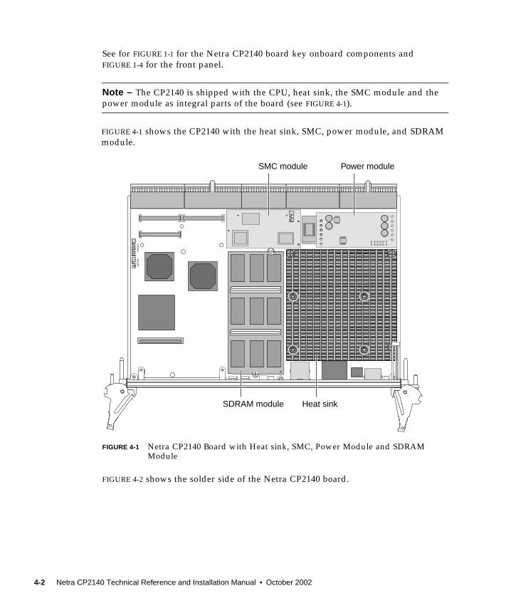
See for FIGURE 1-1 for the Netra CP2140 board key onboard components andFIGURE 1-4 for the front panel.
Note – The CP2140 is shipped with the CPU, heat sink, the SMC module and thepower module as integral parts of the board (see FIGURE 4-1).
FIGURE 4-1 shows the CP2140 with the heat sink, SMC, power module, and SDRAMmodule.
FIGURE 4-1 Netra CP2140 Board with Heat sink, SMC, Power Module and SDRAMModule
FIGURE 4-2 shows the solder side of the Netra CP2140 board.
SDRAM module Heat sink
SMC module
34
SV
49J
12
12
SV
28F
SW
2401S
W1801
12
SV
28F
Power module
4-2 Netra CP2140 Technical Reference and Installation Manual • October 2002
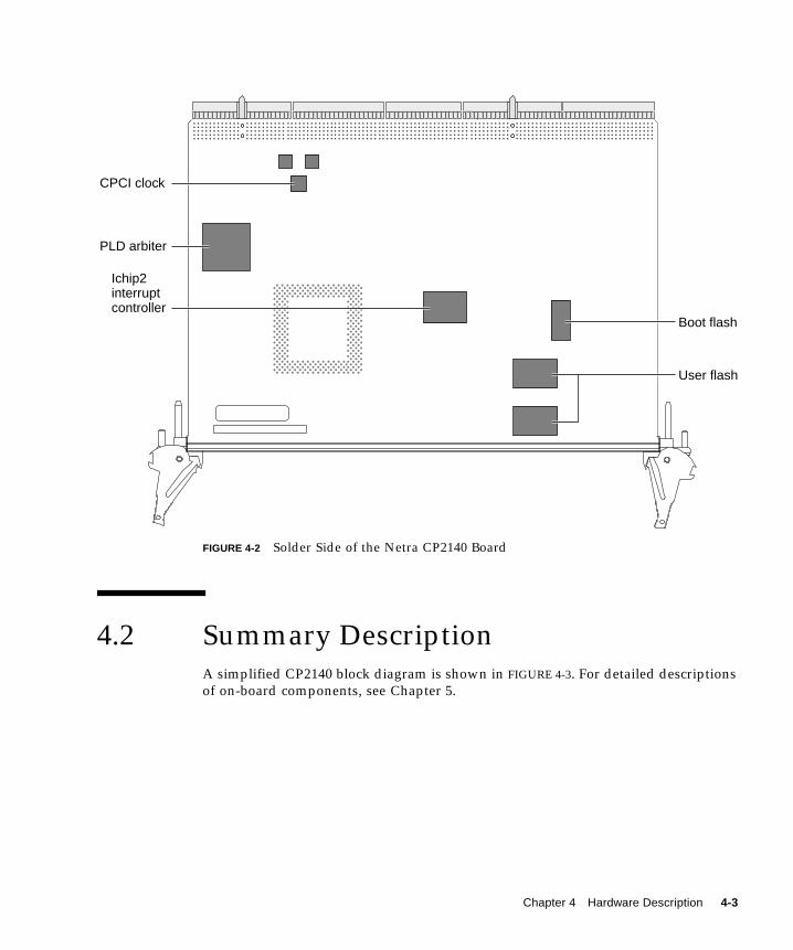
FIGURE 4-2 Solder Side of the Netra CP2140 Board
4.2 Summary DescriptionA simplified CP2140 block diagram is shown in FIGURE 4-3. For detailed descriptionsof on-board components, see Chapter 5.
User flash
Boot flash
PLD arbiter
Ichip2interruptcontroller
CPCI clock
Chapter 4 Hardware Description 4-3

FIGURE 4-3 Netra CP2140 Board Functional Block Diagram
The UltraSPARC IIi processor has a 512 Kbyte 4-way set associative integrated cache.
Apart from incoming interrupts, the processor handles all I/O through its built-in66MHz, 32-bit PCI bus interface. This interface is used to connect to an AdvancedPCI Bridge (APB) that services two 33 MHz, 32-bit downstream interfaces:PCI bus A and PCI bus B.
PCI bus A connects to a nontransparent PCI bridge (NTB) which services theprincipal PCI bus connection to the CompactPCI backplane through connectors J1and J2. In a System Host role, a PCI bus arbiter provides arbitration signals for theCompactPCI backplane bus. It also supplies clocks for the CompactPCI bus. Thearbiter is only active if the host board functions in a System Host role. When theboard is required to function as a satellite board, the CompactPCI bus arbiter isdisabled by the System Management Controller (SMC).
PCI Bus B connects the APB to each of two PCIO-2 (SouthBridge) packages: PCIO-2A and PCIO-2 B, the Dual SCSI device and PMC slot.
PowerModule
SDRAM Module
SDRAM Module
System SlotSystem Host
CompactPCIInterface
SMC/ASM
BMC
Flash Memory
I2CIPMIEthernet(2)USB(2)Serial(2)
I/O
PMC
CPUProcessor
PCI BusInterface
66 MHz32-bit PCI
33 MHz32-bit PCI-A
64-bit + ECC83 MHzSDRAM
33 MHz32-bit PCI
KeyboardMouseParallelFloppySCSI (2)
User-defined I/OFront or BackPanel Access
8-bit EBus
4-4 Netra CP2140 Technical Reference and Installation Manual • October 2002

PCIO-2 A provides downstream interfaces:
■ Network media-independent interface (MII) A to the CompactPCI/J4 connectorand to an on-board PHY package A that interfaces the front panel of RJ45
■ USB A port that is routed through CompactPCI/J5 backplane connector
■ The EBus is a versatile 8-bit data, 24-bit address bus similar to an ISA bus. EBus Aconnects to:
■ NVRAM, which stores real-time clock and MAC address information
■ System and user flash memory
■ Main PLD, which provides EBus decodes for chip selects and CompactPCIarbiter control logic
■ Super I/O PC97307 interface
PCIO-2 B provides the following interfaces:
■ Network MII B to the CompactPCI/J4 connector
■ USB B port that is routed through CompactPCI/J5 backplane connector
■ EBus B connects to the System Management Controller (SMC) to complete theUltraSPARC host-SMC communication path.
The PCI bus B from the APB connects to a 33 MHz, 32-bit PMC interface on the hostboard and the SCSI 53C876E from LSI.
The SMC features are:
■ The bus arbiter enabling it to control CompactPCI bus arbitration, clock, and resetfunctions
■ The onboard I2C bus, enabling it to communicate with sensors and controls
■ The User IPMI bus, enabling user management of other entities in the system.Peripheral hot-swap control is also enabled through this path.
The SMC activates the power module and controls the system reset signals. Inaddition, it handles high-availability (HA) hot-swap signals from the CompactPCIbackplane. For example, ENUM, HEALTHY, BD_SEL, and PCI_RST (the PCI resetsignal).
Chapter 4 Hardware Description 4-5

4-6 Netra CP2140 Technical Reference and Installation Manual • October 2002

CHAPTER 5
Functional Description
This chapter provides a functional description of the Netra CP2140 board, includingfunctional blocks of the board, block diagrams, user interface, and various functionsrelated to Netra CP2140 boards.
FIGURE 5-1 shows a detailed block diagram of the CP2140.
FIGURE 5-1 Netra CP2140 Board Detailed Block Diagram
Note – CP2140 memory and SMC circuits are on mezzanine modules.
StackableSDRAMModule
NTB
CPUProcessor
PCI_CPU_Bus(66 MHz, 32-bit)
PCIClocks
Clocks
PHY RJ45
Ser
FrontPanelLEDsSwitch
Arbiter
TempSense I2C GPIO
Boot Flash1 MB
CompactPCIClock Gen.
CPCI Pull-up/Termination IC
CompactPCI J1,J2
SMCModule
LSI53C876 PCIO-2 B PCIO-2 A SuperI/OPMC
I2CDevicesUser Flash
8 MB
IChip2Interrupt
Controller
AdvancedPCI Bridge
(APB)
PowerModule
BP_12V
12V
BP_5V
BP_3.3V
MEM_Bus(64-bit+ECC)
PCI_A_Bus(33 MHz,32-bit)
CP_Bus(33 MHz, 64-bit)
BP_CP_Bus(33 MHz, 64-bit)
PCI_B_Bus(33 MHz,32-bit)
I2C Bus
EBus_A
EB
us_B
IPM
IBP_-12V
5V
3.3V
VDDCORE
1V
-12V
CompactPCI J3,J4,J5 Connectors
PIM
SC
SI
US
B
CP
CI H
otsw
ap
MII
US
B
Flo
ppy
Par
KbdMs
Ser
(2)
MII
5-1

5.1 Functional BlocksThe main functional blocks of the Netra CP2140 board are provided in this section.
5.1.1 UltraSPARC IIi Processor
FIGURE 5-2 UltraSPARC IIi Interface
The UltraSPARC IIi 650-MHz processor is based on the 64-bit SPARC V9architecture. This 4-way superscalar CPU processor has integrated memorycontroller, PCI controller and 512 KBytes of L2 cache. The processor is directlyconnected to the board SDRAM through an ECC path.
5.1.2 SDRAM MemoryThe Netra CP2140 board has no on-board memory. The memory is composed of upto two mezzanine memory modules. Each mezzanine memory module has two 100-pin male connectors on its bottom surface which plug into corresponding femaleconnectors (J0601 and J0602) on the system board. The module also has two of thesame type of female connectors on its top side for memory expansion. Up to twomemory modules can be stacked. The CP2140 memory system supports up to twostackable 512 Mbyte/1024 Mbyte Synchronous DRAM (SDRAM) memory modulesin any combination.
Clocks ResetInterrupts
JTAGTest Signals
SDRAM Interface72-bit ECC
Dual-address Bus
PCI Interface32-bit, 66 MHz
CPUProcessor
VDDIO VDDCORE
5-2 Netra CP2140 Technical Reference and Installation Manual • October 2002

5.1.3 Firmware
5.1.3.1 System (Boot) Flash Memory
A 1 Mbyte x 8-bit system flash device resides in one megabyte of space. It containsCommon Operations and Reset Environment (CORE) firmware, comprehensivePOST, and OpenBoot PROM boot code. The system flash can be upgraded byrunning a program out of OpenBoot PROM or by executing a Solaris software script.If the system flash becomes corrupted for any reason, contact your Field ApplicationEngineer.
5.1.3.2 User Flash Memory
The board is equipped with 8 Mbytes of user flash memory, which is used to housedropins. Dropins simplify customizing a system for the user.
5.1.3.3 NVRAM
The use an 8 K-bit x 8 timekeeper SRAM (NVRAM) package. This componentprovides:
■ Battery backup using a removable lithium battery with an approximate ten-yearlife
■ A time-of-day (TOD) real-time clock with an accuracy of 1 sec/day■ 8 Kbytes storage for environment variables, user modifiable. The Ethernet address
and host ID are stored in the NVRAM.■ On firmware boot up, the Ethernet address stored in the NVRAM is compared
against the backup copy stored in the Ethernet serial EEPROM on the CP2140 andis updated if it differs from the backup copy.
Note – To ensure proper function, replace NVRAM only with the same orequivalent type recommended by the manufacturer. Dispose off used batteriesaccording to the manufacturer’s instructions.
5.1.3.4 Serial I2C EEPROM
The serial I2C EEPROM, also called the MAC address carrier, stores the backup copyof the board MAC address and host ID in a removable serial EEPROM that isaccessible through the I2C bus. OpenBoot PROM supports retrieving the Ethernetaddress from the EEPROM, deriving host ID, and downloading this data to the
Chapter 5 Functional Description 5-3

NVRAM. The user can remove and retain this EEPROM for future use in case theboard needs to be shipped to the factory for replacement. The replacement board isnot shipped with an EEPROM.
5.2 Clock FrequenciesTABLE 5-1 shows the clock frequencies on the CP2140 components:.
5.3 Bus SubsystemsThere are three internal PCI buses on the CP2140:
■ PCI_CPU Bus—32-bit, 66MHz, UltraSPARC IIi primary bus interface (onboardonly)
■ PCI_A Bus—32-bit, 33 MHz, APB A bus interface
■ PCI_B Bus—32-bit, 33 MHz, APB B bus interface
There is also an external CompactPCI bus driven to and from the backplane.
TABLE 5-1 Clock Frequencies
Components Frequencies
CPU processor 650 MHz
MC12429 250 MHz
MC12429 XTAK 325 MHz
CY2292 XTAL 14.38181 MHz
Memory 92.86 MHz
CPU APB 66 MHz
PCI / CompactPCI 33 MHz
SuperI/O 24 MHz
USB 48 MHz
Ethernet 25 MHz
SCSI 40 MHz
12C 6 MHz
5-4 Netra CP2140 Technical Reference and Installation Manual • October 2002

One of the internal PCI buses, PCI bus B, is bridged to two lower-speed buses: EbusA and EBus B. PCI bus A communicates with the CompactPCI backplane throughthe nontransparent PCI bridge (NTB) as shown in FIGURE 5-3.
FIGURE 5-3 Netra CP2140 Board PCI Bus Interface
5.3.1 APB PCI Bus InterfacesThe UltraSPARC IIi processor has an integrated 32-bit, 66 MHz PCI bus interface.The Advanced PCI Bridge (APB) splits this bus into two 32-bit, 33 MHz PCI buses.Of these, the PCI A bus connects to the PCI nontransparent bridge (NTB) whichforms the interface to the CompactPCI backplane. The PCI B bus connects to twoPCIO-2 bridges. Each of these bridges carries an EBus and peripheral interface at theother end.
5.3.2 PCIO-2 A and PCIO-2 B Devices and EBus PathsThe two PCIO-2 bridges connect between two APB devices PCI bus B and theirperipheral interfaces at their other ends. Each of these bridges carries one EBusinterface. The EBus is similar to the ISA bus and runs at comparable speed. It is usedto interface slower internal peripherals.
EBus A connects PCIO-2 A to:
CPUProcessor
NTB
CompactPCIBackplaneCPCI-J1/J2
32-bit66 MHz
32-bit33 MHz
64-bit33 MHz CP_Bus
PCI_A_Bus
PCI_CPU_Bus
APB
Sun PCIO-2Ethernet/USB
& EBus
SCSIChip
32-bit, 33 MHz
PCI_B_Bus
PMC Slot Aw/Front Panel& CPCI-J3 I/O
Sun PCIO-2Ethernet/USB
& EBus
Chapter 5 Functional Description 5-5

■ System flash EEPROM. The UltraSPARC IIi processor accesses system flashEEPROM through the APB and PCIO-2 A.
■ User flash EEPROM■ NVRAM■ Serial I/O through a dual universal asynchronous receiver/transmitter (DUART)
device
EBus B connects PCIO-2 B to the System Management Controller (SMC). This path isthe primary means of communication between the UltraSPARC IIi host and the SMCand is used to transfer host commands to it.
The UltraSPARC IIi processor expects access to a boot PROM/flash which isnormally mapped onto the EBus and requires that the EBus device be directlyaccessible to the UltraSPARC IIi processor.
5.3.3 CompactPCI BusFIGURE 5-4 shows the CompactPCI bus interface.
FIGURE 5-4 CompactPCI Bus Interface
This part of the CP2140 interfaces to the CompactPCI backplane. It is a 64-bit, 33MHz interface that conforms to the PICMG 2.0 D3.0 Compact PCI Specification and thePICMG 2.1 R1.0 Hot Swap Specification. In order to operate in satellite or nonhostmode, its interface requires the following:
■ Hot-swap capable, nontransparent PCI-to-PCI bridge
■ 10-ohm series termination resistor for every CompactPCI bus input
cPCISeries Term/
Pullup/Precharge
Circuit
NTB
cPCIBackplane
ClockGeneration
ExternalArbiter for
cPCIBackplane
cPCIBackplanecPCI-J1/J2
BP_CP_AD<63..0>
BP_CP_CTRL
BP_CP_CLK<7..1> CP_CLK<0>
CP_AD<63..0>
PCI_CPU_AD<31..0>
PCI_CPU_CTRL
CP_CTRL
5-6 Netra CP2140 Technical Reference and Installation Manual • October 2002

■ 1V precharge bias (Vp) for every CompactPCI bus input
The latter two requirements (series termination and precharge bias) are provided bya custom integrated circuit to save on board space and reduce complexity.
The CompactPCI bus circuit includes a system slot (host CPU) functionality whichentails the following:
■ Providing the external arbiter for the CompactPCI backplane■ Providing PCI clocks to all slots on the CompactPCI backplane■ Providing bus pull-ups for all signals on the CompactPCI backplane
In addition, the host CPU also provides the Baseboard Management Controller(BMC) functions described in Section 5.3.6, “System Management Controller” onpage 5-9.
As seen in FIGURE 5-1, there are three interfaces to the CompactPCI circuit: the 64-bitCompactPCI backplane, the CompactPCI clock generation, and the output from thebridge onto the PCI_CPU bus.
5.3.4 System I/OThis section describes the CP2140 system I/O features. FIGURE 5-5 shows the CP2140I/O interface.
FIGURE 5-5 Netra CP2140 Board I/O Interface
The CP2140 I/O subsystems are onboard SCSI and SuperI/O, which provide twosingle-ended UltraWide SCSI ports, one parallel port, one floppy port, two serialports, one keyboard port, and one mouse port.
Each PCIO-2 ASIC provides 10/100BASE-T Ethernet, as well as a USB port.
Switches and LEDs RJ45 SER(1)
J1-J2 J3-J5
CP2140 BoardBackplane Connectors
PMC_A FP I/OFront Panel
MII_A
PHY
RJ45
MII_B TransitionCard
PHY
RJ45 Floppy SER(2) PAR SCSI(2) USB(2) PS2KB/MS
I2C
PMC_A BP I/O
PMC_A BP PIM
IPMI
Chapter 5 Functional Description 5-7

Access to CP2140 system I/O is provided either partially through the front panel orthrough the XCP2040-TRN transition card that attaches to the CompactPCIbackplane connectors J3-J5 as shown in FIGURE 5-5.
The PMC module provides either front-panel I/O ports or sends user-definedI/O to the backplane/transition card, where a PIM connector is available to attachthe PMC card I/O connector and provide rear-panel I/O access.
I/O to the front panel includes:
■ LEDs - Power, Status, and Hot Swap (blue)■ Microswitches - POR and XIR (eXternal Interrupt Request)■ RJ45 10/100BASE-T Ethernet■ Serial A (via mini-DIN 8 connector, also available to transition card)■ PMC front panel I/O cutout
I/O through the backplane through the transition card includes:
■ Two Ethernet (MII to backplane, two RJ45 connectors out of transition card)■ I/O (floppy, serial A and B, parallel, keyboard, mouse) provided by SuperI/O■ Dual SCSI■ Two universal serial bus (USB) ports provided by PCIO-2s■ PMC/PIM module cutout for PMC rear panel I/O■ I2C to the transition card for identification
5.3.5 PMC and PIM InterfaceThe PCI Mezzanine Card (PMC) interface is defined by IEEE and PICMG standards.The PMC interface enables independent hardware vendor (IHV) PMC cards to beused to implement a particular I/O interface choice from the host at the systemintegration level. This choice is independent of any I/O that is provided by theprimary hardware. The PMC connectors are provided on the CP2140 to providemodular front panel I/O expansion via a slim mezzanine card mounted parallel tothe host computer. This is for user-defined I/O front or back panel access.
Note – The Netra CP2140 board supports one PMC card when single-sized memorymodules are used. No PMC card is supported with the use of double-sized memorymodules.
A compatible XCP2040-TRN I/O transition card is installed at the rear of thebackplane that provides for the attachment of matching IHV-supplied PCI InterfaceModule (PIM) hardware. The PIM hardware comprises a PMC module which mayor may not carry an I/O connector on its front flange. It enables the PIM card toconnect to the transition card PIM sockets. These items together can duplicate the
5-8 Netra CP2140 Technical Reference and Installation Manual • October 2002

PMC front-panel interface at the transition card panel which is at the rear of theenclosure. Examples of such interfaces are a display controller, Ethernet, SCSI, or T1or T3 communications channels.
FIGURE 5-6 shows the PCI mezzanine module interface on the host board.
FIGURE 5-6 PCI Mezzanine Module Interface on Host Board
The APB on the CP2140 supplies PCI bus signals to PMC connectors J3001 and J3002.The PMC card logic decodes its specific I/O interface which it makes available at thefront panel. J3003 is specified for user I/O and carries PMC signals to CompactPCIbackplane connector J3.
5.3.6 System Management ControllerFIGURE 5-7 shows the system management controller interface.
Motherboard
I/O Transition Card
J3
PMC
PIM
I/O Connector
Chapter 5 Functional Description 5-9

FIGURE 5-7 System Management Controller Interface
The System Management Controller (SMC) provides two main functions:
■ The Advanced System Maintenance (ASM) capability, which involves monitoringand controlling the local state using an I2C interface. Some functions performedby the ASM unit include temperature sensing, voltage sensing, power on/offcontrol, board self-configuration.
■ The BMC and/or Peripheral Management Controller function as defined by thePICMG Hot Swap Specification using an IPMI link through the backplane tocommunicate with other slots. Since CP2140 can operate in both the system andsatellite slots of a CompactPCI HA/hot-swap backplane, the SMC must be able toprovide both BMC and Peripheral Management Controller functionality.
As shown in FIGURE 5-7, the SMC interface consists of two parts: the internal/localboard interface for ASM and host processor communications, and the interface to theCompactPCI HA/hot-swap backplane.
ASM functions of the SMC include:
■ Temperature sensing■ Module and board ID (SPD)■ Module control (such as power on/off)■ Local CPU/OS communication via EBus■ Receive System/CompactPCI reset events to generate local board reset
Backplane interface functions of the SMC include:
■ IPMI communications to Baseboard Management Controller■ Interface with hot-swap (Healthy/ENUM/PRESENT) related signals■ Generate/Receive System/CompactPCI reset events to generate local board reset
CompactPCI HA System Backplane
IPMI
CP2140 Board
System Management Controller
BP RSTHA Signals
CPU Processor(via PCIO-2 EBus)
Power ModuleMotherboardReset Control
Power ModuleMemory Module
MotherboardI2C/ASM Devices
Host Bus I2C Local RST
5-10 Netra CP2140 Technical Reference and Installation Manual • October 2002

5.3.7 Watchdog TimerIn the Netra CP2140 board, the SMC implements a two-level watchdog timer. Thehost-SMC command interface defines communication between host and SMC. Thehost and the SMC constantly communicate with each other when the watchdogtimer is enabled. The SMC monitors the heartbeat of the CPU processor host. Theheartbeat is sent in the form of reset watchdog timer from the CPU to the SMC. Itmust be programmed to ensure that it does not get too close to the expiration. Thereshould be some time accounting for the latency overhead or unexpected event thatmay delay transmission of the heartbeat.
For additional information on the watchdog timer, contact your Field ApplicationEngineer.
The two levels of the watchdog timer are as follows:
■ Countdown register timer (16 bits, 100 msec. resolution)■ Pre-timeout timer (1 sec. resolution)
The two watchdog timers are enabled by messages sent over the host-SMCcommand interface using the set watchdog timer command. The commands enabledin the host-SMC command interface for watchdog timer functionality are:
■ Reset watchdog timer■ Set watchdog timer■ Get watchdog timer
TABLE 5-2 descibes the uses of these functions.
5.4 Reset and InterruptsThis section describes the CPU Reset, Reset Modes and Interrupts.
TABLE 5-2 Host-SMC Commands
Host-SMC Command Use For
Reset watchdog timer Starting-restarting watchdog timer from the initial countdownvalue
Set watchdog timer Initializing, configuring and stopping the watchdog timer
Get watchdog timer Retrieval of current settings and present timer value of watchdogtimer
Chapter 5 Functional Description 5-11

5.4.1 CPU ResetThis section lists the reset sequences followed during power on and power off.
5.4.1.1 Power On
The power-on reset process is as follows:
1. Power supply is turned on.
2. POWER_OK is asserted by power supply.
3. System sequences the release of reset.
4. CPU reset is released last.
5. CPU propagates the PCI_RST_L to PCI devices.
6. CPU retrieves the first instruction.
5.4.1.2 Power Off
The power-off reset process is as follows:
1. Power supply fails.
2. POWER_OK is immediately deasserted.
3. System reset is asserted.
4. PCI_RESET_L is asserted.
5. CPU stops executing.
5.4.2 Reset ModesThis section describes the reset modes for system slot and peripheral slot operationsfor the Netra CP2140 board when used in various roles and CompactPCI slots.
TABLE 5-3 describes the available modes of operation in response to a reset request onthe CompactPCI backplane. Determination of system or peripheral slot/satelliteoperation is made from the state of the CompactPCI backplane SYSEN# signal asspecified in the PICMG 2.0 R 3.0 Specification. Note that the RESET# signal has noeffect on the System Management Bus or its associated Intelligent PeripheralMicrocontrollers.
5-12 Netra CP2140 Technical Reference and Installation Manual • October 2002

The default setting for the Netra CP2140 board is mode 66, giving standard systemcontroller operation when the board is installed in the system slot and standaloneoperation for use in peripheral/satellite slots.
Note – You can reprogram the operating mode from the OpenBoot PROM prompt,then reboot the system for the new reset mode to take effect. Some of these modesmight be incompatible with various PICMG Specifications. You need to consider therisk associated with reprogramming these modes.
TABLE 5-3 Available Reset Operating Modes
Reset Mode System Slot Peripheral/Satellite Slot
11 The board generates normalCompactPCI RESET# and PCIsignalling for the backplane in itsrole as system controller.
Backplane reset is propagated tothe SPARC, the 21555 bridge andother resetable components on theboard, resulting in a completereset of the SPARC section of theboard.
22 Standalone Mode. The boardgenerates a constant CompactPCIRESET# and does not respond toany CompactPCI transaction onthe backplane.
Standalone Mode. The localCompactPCI bridge is held inreset, isolated from theCompactPCI bus. The board doesnot respond to any PCItransaction on the CompactPCIbus.
66 Standard System Slot Operation.The board generates normalCompactPCI RESET# and PCIsignalling for the backplane in itsrole as a system controller.
Standalone Mode. The localCompactPCI bridge is held inreset, isolated from theCompactPCI bus. The board doesnot respond to any PCI signallingon the CompactPCI bus.
Chapter 5 Functional Description 5-13

FIGURE 5-8 shows the simplified Reset paths.
FIGURE 5-8 Simplified Reset Paths
Portions of the system are powered by early power before the SPARC domain receivespower (backend power). See Section 5.5, “Power Subsystem” on page 5-15. At theonset of early power, the SMC is reset.■ When the SMC is reset, the whole system is reset.■ When the CPU is reset, the CPU I/O and the NTB are reset.
NTB
CompactPCI Backplane
CPUProcessor
XIR_LP_RST_L
PCI_CPU_RST_L
SYS_RST_L
IO
Micro-controller
APBSPARCPowerDomain
EarlyPowerDomain
SMC
SMC internal reset
Vcc, Vdd,Vdd_core
Power Module
ON/OFF
PWR_OK
EarlyPower
BackplanePower
Early Power orIPMI power
EarlyPower
FPGA
5-14 Netra CP2140 Technical Reference and Installation Manual • October 2002
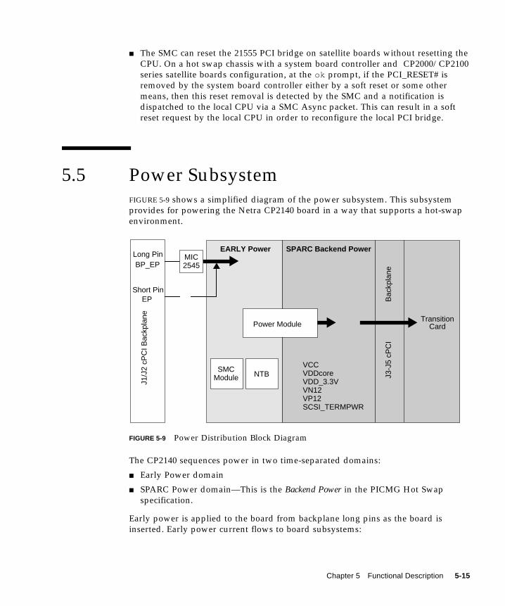
■ The SMC can reset the 21555 PCI bridge on satellite boards without resetting theCPU. On a hot swap chassis with a system board controller and CP2000/CP2100series satellite boards configuration, at the ok prompt, if the PCI_RESET# isremoved by the system board controller either by a soft reset or some othermeans, then this reset removal is detected by the SMC and a notification isdispatched to the local CPU via a SMC Async packet. This can result in a softreset request by the local CPU in order to reconfigure the local PCI bridge.
5.5 Power SubsystemFIGURE 5-9 shows a simplified diagram of the power subsystem. This subsystemprovides for powering the Netra CP2140 board in a way that supports a hot-swapenvironment.
FIGURE 5-9 Power Distribution Block Diagram
The CP2140 sequences power in two time-separated domains:
■ Early Power domain
■ SPARC Power domain—This is the Backend Power in the PICMG Hot Swapspecification.
Early power is applied to the board from backplane long pins as the board isinserted. Early power current flows to board subsystems:
EARLY Power SPARC Backend Power
Bac
kpla
neJ3
-J5
cPC
I
J1/J
2 cP
CI B
ackp
lane Transition
Card
Long Pin
Short Pin
BP_EP
EP
MIC2545
Power Module
SMCModule NTB
VCCVDDcoreVDD_3.3VVN12VP12SCSI_TERMPWR
Chapter 5 Functional Description 5-15
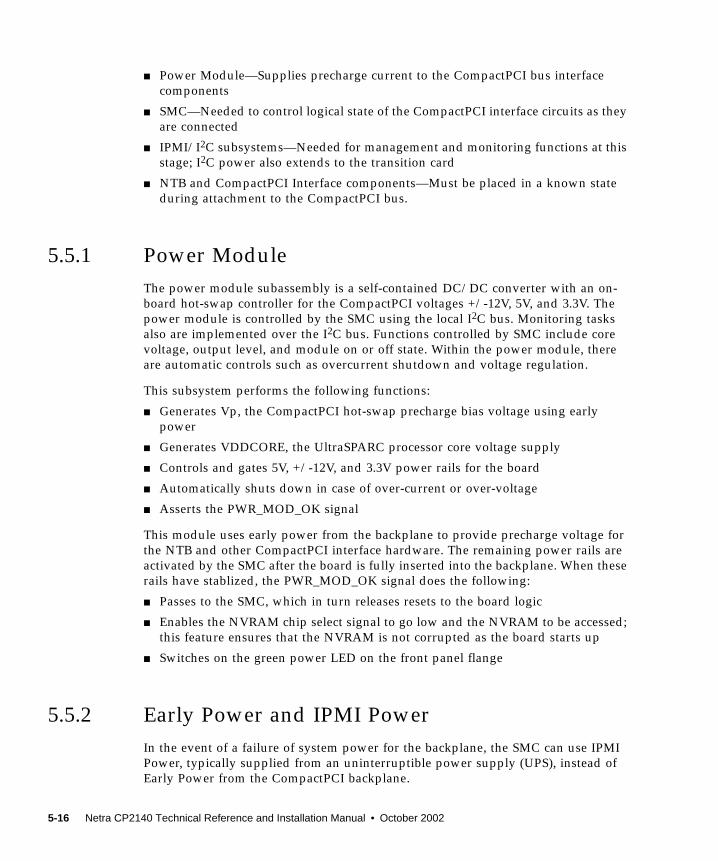
■ Power Module—Supplies precharge current to the CompactPCI bus interfacecomponents
■ SMC—Needed to control logical state of the CompactPCI interface circuits as theyare connected
■ IPMI/I2C subsystems—Needed for management and monitoring functions at thisstage; I2C power also extends to the transition card
■ NTB and CompactPCI Interface components—Must be placed in a known stateduring attachment to the CompactPCI bus.
5.5.1 Power ModuleThe power module subassembly is a self-contained DC/DC converter with an on-board hot-swap controller for the CompactPCI voltages +/-12V, 5V, and 3.3V. Thepower module is controlled by the SMC using the local I2C bus. Monitoring tasksalso are implemented over the I2C bus. Functions controlled by SMC include corevoltage, output level, and module on or off state. Within the power module, thereare automatic controls such as overcurrent shutdown and voltage regulation.
This subsystem performs the following functions:
■ Generates Vp, the CompactPCI hot-swap precharge bias voltage using earlypower
■ Generates VDDCORE, the UltraSPARC processor core voltage supply
■ Controls and gates 5V, +/-12V, and 3.3V power rails for the board
■ Automatically shuts down in case of over-current or over-voltage
■ Asserts the PWR_MOD_OK signal
This module uses early power from the backplane to provide precharge voltage forthe NTB and other CompactPCI interface hardware. The remaining power rails areactivated by the SMC after the board is fully inserted into the backplane. When theserails have stablized, the PWR_MOD_OK signal does the following:
■ Passes to the SMC, which in turn releases resets to the board logic
■ Enables the NVRAM chip select signal to go low and the NVRAM to be accessed;this feature ensures that the NVRAM is not corrupted as the board starts up
■ Switches on the green power LED on the front panel flange
5.5.2 Early Power and IPMI PowerIn the event of a failure of system power for the backplane, the SMC can use IPMIPower, typically supplied from an uninterruptible power supply (UPS), instead ofEarly Power from the CompactPCI backplane.
5-16 Netra CP2140 Technical Reference and Installation Manual • October 2002
FIGURE 5-10 shows the circuit arrangement that selects between these power sources.
FIGURE 5-10 Selection Between Early Power and IPMI Power
The comparator monitors Early Power and IPMI Power and enables one of thecurrent limiters—based upon MOSFET switches—at a time. When Early Powervoltage drops below specification, its supply to the board is disabled and the IPMIPower MOSFET switch is turned on, passing that supply to the load instead.Restoration of Early Power returns the switches to their original states.
5.6 Hot SwapThis section provides hot-swap architecture information and a description of thedifferent hot-swap models.
In general, hot swapping is the capability or property of a system element to beremoved or replaced while the system hardware is nominally operating underpower. The objectives in introducing hot-swap capability to a CompactPCI systeminclude the following:
■ Enable the insertion and extraction of boards without adversely affecting systemoperation.
■ Provide programmatic access to hot-swap services to enable systemreconfiguration and fault recovery, with no down time and minimum operatorintervention.
■ For HA applications, hot swap enables the system to isolate faulty boards so thata system can continue operations in the event of failure.
There are three levels of hot swap:
CURRENTLIMITER EN
EN
SMC Power
CURRENTLIMITER
COMPARATOR SMC
Early Power
IPMI Power
Chapter 5 Functional Description 5-17

Basic: Provides hardware features required to perform hot swap, but operatorintervention is required to execute software steps such as system configuration andinstallation of device drivers.
Full Hot Swap: Provides both hardware and software features required for softwareconnection control. Board software connection control resources provide thefollowing:
■ ENUM# signal to indicate service requests to the system host, which includeadding or removing software drivers for boards that have been inserted orextracted.
■ Hot swap switch: to indicate an operator wishes to extract a board
■ Blue LED: which is illuminated to indicate that it is safe to extract a boardwithout interrupting system operation.
High Availability (HA): In an HA system, hardware and software is added to enable ahigher degree of system control. The following signals are issued to control each slotin the system:
■ BD_SEL#: One of the shortest pins on a system backplane - this pin is the last tomate and the first to break contact. This ensures that sensing takes place at a timewhen all other pins are reliably connected.
■ Healthy#: A radial signal that signals a board is suitable to be released from resetand enabled onto the PCI bus.
■ PCI_RST#: Driven by the system host, platforms can use this signal to control theelectrical connection process - boards cannot come out of reset until Healthy#signal is indicated.
5.7 Programmable Logic Device(PLD)/ArbiterThe arbiter in the PLD provides arbitration of the CompactPCI bus interface withSMC optional boot flash PROM interfaces. As a system controller, the arbiterreceives seven requests from the CompactPCI bus and one request from the NTB.The arbiter processes the eight requests based on a round-robin arbitration scheme.As a satellite, the arbiter is disabled and the system passes the NTB request toCompactPCI request 0 and passes CompactPCI grant 0 to 21555 request.
5-18 Netra CP2140 Technical Reference and Installation Manual • October 2002

CHAPTER 6
Firmware
This chapter describes the structure and function of initialization firmware. TheNetra CP2140 board platform comprises a modular firmware architecture thatenables the user to customize initialization and test firmware, even enabling theinstallation of a custom operating environment.
The SPARC firmware consists of two components: Common Operations and ResetEnvironment (CORE) and OpenBoot PROM. The CORE in its expanded form isCommon Operations and Reset Environment. CORE handles the early initializationof the board before the SPARC control is transferred to OpenBoot PROM. It alsoprovides a trap-based interface for the OpenBoot PROM and user firmware.
This platform also employs the System Management Controller (SMC). The SMCcontrols the CompactPCI interface, System Management and hot-swap control, andsome board hardware. The SMC configuration is controlled by separate firmware.
6.1 Initialization FirmwareThe control flow at board startup is shown in FIGURE 6-1. Execution begins inFirmware CORE, which includes Basic POST (BPOST). Then it passes toComprehensive POST (CPOST) and Extended POST (EPOST), if these are present,before returning to Firmware CORE and on to OpenBoot PROM.
6-1

FIGURE 6-1 Control Flow from Power On for Firmware CORE and ClientModules—Solaris Case
6.1.1 Firmware CORE and BPOSTFirmware CORE:
■ Unifies system initialization and I/O operations for a higher level client, forexample, OpenBoot PROM for Solaris software
■ Avoids any duplication of effort for the same type of functions among variousclients
■ Provides a unified interface to higher level software using a soft-trap mechanism.Trap services (software interrupts) are used to abstract hardware-dependentfeatures behind a uniform service interface. Sun SPARC processors are designedwith a common software trap structure that is useful for this commonprogramming interface, so that clients do not need to carry another copy of thosedrivers and can use those services provided by Firmware CORE until theirdrivers take over.
■ Provides access, early in the boot sequence, to the hardware-dependent servicesneeded for client initialization; examples are I/O devices including serial port,flash, floppy, and net.
■ Provides basic system tests that can replace existing POST in min mode
■ Enables extensive system testing using the POST drop in max mode
CPOSTExtended
POST
OpenBootPROM
Other O/S
Solaris SunVTS
Power ON Reset
Control Flow from Power ON Reset
Return to Firmware CORE
Trap-basedInterface
COREFirmware
& BPOST
6-2 Netra CP2140 Technical Reference and Installation Manual • October 2002

■ Provides error recovery from exceptions which currently does not exist inOpenBoot PROM
■ Enables use of popular languages with efficient compilation and easier debuggingfor development
See Section 6.10, “Firmware Diagnostics” on page 6-38 for detailed information.
BPOST is integrated into Firmware CORE. Its tests are interleaved with theinitialization activities of Firmware CORE to present a foundation of validated andinitialized hardware to run subsequent code such as that in CPOST or OpenBootPROM. The tests listed in TABLE 6-1 are examples of CORE and BPOST flow ofexecution.
Note – Not all of the hardware listed in this table is present on this platform. If ahardware item is not detected by the firmware, the firmware makes no attempt totest or initialize it.
Because BPOST runs from PROM, the extent of testing is limited to that needed bymodules that are loaded later. Such a module, for example CPOST, can performcomprehensive testing more quickly because it executes from DRAM.
TABLE 6-1 Firmware CORE and BPOST Flow of Execution
Firmware CORE Service Detail
Initialize Processor Set processor in stable state
Initialize NVRAM Set up state variables
Initialize EBus andbridges
Initialize EBus and bridges in path between CPU and EBus devices
Initialize Super I/O, TTY For keyboard/mouse, message display, floppy
Set memory timings
Verify NVRAM Check magic number. Set defaults if invalid
Check keyboard Probe and initialize keyboard, set TTYA otherwise
Check I/P device for keypressed
Set state variables in NVRAM accordingly
Cache, MMU test Perform basic diagnostics on caches and MMUs*
Initialize caches, MMUs Set up I and D caches and MMUs
Memory test Perform partial memory test†
Memory probe Probe memory and clear top memory region
MMU and cache setup Set up I/D MMUs with valid mappings; enable MMUs and I/Dcaches
Chapter 6 Firmware 6-3

6.1.2 CPOST and EPOSTCPOST contains tests for higher level board functions. By placing these tests in aseparate module, the user has the option of performing them and the developer cansubstitute them with other tests. Examples of CPOST tests are:
■ PBM, IOMMU, APB, tests■ PCI Tests■ PCIO-2 Tests■ SCSI controller tests■ SMC diagnostic tests■ Memory stress tests
EPOST is used for additional POST code dropins that are provided by the user.
6.1.3 OpenBootPROM
Note – Always upgrade board OpenBoot PROM before upgrading SMC (SystemManagement Controller) firmware.
Copy Firmware CORE Copy Firmware CORE into memory and transfer control to theRAM copy
Set up trap table Set up trap table in memory
Initialize interrupts Set up hardware interrupts
Probe flash PROMs Probe for type and size of flash PROMs in the system
Initialize TOD
Set up CPU counter Calibrate CPU counter to determine module speed
Probe PCI bus Probe for Primary PCI system bus
Execute POST dropin†
Locate the client Locate the client in PROM. If found, copy into memory and transfercontrol to it
Enter user interface OpenBoot PROM for Solaris software, else RTOS or custom OS
* Execute if hardware power-on, run-post set to true, post-level set to min/max, and key to skip post not pressed.
† Execute if hardware power-on, run-post set to true, post-level set to max, and key to skip post not pressed.
TABLE 6-1 Firmware CORE and BPOST Flow of Execution (Continued)
Firmware CORE Service Detail
6-4 Netra CP2140 Technical Reference and Installation Manual • October 2002
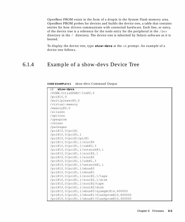
OpenBoot PROM exists in the form of a dropin in the System Flash memory area.OpenBoot PROM probes for devices and builds the device tree, a table that containsentries for how drivers communicate with connected hardware. Each line, or entry,of the device tree is a reference for the node entry for the peripheral in the /devdirectory in the / directory. The device tree is inherited by Solaris software as it isbooted.
To display the device tree, type show-devs at the ok prompt. An example of adevice tree follows.
6.1.4 Example of a show-devs Device Tree
CODE EXAMPLE 6-1 show-devs Command Output
ok show-devs/SUNW,UltraSPARC-IIe@0,0/pci@1f,0/multiplexer@0,0/virtual-memory/memory@0,0/aliases/options/openprom/chosen/packages/pci@1f,0/pci@1/pci@1f,0/pci@1,1/pci@1f,0/pci@1/pci@1/pci@1f,0/pci@1,1/scsi@4/pci@1f,0/pci@1,1/usb@3,3/pci@1f,0/pci@1,1/network@3,1/pci@1f,0/pci@1,1/scsi@2,1/pci@1f,0/pci@1,1/scsi@2/pci@1f,0/pci@1,1/usb@1,3/pci@1f,0/pci@1,1/network@1,1/pci@1f,0/pci@1,1/ebus@3/pci@1f,0/pci@1,1/ebus@1/pci@1f,0/pci@1,1/scsi@2,1/tape/pci@1f,0/pci@1,1/scsi@2,1/disk/pci@1f,0/pci@1,1/scsi@2/tape/pci@1f,0/pci@1,1/scsi@2/disk/pci@1f,0/pci@1,1/ebus@3/sysmgmt@14,600000/pci@1f,0/pci@1,1/ebus@1/flashprom@10,800000/pci@1f,0/pci@1,1/ebus@1/flashprom@10,400000
Chapter 6 Firmware 6-5
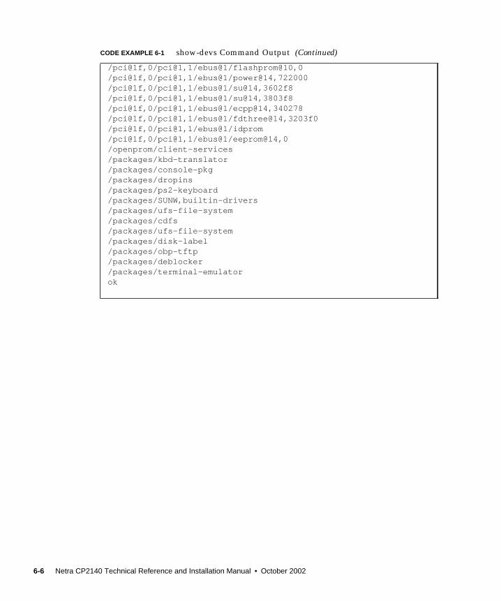
/pci@1f,0/pci@1,1/ebus@1/flashprom@10,0/pci@1f,0/pci@1,1/ebus@1/power@14,722000/pci@1f,0/pci@1,1/ebus@1/su@14,3602f8/pci@1f,0/pci@1,1/ebus@1/su@14,3803f8/pci@1f,0/pci@1,1/ebus@1/ecpp@14,340278/pci@1f,0/pci@1,1/ebus@1/fdthree@14,3203f0/pci@1f,0/pci@1,1/ebus@1/idprom/pci@1f,0/pci@1,1/ebus@1/eeprom@14,0/openprom/client-services/packages/kbd-translator/packages/console-pkg/packages/dropins/packages/ps2-keyboard/packages/SUNW,builtin-drivers/packages/ufs-file-system/packages/cdfs/packages/ufs-file-system/packages/disk-label/packages/obp-tftp/packages/deblocker/packages/terminal-emulatorok
CODE EXAMPLE 6-1 show-devs Command Output (Continued)
6-6 Netra CP2140 Technical Reference and Installation Manual • October 2002

OpenBoot PROM also contains aliases for some of the devices shown in the devicetree. These aliases can simplify hardware access at the ok prompt, for example:
ok boot disk1
The devalias command lists the device tree aliases. An example of the devaliascommand follows.
6.1.5 Example of devalias Command
CODE EXAMPLE 6-2 devalias Command Output
ok devaliasuserprom2/pci@1f,0/pci@1,1/ebus@1/flashprom@10,800000userprom1/pci@1f,0/pci@1,1/ebus@1/flashprom@10,400000systemprom /pci@1f,0/pci@1,1/ebus@1/flashprom@10,0output-mux /multiplexer:outputinput-mux /multiplexer:inputdload /pci@1f,0/pci@1,1/network@1,1:,hsc /pci@1f,0/pci@1,1/ebus@3/sysmgmt@14,600000pcic /pci@1f,0/pci@1/pci@1pcib /pci@1f,0/pci@1,1pcia /pci@1f,0/pci@1ebus2 /pci@1f,0/pci@1,1/ebus@3ebus /pci@1f,0/pci@1,1/ebus@1net2 /pci@1f,0/pci@1,1/network@3,1net /pci@1f,0/pci@1,1/network@1,1floppy /pci@1f,0/pci@1,1/ebus@1/fdthreediskx /pci@1f,0/pci@1,1/scsi@2,1/disk@0,0cdromx /pci@1f,0/pci@1,1/scsi@2,1/disk@6,0:ftapex /pci@1f,0/pci@1,1/scsi@2,1/tape@4,0tapex1 /pci@1f,0/pci@1,1/scsi@2,1/tape@5,0tapex0 /pci@1f,0/pci@1,1/scsi@2,1/tape@4,0diskxf /pci@1f,0/pci@1,1/scsi@2,1/disk@f,0diskxe /pci@1f,0/pci@1,1/scsi@2,1/disk@e,0diskxd /pci@1f,0/pci@1,1/scsi@2,1/disk@d,0diskxc /pci@1f,0/pci@1,1/scsi@2,1/disk@c,0diskxb /pci@1f,0/pci@1,1/scsi@2,1/disk@b,0diskxa /pci@1f,0/pci@1,1/scsi@2,1/disk@a,0diskx9 /pci@1f,0/pci@1,1/scsi@2,1/disk@9,0diskx8 /pci@1f,0/pci@1,1/scsi@2,1/disk@8,0diskx7 /pci@1f,0/pci@1,1/scsi@2,1/disk@7,0diskx6 /pci@1f,0/pci@1,1/scsi@2,1/disk@6,0
Chapter 6 Firmware 6-7

diskx5 /pci@1f,0/pci@1,1/scsi@2,1/disk@5,0diskx4 /pci@1f,0/pci@1,1/scsi@2,1/disk@4,0diskx3 /pci@1f,0/pci@1,1/scsi@2,1/disk@3,0diskx2 /pci@1f,0/pci@1,1/scsi@2,1/disk@2,0diskx1 /pci@1f,0/pci@1,1/scsi@2,1/disk@1,0diskx0 /pci@1f,0/pci@1,1/scsi@2,1/disk@0,0scsix /pci@1f,0/pci@1,1/scsi@2,1disk /pci@1f,0/pci@1,1/scsi@2/disk@0,0cdrom /pci@1f,0/pci@1,1/scsi@2/disk@6,0:ftape /pci@1f,0/pci@1,1/scsi@2/tape@4,0tape1 /pci@1f,0/pci@1,1/scsi@2/tape@5,0tape0 /pci@1f,0/pci@1,1/scsi@2/tape@4,0diskf /pci@1f,0/pci@1,1/scsi@2/disk@f,0diske /pci@1f,0/pci@1,1/scsi@2/disk@e,0diskd /pci@1f,0/pci@1,1/scsi@2/disk@d,0diskc /pci@1f,0/pci@1,1/scsi@2/disk@c,0diskb /pci@1f,0/pci@1,1/scsi@2/disk@b,0diska /pci@1f,0/pci@1,1/scsi@2/disk@a,0disk9 /pci@1f,0/pci@1,1/scsi@2/disk@9,0disk8 /pci@1f,0/pci@1,1/scsi@2/disk@8,0disk7 /pci@1f,0/pci@1,1/scsi@2/disk@7,0disk6 /pci@1f,0/pci@1,1/scsi@2/disk@6,0disk5 /pci@1f,0/pci@1,1/scsi@2/disk@5,0disk4 /pci@1f,0/pci@1,1/scsi@2/disk@4,0disk3 /pci@1f,0/pci@1,1/scsi@2/disk@3,0disk2 /pci@1f,0/pci@1,1/scsi@2/disk@2,0disk1 /pci@1f,0/pci@1,1/scsi@2/disk@1,0disk0 /pci@1f,0/pci@1,1/scsi@2/disk@0,0scsi /pci@1f,0/pci@1,1/scsi@2ttyb /pci@1f,0/pci@1,1/ebus@1/su@14,3602f8ttya /pci@1f,0/pci@1,1/ebus@1/su@14,3803f8ok
CODE EXAMPLE 6-2 devalias Command Output (Continued)
6-8 Netra CP2140 Technical Reference and Installation Manual • October 2002
6.2 Firmware NVRAM VariablesThis section provides some information on the CORE NVRAM variables and theNVRAM configuration variables.
6.2.1 Firmware CORE NVRAM VariablesAt startup, Firmware CORE defines a set of variables in the NVRAM for controllinginitialization and selecting the amount of testing required. These variables determinethe following functions:
■ run-post: If true, POST is executed depending upon the value of post-levelvariable. If false, POST is skipped.
■ post-level: Defines the level of diagnostics to be executed
■ msg-verbosity: If run-post is nonzero, msg-verbosity defines the level ofmessages displayed on TTY interface
■ user-interface: CORE falls into the user-interface without invoking the client
■ kernel: Name of the client to be loaded and executed by Firmware CORE
■ trap-state: Defines the behavior of an error trap
6.2.2 Firmware CORE Execution ControlUse the key combinations listed in TABLE 6-2 to control the flow of execution atsystem boot. These key combinations must be pressed at power-on.
TABLE 6-2 Firmware Execution Control Key Sequences
Key combination Result
Control-P Skip POST
Control-U Enter CORE user interface
Control-N Set default NVRAM variables
Control-M Turn on power on messages
Chapter 6 Firmware 6-9
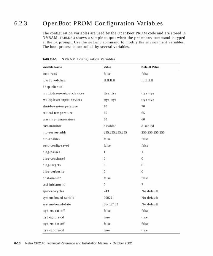
6.2.3 OpenBoot PROM Configuration VariablesThe configuration variables are used by the OpenBoot PROM code and are stored inNVRAM. TABLE 6-3 shows a sample output when the printenv command is typedat the ok prompt. Use the setenv command to modify the environment variables.The boot process is controlled by several variables.
TABLE 6-3 NVRAM Configuration Variables
Variable Name Value Default Value
auto-run? false false
ip-addr-obdiag ff.ff.ff.ff ff.ff.ff.ff
dhcp-clientid
multiplexer-output-devices ttya ttye ttya ttye
multiplexer-input-devices ttya ttye ttya ttye
shutdown-temperature 70 70
critical-temperature 65 65
warning-temperature 60 60
env-monitor disabled disabled
ntp-server-addr 255.255.255.255 255.255.255.255
ntp-enable? false false
auto-config-save? false false
diag-passes 1 1
diag-continue? 0 0
diag-targets 0 0
diag-verbosity 0 0
post-on-sir? false false
scsi-initiator-id 7 7
#power-cycles 743 No default
system-board-serial# 000221 No default
system-board-date 06/12/02 No default
ttyb-rts-dtr-off false false
ttyb-ignore-cd true true
ttya-rts-dtr-off false false
ttya-ignore-cd true true
6-10 Netra CP2140 Technical Reference and Installation Manual • October 2002

ttyb-mode 9600,8,n,1,- 9600,8,n,1,-
ttya-mode 9600,8,n,1,- 9600,8,n,1,-
cpci-probe-list 0,1,2,3,4,5,6,7,8,9,a,b,.. 0,1,2,3,4,5,6,7,8,9,a,b,...
pcia-probe-list 1 1
pcib-probe-list 1,2,3,4 1,2,3,4
probe-delay 30 30
keyboard-click? false false
keymap
mfg-mode off off
diag-level max max
watchdog-timeout 65535 65535
watchdog-enable? false false
fcode-debug? false false
output-device screen screen
input-device keyboard keyboard
load-base 16384 16384
auto-boot-retry? false false
boot-command boot boot
auto-boot? true true
watchdog-reboot? false false
diag-file
diag-device net net
boot-file
boot-device disk net disk net
net-timeout 0 0
ansi-terminal? true true
screen-#columns 80 80
screen-#rows 34 34
local-mac-address? false false
silent-mode? false false
TABLE 6-3 NVRAM Configuration Variables (Continued)
Variable Name Value Default Value
Chapter 6 Firmware 6-11
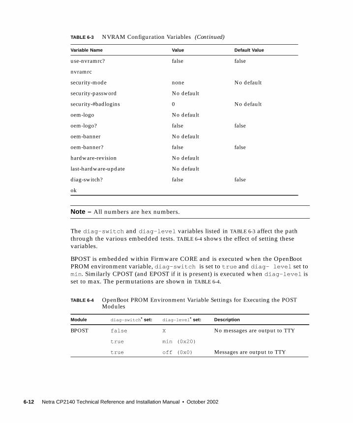
Note – All numbers are hex numbers.
The diag-switch and diag-level variables listed in TABLE 6-3 affect the paththrough the various embedded tests. TABLE 6-4 shows the effect of setting thesevariables.
BPOST is embedded within Firmware CORE and is executed when the OpenBootPROM environment variable, diag-switch is set to true and diag- level set tomin. Similarly CPOST (and EPOST if it is present) is executed when diag-level isset to max. The permutations are shown in TABLE 6-4.
use-nvramrc? false false
nvramrc
security-mode none No default
security-password No default
security-#badlogins 0 No default
oem-logo No default
oem-logo? false false
oem-banner No default
oem-banner? false false
hardware-revision No default
last-hardware-update No default
diag-switch? false false
ok
TABLE 6-4 OpenBoot PROM Environment Variable Settings for Executing the POSTModules
Module diag-switch* set: diag-level* set: Description
BPOST false X No messages are output to TTY
true min (0x20)
true off (0x0) Messages are output to TTY
TABLE 6-3 NVRAM Configuration Variables (Continued)
Variable Name Value Default Value
6-12 Netra CP2140 Technical Reference and Installation Manual • October 2002

6.3 Firmware Memory MapThe host board boots from the 1 Mbyte system flash PROM device, which containsthe firmware CORE, Basic POST code, Comprehensive POST, and OpenBoot PROM.The contents map of this PROM is shown in FIGURE 6-2. User-developed code canalso be programmed into the user flash memory space in the form of dropins. Thesystem flash can be upgraded by running a program out of OpenBoot PROM—see“OpenBoot PROM Flash Update” on page 6-19. It is not otherwise accessible to theuser.
CPOST false X No messages are output to TTY
true max (0x40) Runs after BPOST
true off (0x0) Messages are output to TTY
EPOST false X No messages are output to TTY
true max (0x40) Runs automatically after CPOST(if EPOST module is present)
true off (0x0) Messages are output to TTY
* Firmware CORE variables run-post and post-level are equivalent to enviromnment variables diag-switch and diag-level respectively.
TABLE 6-4 OpenBoot PROM Environment Variable Settings for Executing the POSTModules
Module diag-switch* set: diag-level* set: Description
Chapter 6 Firmware 6-13

FIGURE 6-2 System Flash PROM Map
HeaderCORE0
Drop ins
0x20
HeaderName: FVM
HeaderName: Keyboard
HeaderName: cPOST
cPOST
Keyboard Drop In
Free Space
OpenBoot PROM/FVM
CORE
0x20
0x20
20
6-14 Netra CP2140 Technical Reference and Installation Manual • October 2002

6.4 Firmware CORE FeaturesTABLE 6-5 lists the firmware CORE commands that are run from the monitor.
TABLE 6-5 Firmware CORE Monitor Commands
Description of Task CORE Monitor Command
To get this help help
To allocate memory buffer malloc <size>
To free memory buffer free <addr>
To block copy memory bcopy <src> <dest> <#bytes>
To dump memory dump <addr> <#bytes> [asi]
To read an address [safe-]peek <addr> <1|2|4|8> [asi]
To write to an address poke <addr> <1|2|4|8> <data> [asi]
To update Flash PROM flash-update <dev> <file-path>
To load a file load <device> <file-path> <addr>
Jump to an address go <addr>
Execute client execute [client-name]
Print NVRAM data print-nvram
Write to NVRAM variable set-nvram <variable-name|ID> <data>
Read an NVRAM variable get-nvram <variable-name|ID>
Delete an NVRAM variable delete-nvram <ID>
Set NVRAM variables to default set-defaults
Call a trap function trap <trap#> <par0> ... <par5>
Soft Reset reset
To change input device input-device <tty|kbd>
To initialize PCI init-pci
To show all pci devices show-pci-devs
To show pci config space show-pci-space <bus#> <device#><function#> <offset>
To show pci nexus nodes show-nexus-nodes
To remove a pci device rm-pci-dev <device#>
To add a pci device add-pci-dev <device#>
Chapter 6 Firmware 6-15

Note – All numbers are hex numbers.
6.5 ASM SupportASM support is added at the OpenBoot PROM level. The ASM monitors the CPUtemperature. The CPU warning, critical and shutdown temperature default limitsare set at 60˚ C, 65˚ C and 70˚ C, respectively. For more information on ASMWarning, Critical and Shutdown temperature parameter settings, refer to the NetraCP2000 and CP2100 Series CompactPCI Boards Programming Guide for Solaris OperatingEnvironment (816-0854-xx).
The following NVRAM variables are added in OpenBoot PROM for ASM:
1) NVRAM variable name: env-monitor?
Function :enables or disables environment monitoring at OBP.
Data type :string
Valid values :disabled or enable
Default value :disable
OBP Usage :OK setenv env-monitor? enable
2) NVRAM variable name :warning-temperature
Function :sets the cpu warning temperature threshold
Data type :byte
Unit :Decimal
Default value :60
OBP Usage :ok setenv warning-temperature <temperature-value>
3) NVRAM variable name :shutdown-temperature
Function :sets the cpu shutdown temperature threshold
Data type :byte
Unit :Decimal
To remove all pci devices rm-pci-devs
To add all pci devices add-pci-devs
To execute UI cmd in loop loop <count> <command>
TABLE 6-5 Firmware CORE Monitor Commands (Continued)
Description of Task CORE Monitor Command
6-16 Netra CP2140 Technical Reference and Installation Manual • October 2002

Default value :70
OBP Usage :ok setenv shutdown-temperature <temperature-value>
CAUTION: User should exercise caution while setting the above two parameters.
Setting these values too high leaves the system un-protected against system
over-heat.
WARNING: Temperature response at OBP When cpu temperature reaches
"warning-temperature", the following message is spit out at ok prompt
at a regular interval:
.......
Temperature sensor #2 has threshold event of
<<< WARNING!!! Crossing Warning temperature threshold >>>
The current threshold setting is: 18
The current temperature is : 28
.......
Critical Temperature response at OBP
Sensor in IPMB Addr 20 has event ===
Temperature sensor #2 has threshold event of
<<< !!! ALERT!!! Crossing Critical temperature threshold >>>
The current threshold setting is: 20 degreeC
The current temperature is : 28 degreeC
Shutdown Temperature response at OBP
When cpu temperature reaches "warning-temperature", the following message isdisplayed at ok prompt at a regular interval,
...........
Temperature sensor #2 has threshold event of
<<< !!! ALERT!!! Upper Critical - going high >>>
The current threshold setting is: 65
The current temperature is : 66
...........
Chapter 6 Firmware 6-17

show-sensor command at OBP
--------------------------
The "show-sensor" command at OBP displays the readings of all the temperaturesensors on the board.
6.6 Determining Firmware VersionIf the installed version is not current, update the OpenBoot PROM beforecontinuing. The third character group (X) in OpenBoot PROM is the revisionnumber.
6.6.1 From OpenBoot PROMTo determine the installed OpenBoot PROM version, type the .version commandat the ok prompt. For an example, the firmware version in the output below is theOpenBoot PROM version:
6.6.2 If Running Solaris SoftwareType the prtconf command at the machine_name prompt:
ok .version
Firmware version 1.0.5
SMC Firmware Release 3.4.15 Platform ID 10
FPGA Version 1.0
PLD Version 1.3
Firmware CORE Release 1.0.5 created 2002/7/22 20:53
Release 4.0 Version 5 created 2002/07/29 19:09
cPOST version 1.0.3 created 2001/9/24
ok
machine_name% /usr/bin/prtconf -V
OBP 4.0.xx creation date
6-18 Netra CP2140 Technical Reference and Installation Manual • October 2002
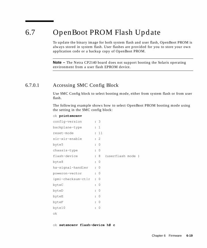
6.7 OpenBoot PROM Flash UpdateTo update the binary image for both system flash and user flash, OpenBoot PROM isalways stored in system flash. User flashes are provided for you to store your ownapplication code or a backup copy of OpenBoot PROM.
Note – The Netra CP2140 board does not support booting the Solaris operatingenvironment from a user flash EPROM device.
6.7.0.1 Accessing SMC Config Block
Use SMC Config block to select booting mode, either from system flash or from userflash.
The following example shows how to select OpenBoot PROM booting mode usingthe setting in the SMC config block:
ok printsmcenv
config-version : 3
backplane-type : 1
reset-mode : 11
sir-xir-enable : 2
byte5 : 0
chassis-type : 0
flash-device : 8 (userflash mode )
byte8 : 0
ha-signal-handler : 0
poweron-vector : 0
ipmi-checksum-ctlr : 0
byteC : 0
byteD : 0
byteE : 0
byteF : 0
byte10 : 0
ok
ok setsmcenv flash-device h# c
Chapter 6 Firmware 6-19

ok printsmcenv
config-version : 3
backplane-type : 1
reset-mode : 11
sir-xir-enable : 2
byte5 : 0
chassis-type : 0
flash-device : c (userflash mode c is equivalent
to sysflash mode)
byte8 : 0
ha-signal-handler : 0
poweron-vector : 0
ipmi-checksum-ctlr : 0
byteC : 0
byteD : 0
byteE : 0
byteF : 0
byte10 : 0
ok
6.7.0.2 Using Flash Update Commands
The command format is flash-update file-path flashtype.
ok flash-update file-path systemprom <---- to update system flash
ok flash-update file-path userprom1 <---- to update user flash1
ok flash-update file-path userprom2 <---- to update user flash2
In the absence of flashtype, the OpenBoot PROM updates OpenBoot PROM inwhatever flash has the address:
/pci@1f,0/pci@1,1/ebus@1/flashprom@10,0
For example, in sysflash mode, the system flash is updated. In the user flash mode,the user flash #1 is updated.
If a combined SPARC and SMC binary file is provided to the flash-updatecommand then it updates SMC as well as the SPARC firmware. Use the regularflash-update command to update the combined binary and follow the syntax ofthe flash-update command with the full file path of the combined binary.
6-20 Netra CP2140 Technical Reference and Installation Manual • October 2002

6.7.0.3 Field CORE/OpenBoot PROM Firmware Upgrade
This firmware can only be upgraded when operating at the OpenBoot PROM level,that is, at the ok prompt. The following procedure gives the steps to updatefirmware on the target system.
1. Download the latest Netra CP2140 board host firmware binaries.
Download the latest CP2140 host firmware (OpenBoot PROM) and SMC firmware toyour server. Contact your Field Application Engineer for help on how to downloadit.
2. Bring the system down to OpenBoot PROM level.
If your Netra CP2140 host is currently running Solaris software, become superuserand type the following command to halt the system:
$ shutdown -i0 -g0 -y
or
$ init 0
3. Check the firmware revision.
Check the current firmware revision on the target system by typing:
ok .version
See Section 6.6.1, “From OpenBoot PROM” on page 6-18 for an example of theoutput of this command.
The Platform ID identifies the board ID. For example, if ID = 10 indicates theCP2140.
For each release, there must be compatible revision numbers for other components.To get the correct combination, refer to the latest release notes.
4. Disable autoboot; then reset.
Disable autoboot and reset the system using the following commands:
ok setenv auto-boot? false
ok reset-all
The system is now reset.
5. Flash update your firmware.
ok flash-update obp-file-path/obp-latest-binary
ok smc-flash-update smc-file-path/smc-latest-binary
If you have the combined SPARC and SMC binary file then use the followingcommand:
Chapter 6 Firmware 6-21

ok flash-update obp-smc-file-path/obp-smc-combined-latest-binary
The system should automatically reset. If it does not, power cycle it.
6. Check the firmware revision.
Check the firmware revision by typing:
ok .version
The output appears as in the example in Step 3. Ensure that the version informationshows up as expected. If not, repeat Step 1 through Step 6.
7. Enable autobooting and reset the system.
Enable autobooting by typing:
ok setenv auto-boot? true
and reset the system to boot the Solaris software:
ok reset-all
Contact your service personnel if you have any problems.
Note – Solaris scripts are also available to upgrade core OpenBoot PROM firmware.
6.7.0.4 Sequence to Boot Up the Correct OpenBoot PROM Image
The following sequence enables you to boot up the correct OpenBoot PROM image.
1. You are logged in UserFlash Mode 8 with OpenBoot PROM image from UserFlash #1, which has the following setup in SMC config block:
ok printsmcenv
config-version : 3
backplane-type : 1
reset-mode : 11
sir-xir-enable : 2
byte5 : 0
chassis-type : 0
flash-device : 8
byte8 : 0
ha-signal-handler : 0
poweron-vector : 0
ipmi-checksum-ctlr : 0
byteC : 0
6-22 Netra CP2140 Technical Reference and Installation Manual • October 2002

byteD : 0
byteE : 0
byteF : 0
byte10 : 0
ok
2. Flash updates new OpenBoot PROM to system flash:
ok flash-update file-path systemprom
3. Change to system flash to boot up if you want to boot from it:
ok setsmcenv flash-device c
4. Power cycle the CP2140 system.
The new OpenBoot PROM boots up from the system flash.
Chapter 6 Firmware 6-23
6.7.1 SMC Firmware UpdateSMC firmware is updated only from the OpenBoot PROM level. Follow these stepsto update the SMC firmware:
1. Check with your Field Application Engineer.
2. Type the following command:
smc-flash-update filename
Note – The filename must be a valid binary or else the file cannot be read tocomplete the flash update.
3. If a power failure occurs, or an error message displays, or you notice that thesecond binary is an F, then the flash update has failed.
The following example shows the binary breakdown:
4. You must now perform a code recovery of the SMC flash update in order for thecode to work.
6.7.2 IPMI PacketThis section describes how to send and receive packets from one board to anotherboard using the IPMI protocol. First, you must know how to set the IPMB address ofeach board.
The following steps show you how to calculate the Geographical Address bits:
1. Read Geographical Address bits.
To get the Geographical Address (GA) bits, type the following command:smc-get-ga
2. If (GA != 0) then:
if (GA <= 9) then
ipmb_addr = 0xB0 + (GA - 1) * 2
else if (GA <= 30)
First binary Secondary binary Third binary
SMCFw version = xx Revision = 0xF Build = xx
6-24 Netra CP2140 Technical Reference and Installation Manual • October 2002

ipmb_addr = 0xC4 + (GA - 10) * 2
else
ipmb_addr = 0
else
ipmb_addr = 0
3. For SBC, IPMB address is always 0x20.
Note – Upon power up, the SMC sets up the IPMB address of the boardautomatically, but you need to provide the sender’s and receiver’s IPMB addressesproperly within the IPMI packet in order to get the communication to work.
Before sending the IPMI packet to the other board, you must set a bit in the globalenable register inside SMC.
Note – All examples shown in this section are performed at the CORE level.
To do this, send cmd 0x2F to the SMC (get_smc_global_enable).
It returns three bytes of data: The first byte is completion code, the other 2 bytes areglobal enable bits.
After you get the data, send the following packet to the SMC:command 0x2E (set_smc_global_enables):
All values are in hex:07 : Byte count
XX : Checksum
XX : Sequence number
18 : NetFN/LUN
2e : set_smc_global_enables
YY : Put back the first byte that you read earlier.
ZZ : Put back the 2nd byte that you read earlier, but modify bit 4 to 0.
Now you can send the IPMI packet through the send_message command. Youmust append this IPMI packet to the EBus packet header, plus the channel number,where 0 is IPMI channel, 1 is the interhost channel.
Chapter 6 Firmware 6-25
Here is the format:
LL: Byte count
CS: Checksum
SN: Sequence number
18: NetFN/LUN
34: send_message command
Plus:
00: Channel number, IPMI channel is 0, Interhost is 1.
Append the following IPMI packet to the header:
RA: Responder address, in this case this is the destination IPMBaddress.
NF: IPMI net function for the command that you want to send.
This MUST be shifted left by 2 bits, and ORed it with LUN, in this case we set it to 1.
CS: Checksum for the IPMI packet.
QA: Requester address. This is the IPMB address of the requester.
SN: Sequence number
CM: IPMI command
Here is the diagram:
After this command is sent to the SMC, you will receive a response packet from theSMC.
Note – This is not the IPMI response packet; this is the SMC response packetindicating that it received the command.
If the packet is received, the SMC responds with:
06: Byte count.
CS: Checksum.
SN: Sequence number
1C: Response NetFN number
EBus packet header Channel IPMI packet
LL CS SN 18 34 CH 0 or 1 Append IPMI packet here
6-26 Netra CP2140 Technical Reference and Installation Manual • October 2002

34: send_message command.
00: OK.
After you retrieve that packet, you can send command 0x33 (get_message) in thefollowing format
05: Byte count.
CS: Checksum.
SN: Sequence number
18: NetFN/LUN
33: get_message command
If the packet is received, the other board which is appended to the EBus packetheader, responds with:
LL: Byte count
CS: Checksum
SN: Sequence number
1C: Response NetFN number
33: get message command
00: OK.
The IPMI response packet is appended to the packet header listed above. Source anddestination IPMB addresses are exchanged in the response packet.
Note – In order to get the response packet from the other board properly with theget_message command, the sequence number expected must match the sequencenumber sent.
Here is an example of the get_device_id command:
The packet looks like:
Send packet to read global enable bits
5 0 0 18 2f
You get the following response packet from the SMC:
8 0 0 1c 2f 0 0 14
Send packet to set global enable bits:
7 0 0 18 2e 0 4
Now you can send the IPMI packet to the other board so that it can read its deviceID.
c 0 22 18 34 0 b6 19 0 20 22 1 bd
Chapter 6 Firmware 6-27

The sequence number in this case is set to 22 (this number is picked arbitrarily).
Net function for get_device_id command is 6, and we shift it 2 bits to the left,and ORed it with logical unit number 1. Therefore it becomes 19. The b6 is theaddress of the board from which the device ID is requested.
Since this packet is being sent from the SBC, 20 is put as the requester IPMB addressand 1 is the get_device_id command for Netfunction 6 (Application).
If everything goes well, SMC sends the following response packet first:
6 0 22 1c 34 0
You can read the device ID packet of the other board, by issuing a get_messagecommand, the packet looks like this:
5 0 22 18 33
If the data is not available, the following response packet is received from the SMC:
6 0 22 1c 33 80
Completion code 80 indicates that data is not available.
Otherwise, you will get the following response packet from the SMC:
1d 0 22 1c 33 0 ......
followed by the IPMI response packet from the other board, with the requester andresponder addresses swapped from the original IPMI packet header.
TABLE 6-6 shows an example of a chassis configuration.
Note – On the first slot, the SBC is assigned an IPMB address of 0x20, not 0xB0. Ifthe second slot becomes SBC, then the IPMB address becomes 0x20, not 0xB2.
To send an IPMI packet to other boards, make sure that you include the correctchecksum data in the IPMI packet.
TABLE 6-6 Chassis Configuration Example
Slot 1 2 3 4 5 6 7 8
Geographical Address 1 2 3 4 5 X X x
IPMB Address 20 B2 B4 B6 B8 BA BC BE
6-28 Netra CP2140 Technical Reference and Installation Manual • October 2002

TABLE 6-7 shows what an IPMI packet looks like.
Check 1: This is the 2’s complement check sum of rsSA and netFn.
Check 2: This is the 2’s complement check sum of data starting from rqSA all the way to NN - 1 data.
To calculate the checksum, add all the data involved for that particular checksumentry, then use this formula:
checksum = - checksum
The checksum arithmetic that is done is module 256 since only one byte is allocatedfor each checksum. By performing this calculation, once all the data entries for thechecksum have been added and the result is added to that checksum, you get aresult of 0.
The examples below show how to send a packet at the OpenBoot PROM interface atthe ok prompt. At the OpenBoot PROM level, you do not have to include all EBuspacket header data, making the process simple.
Type the following commands at the ok prompt as shown below:
ok dev hsc
ok showstack
ok words
The showstack command enables you to see the value of the returned data. Thewords command lists all the commands that are supported.
Now you are ready to send the packets.
TABLE 6-7 IPMI Packet
Offset Data
00 rsSA
01 netFn
02 Check 1
03 rqSA
04 reSeq / rqLUN
05 cmd
06 (data)
.. ......
.. ......
NN - 1 .....
NN Check 2
Chapter 6 Firmware 6-29

The generic format is as follows:
ok ipmi_packet CH BC 34 execute-smc-cmd
Reviewers: Is ipmi_packet CH BC supposed to be variables and 34 execute-smc-cmdthe literal command?
Where the ipmi_packet is the data in the IPMI packet, CH is the channel numberand BC is the byte count.
Note – The IPMI packet data is entered backwards at the ok prompt.
In this example, the get_device_id_command is used. B6 is the destinationaddress or the responder, and 20 is the source address, or the requester. Thecommand for get_device_id is 1 and the NetFn data field in this case is 19 (after ithas been adjusted/shifted 2 bits to the left and ORed with 1). The sequence numberis set to 22 in this case.
The IMPI packet looks like this:
b6 19 0 20 22 1 > byte count = 6
The channel number is 0 indicating that this is an IPMI channel.
The total byte count is 6 + 1 (the channel number) = 7.
Type the command as follows:
ok 1 22 20 0 19 b6 0 7 34 execute-smc-cmd
if everything works as planned, you get the following message:
0 ok
At this point, you can issue a clear command to clear the stack.
You see the following message:
0 ok clear
ok
Now you are ready to issue command 33 to retrieve the response packet from theother board.
Type the following command:
ok 0 33 execute-smc-cmd
If everything works as planned, you receive the following message:
.....ipmi_response_packet....ok
You also receive the EBus response data appended to the ipmi_response_packet. Inthis case, it is 0.
6-30 Netra CP2140 Technical Reference and Installation Manual • October 2002

6.8 Host-to-Host CommunicationAn event is a packet of information in a fixed format which is sent by the SMC onone board to another board through IPMI. The events are usually generated by theSMC and they go to another board’s SMC, which sends it to the local SPARC.
But the event can also be generated by the SPARC wherein it sends the event packetto its SMC which sends the packet to another board. FIGURE 6-3 shows the host-to-host communication.
FIGURE 6-3 Host-to-Host Communication
Board 1
SMC sending event to SPARC on another board
SPARC sending event to SPARC on another board
SPARC
SMC
cmd88
IPMI
Board 2
SPARC
SMC
Board 1
SPARC
SMC
cmd88
IPMI
Board 2
SPARC
SMC
Chapter 6 Firmware 6-31
6.8.1 PacketThere is a fixed packet for any event to be sent. That packet is as follows:
evm_rev // Revision number
sensor_type
sensor_number
event_type_dir // dir => assertion/deasserion event..
event_data1
event_data2
event_data3
The packet formation depends on the sensor class and value. For example, if there isa temperature sensor, where the monitor task detects the temperature value higherthan the threshold value, the packet might look like the following:
evm_rev = 0x03; // for current specs it is 0x03
sensor_type = TEMPERATURE_SENSOR; // sensor 0x01,Table 30.3
sensor_number = 0xe; // Sensor # assigned to a sensor.
event_type_dir = 0x01; // implies Threshold based sensor,Table 30.1
event_data1 = 0x59; // Implies that in event_data2 we have
// current temp value and in event_data3 we
// have threhold value which triggered the
// event. see table 17.5 IPMI specs
event_data2 = temp_sensor_ds1721.temp; // current temp value.
event_data3 = temp_sensor_ds1721.high_temp; // threshold value.
Thus, the values specified in the variables change depending upon the event type.
For detailed explanation of these variables, refer to IPMI Intelligent PlatformManagement Interface Specification (A00328-xxx).
6-32 Netra CP2140 Technical Reference and Installation Manual • October 2002

6.8.2 Event ReceiverAll events are sent to the current event receiver. An event receiver is the address ofthe board which is bound to receive the events. By default, the event receiver is theBMC address 20 for all the SAT boards. However, any board can set itself or anyother board as event receiver for other boards.
For example, a board at address 0xb6 can send IPMI commandset_event_receiver to a board at address 0xba asking it to set address 0xb2 as itsevent receiver, so that now all the events from satellite at address 0xba goes toaddress b2. Similarly, the board at address 0xb6 could have asked 0xba to set 0xb6itself as event receiver (which usually is the case).
The SMC sends the event to the currently set event receiver, without verifyingwhether that address is set correctly or not.
6.8.3 ProtocolThe event generation follows a particular protocol as described in the following test.As soon as an event condition is detected, the SMC creates the packet to be sent andsends an event packet to the event receiver. It then waits for the response from theevent receiver to come until it times out. If the response does not come within thattime, it sends the event packet again, with a different sequence number and againwaits for the time out. This continues until retry count is exhausted.
During all this time, the state system is held in a state which indicates that the eventis transmitted and no response has been received. So, if during this period, anotherevent condition is generated, the event shall not be sent until the response topreviously sent event has timed out.
The state changes to normal idle state if either it times out or a response to the eventis received.
Refer to the IPMI Intelligent Platform Management Interface Specification (A00328-xxx)for more details.
When an event receiver gets an event packet, it does two things: First, it updates itsmini system event log where it keeps the latest event from the SAT which is sendingthe event; second, it sends the event packet to the local SPARC as an asynchronousmessage through command 0x88.
Chapter 6 Firmware 6-33

6.8.4 Generating an Event From SPARC to Send toAnother SPARCThis is a special case of event generation. Here the event is not sent to the currentevent receiver but to the address where the SPARC wants the event to be sent.
To send an event packet to another SPARC, the SPARC sends the packet throughEBus command send event (command f6) to the local SMC. Also it sends the addresswhere the event is to be sent. SMC extracts the packet and sends the event to thisaddress.
The protocol to send the event to the receiver address remains the same. When thereceiver gets the event packet, it sends the packet to local SPARC through command0x88.
The EBus packet for command 0xf6 looks similar to CODE EXAMPLE 6-3:
The response packet for this EBus command is as shown in CODE EXAMPLE 6-4:
CODE EXAMPLE 6-3 EBus Packet for Command 0xf6
LEN D
CHK 0
SEQ Sequence Number
NETFN/RSLUN 0X18
CMD 0XF6
IPMB ADDR
EVM REV
SENSOR TYPE
SENSOR NUMBER
EVENT DIR
EVENT DATA1
EVENT DATA2
EVENT DATA3
CODE EXAMPLE 6-4 Response Packet for EBus Command 0xf6
LEN 5
CHK 0
SEQ Sequence number
NETFN/RSLUN 0X1c
CMD 0XF6
CC Completion Code
6-34 Netra CP2140 Technical Reference and Installation Manual • October 2002
If the completion code is 0xC0, the SMC is waiting for the response to the previouslysent event packet. If the completion code is 0, the event packet has been sent.
6.9 SMC Implementation NoteThis document lists the features supported by this release (Release 3.8.9). A briefdescription is included for each command.
The list is sorted by the opcode number:
1. Cmd. 0x22, reset watchdog timer.
This is used to start and restart local watchdog.
2. Cmd. 0x24, set watchdog timer.
This is used to initialize and configure local watchdog timer.
3. Cmd. 0x25, get watchdog timer.
This is used to get the current setting and present countdown value.
4. Cmd. 0x2e, set SMC global enables.
This is used to set the global enable bits.
5. Cmd. 0x2f, get SMC global enables.
This is used to read the global enable bits settings.
6. Cmd. 0x33, get message.
This is used to retrieve data in the Receive Message Queue (RMQ). The data inRMQ is typically from IPMI channel.
7. Cmd. 0x34, send message.
This is used to send IPMI packet to the other board. The packet is appended tothe EBus packet, with the channel number.
8. Cmd. 0x52, master write-read I2C
This is used to communicate with devices via I2C channel. It is normally used forraw data communication, not like IPMI packet.
9. Cmd. 0x55, get geographical address.
This reads 5 bits of geographical address of the slot from the backplane.
10. Cmd. 0x60, select memory device.
Chapter 6 Firmware 6-35
This command is reserved for SMC flash update operations, therefore it can’t beused for other purposes. It selects the device type and segment number.
11. Cmd. 0x63, write selected memory device.
This command is reserved for SMC flash update operations. It writes multiplebytes of data into the selected device.
12. Cmd. 0x65, erase selected memory device.
This command is also reserved for SMC flash update operations. It erases onesegment of the selected device.
13. Cmd. 0x6f, get firmware version.
This command returns multiple bytes of data, which includes version number,and if the code is running from main flash or boot flash. It also tells if the code isfor actual production or testing.
14. Cmd. 0x70, reset device.
This command is used to reset device, and to control the level of reset (max ormin. reset).
15. Cmd. 0x71, get role information.
This is used to find out if the board is SBC, SSBC or SAT.
16. Cmd. 0x83, notify SMC of host health.
This is used by SPARC to notify SMC of its health status.It updates the SMC theexecution state of the host. Useful for power up sequence.
17. Cmd. 0x84, turn blue, or red LED on/off.
This is used to control the blue LED on the front panel of the board.
18. Cmd. 0x87, enum notification.
This is an asynchronous message sent by the SMC to the host. It is used to notifythe host of a pending ENUM condition.
Note – The host does not send this command. This is an asynchronous commandwhich means it comes only from the SMC.
19. Cmd. 0x88, IPMI response message notification.
This command is used by SMC to send unsolicited data to the host.
Note – The host does not send this command. This is an asynchronous commandwhich means it comes only from the SMC.
6-36 Netra CP2140 Technical Reference and Installation Manual • October 2002
20. Cmd. 0x8b, SMC local event.
This is used by the SMC to update the host of the action taken by the SMC. It isnormally used during power up/reset.
Note – This is also an asynchronous command, only sent by the SMC.
21. Cmd. 0x8c, get device table data.
This is used by the host to read device table information. The device table containsdata of which slots are occupied, etc. Only the board that support IPMI is listed.
22. Cmd. 0xa0, get SMC self test results.
This is used to read the SMC self test results. The self tests are done at power uponly.
23. Cmd. 0xc3, EEPROM write.
This command is used to write data into I2C EEPROM devices using I2C channel(Channel 2). Multiple data can be written in one pass.
24. Cmd. 0xc4, EEPROM read.
This command is used to read data from EEPROM devices, using I2C channel(Channel 2). Multiple data can be read in one pass.
25. Cmd. 0xf4, get sensor event enable. This command is used to get the sensor eventenable setting.
26. Cmd. 0xf5, set sensor event enable.
This is used to enable or disable sensor event generator. Each sensor eventgenerator can be enabled or disabled
27. Cmd. 0xf6, send event.
This is used by one host to communicate with the other host on another board indifferent slot.
28. Cmd. 0xf8, get configuration block.
This is used to read the configuration data in the I2C EEPROM device.
29. Cmd. 0xf9, set configuration block.
This command is used to set the configuration data in the I2C EEPROM device.
The data is used for power up sequence.
Chapter 6 Firmware 6-37

Note – In order to take effect, after the new data is written, the board must bepower cycled.
30. Cmd. 0xfb, set voltage.
This is used to set voltage level in the power module. Please consult the hardwareteam before using this command for testing.
31. Cmd. 0xfc, get sensor reading.
This is used to read the data of selected sensor. The data read includes the currentstatus with respect to the threshold value, or state value.
32. Cmd. 0xfd, get sensor threshold
This command is used to get the current sensor threshold settings.
33. Cmd. 0xfe, set sensor threshold.
This command is used to set the sensor threshold settings.
6.10 Firmware DiagnosticsThe firmware contains a comprehensive set of hardware diagnostic modules thatprovide tests for most situations. FIGURE 6-1, shows the control-flow relationship ofthe diagnostic modules with the system firmware. The Sun Validation Test Suite(SunVTS™) package can be executed from within the Solaris software if more testsare required.
The Firmware diagnostic modules are:
■ Basic POST (BPOST)■ Comprehensive POST (CPOST)■ Extended POST (EPOST) (currently not available on this board)■ OBDiag
The firmware diagnostics cover address and data bits on all system buses andexercise the function of the major hardware resources on the board.
Diagnostics can be performed at OpenBoot PROM level by using the obdiagcommand, or by typing individual test commands at the ok prompt. These testsuites are similar to those in earlier OpenBoot PROM versions but they arecomprised of dropins that can be placed by the user.
6-38 Netra CP2140 Technical Reference and Installation Manual • October 2002

6.10.1 Setting Diagnostic LevelsThe user interface in terms of running POST at minimum or maximum remains thesame. BPOST is embedded within Firmware CORE and is executed when theOpenBoot PROM environment variable, diag-switch? is set to true anddiag-level set to min. Similarly CPOST (and EPOST if it is present) is executedwhen diag-level is set to max. The permutations are shown in TABLE 6-4.
CPOST, and Extended POST are clients of Firmware CORE.
6.10.2 Basic POST (BPOST)BPOST is integrated into Firmware CORE. It can provide on-demand diagnosticservices in response to:
■ IPMI requests from the System Management Bus■ Requests from the network■ Requests from CompactPCI using the packet-based communication protocol
FIGURE 6-4 Basic POST Services
BPOST consists of two parts:
The first part of BPOST executes from flash memory. It is designed to validateenough of the system resources to be able to run Firmware CORE in main memory(System RAM). If this test phase is passed, BPOST is also copied into system RAM.
The part of BPOST executed from flash includes basic tests for the items:
■ NVRAM■ I-cache and D-cache■ MMU■ FPU■ L2-cache tag and RAM
BMCNTB
NETCP2140
On-DemandDiagnosticsRequest
On-DemandDiagnosticsRequest
On-DemandDiagnosticsRequest
IPMI
IPMI
cPCI
NET
packet
Chapter 6 Firmware 6-39

■ Data lines■ CORE memory
The second part is performed after Firmware CORE is copied into main RAM. Thispart of BASIC POST executed from RAM includes:
■ Memory address line test—this test assumes that the CPU, MMU, and FPU arefunctional.
■ ECC block memory test—verifies main memory with block write and ECCchecking. This test assumes that the CPU, MMU, and FPU are functional.
6.10.3 Comprehensive POST (CPOST)Comprehensive POST (CPOST) is a client of Firmware CORE. It is a dropin moduleinvoked by Firmware CORE and contains enhanced diagnostics for the CPU and on-board devices.
The execution of CPOST is optional and can be selectively controlled by anenvironment variable—see TABLE 6-4. CPOST runs after BPOST. To run CPOST, setthe environment variables diag-switch to true and diag-level set to max.
CPOST tests comprise:
■ DMA logic test; advanced test of APB■ Memory stress test; advanced main memory test■ Basic PBM, IOMMU test■ Basic Advanced PCI Bridge APB test■ Basic PCI-PCI bridge test: verify the NTB■ PCI/EBus/Ethernet/SuperI/O tests■ System timers test■ SuperI/O test; verify SuperI/O■ Basic SCSI test; verify PCI configuration registers of Symbios 875 SCSI controller■ System Management Controller test■ Advanced 21555 diagnostics
Execution passes to EPOST (if it exists) or undergoes a software reset which sends itback to Firmware CORE. From this point, execution enters OpenBoot PROM (sincediagnostics are only executed at power on reset).
6.10.4 Extended POSTExtended POST enables OEMs to provide additional firmware diagnostics for theirhardware within a CP2140-based system. Extended POST is a dropin moduleinvoked by CPOST and is also a client of Firmware CORE from which it uses trap-based services.
6-40 Netra CP2140 Technical Reference and Installation Manual • October 2002

FIGURE 6-5 POST Enables OEMs to add Diagnostics
The conditions for execution of EPOST are:
■ After CPOST completes, if there is any error, execution returns to the OpenBootPROM with its standard interface. If BPOST tests are passed and diag-level isnot set to max, execution passes to OpenBoot PROM.
■ If the diag-level is max, the CPOST code checks if there is an EPOST dropin inflash or user PROM area. If it does not find one, it displays a message:
There is no extended POST in this system
■ If CPOST finds an EPOST dropin, it loads it into memory and runs it.
Before passing control to EPOST, CPOST creates a list of pointers of vital functionsand passes these to EPOST.
OEM Design
Diagnostics coverage byBPOST & CPOST
Diagnostics coverage byExtended POST
CP2140Board PCI
12C
EBus
Interfaces
Extended POST enables OEMs to add diagnostic supportfor their H/W in a CP2140 system.
Chapter 6 Firmware 6-41
6.10.5 OpenBoot PROM Onboard DiagnosticsThe OpenBoot PROM onboard diagnostics reside in the OpenBoot PROM dropin.
To execute the OpenBoot PROM onboard diagnostics, the system must be at the okprompt. The OpenBoot PROM onboard diagnostics comprise:
■ Watch-clock■ Watch-net and watch-net-all■ Probe-scsi■ Test alias name, device path, -all■ Probe-scsi-all
6.10.6 OpenBoot DiagnosticsThe OpenBoot Diagnostics are an enhancement of the traditional system tests. Theyreside in Forth script in a dropin and are invoked with an interactive tool startedfrom the ok prompt.
When OpenBoot Diagnostics is started, the OpenBoot Diagnostics menu shownbelow is displayed.
An example of the test-all OpenBoot Diagnostics command follows:
ok obdiagobdiag> test-allHit the spacebar to interrupt testingTesting /pci@1f,0/pci@1,1/ebus@1 .....................................passed
Testing /pci@1f,0/pci@1,1/ebus@3 .....................................passed
Testing /pci@1f,0/pci@1,1/ebus@1/fdthree@14,3203f0 Testing
floppy disk system. A formatted disk should be in the drive.
Recalibrate failed. The floppy drive is either missing,improperly
connected, or defective.
Selftest at /pci@1f,0/pci@1,1/ebus@1/fdthree@14,3203f0 (return:-1) ...failed
Testing /pci@1f,0/pci@1,1/ebus@1/flashprom@10,0 ......................passed
Testing /pci@1f,0/pci@1,1/ebus@1/flashprom@10,400000 .................passed
Testing /pci@1f,0/pci@1,1/ebus@1/flashprom@10,800000 .................passed
1 ebus@1
4 flashprom@10,0
7 network@1,1
10 scsi@2,1
2 ebus@3
5 flashprom@10,400000
8 network@3,1
11 usb@1,3
3 fdthree@14,3203f0
6 flashprom@10,800000
9 scsi@2
12 usb@3,3
Commands: test test-all except help what printenvs setenv versions exit
6-42 Netra CP2140 Technical Reference and Installation Manual • October 2002
Testing /pci@1f,0/pci@1,1/network@1,1 ................................passed
Testing /pci@1f,0/pci@1,1/network@3,1 ................................passed
Testing /pci@1f,0/pci@1,1/scsi@2 .....................................passed
Testing /pci@1f,0/pci@1,1/scsi@2,1 ...................................passed
Testing /pci@1f,0/pci@1,1/usb@1,3 ....................................passed
Testing /pci@1f,0/pci@1,1/usb@3,3 ....................................passed
Hit any key to return to the main menu
Chapter 6 Firmware 6-43

6-44 Netra CP2140 Technical Reference and Installation Manual • October 2002

APPENDIX A
Connector Pinouts and SwitchSettings
This appendix describes the Netra CP2140 board connector pinouts and switchsettings.
A.1 CompactPCI ConnectorsTABLE A-1 through contain the pinouts of the CompactPCI connectors. The J1 and J2connector pinouts follow the CompactPCI specification. The J3, J4, and J5 connectorscontain semi-custom pinouts.
FIGURE A-1 shows the Netra CP2140 board connectors.
A-1

FIGURE A-1 Netra CP2140 Board Connectors
FIGURE A-2 shows the J1 connector.
ETHERNET
HOTSWAP
COM
READY
ALARM/USER
CP2010/500
ABORT
C
RESET
M
P
J5
J4
J3
J2
J1
A-2 Netra CP2140 Technical Reference and Installation Manual • October 2002

FIGURE A-2 J1 Connector
TABLE A-1 shows the J1/P1 connector pin assignments
TABLE A-1 J1/P1 Connector Pin Assignments
Pin # Row Z Row A Row B Row C Row D Row E Row F
25 GND +5V REQ64# ENUM# +3.3V +5V GND
24 GND AD[1] +5V +5Va AD[0] ACK64# GND
23 GND +3.3V AD[4] AD[3] +5V AD[2] GND
22 GND AD[7] GND +3.3V AD[6] AD[5] GND
21 GND +3.3V AD[9] AD[8] M66EN C/BE[0]# GND
20 GND AD[12] GND +5Va AD[11] AD[10] GND
19 GND +3.3V AD[15] AD[14] GND AD[13] GND
18 GND SERR# GND +3.3V PAR C/BE[1]# GND
17 GND +3.3V IPMB SCL IPMB SDA GND PERR# GND
16 GND DEVSEL# GND +5Va STOP# LOCK# GND
15 GND +3.3V FRAME# IRDY# BD_SEL TRDY# GND
14 Key Key
13 Key Key
F25A25
C25
E25B25D25
F1A1E1
C1B1D1
Appendix A Connector Pinouts and Switch Settings A-3

Note:
1. For the Netra CP2140 board V(O/O) is +5V.
2. JTAG tck/tms/tdo/tdi/trst and ints/intp not supported on CP2140.
12 Key Key
11 GND AD[18] AD[17] AD[16] GND C/BE[2]# GND
10 GND AD[21] GND +3.3V AD[20] AD[19] GND
9 GND C/BE[3]# IDSEL AD[23] GND AD[22] GND
8 GND AD[26] GND +5Va AD[25] AD[24] GND
7 GND AD[30] AD[29] AD[28] GND AD[27] GND
6 GND REQ0# GND +3.3V CLK0 AD[31] GND
5 GND BRSVP BRSVP RST# GND GNT0# GND
4 GND IPMB_PWR HEALTHY_out
+5Va intp ints GND
3 GND INTA# INTB# INTC# +5V INTD# GND
2 GND tck +5V tms tdo tdi GND
1 GND +5V -12V trst +12V +5V GND
TABLE A-2 Signal Definitions
AD[0..63]: cPCI interface 64-bit multiplexed address and data bus
INT[A-D]: cPCI interface interrupt requests
REQ64#: cPCI interface request 64-bit transfer
ENUM#: PICMG 2.1 R1.0 Hot-swap signal - provided to inform System Host that a boardhas been freshly inserted or is about to be extracted
ACK64#: cPCI interface 64-bit acknowledge transfer
M66EN#: Routed to IChip2, 66MHz enable - not supported
SERR#: cPCI interface System Error for reporting address/data parity errors on the specialcycle command
PAR: cPCI interface even Parity across AD[31..0] and C/BE[3..0]
C/BE[0..7]#: cPCI Bus Command and Byte Enables multiplexed on the same PCI pins
IPMB_SCL: Independent Platform Management Bus Clock - see cPCI System ManagementSpecification PICMG 2.9 R1.0
TABLE A-1 J1/P1 Connector Pin Assignments (Continued)
Pin # Row Z Row A Row B Row C Row D Row E Row F
A-4 Netra CP2140 Technical Reference and Installation Manual • October 2002

IPMB_SDA: Independent Platform Management Bus Data - see cPCI System ManagementSpecification PICMG 2.9 R1.0
PERR#: Parity Error used for reporting of data parity errors
DEVSEL#: cPCI interface signal Device Select.
STOP#: cPCI interface signal indicates the current device is requesting the master to stopthe current transaction
LOCK#: cPCI interface signal indicates an operation to a bridge that may require multipletransactions to complete - not supported
FRAME#: cPCI interface signal indicates the beginning and duration of an access
IRDY#: cPCI interface signal - Initiator Ready indicate s the bus master s ability tocomplete the current data phase of the transaction
BD_SEL#: PICMG 2.1 R1.0 Hot-swap signal - pulled up on the CP2140 unit and driven low toenable power on
TRDY#: cPCI interface signal Target Ready indicates the selected device s ability tocomplete the current data phase of the transaction
IDSEL: cPCI interface signal - Initialization Device Select used as a chip select during readand write transactions
REQ[0..7]#: cPCI interface signal - request indicates to the arbiter that an agent desires use ofthe cPCI bus.
GNT[0..7]#: cPCI interface signal - grant indicates to the agent that the access to the bus hasbeen granted.
CLK[0..7]: Driven by the SBC - provides timing for all transactions
IPMB_PWR: Battery back-up power - see CompactPCI System Management SpecificationPICMG 2.9 R1.0
HEALTHY_OUT: Radial signal used to acknowledge the health of the board -signals that the boardis suitable to be released form reset and allowed onto the bus - see PICMG 2.1 R1.0Hot-swap Specification.
INTP: Non-cPCI interrupt, legacy IDE - not supported, 1Kohm pullup provided
INTS: Non-cPCI interrupt legacy IDE - not supported
TCK, TMS, TDO, TDI: JTAG signals, not supported - unconnected.
TABLE A-2 Signal Definitions (Continued)
Appendix A Connector Pinouts and Switch Settings A-5

FIGURE A-3 Netra CP2140 Board J2 Connector
See for J2/P2 connector pin assignments.
TABLE A-3 J2/P2 Connector Pin Assignments
Pin # Row Z Row A Row B Row C Row D Row E Row F
22 GND GA4 GA3 GA2 GA1 GA0 GND
21 GND CLK6 GND BRSVP BRSVP BD_OFF_OUT GND
20 GND CLK5 GND ALTSYSEN_L
GND BD_OFF_IN GND
19 GND GND GND I2C_SDA I2C_SCK ALERT GND
18 GND BRSVP BRSVP BRSVP GND BRSVP GND
17 GND BRSVP GND PRST# REQ6# GNT6# GND
16 GND BRSVP BRSVP DEG# GND BRSVP GND
15 GND BRSVP GND FAL# REQ5# GNT5# GND
14 GND AD[35] AD[34] AD[33] GND AD[32] GND
13 GND AD[38] GND +5Va AD[37] AD[36] GND
12 GND AD[42] AD[41] AD[40] GND AD[39] GND
11 GND AD[45] GND +5Va AD[44] AD[43] GND
10 GND AD[49] AD[48] AD[47] GND AD[46] GND
F22
F1
A22
C22
E22B22D22
A1E1
C1B1D1
A-6 Netra CP2140 Technical Reference and Installation Manual • October 2002

Note:
1. For CP2140 V(I/O) is +5V.
9 GND AD[52] GND +5Va AD[51] AD[50] GND
8 GND AD[56] AD[55] AD[54] GND AD[53] GND
7 GND AD[59] GND +5Va AD[58] AD[57] GND
6 GND AD[63] AD[62] AD[61] GND AD[60] GND
5 GND C/BE[5]# 64_EN_L +5Va C/BE[4]# PAR64 GND
4 GND RSS_L BRSVP C/BE[7]# GND C/BE[6]# GND
3 GND CLK4 GND GNT3# REQ4# GNT4# GND
2 GND CLK2 CLK3 SYSEN# GNT2# REQ3# GND
1 GND CLK1 GND REQ1# GNT1# REQ2# GND
TABLE A-4 Signal Definitions
GA[0..4]: Geographical Addressing signals for unique slot identification
BRSVP: Reserve pins - leave unconnected on backplane
BD_OFF_OUT: Pulse Reset out used for dual host failover - dual host functionnot supported, leave unconnected on backplane
ALTSYSEN_L: PICMG Redundant System Slot Spec 2.13 - Alternate SystemController Enable signal - dual host function not supported,leave unconnected on backplane
BD_OFF_IN: Pulse Reset in used for dual host failover - dual host functionnot supported, leave unconnected on backplane
I2C_SDA: In a dual host system, Inter-Host I2C Bus Data - dual hostfunction not supported, leave unconnected on backplane
I2C_SCK: In a dual host system, Inter-Host I2C Bus Clock - dual hostfunction not supported, leave unconnected on backplane
ALERT: cPCI System Management Specification PICMG 2.9 R1.0 signalinput to the SMC
PRST#: Backplane Push Button Reset input to the SMC
DEG#, FAL#: Power Subsystem status signals input to the SMC
64_EN_L: PICMG Hot-swap Spec 2.1 R1.0 signal - used to designate 64-bit capability for the slot into which the board is plugged
TABLE A-3 J2/P2 Connector Pin Assignments (Continued)
Pin # Row Z Row A Row B Row C Row D Row E Row F
Appendix A Connector Pinouts and Switch Settings A-7

FIGURE A-4 shows the Netra CP2140 Board J3 Connector.
FIGURE A-4 Netra CP2140 Board J3 Connector
PAR64: cPCI interface signal even parity bit that protects AD[32..63]and C/ BE[7..4]#
SYSEN#: System Slot identification, grounded on the cPCI slot so theboard can identify installation into the system slot.
RSS#: PICMG Redundant System Slot Spec 2.13 - Redundant SystemSlot identification in dual host systems - not supported, leaveunconnected on backplane
TABLE A-4 Signal Definitions
GA[0..4]: Geographical Addressing signals for unique slot identification
F19
F1
A19
C19
E19B19D19
A1E1
C1B1D1
A-8 Netra CP2140 Technical Reference and Installation Manual • October 2002

TABLE A-5 shows the J3/P3 connector pin assignments.
TABLE A-5 J3/P3 Connector Pin Assignments
Pin # Row Z Row A Row B Row C Row D Row E Row F
19 GND PMC-1 PMC-2 PMC-3 PMC-4 PMC-5 GND
18 GND PMC-6 PMC-7 PMC-8 PMC-9 PMC-10 GND
17 GND PMC-11 PMC-12 PMC-13 PMC-14 PMC-15 GND
16 GND PMC-16 PMC-17 PMC-18 PMC-19 PMC-20 GND
15 GND PMC-21 PMC-22 PMC-23 PMC-24 PMC-25 GND
14 GND PMC-26 PMC-27 PMC-28 PMC-29 PMC-30 GND
13 GND PMC-31 PMC-32 PMC-33 PMC-34 PMC-35 GND
12 GND PMC-36 PMC-37 PMC-38 PMC-39 PMC-40 GND
11 GND PMC-41 PMC-42 PMC-43 PMC-44 PMC-45 GND
10 GND PMC-46 PMC-47 PMC-48 PMC-49 PMC-50 GND
9 GND PMC-51 PMC-52 PMC-53 PMC-54 PMC-55 GND
8 GND PMC-56 PMC-57 PMC-58 PMC-59 PMC-60 GND
7 GND PMC-61 PMC-62 PMC-63 PMC-64 VCC GND
6 GND BD_SEL_5# HEALTHY_5# PCI_RST_5# BRSVP BRSVP GND
5 GND BD_SEL_4# HEALTHY_4# PCI_RST_4# BRSVP BRSVP GND
4 GND BD_SEL_3# HEALTHY_3# PCI_RST_3# BRSVP BRSVP GND
3 GND BD_SEL_2# HEALTHY_2# PCI_RST_2# PCIB_RST_L
PCI_RST_6# GND
2 GND BD_SEL_1# HEALTHY_1# PCI_RST_1# EP_5V HEALTHY_6# GND
TABLE A-6 Signal Definitions
PMC[63..0] PMC/PIM I/O signals
BD_SEL[0..6]#: PICMG Hot-swap Spec 2.1 R1.0 Radial board select bi-directional signals
HEALTHY[0..6]#: PICMG Hot-swap Spec 2.1 R1.0 Radial board healthy input signals
PCI_RST[0..6]: PICMG Hot-swap Spec 2.1 R1.0 Radial PCI reset output signals
Appendix A Connector Pinouts and Switch Settings A-9

FIGURE A-5 Netra CP2140 Board J4/P4 Connector
TABLE A-7 shows the J4/P4 connector pin assignments.
TABLE A-7 J4/P4 Connector Pin Assignments
Pin# Row Z Row A Row B Row C Row D Row E Row F
25 GND MIIA_CRS MIIA_COL MIIA_MDIO_L MIIA_TX_ERS
+5V GND
24 GND MIIA_RX_DV MIIA_RX_ER MIIA_TX_CLKI GND BP_MCA_INT_L GND
23 GND MIIA_RXD1 MIIA_RXD2 GND MIIA_RXD3 MII_RX_CLK GND
22 GND GND MIIA_TXD0 MIIA_TX_EN MIIA_MDC MIIA_RXD0 GND
21 GND MIIA_TXD3 GND MIIA_TXD2 GND MIIA_TXD1 GND
20 GND LOCAL_I2C_INT_L GND FR/BK_SEL GND
19 GND MIIB_COL MIIB_MDIO_L MIIB_TX_ER GND
18 GND MIIB_RX_CLK MIIB_RX_DV MIIB_RX_ER MIIB_TX_CLKI
MIIB_CRS GND
17 GND MIIB_RXD0 GND MIIB_RXD1 MIIB_RXD2 MIIB_RXD3 GND
16 GND MIIB_TXD1 MIIB_TXD0 MIIB_TX_EN MIIB_MDC GND GND
15 GND GND +5V +5V MIIB_TXD3 MIIB_TXD2 GND
F25A25
C25
E25B25D25
F1A1E1
C1B1D1
A-10 Netra CP2140 Technical Reference and Installation Manual • October 2002
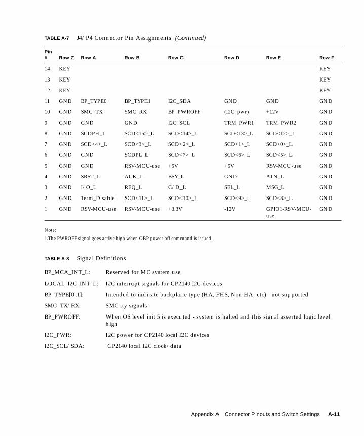
Note:
1.The PWROFF signal goes active high when OBP power off command is issued.
14 KEY KEY
13 KEY KEY
12 KEY KEY
11 GND BP_TYPE0 BP_TYPE1 I2C_SDA GND GND GND
10 GND SMC_TX SMC_RX BP_PWROFF (I2C_pwr) +12V GND
9 GND GND GND I2C_SCL TRM_PWR1 TRM_PWR2 GND
8 GND SCDPH_L SCD<15>_L SCD<14>_L SCD<13>_L SCD<12>_L GND
7 GND SCD<4>_L SCD<3>_L SCD<2>_L SCD<1>_L SCD<0>_L GND
6 GND GND SCDPL_L SCD<7>_L SCD<6>_L SCD<5>_L GND
5 GND GND RSV-MCU-use +5V +5V RSV-MCU-use GND
4 GND SRST_L ACK_L BSY_L GND ATN_L GND
3 GND I/O_L REQ_L C/D_L SEL_L MSG_L GND
2 GND Term_Disable SCD<11>_L SCD<10>_L SCD<9>_L SCD<8>_L GND
1 GND RSV-MCU-use RSV-MCU-use +3.3V -12V GPIO1-RSV-MCU-use
GND
TABLE A-8 Signal Definitions
BP_MCA_INT_L: Reserved for MC system use
LOCAL_I2C_INT_L: I2C interrupt signals for CP2140 I2C devices
BP_TYPE[0..1]: Intended to indicate backplane type (HA, FHS, Non-HA, etc) - not supported
SMC_TX/RX: SMC tty signals
BP_PWROFF: When OS level init 5 is executed - system is halted and this signal asserted logic levelhigh
I2C_PWR: I2C power for CP2140 local I2C devices
I2C_SCL/SDA: CP2140 local I2C clock/data
TABLE A-7 J4/P4 Connector Pin Assignments (Continued)
Pin# Row Z Row A Row B Row C Row D Row E Row F
Appendix A Connector Pinouts and Switch Settings A-11
TABLE A-9 MII Signals
MII_RXD<0:3>: Receive data
MII_TXD<0:3>: Transmit data
MII_RX_CLK: Receive clock
MII_TX_CLKI: Transmit clock
MII_TX_EN: Transmit enable
MII_CRS: Carrier sense
MII_COL: Collision detect
MII_RX_ER: Receive error
MII_TX_ER: Transmit error
MII_RX_DV: Receive frame detect
MII_MDIO: Transceiver management data (external)
TABLE A-10 SCSI single-ended levels - SCSI-A on J4 and SCSI-B on J5
ATN: Attention - Active low n BSY: Busy - Active low
C/D: Command or Data - Active low
I/O: Input or output data direction
MSG: Message phase indicator - active low
ACK: Acknowledge - Active low
SCD<0:15>: SCSI data lines - Active low
SCDPHSCSI : parity high byte; provides parity for SCD[8:15] - Active low
SCDPLSCSI: parity low byte; provides parity for SCD[0:7] - Active low
SEL: Select - Active low
REQ: Request - Active low
SRST: SCSI bus reset - Active low
TRM_PWR: Termination power for external SCSI terminator
A-12 Netra CP2140 Technical Reference and Installation Manual • October 2002
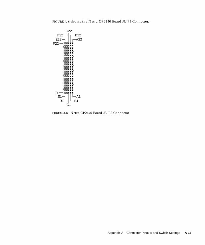
FIGURE A-6 shows the Netra CP2140 Board J5/P5 Connector.
FIGURE A-6 Netra CP2140 Board J5/P5 Connector
F22
F1
A22
C22
E22B22D22
A1E1
C1B1D1
Appendix A Connector Pinouts and Switch Settings A-13
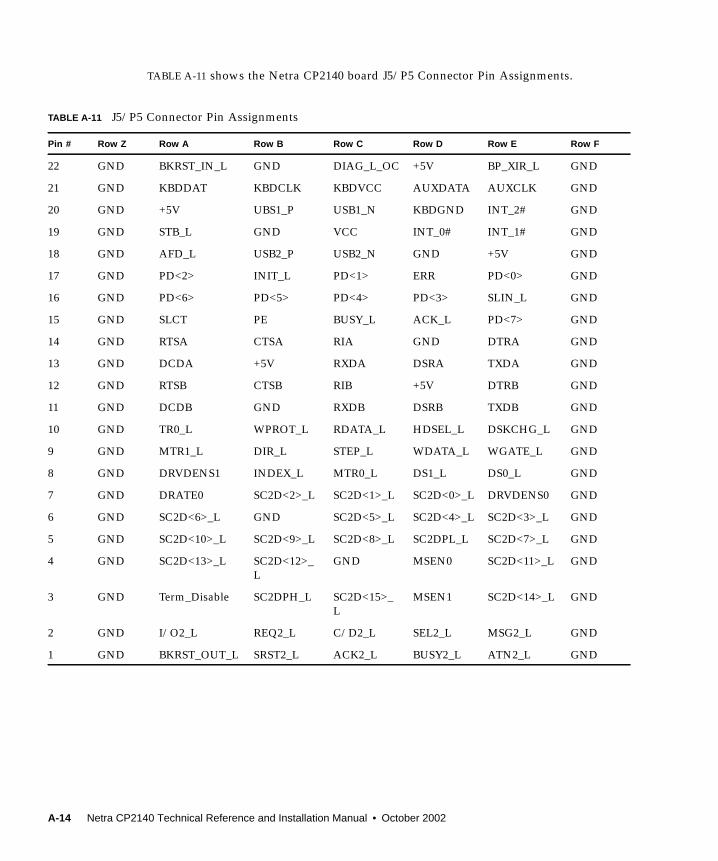
TABLE A-11 shows the Netra CP2140 board J5/P5 Connector Pin Assignments.
TABLE A-11 J5/P5 Connector Pin Assignments
Pin # Row Z Row A Row B Row C Row D Row E Row F
22 GND BKRST_IN_L GND DIAG_L_OC +5V BP_XIR_L GND
21 GND KBDDAT KBDCLK KBDVCC AUXDATA AUXCLK GND
20 GND +5V UBS1_P USB1_N KBDGND INT_2# GND
19 GND STB_L GND VCC INT_0# INT_1# GND
18 GND AFD_L USB2_P USB2_N GND +5V GND
17 GND PD<2> INIT_L PD<1> ERR PD<0> GND
16 GND PD<6> PD<5> PD<4> PD<3> SLIN_L GND
15 GND SLCT PE BUSY_L ACK_L PD<7> GND
14 GND RTSA CTSA RIA GND DTRA GND
13 GND DCDA +5V RXDA DSRA TXDA GND
12 GND RTSB CTSB RIB +5V DTRB GND
11 GND DCDB GND RXDB DSRB TXDB GND
10 GND TR0_L WPROT_L RDATA_L HDSEL_L DSKCHG_L GND
9 GND MTR1_L DIR_L STEP_L WDATA_L WGATE_L GND
8 GND DRVDENS1 INDEX_L MTR0_L DS1_L DS0_L GND
7 GND DRATE0 SC2D<2>_L SC2D<1>_L SC2D<0>_L DRVDENS0 GND
6 GND SC2D<6>_L GND SC2D<5>_L SC2D<4>_L SC2D<3>_L GND
5 GND SC2D<10>_L SC2D<9>_L SC2D<8>_L SC2DPL_L SC2D<7>_L GND
4 GND SC2D<13>_L SC2D<12>_L
GND MSEN0 SC2D<11>_L GND
3 GND Term_Disable SC2DPH_L SC2D<15>_L
MSEN1 SC2D<14>_L GND
2 GND I/O2_L REQ2_L C/D2_L SEL2_L MSG2_L GND
1 GND BKRST_OUT_L SRST2_L ACK2_L BUSY2_L ATN2_L GND
A-14 Netra CP2140 Technical Reference and Installation Manual • October 2002

TABLE A-12 Miscellaneous
BKRST_IN_L: Backplane reset input to SMC
BKRST_OUT_L: Backplane test output from SMC
BP_XIR_L: Push button reset system input. Active low
DIAG_LOC: Diagnostic / Alarm output from SMC
TABLE A-13 USB Signals
USB1_P/N: USB (Universal Serial Bus) signal pair - RIO-A
USB2_P/N: USB (Universal Serial Bus) signal pair - RIO-B
INT[0..2]: cPCI interface signal interrupts, not supported
TABLE A-14 Parallel Port
ACK_L: Pulsed by peripheral to acknowledge data sent
BUSY: Indicates a printer cannot accept more data
ERR_L: Peripheral detected an error
PD[7..0]: Parallel data lines
PE: Paper end - indicates printer is out of paper
AFD_L: auto feed - causes printer to line feed
INIT_L: initializes the peripheral
SLIN_L: select in - selects the peripheral
STB_L: data strobe - indicates data is valid
SLCT: select, peripheral indicates it is selected
TABLE A-15 Serial COM Ports (A and B), RS 232 Levels
CTS: clear to send
DCD: Data Carrier Detected
DSR: Data Set Ready
DTR: Data Terminal Ready
RI: Ring Indicator
RTS: Request to Send
RXD: Serial Receive Data
TXD: Serial Transmit Data
Appendix A Connector Pinouts and Switch Settings A-15
TABLE A-16 Floppy Disk Drive, TTL Levels
DSKCHG_L: indicates the drive door has been opened
DIR_L: controls direction of the head during step operations
DRATE[0]: reflects the value of the data transfer but in the DSR or CCR
DRVDENS[1..0]: disk density select communication in rev1.0, resvd in 1.1 n DS[1..0]: drive selects
HDSEL_L: selects top or bottom side head
INDEX_L: indicates the beginning of a track
MSEN[1..0]: used for sensing density of the media
RDATA_L: data read
STEP_L: step, pulses move head in or out
TR0_L: indicates the is positioned above track 00
WDATA_L: write data to drive
WGATE_L: enables head write circuitry of drive
WPROT_L: indicates a disk is write-protected
TABLE A-17 Keyboard/Auxiliary Device Signals
AUXCLK: Clock for PS/2 auxiliary device (mouse) - TTL levels, active high
AUXDAT: Serial data line for PS/2 auxiliary device (mouse) - TTL levels, active high
KBDCLK: Clock for PC/AT or PS/2 keyboard - TTL levels, active high
KBDDAT: Serial data line for PC/AT or PS/2 keyboard - TTL levels, active high
A-16 Netra CP2140 Technical Reference and Installation Manual • October 2002
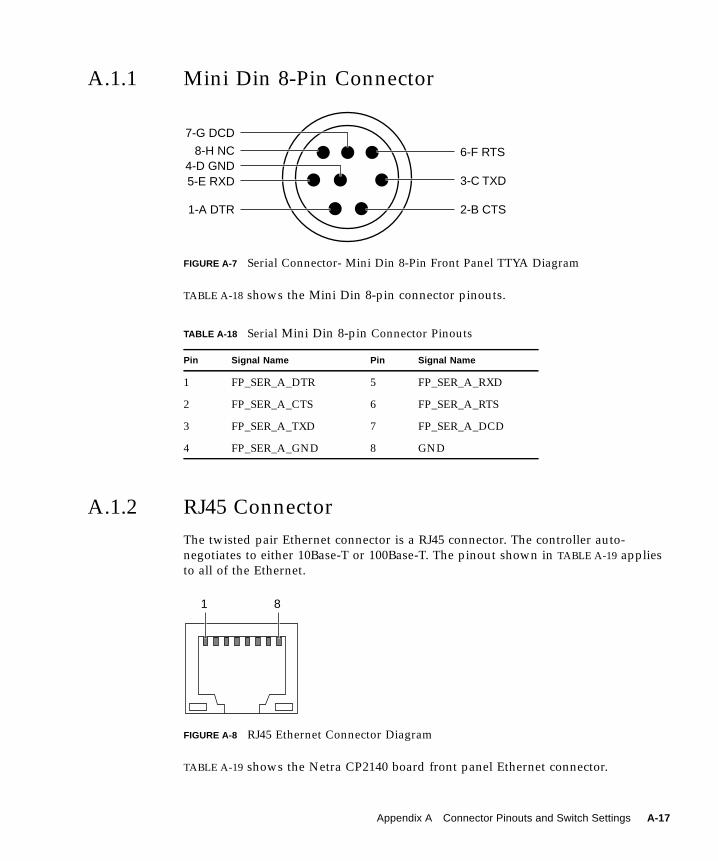
A.1.1 Mini Din 8-Pin Connector
FIGURE A-7 Serial Connector- Mini Din 8-Pin Front Panel TTYA Diagram
TABLE A-18 shows the Mini Din 8-pin connector pinouts.
A.1.2 RJ45 ConnectorThe twisted pair Ethernet connector is a RJ45 connector. The controller auto-negotiates to either 10Base-T or 100Base-T. The pinout shown in TABLE A-19 appliesto all of the Ethernet.
FIGURE A-8 RJ45 Ethernet Connector Diagram
TABLE A-19 shows the Netra CP2140 board front panel Ethernet connector.
TABLE A-18 Serial Mini Din 8-pin Connector Pinouts
Pin Signal Name Pin Signal Name
1 FP_SER_A_DTR 5 FP_SER_A_RXD
2 FP_SER_A_CTS 6 FP_SER_A_RTS
3 FP_SER_A_TXD 7 FP_SER_A_DCD
4 FP_SER_A_GND 8 GND
6-F RTS
3-C TXD
2-B CTS
8-H NC
7-G DCD
4-D GND5-E RXD
1-A DTR
1 8
Appendix A Connector Pinouts and Switch Settings A-17

A.1.3 PMC ConnectorsFIGURE A-9 shows the PMC connectors: J3001, J3002, and J3003.
TABLE A-19 Netra CP2140 Board Front Panel Ethernet Connector Pinout
Pin # Description
1 TXD+
2 TXD-
3 RXD+
4 4T_D3P
5 4T_D3P
6 RXD-
7 4T_D4P
8 4T_D4P
A-18 Netra CP2140 Technical Reference and Installation Manual • October 2002
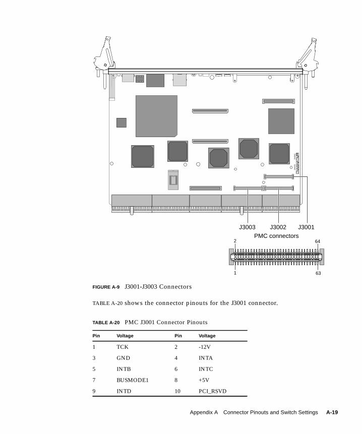
FIGURE A-9 J3001-J3003 Connectors
TABLE A-20 shows the connector pinouts for the J3001 connector.
TABLE A-20 PMC J3001 Connector Pinouts
Pin Voltage Pin Voltage
1 TCK 2 -12V
3 GND 4 INTA
5 INTB 6 INTC
7 BUSMODE1 8 +5V
9 INTD 10 PCI_RSVD
34
SV
49J
12
12
SV
28F
SW
2401
SW
1801
1
2
63
64
J3003PMC connectors
J3002 J3001
Appendix A Connector Pinouts and Switch Settings A-19

11 GND 12 PCI_RSVD
13 CLK 14 GND
15 GND 16 GNT
17 REQ 18 +5V
19 V(I/O) 20 AD31
21 AD28 22 AD27
23 AD25 24 GND
25 GND 26 CBE3
27 AD22 28 AD21
29 AD19 30 +5V
31 V (IO) 32 AD17
33 FRAME 34 GND
35 GND 36 IRDY
37 DEVSEL 38 +5V
39 GND 40 LOCK
41 SDONE 42 SBO
43 PAR 44 GND
45 V (IO) 46 AD15
47 AD12 48 AD11
49 AD9 50 +5V
51 GND 52 CBE0
53 AD6 54 AD5
55 AD4 56 GND
57 V (IO) 58 AD3
59 AD2 60 AD1
61 AD0 62 +5V
63 GND 64 REQ64
TABLE A-20 PMC J3001 Connector Pinouts
Pin Voltage Pin Voltage
A-20 Netra CP2140 Technical Reference and Installation Manual • October 2002

A.1.4 PMC J3002 Connector
TABLE A-21 PMC J3002 Connector Pinouts
Pin Voltage Pin Voltage
1 +12V 2 TRST
3 TMS 4 TD0
5 TD1 6 GND
7 GND 8 PCI_RSVD
9 PCI_RSVD 10 PCI_RSVD
11 BUSMODE2 12 +3.3V
13 RST 14 BUSMODE3
15 +3.3V 16 BUSMODE4
17 PCI_RSVD 18 GND
19 AD30 20 AD29
21 GND 22 AD26
23 AD24 24 3.3V
25 IDSEL 26 AD23
27 +3.3V 28 AD20
29 AD18 30 GND
31 AD16 32 CBE2
33 GND 34 PMC_RSVD
35 TRDY 36 +3.3V
37 GND 38 STOP
39 PERR 40 GND
41 +3.3V 42 SERR
43 CBE1 44 GND
45 AD14 46 AD13
47 GND 48 AD10
49 AD8 50 +3.3V
51 AD7 52 PMC_RSVD
53 +3.3V 54 PMC_RSVD
55 PMC_RSVD 56 GND
Appendix A Connector Pinouts and Switch Settings A-21

A.1.5 PMC J3003 Connector
57 PMC_RSVD 58 PMC_RSVD
59 GND 60 PMC_RSVD
61 ACK64 62 +3.3V
63 GND 64 PMC_RSVD
TABLE A-22 PMC J3003 Connector Pinouts
Pin Voltage Pin Voltage
1 IO1 2 IO2
3 IO3 4 IO4
5 IO5 6 IO6
7 IO7 8 IO8
9 IO9 10 IO10
11 IO11 12 IO12
13 IO13 14 IO14
15 IO15 16 IO16
17 IO17 18 IO18
19 IO19 20 IO20
21 IO21 22 IO22
23 IO23 24 IO24
25 IO25 26 IO26
27 IO27 28 IO28
29 IO29 30 IO30
31 IO31 32 IO32
33 IO33 34 IO34
35 IO35 36 IO36
37 IO37 38 IO38
39 IO39 40 IO40
41 IO41 42 IO42
TABLE A-21 PMC J3002 Connector Pinouts
Pin Voltage Pin Voltage
A-22 Netra CP2140 Technical Reference and Installation Manual • October 2002
FIGURE A-10 shows the location of memory module connectors J0601 and J0602,respectively.
43 IO43 44 IO44
45 IO45 46 IO46
47 IO47 48 IO48
49 IO49 50 IO50
51 IO51 52 IO52
53 IO53 54 IO54
55 IO55 56 IO56
57 IO57 58 IO58
59 IO59 60 IO60
61 IO61 62 IO62
63 IO63 64 IO64
TABLE A-22 PMC J3003 Connector Pinouts
Pin Voltage Pin Voltage
Appendix A Connector Pinouts and Switch Settings A-23

FIGURE A-10 Memory Module Connectors J0601 and J0602
34
SV
49J
12
12
SV
28F
SW
2401
SW
1801
1002
991
SDRAM memorymodule connectors
J0601
J0602
A-24 Netra CP2140 Technical Reference and Installation Manual • October 2002

A.2 Memory Module Connector PinoutTABLE A-23 and TABLE A-24 show the memory module connector 1 and 2 pinouts.
TABLE A-23 Memory Module Connector 1 Pinout (Bottom Side)
Pin # Front Side Pin # Front Side Pin # Back Side Pin # Back Side
99 VDD_3.3V 49 AB3 100 VSS 50 DQ9
97 DQ43 47 AA2 98 DQ0 48 DQ10
95 DQ42 45 VSS 96 DQ1 46 VDD_3.3V
93 DQ41 43 AB2 94 DQ2 44 DQ11
91 VSS 41 AA1 92 VDD_3.3V 42 DQ12
89 DQ40 39 AB1 90 DQ3 40 DQ13
87 DQ35 37 VDD_3.3V 88 DQ4 38 VSS
85 VDD_3.3V 35 AA0 86 VSS 36 DQ14
83 DQ34 33 AB0 84 DQ5 34 DQ15
81 DQ33 31 VSS 82 DQ6 32 VDD_3.3V
79 DQ32 29 CK3 80 DQ7 30 CK1
77 VSS 27 VDD_3.3V 78 VDD_3.3V 28 VSS
75 CK2 25 S1 76 CK0 26 S0
73 VSS 23 S5 74 RAS0 24 S4
71 NC 21 DQ27 72 RAS2 22 DQ16
69 VDD_3.3V 19 DQ26 70 VSS 20 DQ17
67 AA6 17 VSS 68 CAS0 18 VDD_3.3V
65 AB6 15 DQ25 66 CAS2 16 DQ18
63 AA5 13 DQ24 64 WE0 14 DQ19
61 VSS 11 ALERT 62 VDD_3.3V 12 DQ20
59 AB5 9 VDD_3.3V 60 WE2 10 VSS
57 AA4 7 SA2 58 CKE0 8 DQ21
55 AB4 5 SA1 56 CKE2 6 DQ22
53 VDD_3.3V 3 NC 54 VSS 4 DQ23
51 AA3 1 VDD_3.3VI2C 52 DQ8 2 VDD_3.3V
Appendix A Connector Pinouts and Switch Settings A-25

TABLE A-24 Memory Module Connector 2 Pinout (Bottom Side)
Pin # Front Side Pin # Front Side Pin # Back Side Pin # Back Side
99 VSS 49 DQ62 100 VDD_3.3V 50 AB10
97 DQ71 47 DQ61 98 DQ47 48 AA9
95 DQ70 45 VDD_3.3V 96 DQ46 46 VSS
93 DQ69 43 DQ60 94 DQ45 44 AB9
91 VDD_3.3V 41 DQ59 92 VSS 42 AA8
89 DQ68 39 DQ58 90 DQ44 40 AB8
87 DQ67 37 VSS 88 DQ39 38 VDD_3.3V
85 VSS 35 DQ57 86 VDD_3.3V 36 AA7
83 DQ66 33 DQ56 84 DQ38 34 AB7
81 DQ65 31 VDD_3.3V 82 DQ37 32 VSS
79 DQ64 29 CK4 80 DQ36 30 CK6
77 VDD_3.3V 27 VSS 78 VSS 28 VDD_3.3V
75 CK5 25 S3 76 CK7 26 S2
73 RAS1 23 S7 74 BAA1 24 S6
71 RAS3 21 DQ55 72 BAB1 22 DQ31
69 VSS 19 DQ54 70 VDD_3.3V 20 DQ30
67 CAS1 17 VDD_3.3V 68 BAA0 18 VSS
65 CAS3 15 DQ53 66 BAB0 16 DQ29
63 WE1 13 DQ52 64 AA12 14 DQ28
61 VDD_3.3V 11 DQ51 62 VSS 12 LCLK-I
59 WE3 9 VDD_3.3V 60 AB12 10 VSS
57 CKE1 7 DQ50 58 AA11 8 LCLK-O
55 CKE3 5 DQ49 56 AB11 6 SDA
53 VSS 3 DQ48 54 VDD_3.3V 4 SCK
51 DQ63 1 VDD_3.3V 52 AA10 2 VSS
A-26 Netra CP2140 Technical Reference and Installation Manual • October 2002

A.3 SMC Switch Settings for HA and Non-HA SystemsThe switches on the CP2140 SMC Module serve two purposes:
■ Establish backplane type (HA or non-HA)
■ Select Boot Device (Boot Flash or SMC config block setting)
SW0501.Switch1 is for HA/Non-HA settings and SW0501.Switch2 is for flash deviceselection based on SMC settings.
A.3.1 Setting Non-HA SystemsIf you have a non-HA system, set the SMC module switch settings before poweringon the Netra CP2140 board unit.
■ SW0501.Switch1 ---> Closed (switch is set in the direction of the arrow)
■ SW0501.Switch2 ---> Closed (switch is set in direction of arrow)
See FIGURE A-11 for the location of SW0501 on the Netra CP2140 board.
FIGURE A-11 Setting Switches to Closed Position
SMC module
34
SV
49J
12
12
SV
28F
SW
2401S
W1801
12
SV
28F
12
SV
28F
SW0501
Appendix A Connector Pinouts and Switch Settings A-27

FIGURE A-12 SW0501 Position for non-HA Systems
A.3.2 Setting HA SystemsIf the user has a HA system, set the SMC switch settings before powering on theCP2140 unit as follows:
■ SW0501.Switch1 ---> Open (switch is set opposite to arrow direction)
■ SW0501.Switch2 ---> Closed (switch is set in direction of arrow)
See FIGURE A-13 for location of SW0501.
FIGURE A-13 Location of SW0501 on SMC Module
FIGURE A-14 shows how to set switch positions for HA systems.
1 2
SMC module
34
SV
49J
12
12
SV
28F
SW
2401S
W1801
12
SV
28F
12
SV
28F
SW0501
A-28 Netra CP2140 Technical Reference and Installation Manual • October 2002

SV49J
FIGURE A-14 SW0501 Switch Setting for HA Systems
A.4 SCSI and Flash Switch SettingsTwo sets of switches on the Netra CP2140 board perform two different functions:
■ SW1801 for flash device selection■ SW2401 for SCSI termination
The positions of these switches determine the flash device selection and SCSItermination. If a switch is moved in the direction of the arrow, it is closed (ON). If aswitch is moved in the opposite direction of the arrow, it is open (OFF). FIGURE A-15shows switches and the switch setting legend.
Note – The default for both the SW2401 and SW1801 switches is Open/Off.
FIGURE A-15 Switch Setting Legend
A.4.1 Flash Device Selection SwitchesThe position of the two SW1801 switches determines the flash device selection onthe board. TABLE A-26 describes the flash device selection.
1 2
1 2
Open/Off Closed/On
SW1801 flash device selection switches SW2401 SCSI device selection switches
SV28F
1 2
Open/Off Closed/On
3
Open/Off
4
Open/Off
Appendix A Connector Pinouts and Switch Settings A-29

A.4.2 SCSI Termination SwitchesFour SW2401 SCSI termination switches are located on the board.
The SCSI switches operate independently from each other and can be set to Open orClosed position. FIGURE A-16 shows an example of SCSI termination switch settings.
FIGURE A-16 SCSI Termination Switch Setting Example
TABLE A-26 describes the SCSI termination switch setting.
TABLE A-25 Flash Device Switch Setting (SW1801)
PositionSwitch No. 1
PositionSwitch No. 2 Description
Open Open
OBP 1 MB boot flashselected (default)Should never be useradjusted
Closed Closed
User flash 1 selected
Open Closed
User flash 1 and 2 selected
1 2
1 2
1 2
SW2401 SCSI device selection switches
1 2
Open/Off Closed/On
3
Open/Off
SV49J
4
Open/Off
A-30 Netra CP2140 Technical Reference and Installation Manual • October 2002

See FIGURE A-17 for the location of flash device, SCSI, and SMC FPGA (SW0501)switches.
TABLE A-26 SCSI Termination Switch Setting (SW2401)
Position Switch 1 Switch 2 Switch 3 Switch 4
Open Terminationpower suppliedfor SCSI Bus A.
Terminationpower suppliedfor SCSI Bus B.
Terminationenabled for SCSIBus A.
Terminationenabled for SCSIBus B.
Closed Terminationpower notsupplied for SCSIBus A.
Terminationpower notsupplied for SCSIBus B.
Terminationdisabled for SCSIBus A.
Terminationdisabled for SCSIBus B.
Appendix A Connector Pinouts and Switch Settings A-31

FIGURE A-17 SCSI Switch Selections and SMC on the Netra CP2140 Board
34
SV
49J
12
12
SV
28F
SW
2401S
W1801
34
SV
49J
12
12
SV
28F
SW
2401S
W1801
12
SV
28F
12
SV
28F
A-32 Netra CP2140 Technical Reference and Installation Manual • October 2002
APPENDIX B
Mechanical Drawings
This appendix provides mechanical drawings for the CP2140.
FIGURE B-1 shows the mechanical drawing of the front panel.
FIGURE B-2 shows the mechanical dimensions of the CP2140.
FIGURE B-3 and FIGURE B-4 show the mechanical dimensions of the CP2140 board withheatsink and memory modules.
B-1

FIGURE B-1 Mechanical Drawing of the Netra CP2140 Board Front Panel
ABORT
P
M
C
RESET
COM
CP2140-650
HOTSWAP
ALARM/USER
READY
microsystems
72.10
255.85
222.25
R3.254x
R3.254x
R1.905x
235.40232.20
223.85
151.75144.10
133.60
111.34
94.80
78.10
24.10
12.80
0.00
0.00
3.70
6.90
10.2
019
.80
R6.30
PANEL SILK SCREEN
PANEL EMI SHIELD
118.09
ETHERNET
2.50
16.0
0
6.10
6.90
B-2 Netra CP2140 Technical Reference and Installation Manual • October 2002

FIGURE B-2 Mechanical Dimensions of the Netra CP2140 Board
19.80
43.9037.90
233.35
49.90
160.00
PMC
AB
OR
T
RE
SE
T
CO
M
CP
2140-850
HO
TS
WA
P
ALA
RM
/U
SE
R
RE
AD
Y
micro
system
s
ETH
ER
NE
T
Appendix B Mechanical Drawings B-3

FIGURE B-3 Netra CP2140 Board Mechanical Dimensions of the Heat sink and Single-wide Memory Module
93 mm 47.50 mm
PMC
AB
OR
T
RE
SE
T
CO
M
CP
2140-850
HO
TS
WA
P
ALA
RM
/U
SE
R
RE
AD
Y
micro
system
s
ETH
ER
NE
T
B-4 Netra CP2140 Technical Reference and Installation Manual • October 2002
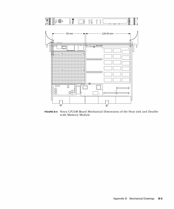
FIGURE B-4 Netra CP2140 Board Mechanical Dimensions of the Heat sink and Double-wide Memory Module
93 mm 126.50 mm
PMC
AB
OR
T
RE
SE
T
CO
M
CP
2140-850
HO
TS
WA
P
ALA
RM
/U
SE
R
RE
AD
Y
micro
system
s
ETH
ER
NE
T
Appendix B Mechanical Drawings B-5

B-6 Netra CP2140 Technical Reference and Installation Manual • October 2002

APPENDIX C
SunVTS
This appendix describes the SunValidation Test Suite (SunVTS ) , a comprehensivesoftware package that tests and validates the Netra CP2140 board by verifying theconfiguration and function of most hardware controllers and devices on themotherboard. SunVTS software is used to validate a system during development,production, inspection, troubleshooting, periodic maintenance and system orsubsystem stressing. SunVTS software can be tailored to run on various types ofsystems, ranging from desktops to servers with modifiable test instances andprocessor affinity features.
You can perform high-level system testing using the appropriate version of SunVTS.For detailed information on SunVTS support, visit the following web sites:
http://www.sun.com/oem/products/vts/index.html
The following provides some information on distribution of SunVTS software:
■ SunVTS software can be downloaded from the following URL:
http://www.sun.com/oem/products/vts/index.html
■ Ensure that the SunVTS software version is compatible with the Solaris operatingenvironment version being used.
Solaris 8 2/02 operating environment is compatible with SunVTS 4.6 package.
■ Information on the version of the SunVTS software installed can be found in thefile:
/opt/SUNWvts/bin/.version
■ The SunVTS packages are also located on the Solaris 8 Supplemental Software CDfor Sun Computer Systems that ships with the Solaris operating environmentrelease.
■ To obtain SunVTS documentation, contact your local customer servicerepresentative or Field Application Engineer.
C-1

C-2 Netra CP2140 Technical Reference and Installation Manual • October 2002
APPENDIX D
Solaris Sun FRU ID
The Solaris Sun FRU ID information is stored on the Netra CP2140 board EEPROM(U3209) and is used to identify the board for service purposes. The Solaris Sun FRUID is one of the standard features in the Solaris 8 2/02 operating environment andlater compatible versions. The CP2000 Supplemental 4.0 CD for Solaris 8 implementsSolaris Sun FRU ID for the CP2140 board, when used with Solaris 8 update 2/02 andlater compatible versions.
To access the Solaris Sun FRU ID infomation for the CP2140 board, use the prtfrucommand. See the prtfru(1M) man pages for futher infomation on this command.The man pages can be found on the Solaris 8 2/02 operating environment defaultpackage.
D.1 Prtfru CommandBy typing in the prtfru command at the Solaris command line, the user can obtainan output with Solaris Sun FRU ID information that is similar to the example shownbelow. The fields that are displayed in the example are described below in TABLE D-1.
D-3

# prtfru
/frutree
/frutree/chassis (fru)
/frutree/chassis/CPU-slot?Label=CPU
/frutree/chassis/CPU-slot?Label=CPU/CPU-slot (container)
SEGMENT: SD
/ManR
/ManR/UNIX_Timestamp32: Fri May 11 19:00:00 PDT 2001
/ManR/Fru_Description:
/ManR/Manufacture_Loc:
/ManR/Sun_Part_No: 375-302
/ManR/Sun_Serial_No: 001379
/ManR/Vendor_Name: Sun Microsystems
/ManR/Initial_HW_Dash_Level:
/ManR/Initial_HW_Rev_Level:
/ManR/Fru_Shortname: CP2140
/frutree/chassis/CPU-slot?Label=CPU/CPU-slot/c0?Label=c0
#
TABLE D-1 Description of Fields in Typical Prtfru Command Display Output
Field Description
/ManR/UNIX_Timestamp32: Fri May 1119:00:00 PDT 2001
Board manufacturing timestamp
/ManR/Fru_Description: Description for the board field replaceable unit
/ManR/Manufacture_Loc: Location where board is manufactured
/ManR/Sun_Part_No: 375-302 Board identification part number
/ManR/Sun_Serial_No: 001379 Board identification serial number
/ManR/Vendor_Name: Sun Microsystems Name of the board vendor
D-4 Netra CP2140 Technical Reference and Installation Manual • October 2002

/ManR/Initial_HW_Dash_Level: Board identification dash number
/ManR/Initial_HW_Rev_Level: Board identification revision number
/ManR/Fru_Shortname: CP2140 Short name for the board such as CP2140
TABLE D-1 Description of Fields in Typical Prtfru Command Display Output
Field Description
Appendix D Solaris Sun FRU ID D-5

D-6 Netra CP2140 Technical Reference and Installation Manual • October 2002

Glossary
AP Alternate Pathing (AP) is a software-driven facility that employs bothredundant hardware and redundant software driver paths between a serverand a disk array or a network. If one path fails, AP ensures that the disk arrayor network is still available through the alternate path. For example, thealternate path can be a second port on an interface board, or an entirelyseparate interface board. See also Device Reconfiguration.
ASM Advanced System Monitoring
Availability The ratio of the total time that a functional unit is capable of being used to thetotal time that the unit is required for use.
BMC Baseboard Management Controller: The BMC is used to manage chassisenvironmental, configuration and service functions, and receive event datafrom other parts of the system. It receives data through sensor interfaces andinterprets these data by using the Sensor Data Repository (SDR) to which itprovides an interface. The BMC provides another interface to the System EventLog (SEL). The BMC allows Both the SDR and the SEL to be accessed from thesystem or from the Intelligent Platform Management Bus (IPMB). A typicalfunction of the BMC is to measure processor temperature, power supplyvalues, and cooling fan status. It can take some autonomous actions to preservesystem integrity. For example, it might switch on a fan at a particulartemperature threshold. An application interface may be provided to enablecustom user-management applications to be built.The BMC describes an abstract function, or role. It carries no definition of howit might be implemented.
Boot: The process of initializing the hardware to execute and run an operatingenvironment such as Solaris 2.6 5/98 or subsequent compatible versions.
Checkpoint (1) A point at which information about the status of a job and the system canbe recorded so that the job can later be restarted from that point. (2) Asequence of instructions in a computer program for recording the status ofexecution for restarting. v. to checkpoint; n. checkpointing.
Glossary-7
CompactPCI An adaptation of the PCI bus architecture defined in the PeripheralComponent Interconnect (PCI) Specification 2.1 (or later) to an electrically-compatible robust industrial form. This form specifies a Eurocard-style printedcircuit board assembly (PCBA) that uses “hard metric” connectors to connect itto the enclosure backplane. CompactPCI is an open specification supported bythe PCI Industrial Computers Manufacturers’ Group (PICMG).
CompactPCI Bridge The PCI bridge between the System Host processor and the CompactPCI bus.The CompactPCI bridge must reside in the system slot to provide CompactPCIclocking and arbitration that are only available from that slot. CompactPCIbridges maybe controllable by the System Management Controller to turn offclocks and arbitration.
DeviceReconfiguration A process that is used in the Netra CP2140 board system to configure (add) or
deconfigure (remove) device tree allocations and load or unload softwaredriver modules while the system is running. It is analogous to DynamicReconfiguration that is used on some Sun high-end server systems with someimportant differences. It is not used to reconfigure memory or CPU resourcesand it can be used automatically in the Full Hot-Swap and HA Hot-Swap caseswhen the Hot-Swap framework software is prompted by the SystemManagement Controller (when HA is available). Netra CP2140 board HAdevice reconfiguration can also be invoked manually from a console.
Device Tree The OpenBoot PROM probing process constructs a hierarchical representationof the hardware devices that are found on the bus, the host-bus being the root.The device tree includes several device nodes. (Ethernet is a device node.)
Dropin A code or data module which can be called by the OpenBoot PROM duringsystem startup. It is placed in unused memory space between OpenBootPROM and POST. User-created dropins are usually used to initialize customuser hardware. They do not require that the user possesses OpenBoot PROMsource code; only the binary OpenBoot PROM image need be licensed. Dropinsare used to add firmware drivers for user hardware.
DynamicReconfiguration Dynamic Reconfiguration (DR) is a software package that enables the
administrator to (1) view a system configuration; (2) suspend or restartoperations involving a port, storage device, or board; and (3) reconfigure thesystem (detach or attach hot-swappable devices such as disk drives or interfaceboards) without the need to power down the system. When DR is used withAlternate Pathing or Solstice DiskSuite™ software (and redundant hardware),the server can continue to communicate with disk drives and networkswithout interruption while a service provider replaces an existing device orinstalls a new device. DR supports replacement of a CPU/Memory, providedthe memory on the board is not interleaved with memory on other boards inthe system. Note that DR is used with Sun high-end server systems. See DeviceConfiguration for the analogous process that is applied to the Netra CP2140board.
Glossary-8 Netra CP2140 Technical Reference and Installation Manual • October 2002

Failover The process of transfer of function from a failed component subsystem to analternate one while preserving the operational state of the overall system. Thefunctions transferred may include those of control and management.
Firmware An ordered set of instructions and data that is stored in a way that isfunctionally independent of main storage, for example, microprograms storedin a read-only memory (ROM). The term firmware describes microcode in ROM.At the time they are coded, microinstructions are software. When they are putinto ROM, they become part of the hardware (microcode) or a combination ofhardware and software (microprograms). Usually, microcode is permanent andcannot be modified by the user but there are exceptions.
FRU Field Replaceable Unit: A part or subsystem that can be replaced in the field orat a customer site. Parts that are not FRUs are only factory replaceable.
HA High-availability: the property of a system associated with a high in-service toout-of service time ratio. This property can be engineered by reconfiguring thesystem “on the fly” to isolate failed elements so they can be replaced withoutaffecting the operational condition.
Hardware On the CP2140, CPU, cables, and peripheral devices are typical examples ofhardware.
heartbeat A repetitive signal passed from one system to another to communicate thestate of integrity or “health” of the sending system.
Host Computer Host Computer (context-dependent): (1) A computer that usually performsnetwork control functions and provides end-users with services such ascomputation and database access.(2) The primary or controlling computer in a multi-computer installation.
Hot Swap Insertion into a running system (3 modes: basic, full and HA).
Hot-swap Controller The controller that takes care of the low-level sequencing associated with hotswap.
HS Hot-swap: The capability or property of a system element to be removed orreplaced while the system hardware is nominally operating under power. Thiscapability is usually invoked after a failure and is implemented by a sequencethat steers the functions of the element to other parts of the system.
Hot-swap, as defined by PICMG, can be classified as Basic, Full, or HA.
Basic HS requires manual software sequencing to bring a card out ofcommission.
Full HS uses hardware enumeration signals to indicate board status. Softwareautomatically decommissions the card. (HA hot swap is not supported in theCP2140 configuration.)
Glossary-9

I2C Inter-Integrated Circuit Bus: a serial bus developed by Philips for inter-package communications and typically used by them in TV sets. In SunCompact PCI systems, it is used to link card elements in a system formanagement communications.
ICMB Inter-chassis Management Bus: an IPMI/I2C bus (analogous to the IPMB) usedto accomplish chassis-to-chassis management.
IPMB Intelligent platform management bus: a bus that carries serial communicationsignals that comply with the IPMI; it is used to communicate between CompactPCI PCBAs in a chassis.
IPMI Intelligent Platform Management Interface: IPMI is a protocol interface with aprotocol stack that includes link, transport and session layers to providereliability. It resides on an I2C physical layer.
KCS interface Keyboard Control Style interface: This interface is defined in the IPMISpecification. It is one of the BMC to System Management Software (SMS)interfaces.
Nines Used as a measure of system availability: three nines > 99.9%, four nines >99.99%, five nines > 99.999%, and six nines > 99.9999%.
Node An addressable point on a network. Each node in a Sun network has a differentname. A node can connect a computing system, a terminal, or various otherperipheral devices to the network.
Non-host / Satellite Peripheral slots / boards in the Compact PCI backplane.
NVRAMRC Non-Volatile Random-Access Memory Run Command. This refers to theexecutable OpenBoot PROM script that is written in the NVRAM. Other textinformation or binary data may exist in the NVRAM, but is not referred asNVRAMRC.
OpenBoot PROM This refers to a firmware program that consists of executable code by the CPU.This code initializes the hardware, performs Power On Self-Test (POST) andboots the system to bring up the Solaris Operating Environment. TheOpenBoot PROM, or system PROM, contains code to run POST and a suite ofuser-accessible subsystem hardware tests. It has a Forth interpreter for customuser routines. Under a normal boot sequence, it provides a path to a systemboot device which is accessed after POST completes. “Open Firmware” iscontrolled by IEEE Standard 1275.
Partition The functional entity that includes a host—with a host PCI bridge—and theperipherals that it controls on the CompactPCI bus. The partition managementis performed by the CompactPCI bus bridge on a compliant board. A partitionis analogous to a PCI domain with the difference that partition integrity is notguaranteed for boards that do not contain 21554 bridges.
PCI domain The functional entity that includes a host—usually with a host PCIbridge—and the peripherals that it controls. The domain does not necessarilyuniquely include the PCI bus because this bus can be shared by multiple
Glossary-10 Netra CP2140 Technical Reference and Installation Manual • October 2002

domains. For example, a second domain can comprise a second host/bridgeelement that controls a different set of peripherals on a shared bus. Separationand management of the domains is implemented by a controlling systemmechanism that guarantees their mutual protection.
Peripheral host Also Satellite host: performs computing-intensive functions in response tocommands from the system host. A peripheral host is limited to on-board I/O.
PICMG PCI Industrial Computers Manufacturers’ Group
PM Peripheral Management Controller
PMC PCI Mezzanine Card
POST Power-on Self Test: a suite of tests run out of system firmware before any othercode is loaded. The purpose of such testing is to check the integrity of thehardware before loading a software system.
Probing A process implemented in the firmware and software to identify onboardhardware devices and add-on cards on the CPCI back plane. The probingprocess creates the device-tree.
RARP Reverse Address Resolution Protocol; The protocol broadcasts a MAC(Ethernet) address and receives an IP address in response from a RARP server.
RAS Reliability, Availability and Serviceability: the general concepts associated withhigh in-service time systems and their simplicity of maintenance.
RCM Reconfiguration Coordination Manager
Reliability The ability of a functional unit to perform a required function under statedconditions for a stated period of time.
Satellite host See Peripheral host.
SDR Sensor Data Repository: the database that the BMC uses to determine whatsensors, FRU devices, and management controllers are in the system. Thisdatabase contains an account of sensor locations, properties, and associations.
Segment The extent to which a backplane and cards combination can be extended byaccounting for signal loading. In Compact PCI, a segment spans a maximum ofeight card slots, beyond which some bridge elements (system bridge) areneeded to provide expansion into another segment.
SEL System Event Log: the database of measured values and events that is createdby the BMC based upon its sensor monitoring. This database resides in thehost and is accessible by high-level applications.
Serviceability The capability of performing effective problem determination, diagnosis, andrepair on a data-processing system.
Glossary-11

SMC System Management Controller: There is a System Management Controller oneach card in the enclosure. One of these cards either assumes control bycommand or takes control after negotiation with the other System ManagementControllers. The System Management Controller manages peripherals toimprove the availability of the system. Through the IPMB, this entity receivesinformation on IDs of, or problems with, cards in the system and cancommunicate that information with other cards or with a system host viaanother bus. The SC can switch the PCI bridge, PCI arbitration, and PCIclocking on or off.
Software A collection of machine readable information, instructions, data, andprocedures that enable the computer to perform specific functions. Typicallystored on removable media.
System Controller Host CPU board in the System Slot of the CompactPCI backplane
System Host A system host accepts interrupts and owns peripherals. It executes userapplications and decides the distribution of tasks and within a system. In hot-swap systems the system host acts as a traffic router and functions to activateand deactivate peripheral cards (plug-in boards). It is not a Compact PCIrequirement that the system host reside in a system slot although this isnormally the case. If it resides in a peripheral slot that slot must be wired toreceive peripheral interrupts from the backplane.
System ManagementBus A serial bus that carries data and control signal between System Management
Controllers on peripheral boards and devices. Communications on this bus usethe IPMI protocol over an I2C hardware layer.
System Slot The card location in an enclosure that provides for Compact PCI clocking andarbitration. It follows that the Compact PCI bridge, which supplies thesefunctions, must be in the system slot.
System-slot Bridge Provides clocks and arbitration. This device must be controllable fromsomewhere. It can be controlled from a controller. The system host need notreside on the same card but the card that performs the function of system hostmust be able to talk to the slot containing the system-slot bridge.
System-slotController The System-slot Controller is the board that contains both the System Host and
the System Management Controller.
TFTP Trivial File Transfer Protocol; a reduced form of File Transfer Protocol (FTP).
Glossary-12 Netra CP2140 Technical Reference and Installation Manual • October 2002
Index
AABORT, 1–8addresses
Ethernet, 2–30, 2–31Advanced PCI Bridge (APB), 4–4, 5–5ALARM/USER, 1–8ambient conditions, 3–2Arbiter, 5–18arbiter, 5–18ASM Support, 6–16
Bbackplane, 2–29Backplane and Cardcage Considerations, 2–29Baseboard Management Controller, 5–10Baseboard Management Controller (BMC), 5–7Basic hot swap, 1–7blue LED, 2–23board features and specifications
CPU, 3–2Board Identification, 1–11
Ccardcage, 2–29Carrier-grade, 1–5cfgadm, 2–24chassis, 2–18check list
system, 2–7clock, 5–4
COM, 1–8command interface
host-SMC, 5–11Compact PCI
CompactPCI Connectors, A–1CompactPCI
Backplane, A–3connectors
Ethernet, A–17PMC, A–18
PMC J3002 Connector, A–21PMC J3003 Connector, A–22
RJ45 Connector, A–17Serial Connector- Mini Din 8 -Pin, A–17
COREexecution control, 6–9firmware CORE features, 6–15
CORE and BPOSTfirmware, 6–2
CORE execution controlfirmware, 6–9
CORE NVRAMfirmware variables, 6–9
Countdown register timer, 5–11CPOST and EPOST
firmware, 6–4CPU
features and specifications, 3–2
DDC/DC converter, 5–16determine local network IP addresses and
Index-13
hostnames, 2–9device node, Ethernet, 1–8DIN 8, 1–6documents, 2–8double-sized, 1–5Dual SCSI, 5–8
EEEPROM, 5–3ejector handle, 2–23environmental conditions, 3–5ESD, 2–10Ethernet, 1–8, 2–22, 4–1, 5–8
address, 2–30, 2–31connectors, A–17device node, 1–8RJ45, A–17
Ethernet support, 1–6event receiver
host-to-host communication, 6–33
FField Application Engineer, 2–7firmware
CORE and BPOST, 6–2CORE execution control, 6–9CORE Features, 6–15CPOST and EPOST, 6–4determining firmware version, 6–18determining identification numbers, 1–12field CORE/OBP firmware upgrade, 6–21firmware diagnostics, 6–38
Basic POST (BPOST), 6–39comprehensive POST (CPOST), 6–40extended POST, 6–40OpenBoot Diagnostics (OBDiag), 6–42OpenBoot PROM On-Board diagnostics, 6–42setting diagnostic levels, 6–39
initialization firmware, 6–1memory map, 6–13OBP, 6–4
Firmware NVRAM Variables, 6–9firmware variables
CORE NVRAM, 6–9firmware version, determining, 6–18
FRU ID, 1–3Full hot swap, 1–8
Ggenerating event from SPARC
host-to-host communication, 6–34ground strap, 2–10
HHA hot swap, 1–8Hardware Configurations, 2–2hardware description
physical, 4–1summary, 4–3
heartbeat, monitoring, 5–11Host-to-Host Communication, 6–31host-to-host communication
event receiver, 6–33generating event from SPARC to send to another
SPARC, 6–34packet, 6–32protocol, 6–33
HOT SWAP, 1–8hot swap, 1–6, 5–17
basicline card, 2–24
fullline card, 2–25
support, 1–7hot-swap operation, 1–5
II/O connectors, 1–8I2C EEPROM, 2–16Initial Power-On and Firmware Update, 2–29installation procedure, 2–10Interrupts, 5–11IP address, 2–9IPMI, 5–10IPMI Packet, 6–24
Index-14 Netra CP2140 Technical Reference and Installation Manual • October 2002

LLED, 5–8limits, ambient, 3–2lithium battery, 3–7local area network (LAN), 2–9
Mmain memory
features and specifications, 3–3materials and tools required, 2–11mechanical
features and specifications, 3–5media-independent interface, 4–5memory map
firmware, 6–13memory module
connector pinout, A–25installation, 2–12
MII, 5–8mini-DB9, 1–6MOSFET switches, 5–17MTBF, 3–6
NNEBS, 1–7Netra 2140 board
determining identification numbersfirmware, 1–12software, 1–12
features and specifications, 3–1Netra CP2140 board
configuring hardware, 2–12determining identification numbers, 1–10
assembly identification, 1–10environmental conditions, 3–5features and specifications
main memory, 3–3mechanical, 3–5PCI mezzanine module interface, 3–4
memory module installation, 2–12PMC module installation, 2–14software requirements, 1–9system configuration, 1–4
Netra CP2140 cardinstalling, 2–18
Netra CP2140 computeradd cPCI cards and drivers, 2–28set up, 2–22
networkset up, 2–31
NFS, 2–9non-transparent PCI bridge (NTB), 4–4NVRAM, 5–3, 5–16
OOBP
firmware, 6–4firmware upgrading, 6–21, 6–22getting latest version, 2–8OBP configuration variables, 6–10OBP Flash Update, 6–19
OBP configuration variablesOBP, 6–10
OBP flash updateAccessing SMC Config Block, 6–19Sequence to Boot Up the Correct OBP Image, 6–
22Using Flash Update Commands, 6–20
Orderable Items, 2–3
Ppacket
host-to-host communication, 6–32PCI, 2–29PCI Interface Module (PIM), 5–8PCI Mezzanine Card, 2–15PCI Mezzanine Card (PMC), 2–14, 5–8PCI Mezzanine Connectors, 1–5PCI mezzanine module interface
estimated power requirements, 3–4features and specifications, 3–4
PCI-to-PCI bridge, 5–6PICMG, 1–1PIM card, 1–6PLD, 5–18PMC module
installation, 2–14PMC Support, 1–7power budgeting, 2–8Power Module, 5–16
Index-15

power subsystem, 5–15Pre-timeout timer, 5–11Programmable Logic Device (PLD), 5–18PROM contents, 6–13protocol
host-to-host communication, 6–33
RREADY, 1–8Reliability, 3–6RESET, 1–8Reset, 5–11RIO A, 4–5RIO B, 4–4, 4–5RJ45 Ethernet, A–17
Ssatellite board, 1–1SCSI, 2–23, 2–27, 5–7SCSI termination switches, A–30serial EEPROM
replacing, 2–16SMC
SMC Implementation Note, 6–35switch settings
HA, A–28Non_HA, A–27
SMC Firmware Update, 6–24SMC firmware update, 6–24software
determining identification numbers, 1–12installation, 2–30
Solaris, 1–1solder side, 4–2South Bridge, 4–4space, network and environmental, 2–9space, network and environmental planning, 2–9standalone operation, 2–32SunVTS, 1–32, C–1SuperI/O, 5–7SuperIO, 4–5support
hot swap, 1–7switch setting
SCSI termination, A–30
switch settingsSCSI and Flash, A–29SMC, A–27
HA, A–28Non-HA, A–27
System Configurations, 2–1system controller, 1–1system flash, 5–3System Management Controller, 1–3System Management Controller (SMC), 4–4, 5–6, 5–
10system slot, 1–4
Ttechnical support and warranty, 1–12TOD, 5–3transition card
configuring hardware, 2–16installing PIM assemblies, 2–16replacing serial EEPROM, 2–16XCP2040-TRN I/O card
connect devices, 2–27XP2040-TRN I/O
installing, 2–18
UUltra-SCSI, 1–7UltraSPARC, 1–1UltraSPARC-IIe, 5–2uninterruptible power supply (UPS), 5–16UNIX, 2–22USB, 1–6, 5–8user flash, 5–3
Wwatchdog timer, 5–11web pages, 2–8
XXCP2040-TRN, 2–4, 5–8XCP2040-TRN I/O card
connect devices, 2–27
Index-16 Netra CP2140 Technical Reference and Installation Manual • October 2002

installing, 2–18
Index-17

Index-18 Netra CP2140 Technical Reference and Installation Manual • October 2002