Embed Size (px)
Citation preview

Near-ideal electrical properties of InAs/WSe2 van der Waals heterojunction diodesSteven Chuang, Rehan Kapadia, Hui Fang, Ting Chia Chang, Wen-Chun Yen, Yu-Lun Chueh, and Ali Javey Citation: Applied Physics Letters 102, 242101 (2013); doi: 10.1063/1.4809815 View online: http://dx.doi.org/10.1063/1.4809815 View Table of Contents: http://scitation.aip.org/content/aip/journal/apl/102/24?ver=pdfcov Published by the AIP Publishing Articles you may be interested in Properties of p - n heterojunction diode based on Ge 2 Sb 2 Te 5 and its application for phase change randomaccess memory J. Appl. Phys. 105, 061627 (2009); 10.1063/1.3055417 Electrical transport properties of wafer-fused p -GaAs / n -GaN heterojunctions Appl. Phys. Lett. 93, 112103 (2008); 10.1063/1.2983648 Effect of oxygen on characteristics of nickel oxide∕indium tin oxide heterojunction diodes J. Appl. Phys. 100, 124503 (2006); 10.1063/1.2404466 Fabrication and photoresponse of a pn -heterojunction diode composed of transparent oxide semiconductors, p-NiO and n- ZnO Appl. Phys. Lett. 83, 1029 (2003); 10.1063/1.1598624 Fabrication of transparent p–n heterojunction thin film diodes based entirely on oxide semiconductors Appl. Phys. Lett. 75, 2851 (1999); 10.1063/1.125171
Reuse of AIP Publishing content is subject to the terms at: https://publishing.aip.org/authors/rights-and-permissions. Download to IP: 130.126.153.83 On: Sun, 14 Aug 2016
00:02:31

Near-ideal electrical properties of InAs/WSe2 van der Waals heterojunctiondiodes
Steven Chuang,1,2 Rehan Kapadia,1,2 Hui Fang,1,2,3 Ting Chia Chang,1 Wen-Chun Yen,4
Yu-Lun Chueh,4 and Ali Javey1,2,3,a)
1Electrical Engineering and Computer Sciences, University of California, Berkeley, California 94720, USA2Berkeley Sensor and Actuator Center, University of California, Berkeley, California 94720, USA3Materials Sciences Division, Lawrence Berkeley National Laboratory, Berkeley, California 94720, USA4Materials Science and Engineering, National Tsing Hua University, Hsinchu 30013, Taiwan
(Received 25 March 2013; accepted 9 April 2013; published online 17 June 2013)
Here, we present the fabrication and electrical analysis of InAs/WSe2 van der Waals
heterojunction diodes formed by the transfer of ultrathin membranes of one material upon
another. Notably, InAs and WSe2 are two materials with completely different crystal structures,
which heterojunction is inconceivable with traditional epitaxial growth techniques. Clear
rectification from the n-InAs/p-WSe2 junction (forward/reverse current ratio >106) is observed. A low
reverse bias current <10�12A/lm2 and ideality factor of �1.1 were achieved, suggesting near-ideal
electrically active interfaces. VC 2013 AIP Publishing LLC. [http://dx.doi.org/10.1063/1.4809815]
The development of heterojunctions has led to numerous
high impact discoveries and applications.1–5 Heterostructures
are typically grown with epitaxial methods to ensure the
high quality and crystallinity of the participating material
layers. However in order to obtain high quality interfaces
with traditional epitaxial methods, the lattice constant and
crystal structure of each participating material must be simi-
lar. This severely limits the possible material pairs that could
be utilized in heterostructures. Many research efforts have
focused on resolving this issue.6–14 One path to overcome
this limitation would be to form a heterostructure by layer
transfer of its components. The key advantage of this method
is that it would theoretically allow for the complete freedom
of material choice in the hetero-stacks. In addition, there
would be no interdiffusion of atoms at the interface, given
that the transfer is conducted at room temperature. It remains
unclear whether high quality interfaces without large density
of trap states and with near-ideal electrical characteristics
can be obtained with this method. So far, van der Waals het-
erojunctions have not been thoroughly explored for materials
other than carbon nanotubes, graphene, boron nitride, and
tungsten disulphide.10–14 Here, we fabricate InAs/WSe2 thin
film diodes by transferring their respective quantum mem-
branes (QMs) upon one another. Notably, this heterostruc-
ture consists of two materials with completely different
crystal structures (Figure 1(b)). An ideality factor of �1.1
and low reverse bias currents were measured, suggesting a
clean interface between the two materials. Simulations were
used to investigate the band structure and I-V characteristics
of the diode.
The InAs/WSe2 system was chosen to demonstrate the
viability of this layer transfer heterostructure method since
previously we have shown layer transferred InAs and WSe2
membranes exhibiting low density of interface traps. The
transfer of ultra-thin, high quality single crystalline InAs
QMs has been thoroughly explored.15–23 High performance
WSe2 devices have been demonstrated with the mechanical
exfoliation technique.24 In particular, WSe2 is an ideal
bottom layer for the heterostructure because it provides a
freshly cleaved, pristine top surface, as demonstrated by the
60 mV/decade subthreshold slope exhibited by its MOSFETs.24
Given that InAs and WSe2 layers are intrinsically n-type and
p-type, respectively, their combined structure will form a
diode for electrical analysis of the interface. It is particularly
important to reduce the Schottky barriers to each semicon-
ductor, as Schottky diodes might mask the pn-junction diode
performance. Low resistance metal contacts are readily formed
to InAs as previously reported due to its low conduction band
edge.25 On the other hand, it is hard to form ohmic metal con-
tacts with WSe2 due to its large bandgap. Previous studies by
our group have shown that the Schottky barrier to WSe2 can
be significantly thinned by NO2 doping,24 thereby enabling
formation of low resistance contacts for hole injection.
The fabrication process of the InAs/WSe2 van der
Waals stack is as follows. WSe2 QMs were first mechani-
cally exfoliated onto a Si/SiO2 (270 nm) substrate as previ-
ously described.24 InAs QMs were then transferred from an
epitaxial substrate onto the WSe2 QMs.15 The InAs QMs
were dipped in 1%HF for �1 min to clean its surface right
before being transferred onto the WSe2 QMs. Pd contacts
(�40 nm thick) were defined on the InAs and WSe2 QMs
by electron beam lithography, metallization, and lift-off.
The Si substrate is heavily doped and serves as the global
back gate. Figure 1(a) shows a cross-sectional diagram of
the fabricated devices.
Figure 1(c) shows a transmission electron microscopy
(TEM) image of an InAs/WSe2 stack. From the TEM image,
we see a distinct InAs single-crystal membrane stacked on a
layered WSe2 crystal with a �2.4 nm thick intermediate
layer in-between. Previous InAs QM studies suggest that the
intermediate layer is the native oxide of InAs.15 WSe2 is a
2D crystal that perfectly terminates on its surface and does
not form native oxides under ambient conditions. The InAs/
WSe2 stack appears conformal, with no voids formed
between the layers at least within the area examined by
TEM. Through device simulations later in this paper, wea)Electronic mail: [email protected]
0003-6951/2013/102(24)/242101/4/$30.00 VC 2013 AIP Publishing LLC102, 242101-1
APPLIED PHYSICS LETTERS 102, 242101 (2013)
Reuse of AIP Publishing content is subject to the terms at: https://publishing.aip.org/authors/rights-and-permissions. Download to IP: 130.126.153.83 On: Sun, 14 Aug 2016
00:02:31

demonstrate that this system can be treated as though the
InAs was stacked directly on top of WSe2, and the effect of
the ultra-thin intermediate oxide on the diode characteristics
is negligible.
Scanning electron microscopy (SEM) image of an
InAs/WSe2 diode is depicted in Figure 1(d) and electrical
characterization of a representative device (junction area
�2.5 lm2) is shown in Figure 2. Without any post-fabrication
treatment (i.e., no surface doping of WSe2), the device
exhibits clear rectifying behavior (Fig. 2(a)). The reverse
bias current was below the noise floor of the measurement.
The relatively low forward bias current can be ascribed to
the large contact resistance from the WSe2/Pd junction. By
grounding the WSe2 electrode and increasing VSG, we
observe an increase in forward bias current caused by the
modulation of the WSe2/Pd Schottky junction contact resist-
ance (Fig. 2(a)). The lack of gate dependence of the ideal
diode region suggests that VSG has a negligible effect on the
InAs/WSe2 junction and its band alignments. An ideality fac-
tor of �1.1 is obtained, indicating a clean interface between
the InAs and WSe2 QMs. In order to reduce the WSe2/Pd
contact resistance, we exposed the devices to NO2 gas
(Fig. 2(b)). As previously reported, NO2 molecules cause
strong p-doping of WSe2 and result in near ohmic Pd con-
tacts to the valence band of WSe2. On the other hand, NO2
treatment does not affect the InAs conductivity and InAs/Pd
junction. Previous studies have shown that InAs conduction
changes <2� under exposure to NO2 gas.26 The 15 nm thick
InAs membrane which is the top layer of the junction should
prevent NO2 from reaching the InAs/WSe2 junction. After
exposure to NO2, the diode exhibited �103 higher forward
bias currents while maintaining an ideality factor of �1.1
and a reverse bias current below the noise floor. In total, the
diode exhibits a forward/reverse current ratio >106 for an
applied voltage range of 2 V to �2 V. The slight gate de-
pendence of the forward bias current indicates the change in
the band-offset between the semiconductors by the gate
potential.
In order to better understand the IV characteristics, elec-
trostatic simulations were performed with TCAD Sentaurus
FIG. 1. (a) Cross-sectional schematic of
an InAs/WSe2 device explored in this
study. (b) Ideal atomic cross-sectional
view of InAs/WSe2 interface, depicting
2 different crystal structures. (c) HRTEM
image of fabricated InAs/WSe2 hetero-
structure. (d) False color SEM image of
fabricated InAs/WSe2 device.
FIG. 2. ID vs VSD plots for an InAs/WSe2 diode device with a [�4:2:4] VSG
bias (a) without NO2 gas doping and (b) with NO2 gas doping. The insets
show the cross sectional schematics of the measured devices.
242101-2 Chuang et al. Appl. Phys. Lett. 102, 242101 (2013)
Reuse of AIP Publishing content is subject to the terms at: https://publishing.aip.org/authors/rights-and-permissions. Download to IP: 130.126.153.83 On: Sun, 14 Aug 2016
00:02:31
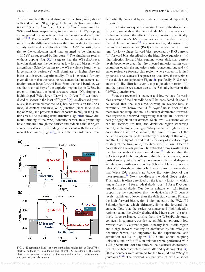
2012 to simulate the band structure of the InAs/WSe2 diode
with and without NO2 doping. Hole and electron concentra-
tions of 5 � 1015cm�3 and 1.5 � 1018cm�3 were used for
WSe2 and InAs, respectively, in the absence of NO2 doping,
as suggested by reports of their respective undoped thin
films.20,27 The WSe2/Pd Schottky barrier height was deter-
mined by the difference between the semiconductor electron
affinity and metal work function. The InAs/Pd Schottky bar-
rier to the conduction band was assumed to be pinned at
�0.15 eV as suggested by literature.28 The simulation results
without doping (Fig. 3(a)) suggest that the WSe2/InAs p-n
junction dominates the behavior at low forward biases, while
a significant Schottky barrier to the WSe2 valence band (i.e., a
large parasitic resistance) will dominate at higher forward
biases as observed experimentally. This is expected for any
given diode in that the parasitic resistances lead to current sat-
uration under large forward bias. From the band bending, we
see that the majority of the depletion region lies in WSe2. In
order to simulate the band structure under NO2 doping, a
highly doped WSe2 layer (Na¼ 1 � 1019cm�3)24 was intro-
duced as shown in the inset of Figure 3(b). As discussed previ-
ously, it is assumed that the NO2 has no effects on the InAs,
InAs/Pd contact, and InAs/WSe2 junction (since InAs is on
top of WSe2 and protects it from exposure to NO2 in the junc-
tion area). The resulting band structure (Fig. 3(b)) shows dra-
matic thinning of the WSe2 Schottky barrier, thus promoting
hole tunneling through the barrier and reducing the WSe2/Pd
contact resistance. This finding is consistent with the experi-
mental I-V curves (Fig. 2(b)), where the forward bias current
is drastically enhanced by �3 orders of magnitude upon NO2
exposure.
In addition to a quantitative simulation of the diode band
diagram, we analyze the heterodiode I-V characteristics to
further understand the effect of each junction. Specifically,
a standard diode’s I-V characteristics can be described by
five different regimes:29 (i) reverse-bias, dominated by
recombination-generation (R-G) current as well as drift cur-
rent; (ii) low-voltage forward-bias, governed by R-G current;
(iii) forward-bias, described by the ideal diode equations; (iv)
high-injection forward-bias region, where diffusion current
levels become so great that the injected minority carrier con-
centration equals the majority carrier concentration; and (v)
series-resistance forward-bias region, where current is limited
by parasitic resistances. The processes that drive these regimes
in our device are depicted in Figure 3: specifically, R-G mech-
anisms (i, ii), diffusion over the p-n junction barrier (iii),
and the parasitic resistance due to the Schottky barrier of the
Pd/WSe2 junction (v).
First, the reverse-bias current and low-voltage forward-
bias current of the heterodiode will be considered. It should
be noted that the measured current in reverse-bias is
extremely low, below the 10�12 A/lm2 noise floor of the
measurement setup, and no R-G current dominated forward-
bias regime is observed, suggesting that the RG current is
nearly negligible in our devices. Such low RG current values
can be ascribed to: first, the depletion region occurring
entirely in the higher bandgap WSe2 due to the higher carrier
concentration in InAs; second, the small volume of the
depletion region due to the relatively thin body of the WSe2;
and third, it is hypothesized that the density of interface traps
existing at the InAs/WSe2 interface must be low. Electron
concentration levels previously extracted from similar InAs
membranes without intentional doping20 indicate that the
InAs is doped high enough such that the depletion region is
pushed mostly into the WSe2, as shown in the band diagram
simulations. Furthermore, WSe2 Schottky FETs previously
fabricated also show extremely low off currents, suggesting
that WSe2 R-G currents are below the noise floor of our
measurements.24 Next, we discuss the ideal diode region.
This region is often described by the ideality factor, g, which
ranges from g¼ 1 for an ideal diode to g¼ 2 for a R-G cur-
rent dominated diode. Our device exhibits g¼ 1.1, further
supporting the conclusion that the device has R-G current
levels significantly lower than the diffusion current. Finally,
the high forward bias region is dominated by the WSe2/Pd
Schottky barrier, which ultimately limits the forward-bias
current. Note that the series resistance and high injection
regimes cannot be clearly distinguished here given the rela-
tively large resistance arising from the WSe2/Pd Schottky
contacts. In summary, our device exhibits an extremely low
reverse bias RG current region, a nearly ideal diode region
and a high forward bias region dominated by the WSe2/Pd
Schottky barrier, also supported by the experimental and
simulation results in Figure 4. 2D simulations coupling
Poisson’s and drift diffusion relations were performed with
TCAD Sentaurus 2012 to analyze the electrical characteris-
tics of the heterostructure diode after NO2 doping (Fig. 4).
Ohmic contacts were assumed for the InAs/Pd and WSe2/Pd
junctions.24,25 The forward current was fit with a series
FIG. 3. Electrostatic band structure simulation results for an InAs/WSe2
stack (a) without NO2 gas doping and (b) with NO2 gas doping. The insets
show cross sectional schematics of the simulated structures. Important cur-
rent processes are also shown.
242101-3 Chuang et al. Appl. Phys. Lett. 102, 242101 (2013)
Reuse of AIP Publishing content is subject to the terms at: https://publishing.aip.org/authors/rights-and-permissions. Download to IP: 130.126.153.83 On: Sun, 14 Aug 2016
00:02:31
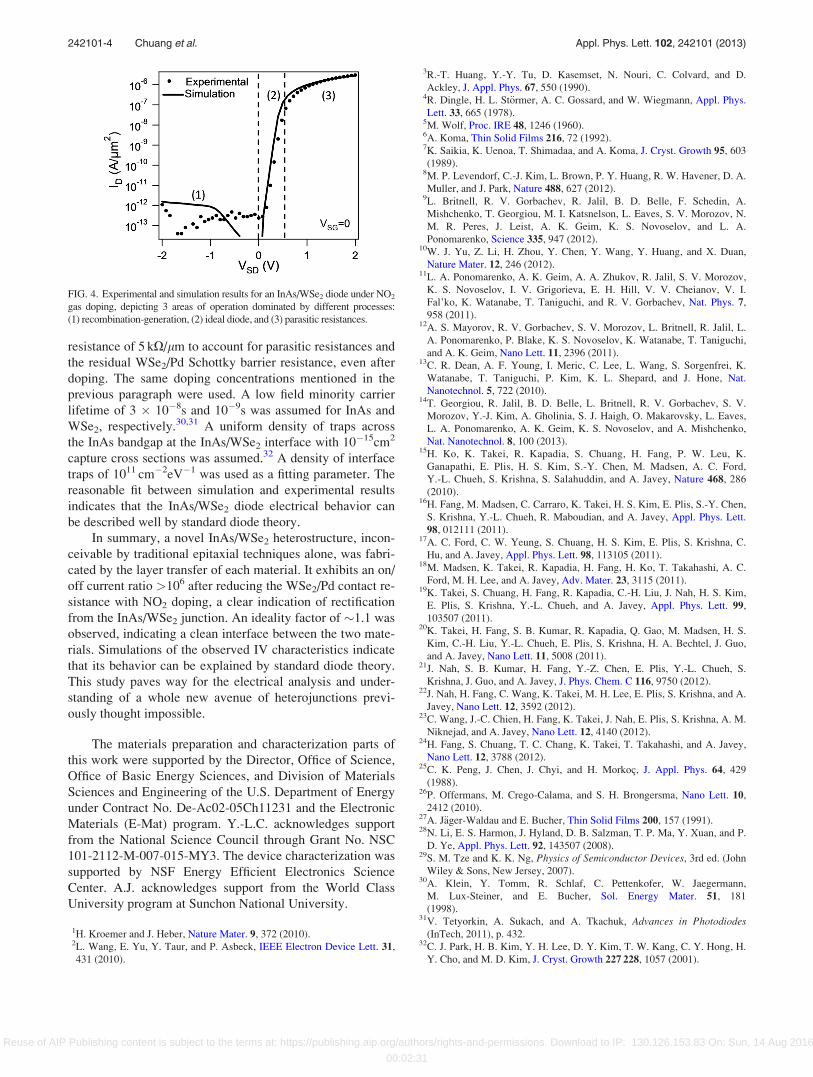
resistance of 5 kX/lm to account for parasitic resistances and
the residual WSe2/Pd Schottky barrier resistance, even after
doping. The same doping concentrations mentioned in the
previous paragraph were used. A low field minority carrier
lifetime of 3 � 10�8s and 10�9s was assumed for InAs and
WSe2, respectively.30,31 A uniform density of traps across
the InAs bandgap at the InAs/WSe2 interface with 10�15cm2
capture cross sections was assumed.32 A density of interface
traps of 1011 cm�2eV�1 was used as a fitting parameter. The
reasonable fit between simulation and experimental results
indicates that the InAs/WSe2 diode electrical behavior can
be described well by standard diode theory.
In summary, a novel InAs/WSe2 heterostructure, incon-
ceivable by traditional epitaxial techniques alone, was fabri-
cated by the layer transfer of each material. It exhibits an on/
off current ratio >106 after reducing the WSe2/Pd contact re-
sistance with NO2 doping, a clear indication of rectification
from the InAs/WSe2 junction. An ideality factor of �1.1 was
observed, indicating a clean interface between the two mate-
rials. Simulations of the observed IV characteristics indicate
that its behavior can be explained by standard diode theory.
This study paves way for the electrical analysis and under-
standing of a whole new avenue of heterojunctions previ-
ously thought impossible.
The materials preparation and characterization parts of
this work were supported by the Director, Office of Science,
Office of Basic Energy Sciences, and Division of Materials
Sciences and Engineering of the U.S. Department of Energy
under Contract No. De-Ac02-05Ch11231 and the Electronic
Materials (E-Mat) program. Y.-L.C. acknowledges support
from the National Science Council through Grant No. NSC
101-2112-M-007-015-MY3. The device characterization was
supported by NSF Energy Efficient Electronics Science
Center. A.J. acknowledges support from the World Class
University program at Sunchon National University.
1H. Kroemer and J. Heber, Nature Mater. 9, 372 (2010).2L. Wang, E. Yu, Y. Taur, and P. Asbeck, IEEE Electron Device Lett. 31,
431 (2010).
3R.-T. Huang, Y.-Y. Tu, D. Kasemset, N. Nouri, C. Colvard, and D.
Ackley, J. Appl. Phys. 67, 550 (1990).4R. Dingle, H. L. St€ormer, A. C. Gossard, and W. Wiegmann, Appl. Phys.
Lett. 33, 665 (1978).5M. Wolf, Proc. IRE 48, 1246 (1960).6A. Koma, Thin Solid Films 216, 72 (1992).7K. Saikia, K. Uenoa, T. Shimadaa, and A. Koma, J. Cryst. Growth 95, 603
(1989).8M. P. Levendorf, C.-J. Kim, L. Brown, P. Y. Huang, R. W. Havener, D. A.
Muller, and J. Park, Nature 488, 627 (2012).9L. Britnell, R. V. Gorbachev, R. Jalil, B. D. Belle, F. Schedin, A.
Mishchenko, T. Georgiou, M. I. Katsnelson, L. Eaves, S. V. Morozov, N.
M. R. Peres, J. Leist, A. K. Geim, K. S. Novoselov, and L. A.
Ponomarenko, Science 335, 947 (2012).10W. J. Yu, Z. Li, H. Zhou, Y. Chen, Y. Wang, Y. Huang, and X. Duan,
Nature Mater. 12, 246 (2012).11L. A. Ponomarenko, A. K. Geim, A. A. Zhukov, R. Jalil, S. V. Morozov,
K. S. Novoselov, I. V. Grigorieva, E. H. Hill, V. V. Cheianov, V. I.
Fal’ko, K. Watanabe, T. Taniguchi, and R. V. Gorbachev, Nat. Phys. 7,
958 (2011).12A. S. Mayorov, R. V. Gorbachev, S. V. Morozov, L. Britnell, R. Jalil, L.
A. Ponomarenko, P. Blake, K. S. Novoselov, K. Watanabe, T. Taniguchi,
and A. K. Geim, Nano Lett. 11, 2396 (2011).13C. R. Dean, A. F. Young, I. Meric, C. Lee, L. Wang, S. Sorgenfrei, K.
Watanabe, T. Taniguchi, P. Kim, K. L. Shepard, and J. Hone, Nat.
Nanotechnol. 5, 722 (2010).14T. Georgiou, R. Jalil, B. D. Belle, L. Britnell, R. V. Gorbachev, S. V.
Morozov, Y.-J. Kim, A. Gholinia, S. J. Haigh, O. Makarovsky, L. Eaves,
L. A. Ponomarenko, A. K. Geim, K. S. Novoselov, and A. Mishchenko,
Nat. Nanotechnol. 8, 100 (2013).15H. Ko, K. Takei, R. Kapadia, S. Chuang, H. Fang, P. W. Leu, K.
Ganapathi, E. Plis, H. S. Kim, S.-Y. Chen, M. Madsen, A. C. Ford,
Y.-L. Chueh, S. Krishna, S. Salahuddin, and A. Javey, Nature 468, 286
(2010).16H. Fang, M. Madsen, C. Carraro, K. Takei, H. S. Kim, E. Plis, S.-Y. Chen,
S. Krishna, Y.-L. Chueh, R. Maboudian, and A. Javey, Appl. Phys. Lett.
98, 012111 (2011).17A. C. Ford, C. W. Yeung, S. Chuang, H. S. Kim, E. Plis, S. Krishna, C.
Hu, and A. Javey, Appl. Phys. Lett. 98, 113105 (2011).18M. Madsen, K. Takei, R. Kapadia, H. Fang, H. Ko, T. Takahashi, A. C.
Ford, M. H. Lee, and A. Javey, Adv. Mater. 23, 3115 (2011).19K. Takei, S. Chuang, H. Fang, R. Kapadia, C.-H. Liu, J. Nah, H. S. Kim,
E. Plis, S. Krishna, Y.-L. Chueh, and A. Javey, Appl. Phys. Lett. 99,
103507 (2011).20K. Takei, H. Fang, S. B. Kumar, R. Kapadia, Q. Gao, M. Madsen, H. S.
Kim, C.-H. Liu, Y.-L. Chueh, E. Plis, S. Krishna, H. A. Bechtel, J. Guo,
and A. Javey, Nano Lett. 11, 5008 (2011).21J. Nah, S. B. Kumar, H. Fang, Y.-Z. Chen, E. Plis, Y.-L. Chueh, S.
Krishna, J. Guo, and A. Javey, J. Phys. Chem. C 116, 9750 (2012).22J. Nah, H. Fang, C. Wang, K. Takei, M. H. Lee, E. Plis, S. Krishna, and A.
Javey, Nano Lett. 12, 3592 (2012).23C. Wang, J.-C. Chien, H. Fang, K. Takei, J. Nah, E. Plis, S. Krishna, A. M.
Niknejad, and A. Javey, Nano Lett. 12, 4140 (2012).24H. Fang, S. Chuang, T. C. Chang, K. Takei, T. Takahashi, and A. Javey,
Nano Lett. 12, 3788 (2012).25C. K. Peng, J. Chen, J. Chyi, and H. Morkoc, J. Appl. Phys. 64, 429
(1988).26P. Offermans, M. Crego-Calama, and S. H. Brongersma, Nano Lett. 10,
2412 (2010).27A. J€ager-Waldau and E. Bucher, Thin Solid Films 200, 157 (1991).28N. Li, E. S. Harmon, J. Hyland, D. B. Salzman, T. P. Ma, Y. Xuan, and P.
D. Ye, Appl. Phys. Lett. 92, 143507 (2008).29S. M. Tze and K. K. Ng, Physics of Semiconductor Devices, 3rd ed. (John
Wiley & Sons, New Jersey, 2007).30A. Klein, Y. Tomm, R. Schlaf, C. Pettenkofer, W. Jaegermann,
M. Lux-Steiner, and E. Bucher, Sol. Energy Mater. 51, 181
(1998).31V. Tetyorkin, A. Sukach, and A. Tkachuk, Advances in Photodiodes
(InTech, 2011), p. 432.32C. J. Park, H. B. Kim, Y. H. Lee, D. Y. Kim, T. W. Kang, C. Y. Hong, H.
Y. Cho, and M. D. Kim, J. Cryst. Growth 227 228, 1057 (2001).
FIG. 4. Experimental and simulation results for an InAs/WSe2 diode under NO2
gas doping, depicting 3 areas of operation dominated by different processes:
(1) recombination-generation, (2) ideal diode, and (3) parasitic resistances.
242101-4 Chuang et al. Appl. Phys. Lett. 102, 242101 (2013)
Reuse of AIP Publishing content is subject to the terms at: https://publishing.aip.org/authors/rights-and-permissions. Download to IP: 130.126.153.83 On: Sun, 14 Aug 2016
00:02:31