Embed Size (px)
Citation preview

© Semiconductor Components Industries, LLC, 2015
January, 2015 − Rev. 11 Publication Order Number:
NCL30081/D
NCL30081
Dimmable Quasi-ResonantPrimary Side Current-ModeController for LED Lighting
The NCL30081 is a PWM current mode controller targeting isolatedflyback and non−isolated constant current topologies. The controlleroperates in a quasi−resonant mode to provide high efficiency. Thanksto a novel control method, the device is able to precisely regulate aconstant LED current from the primary side. This removes the needfor secondary side feedback circuitry, biasing and an optocoupler.
The device is highly integrated with a minimum number of externalcomponents. A robust suite of safety protection is built in to simplifythe design. This device is specifically intended for very compact spaceefficient designs. It supports step dimming by monitoring the AC lineand detecting when the line has been toggled on−off−on by the user toreduce the light intensity in 5 steps down to 5% dimming.
Features
• Quasi−resonant Peak Current−mode Control Operation
• Primary Side Sensing (no optocoupler needed)
• Wide VCC Range
• Precise LED Constant Current Regulation ±1% Typical
• Line Feed−forward for Enhanced Regulation Accuracy
• Low LED Current Ripple
• 250 mV ±2% Guaranteed Voltage Reference for Current Regulation
• ~ 0.9 Power Factor with Valley Fill Input Stage
• Low Start−up Current (10 �A typ.)
• Small Space Saving Low Profile Package
• 5 State Quasi−log Dimmable
• Wide Temperature Range of −40 to +125°C
• Pb−free, Halide−free MSL1 Product
• Robust Protection Features♦ Over Voltage / LED Open Circuit Protection♦ Secondary Diode Short Protection♦ Output Short Circuit Protection♦ Shorted Current Sense Pin Fault Detection♦ Latched and Auto−recoverable Versions♦ Brown−out♦ VCC Under Voltage Lockout♦ Thermal Shutdown
Typical Applications• Integral LED Bulbs
• LED Power Driver Supplies
• LED Light Engines
www.onsemi.com
PIN CONNECTIONS
See detailed ordering and shipping information in the packagedimensions section on page 30 of this data sheet.
ORDERING INFORMATION
TSOP−6SN SUFFIXCASE 318G
MARKING DIAGRAM
VIN
VCC
DRV
ZCD
GND
CS
(Top View)
1
1
AAx = Specific Device Codex = G or HA = Assembly LocationY = YearW = Work Week� = Pb−Free Package
AAxAYW�
�
1
(Note: Microdot may be in either location)

NCL30081
www.onsemi.com2
Figure 1. Typical Application Schematic for NCL30081
Aux
1
2
3 4
5
6
.
.
.
Table 1. PIN FUNCTION DESCRIPTION
Pin No Pin Name Function Pin Description
1 ZCD Zero Crossing Detection Connected to the auxiliary winding, this pin detects the core reset event.
2 GND − The controller ground
3 CS Current sense This pin monitors the primary peak current
4 DRV Driver output The current capability of the totem pole gate drive (+0.3/−0.5 A) makes it suit-able to effectively drive a broad range of power MOSFETs.
5 VCC Supplies the controller This pin is connected to an external auxiliary voltage.
6 VIN Input voltage sensingBrown−Out
This pin observes the HV rail and is used in valley selection. This pin alsomonitors and protects for low mains conditions.
NCL30081
www.onsemi.com3
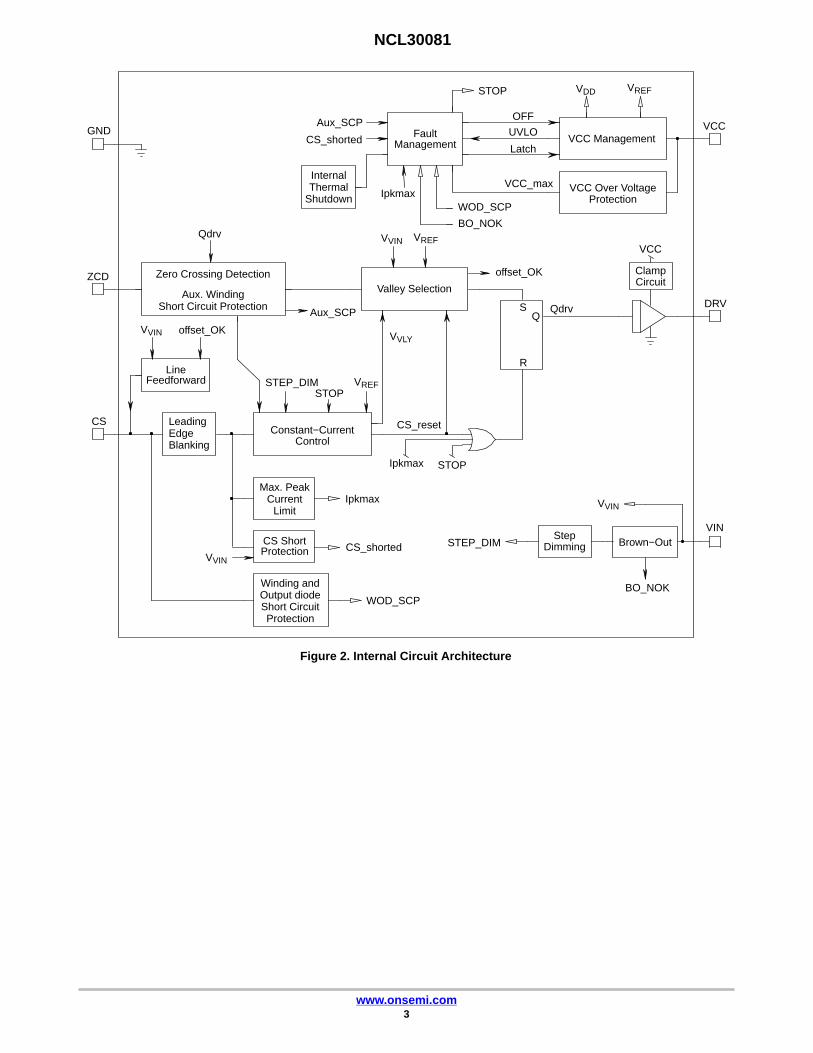
Figure 2. Internal Circuit Architecture
ZCD Zero Crossing Detection
CS LeadingEdgeBlanking
Winding andOutput diodeShort CircuitProtection
Max. PeakCurrent
LimitIpkmax
WOD_SCP
Qdrv
VCC ManagementVCC
DRV
VCC
InternalThermal
Shutdown
ClampCircuit
VINBrown−OutDimmingSTEP_DIM
BO_NOK
CS_reset
STOP
UVLO
OFF
Latch
STOP
WOD_SCPIpkmax
BO_NOK
GND
STOP
Qdrv
STEP_DIM
Short Circuit ProtectionAux_SCP
Aux_SCP
VCC_max
offset_OK
offset_OK
Line
Ipkmax
CS ShortProtection CS_shorted
CS_shorted
Valley Selection
Fault
Constant−CurrentControl
Step
Feedforward
Aux. Winding
Management
ProtectionVCC Over Voltage
S
R
Q
VVIN
VVIN
VVIN
VREF
VREF
VVLY
VVIN
VREFVDD
NCL30081
www.onsemi.com4
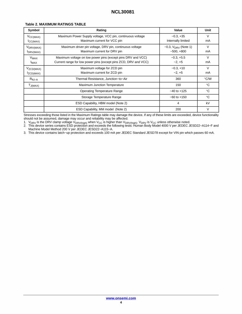
Table 2. MAXIMUM RATINGS TABLE
Symbol Rating Value Unit
VCC(MAX)
ICC(MAX)
Maximum Power Supply voltage, VCC pin, continuous voltageMaximum current for VCC pin
−0.3, +35Internally limited
VmA
VDRV(MAX)
IDRV(MAX)
Maximum driver pin voltage, DRV pin, continuous voltageMaximum current for DRV pin
−0.3, VDRV (Note 1)−500, +800
VmA
VMAX
IMAX
Maximum voltage on low power pins (except pins DRV and VCC)Current range for low power pins (except pins ZCD, DRV and VCC)
−0.3, +5.5−2, +5
VmA
VZCD(MAX)
IZCD(MAX)
Maximum voltage for ZCD pinMaximum current for ZCD pin
−0.3, +10−2, +5
VmA
RθJ−A Thermal Resistance, Junction−to−Air 360 °C/W
TJ(MAX) Maximum Junction Temperature 150 °C
Operating Temperature Range −40 to +125 °C
Storage Temperature Range −60 to +150 °C
ESD Capability, HBM model (Note 2) 4 kV
ESD Capability, MM model (Note 2) 200 V
Stresses exceeding those listed in the Maximum Ratings table may damage the device. If any of these limits are exceeded, device functionalityshould not be assumed, damage may occur and reliability may be affected.1. VDRV is the DRV clamp voltage VDRV(high) when VCC is higher than VDRV(high). VDRV is VCC unless otherwise noted.2. This device series contains ESD protection and exceeds the following tests: Human Body Model 4000 V per JEDEC JESD22−A114−F and
Machine Model Method 200 V per JEDEC JESD22−A115−A.3. This device contains latch−up protection and exceeds 100 mA per JEDEC Standard JESD78 except for VIN pin which passes 60 mA.
NCL30081
www.onsemi.com5
Table 3. ELECTRICAL CHARACTERISTICS (Unless otherwise noted: For typical values TJ = 25°C, VCC = 12 V;For min/max values TJ = −40°C to +125°C, Max TJ = 150°C, VCC = 12 V)
Description Test Condition Symbol Min Typ Max Unit
STARTUP AND SUPPLY CIRCUITS
Supply VoltageStartup ThresholdMinimum Operating VoltageHysteresis VCC(on) – VCC(off)
Internal logic reset
VCC increasingVCC decreasingVCC decreasing
VCC(on)
VCC(off)
VCC(HYS)
VCC(reset)
168.28
3.5
188.8–
4.5
209.4–
5.5
V
Over Voltage ProtectionVCC OVP threshold
VCC(OVP) 26 28 30 V
VCC(off) noise filterVCC(reset) noise filter−
tVCC(off)
tVCC(reset)
––
520
––
�s
Startup current ICC(start) – 13 30 �A
Startup current in fault mode ICC(sFault) – 46 60 �A
Supply CurrentDevice Disabled/FaultDevice Enabled/No output load on pin 5Device Switching (Fsw = 65 kHz)
VCC > VCC(off)
Fsw = 65 kHzCDRV = 470 pF,Fsw = 65 kHz
ICC1
ICC2
ICC3
0.8––
1.02.152.6
1.44.05.0
mA
CURRENT SENSE
Maximum Internal current limit VILIM 0.95 1 1.05 V
Leading Edge Blanking Duration for VILIM(Tj = −25°C to 125°C)
tLEB 250 300 350 ns
Leading Edge Blanking Duration for VILIM(Tj = −40°C to 125°C)
tLEB 240 300 350 ns
Input Bias Current DRV high Ibias – 0.02 – �A
Propagation delay from current detection to gate off−state tILIM – 50 150 ns
Threshold for immediate fault protection activation VCS(stop) 1.35 1.5 1.65 V
Leading Edge Blanking Duration for VCS(stop) tBCS – 120 – ns
Blanking time for CS to GND short detection VpinVIN = 1 V tCS(blank1) 8.0 – 14.0 �s
Blanking time for CS to GND short detection VpinVIN = 3.3 V tCS(blank2) 2.6 – 4.6 �s
GATE DRIVE
Drive ResistanceDRV SinkDRV Source
RSNKRSRC
––
1330
––
�
Drive current capabilityDRV Sink (Note 4)DRV Source (Note 4)
ISNKISRC
––
500300
––
mA
Rise Time (10% to 90%) CDRV = 470 pF tr – 40 – ns
Fall Time (90% to 10%) CDRV = 470 pF tf – 30 – ns
DRV Low Voltage VCC = VCC(off)+0.2 VCDRV = 470 pF,RDRV = 33 k�
VDRV(low) 8 – – V
DRV High Voltage VCC = 30 VCDRV = 470 pF,RDRV = 33 k�
VDRV(high) 10 12 14 V
4. Guaranteed by design
NCL30081
www.onsemi.com6
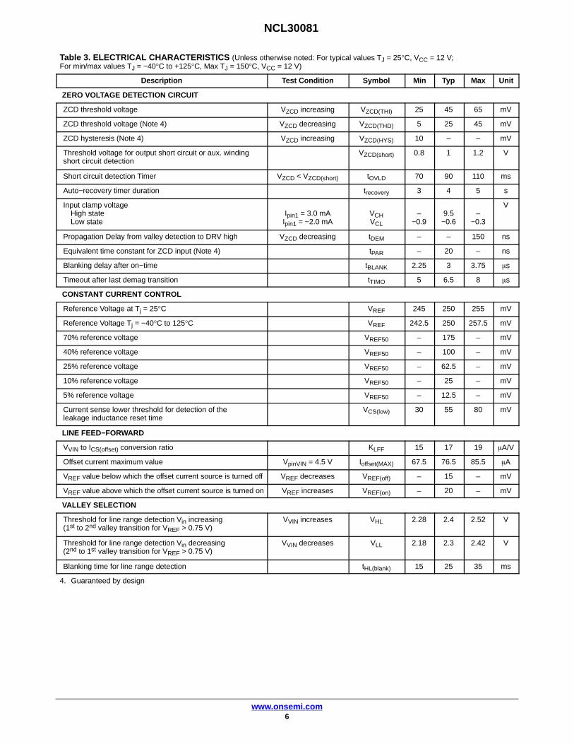
Table 3. ELECTRICAL CHARACTERISTICS (Unless otherwise noted: For typical values TJ = 25°C, VCC = 12 V;For min/max values TJ = −40°C to +125°C, Max TJ = 150°C, VCC = 12 V)
Description UnitMaxTypMinSymbolTest Condition
ZERO VOLTAGE DETECTION CIRCUIT
ZCD threshold voltage VZCD increasing VZCD(THI) 25 45 65 mV
ZCD threshold voltage (Note 4) VZCD decreasing VZCD(THD) 5 25 45 mV
ZCD hysteresis (Note 4) VZCD increasing VZCD(HYS) 10 – – mV
Threshold voltage for output short circuit or aux. windingshort circuit detection
VZCD(short) 0.8 1 1.2 V
Short circuit detection Timer VZCD < VZCD(short) tOVLD 70 90 110 ms
Auto−recovery timer duration trecovery 3 4 5 s
Input clamp voltageHigh stateLow state
Ipin1 = 3.0 mAIpin1 = −2.0 mA
VCHVCL
–−0.9
9.5−0.6
–−0.3
V
Propagation Delay from valley detection to DRV high VZCD decreasing tDEM – – 150 ns
Equivalent time constant for ZCD input (Note 4) tPAR – 20 – ns
Blanking delay after on−time tBLANK 2.25 3 3.75 �s
Timeout after last demag transition tTIMO 5 6.5 8 �s
CONSTANT CURRENT CONTROL
Reference Voltage at Tj = 25°C VREF 245 250 255 mV
Reference Voltage Tj = −40°C to 125°C VREF 242.5 250 257.5 mV
70% reference voltage VREF50 – 175 – mV
40% reference voltage VREF50 – 100 – mV
25% reference voltage VREF50 – 62.5 – mV
10% reference voltage VREF50 – 25 – mV
5% reference voltage VREF50 – 12.5 – mV
Current sense lower threshold for detection of theleakage inductance reset time
VCS(low) 30 55 80 mV
LINE FEED−FORWARD
VVIN to ICS(offset) conversion ratio KLFF 15 17 19 �A/V
Offset current maximum value VpinVIN = 4.5 V Ioffset(MAX) 67.5 76.5 85.5 �A
VREF value below which the offset current source is turned off VREF decreases VREF(off) – 15 – mV
VREF value above which the offset current source is turned on VREF increases VREF(on) – 20 – mV
VALLEY SELECTION
Threshold for line range detection Vin increasing (1st to 2nd valley transition for VREF > 0.75 V)
VVIN increases VHL 2.28 2.4 2.52 V
Threshold for line range detection Vin decreasing (2nd to 1st valley transition for VREF > 0.75 V)
VVIN decreases VLL 2.18 2.3 2.42 V
Blanking time for line range detection tHL(blank) 15 25 35 ms
4. Guaranteed by design
NCL30081
www.onsemi.com7
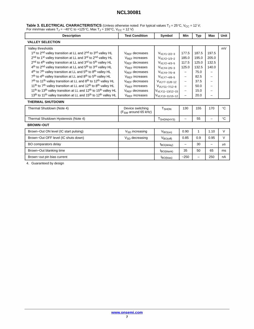
Table 3. ELECTRICAL CHARACTERISTICS (Unless otherwise noted: For typical values TJ = 25°C, VCC = 12 V;For min/max values TJ = −40°C to +125°C, Max TJ = 150°C, VCC = 12 V)
Description UnitMaxTypMinSymbolTest Condition
VALLEY SELECTION
Valley thresholds1st to 2nd valley transition at LL and 2nd to 3rd valley HL2nd to 1st valley transition at LL and 3rd to 2nd valley HL2nd to 4th valley transition at LL and 3rd to 5th valley HL4th to 2nd valley transition at LL and 5th to 3rd valley HL4th to 7th valley transition at LL and 5th to 8th valley HL7th to 4th valley transition at LL and 8th to 5th valley HL7th to 11th valley transition at LL and 8th to 12th valley HL11th to 7th valley transition at LL and 12th to 8th valley HL11th to 13th valley transition at LL and 12th to 15th valley HL13th to 11th valley transition at LL and 15th to 12th valley HL
VREF decreasesVREF increasesVREF decreasesVREF increasesVREF decreasesVREF increasesVREF decreasesVREF increasesVREF decreasesVREF increases
VVLY1−2/2−3
VVLY2−1/3−2
VVLY2−4/3−5
VVLY4−2/5−3
VVLY4−7/5−8
VVLY7−4/8−5
VVLY7−11/8−12
VVLY11−7/12−8
VVLY11−13/12−15
VVLY13−11/15−12
177.5185.0117.5125.0
––––––
187.5195.0125.0132.575.082.537.550.015.020.0
197.5205.0132.5140.0
––––––
mV
THERMAL SHUTDOWN
Thermal Shutdown (Note 4) Device switching(FSW around 65 kHz)
TSHDN 130 155 170 °C
Thermal Shutdown Hysteresis (Note 4) TSHDN(HYS) – 55 – °C
BROWN−OUT
Brown−Out ON level (IC start pulsing) VSD increasing VBO(on) 0.90 1 1.10 V
Brown−Out OFF level (IC shuts down) VSD decreasing VBO(off) 0.85 0.9 0.95 V
BO comparators delay tBO(delay) – 30 – �s
Brown−Out blanking time tBO(blank) 35 50 65 ms
Brown−out pin bias current IBO(bias) −250 – 250 nA
4. Guaranteed by design
NCL30081
www.onsemi.com8
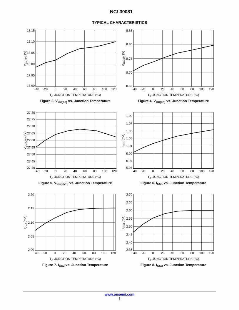
TYPICAL CHARACTERISTICS
Figure 3. VCC(on) vs. Junction Temperature Figure 4. VCC(off) vs. Junction Temperature
TJ, JUNCTION TEMPERATURE (°C) TJ, JUNCTION TEMPERATURE (°C)
100806040200−20−4017.90
17.95
18.00
18.05
18.10
18.15
8.65
8.70
8.75
8.80
8.85
Figure 5. VCC(OVP) vs. Junction Temperature Figure 6. ICC1 vs. Junction Temperature
TJ, JUNCTION TEMPERATURE (°C) TJ, JUNCTION TEMPERATURE (°C)
27.40
27.55
27.60
27.65
27.70
27.75
27.80
0.95
0.97
0.99
1.01
1.03
1.05
1.07
1.09
Figure 7. ICC2 vs. Junction Temperature Figure 8. ICC3 vs. Junction Temperature
TJ, JUNCTION TEMPERATURE (°C) TJ, JUNCTION TEMPERATURE (°C)
2.00
2.05
2.10
2.15
2.20
2.35
2.40
2.50
2.55
2.60
2.65
2.70
VC
C(o
n) (
V)
VC
C(o
ff) (
V)
VC
C(O
VP
) (V
)
I CC
1 (m
A)
I CC
2 (m
A)
I CC
3 (m
A)
120 100806040200−20−40 120
100806040200−20−40 120 100806040200−20−40 120
100806040200−20−40 120 100806040200−20−40 120
2.45
27.50
27.45
NCL30081
www.onsemi.com9
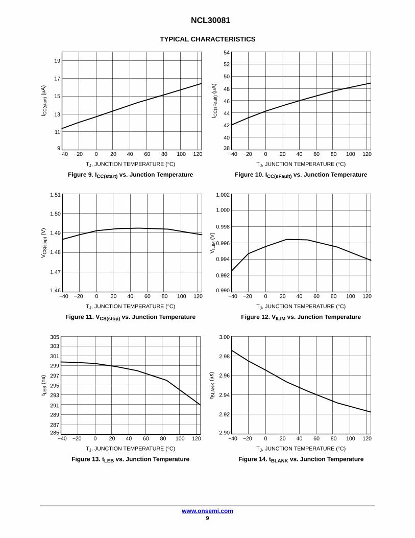
TYPICAL CHARACTERISTICS
Figure 9. ICC(start) vs. Junction Temperature Figure 10. ICC(sFault) vs. Junction Temperature
TJ, JUNCTION TEMPERATURE (°C) TJ, JUNCTION TEMPERATURE (°C)
100806040200−20−409
11
13
15
17
19
38
40
42
44
48
50
52
54
Figure 11. VCS(stop) vs. Junction Temperature Figure 12. VILIM vs. Junction Temperature
TJ, JUNCTION TEMPERATURE (°C) TJ, JUNCTION TEMPERATURE (°C)
1.46
1.47
1.49
1.50
1.51
0.990
0.992
0.996
1.000
1.002
Figure 13. tLEB vs. Junction Temperature Figure 14. tBLANK vs. Junction Temperature
TJ, JUNCTION TEMPERATURE (°C) TJ, JUNCTION TEMPERATURE (°C)
285287
291
293
295
299
303
305
2.90
2.92
2.94
2.96
2.98
3.00
I CC
(sta
rt) (�A
)
I CC
(sF
ault)
(�A
)
VC
S(s
top)
(V
)
VIL
IM (
V)
t LE
B (
ns)
t BLA
NK (�s)
120 100806040200−20−40 120
100806040200−20−40 120 100806040200−20−40 120
100806040200−20−40 120 100806040200−20−40 120
46
289
297
301
1.480.994
0.998
NCL30081
www.onsemi.com10
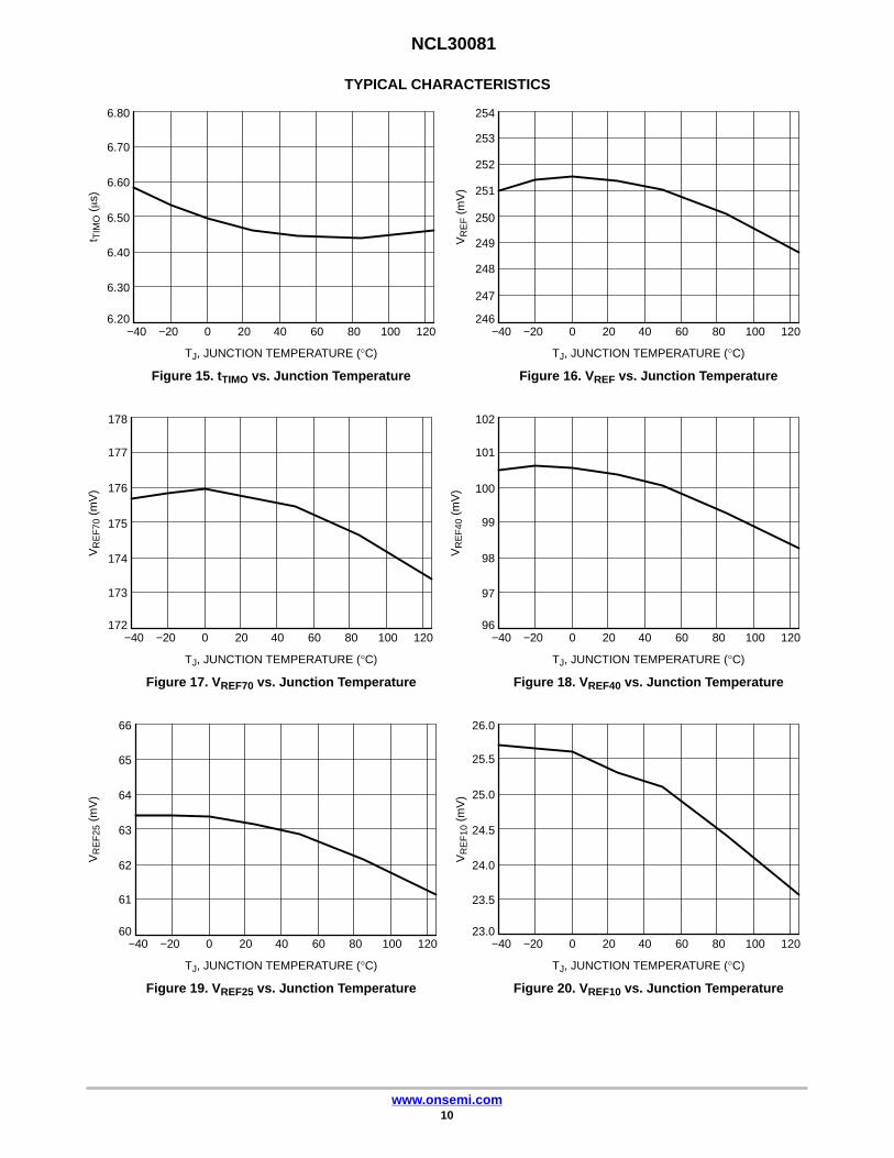
TYPICAL CHARACTERISTICS
Figure 15. tTIMO vs. Junction Temperature Figure 16. VREF vs. Junction Temperature
TJ, JUNCTION TEMPERATURE (°C) TJ, JUNCTION TEMPERATURE (°C)
100806040200−20−406.20
6.30
6.50
6.70
6.80
246
247
248
250
251
253
254
Figure 17. VREF70 vs. Junction Temperature Figure 18. VREF40 vs. Junction Temperature
TJ, JUNCTION TEMPERATURE (°C) TJ, JUNCTION TEMPERATURE (°C)
172
173
175
177
178
96
97
98
100
101
102
Figure 19. VREF25 vs. Junction Temperature Figure 20. VREF10 vs. Junction Temperature
TJ, JUNCTION TEMPERATURE (°C) TJ, JUNCTION TEMPERATURE (°C)
60
61
62
63
64
65
66
23.0
23.5
24.5
25.0
26.0
t TIM
O (�s)
VR
EF (
mV
)
VR
EF
70 (
mV
)
VR
EF
40 (
mV
)
VR
EF
25 (
mV
)
VR
EF
10 (
mV
)
120 100806040200−20−40 120
100806040200−20−40 120 100806040200−20−40 120
100806040200−20−40 120 100806040200−20−40 120
6.40
6.60
249
252
174
176
99
24.0
25.5
NCL30081
www.onsemi.com11
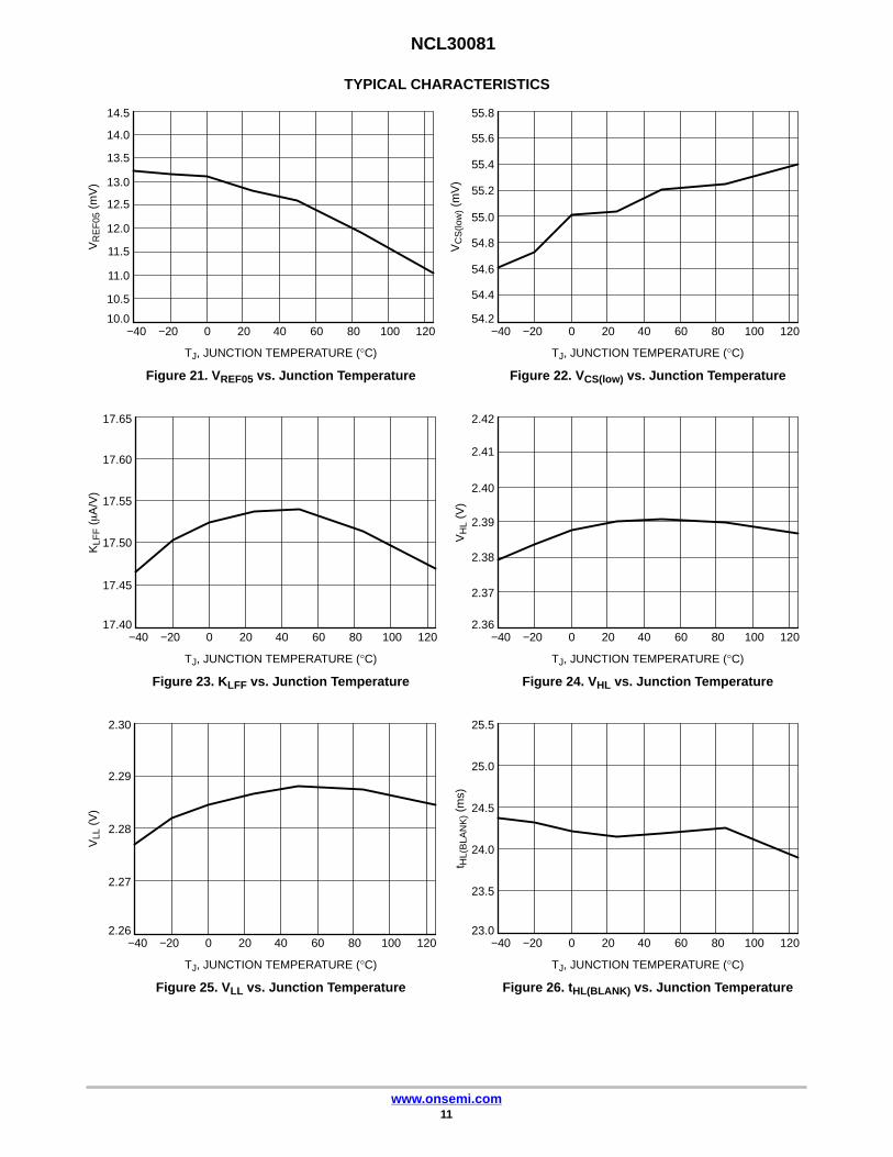
TYPICAL CHARACTERISTICS
Figure 21. VREF05 vs. Junction Temperature Figure 22. VCS(low) vs. Junction Temperature
TJ, JUNCTION TEMPERATURE (°C) TJ, JUNCTION TEMPERATURE (°C)
100806040200−20−4010.0
13.0
14.0
14.5
54.2
54.4
54.8
55.2
55.4
55.8
Figure 23. KLFF vs. Junction Temperature Figure 24. VHL vs. Junction Temperature
TJ, JUNCTION TEMPERATURE (°C) TJ, JUNCTION TEMPERATURE (°C)
17.40
17.45
17.50
17.60
17.65
2.36
2.37
2.41
2.42
Figure 25. VLL vs. Junction Temperature Figure 26. tHL(BLANK) vs. Junction Temperature
TJ, JUNCTION TEMPERATURE (°C) TJ, JUNCTION TEMPERATURE (°C)
2.26
2.29
2.30
23.0
23.5
24.0
24.5
25.0
25.5
VR
EF
05 (
mV
)
VC
S(lo
w) (
mV
)
KLF
F (�A
/V)
VH
L (V
)
VLL
(V
)
t HL(
BLA
NK
) (m
s)
120 100806040200−20−40 120
100806040200−20−40 120 100806040200−20−40 120
100806040200−20−40 120 100806040200−20−40 120
11.0
12.0
2.38
2.39
2.40
2.27
2.28
10.5
13.5
11.5
12.5
54.6
55.0
55.6
17.55
NCL30081
www.onsemi.com12
TYPICAL CHARACTERISTICS
Figure 27. VVLY1−2/2−3 vs. JunctionTemperature
Figure 28. VVLY2−1/3−2 vs. JunctionTemperature
TJ, JUNCTION TEMPERATURE (°C) TJ, JUNCTION TEMPERATURE (°C)
100806040200−20−40185.0
186.2
186.4
186.8
192
193
195
197
198
200
Figure 29. VVLY2−4/3−5 vs. JunctionTemperature
Figure 30. VVLY4−2/5−3 vs. JunctionTemperature
TJ, JUNCTION TEMPERATURE (°C) TJ, JUNCTION TEMPERATURE (°C)
123.4
123.6
124.0
124.4
124.6
130
131
133
136
137
Figure 31. VVLY4−7/5−8 vs. JunctionTemperature
Figure 32. VVLY7−4/8−5 vs. JunctionTemperature
TJ, JUNCTION TEMPERATURE (°C) TJ, JUNCTION TEMPERATURE (°C)
74.0
74.2
74.8
75.0
80
81
82
83
85
86
87
88
VV
LY1−
2/2−
3 (m
V)
VV
LY2−
1/3−
2 (m
V)
VV
LY2−
4/3−
5 (m
V)
VV
LY4−
2/5−
3 (m
V)
VV
LY4−
7/5−
8 (m
V)
VV
LY7−
4/8−
5 (m
V)
120 100806040200−20−40 120
100806040200−20−40 120 100806040200−20−40 120
100806040200−20−40 120 100806040200−20−40 120
185.4
186.6
132
134
135
74.4
74.6
185.2
185.6
185.8
186.0
194
196
199
123.8
124.2
84
NCL30081
www.onsemi.com13
TYPICAL CHARACTERISTICS
Figure 33. VVLY7−11/8−12 vs. JunctionTemperature
Figure 34. VVLY11−7/12−8 vs. JunctionTemperature
TJ, JUNCTION TEMPERATURE (°C) TJ, JUNCTION TEMPERATURE (°C)
100806040200−20−4036.7
37.0
37.1
37.3
43
44
46
47
48
50
Figure 35. VVLY11−13/12−15 vs. JunctionTemperature
Figure 36. VVLY13−11/15−12 vs. JunctionTemperature
TJ, JUNCTION TEMPERATURE (°C) TJ, JUNCTION TEMPERATURE (°C)
12.6
13.1
14.1
15.1
15.6
17.5
18.0
19.0
20.5
21.0
Figure 37. VBO(on) vs. Junction Temperature Figure 38. VBO(off) vs. Junction Temperature
TJ, JUNCTION TEMPERATURE (°C) TJ, JUNCTION TEMPERATURE (°C)
0.975
0.985
0.990
0.995
1.000
0.890
0.895
0.900
0.905
0.910
VV
LY7−
11/8
−12
(mV
)
VV
LY11
−7/1
2−8
(mV
)
VV
LY11
−13/
12−1
5 (m
V)
VV
LY13
−11/
15−1
2 (m
V)
VB
O(o
n) (
V)
VB
O(o
ff) (
V)
120 100806040200−20−40 120
100806040200−20−40 120 100806040200−20−40 120
100806040200−20−40 120 100806040200−20−40 120
36.8
36.9
18.5
19.5
20.0
0.980
37.2
45
49
13.6
14.6
NCL30081
www.onsemi.com14
TYPICAL CHARACTERISTICS
Figure 39. tBO(BLANK) vs. JunctionTemperature
Figure 40. tOVLD vs. Junction Temperature
TJ, JUNCTION TEMPERATURE (°C) TJ, JUNCTION TEMPERATURE (°C)
100806040200−20−4050.0
52.0
52.5
53.5
80.5
81.5
82.5
83.0
84.0
85.0
Figure 41. trecovery vs. Junction Temperature
TJ, JUNCTION TEMPERATURE (°C)
4.05
4.15
4.20
4.30
4.40
t BO
(BLA
NK
) (m
s)
t OV
LD (
ms)
t reco
very
(s)
120 100806040200−20−40 120
100806040200−20−40 120
50.5
51.0
51.5
53.0
81.0
82.0
83.5
84.5
4.10
4.25
4.35
NCL30081
www.onsemi.com15
Application Information
The NCL30081 implements a current−mode architectureoperating in quasi−resonant mode. Thanks to proprietarycircuitry, the controller is able to accurately regulate thesecondary side current of the flyback converter withoutusing any opto−coupler or measuring directly the secondaryside current.• Quasi−Resonance Current−Mode Operation:
implementing quasi−resonance operation in peakcurrent−mode control, the NCL30081 optimizes theefficiency by switching in the valley of the MOSFETdrain−source voltage. Thanks to a smart controlalgorithm, the controller locks−out in a selected valleyand remains locked until the input voltage or the outputcurrent set point significantly changes.
• Primary Side Constant Current Control: thanks to aproprietary circuit, the controller is able to compensatefor the leakage inductance of the transformer and allowaccurate control of the secondary side current.
• Line Feed−forward: compensation for possiblevariation of the output current caused by system slewrate variation.
• Open LED protection: if the voltage on the VCC pinexceeds an internal limit, the controller shuts down andwaits 4 seconds before restarting switching.
• Brown−Out: the controller includes a brown−outcircuit with a validation timer which safely stops thecontroller in the event that the input voltage is too low.The device will automatically restart if the line recovers.
• Cycle−by−cycle peak current limit: when the currentsense voltage exceeds the internal threshold VILIM, theMOSFET is turned off for the rest of the switching cycle.
• Winding Short−Circuit Protection: an additionalcomparator with a short LEB filter (tBCS) senses the CSsignal and stops the controller if VCS reaches 1.5 xVILIM. For noise immunity reasons, this comparator isenabled only during the main LEB duration tLEB.
• Output Short−circuit protection: If a very lowvoltage is applied on ZCD pin for 90 ms (nominal), thecontrollers assume that the output or the ZCD pin isshorted to ground and enters shutdown. The auto−restart version (B suffix) waits 4 seconds, then thecontroller restarts switching. In the latched version (Asuffix), the controller is latched as long as VCC staysabove the VCC(reset) threshold.
• Step dimming: Each time the IC detects a brown−outcondition, the output current is decreased by discrete steps.
NCL30081
www.onsemi.com16
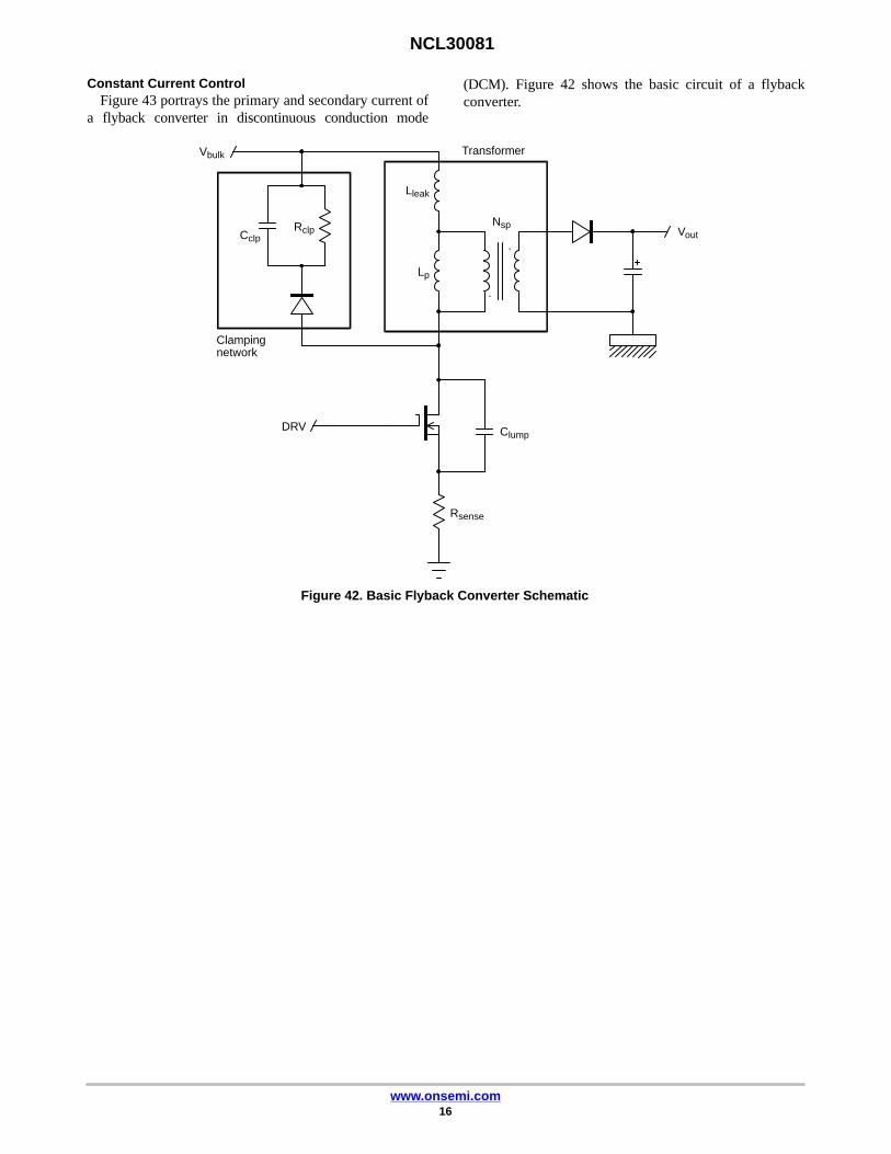
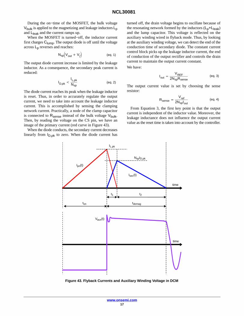
Constant Current ControlFigure 43 portrays the primary and secondary current of
a flyback converter in discontinuous conduction mode
(DCM). Figure 42 shows the basic circuit of a flybackconverter.
.
.
DRV
Clampingnetwork
Transformer
Figure 42. Basic Flyback Converter Schematic
Clump
Rsense
VoutNsp
Lp
Lleak
Vbulk
CclpRclp
NCL30081
www.onsemi.com17
During the on−time of the MOSFET, the bulk voltageVbulk is applied to the magnetizing and leakage inductors Lpand Lleak and the current ramps up.
When the MOSFET is turned−off, the inductor currentfirst charges Clump. The output diode is off until the voltageacross Lp reverses and reaches:
Nsp�Vout � Vf� (eq. 1)
The output diode current increase is limited by the leakageinductor. As a consequence, the secondary peak current isreduced:
ID,pk �IL,pk
Nsp(eq. 2)
The diode current reaches its peak when the leakage inductoris reset. Thus, in order to accurately regulate the outputcurrent, we need to take into account the leakage inductorcurrent. This is accomplished by sensing the clampingnetwork current. Practically, a node of the clamp capacitoris connected to Rsense instead of the bulk voltage Vbulk.Then, by reading the voltage on the CS pin, we have animage of the primary current (red curve in Figure 43).
When the diode conducts, the secondary current decreaseslinearly from ID,pk to zero. When the diode current has
turned off, the drain voltage begins to oscillate because ofthe resonating network formed by the inductors (Lp+Lleak)and the lump capacitor. This voltage is reflected on theauxiliary winding wired in flyback mode. Thus, by lookingat the auxiliary winding voltage, we can detect the end of theconduction time of secondary diode. The constant currentcontrol block picks up the leakage inductor current, the endof conduction of the output rectifier and controls the draincurrent to maintain the output current constant.
We have:
Iout �VREF
2NspRsense(eq. 3)
The output current value is set by choosing the senseresistor:
Rsense �Vref
2NspIout(eq. 4)
From Equation 3, the first key point is that the outputcurrent is independent of the inductor value. Moreover, theleakage inductance does not influence the output currentvalue as the reset time is taken into account by the controller.
time
time
Figure 43. Flyback Currents and Auxiliary Winding Voltage in DCM
Vaux(t)
ton tdemag
t1 t2
Isec(t)
Ipri(t)
NspID,pk
IL,pk
NCL30081
www.onsemi.com18
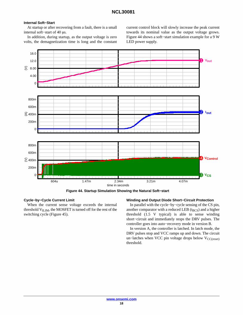
Internal Soft−StartAt startup or after recovering from a fault, there is a small
internal soft−start of 40 �s.In addition, during startup, as the output voltage is zero
volts, the demagnetization time is long and the constant
current control block will slowly increase the peak currenttowards its nominal value as the output voltage grows.Figure 44 shows a soft−start simulation example for a 9 WLED power supply.
Figure 44. Startup Simulation Showing the Natural Soft−start
0
4.00
8.00
12.0
16.0
1
0
200m
400m
600m
800m
2
604u 1.47m 2.34m 3.21mtime in seconds
4.07m
0
200m
400m
600m
800m
3
4
Iout
VCS
Vout
VControl
(A)
(V)
(V)
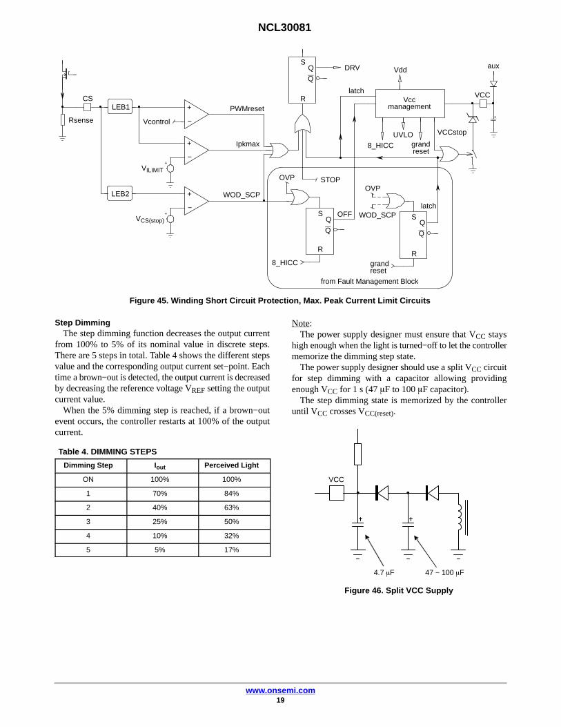
Cycle−by−Cycle Current LimitWhen the current sense voltage exceeds the internal
threshold VILIM, the MOSFET is turned off for the rest of theswitching cycle (Figure 45).
Winding and Output Diode Short−Circuit ProtectionIn parallel with the cycle−by−cycle sensing of the CS pin,
another comparator with a reduced LEB (tBCS) and a higherthreshold (1.5 V typical) is able to sense windingshort−circuit and immediately stops the DRV pulses. Thecontroller goes into auto−recovery mode in version B.
In version A, the controller is latched. In latch mode, theDRV pulses stop and VCC ramps up and down. The circuitun−latches when VCC pin voltage drops below VCC(reset)threshold.
NCL30081
www.onsemi.com19
Figure 45. Winding Short Circuit Protection, Max. Peak Current Limit Circuits
S
R
Q
CS
Rsense
LEB1 +
−
S
R
Q
VCC
aux
Vccmanagement
Vdd
grandreset
DRV
Ipkmax
PWMreset
VCCstop
+
−
LEB2 WOD_SCP
Vcontrol
+
−
STOP
from Fault Management Block
OVP
UVLO
S
R
Q
grandreset
OVP
8_HICC
OFF WOD_SCP
latch
latch
8_HICC
VILIMIT
VCS(stop)
Q
Q
Q
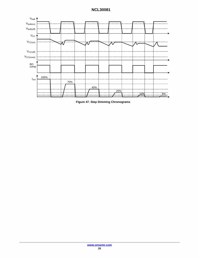
Step DimmingThe step dimming function decreases the output current
from 100% to 5% of its nominal value in discrete steps.There are 5 steps in total. Table 4 shows the different stepsvalue and the corresponding output current set−point. Eachtime a brown−out is detected, the output current is decreasedby decreasing the reference voltage VREF setting the outputcurrent value.
When the 5% dimming step is reached, if a brown−outevent occurs, the controller restarts at 100% of the outputcurrent.
Table 4. DIMMING STEPS
Dimming Step Iout Perceived Light
ON 100% 100%
1 70% 84%
2 40% 63%
3 25% 50%
4 10% 32%
5 5% 17%
Note:The power supply designer must ensure that VCC stays
high enough when the light is turned−off to let the controllermemorize the dimming step state.
The power supply designer should use a split VCC circuitfor step dimming with a capacitor allowing providingenough VCC for 1 s (47 �F to 100 �F capacitor).
The step dimming state is memorized by the controlleruntil VCC crosses VCC(reset).
VCC
4.7 �F
Figure 46. Split VCC Supply
47 − 100 �F
NCL30081
www.onsemi.com20
70%
BOcomp
100%
40%25%
10% 5%
Figure 47. Step Dimming Chronograms
Iout
VCC(reset)
VCC(off)
VCC(on)
VCC
Vbulk(off)
Vbulk(on)
Vbulk

NCL30081
www.onsemi.com21
VCC Over Voltage Protection (Open LED Protection)If no output load is connected to the LED power supply,
the controller must be able to safely limit the output voltageexcursion.
In the NCL30081, when the VCC voltage reaches theVCC(OVP) threshold, the controller stops the DRV pulses andthe 4−s timer starts counting. The IC re−start switching afterthe 4−s timer has elapsed as long as VCC ≥ VCC(on). This isillustrated in Figure 48.
Figure 48. Open LED Protection Chronograms
0
10.0
20.0
30.0
40.0
1
0
10.0
20.0
30.0
40.0
2
0
200m
400m
600m
800m
3
1.38 3.96 6.54 9.11 11.7time in seconds
0
2.00
4.00
6.00
8.00
4
VCC(on)
VCC(OVP)
VCC(off)
Vout
Iout
VCC
OVP
(V)
(A)
(V)
(V)
Valley LockoutQuasi−Square wave resonant systems have a wide
switching frequency excursion. The switching frequencyincreases when the output load decreases or when the inputvoltage increases. The switching frequency of such systemsmust be limited.
The NCL30081 changes valley as the input voltageincreases and as the output current set−point is varied(thermal fold−back and step dimming). This limits theswitching frequency excursion. Once a valley is selected,the controller stays locked in the valley until the input
voltage or the output current set−point varies significantly.This avoids valley jumping and the inherent noise caused bythis phenomenon.
The input voltage is sensed by the VIN pin. The internallogic selects the operating valley according to VIN pinvoltage (Figure 49) and the dimming state imposed by theStep Dimming feature.
By default, when the output current is not dimmed, thecontroller operates in the first valley at low line and in thesecond valley at high line.
NCL30081
www.onsemi.com22
+
−
Vbulk
VINLLine
25−ms blanking timeHLine
2.4 V if LLine low2.3 V if LLine high
Figure 49. Line Range Detection
Table 5. VALLEY SELECTION
Iout value at which thecontroller changes valley
(Iout decreasing)
VIN pin voltage for valley change
Iout value at which thecontroller changes valley
(Iout increasing)
VVIN decreases
0 −LL− 2.3 V −HL− 5 V
I out
dec
reas
es
100%1st 2nd 100%
Iout increases
75% 78%2nd 3rd
50% 53%4th 5th
30% 33%7th 8th
15% 20%11th 12th
6% 8%
13th 15th0% 0%
0 −LL− 2.4 V −HL− 5 V
VVIN increases
VIN pin voltage for valley change
NCL30081
www.onsemi.com23
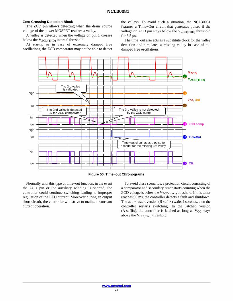
Zero Crossing Detection BlockThe ZCD pin allows detecting when the drain−source
voltage of the power MOSFET reaches a valley.A valley is detected when the voltage on pin 1 crosses
below the VZCD(THD) internal threshold.At startup or in case of extremely damped free
oscillations, the ZCD comparator may not be able to detect
the valleys. To avoid such a situation, the NCL30081features a Time−Out circuit that generates pulses if thevoltage on ZCD pin stays below the VZCD(THD) thresholdfor 6.5 �s.
The time−out also acts as a substitute clock for the valleydetection and simulates a missing valley in case of toodamped free oscillations.
Figure 50. Time−out Chronograms
43
14
12
15
16
17
low
high
Clk
TimeOut
low
high
low
high
low
high
ZCD comp
2nd,
VZCD
The 3rd valley is not detectedby the ZCD comp
Time−out circuit adds a pulse toaccount for the missing 3rd valley
The 2nd valley is detectedBy the ZCD comparator
VZCD(THD)
The 3rd valleyis validated
3rd
Normally with this type of time−out function, in the eventthe ZCD pin or the auxiliary winding is shorted, thecontroller could continue switching leading to improperregulation of the LED current. Moreover during an outputshort circuit, the controller will strive to maintain constantcurrent operation.
To avoid these scenarios, a protection circuit consisting ofa comparator and secondary timer starts counting when theZCD voltage is below the VZCD(short) threshold. If this timerreaches 90 ms, the controller detects a fault and shutdown.The auto−restart version (B suffix) waits 4 seconds, then thecontroller restarts switching. In the latched version(A suffix), the controller is latched as long as VCC staysabove the VCC(reset) threshold.
NCL30081
www.onsemi.com24
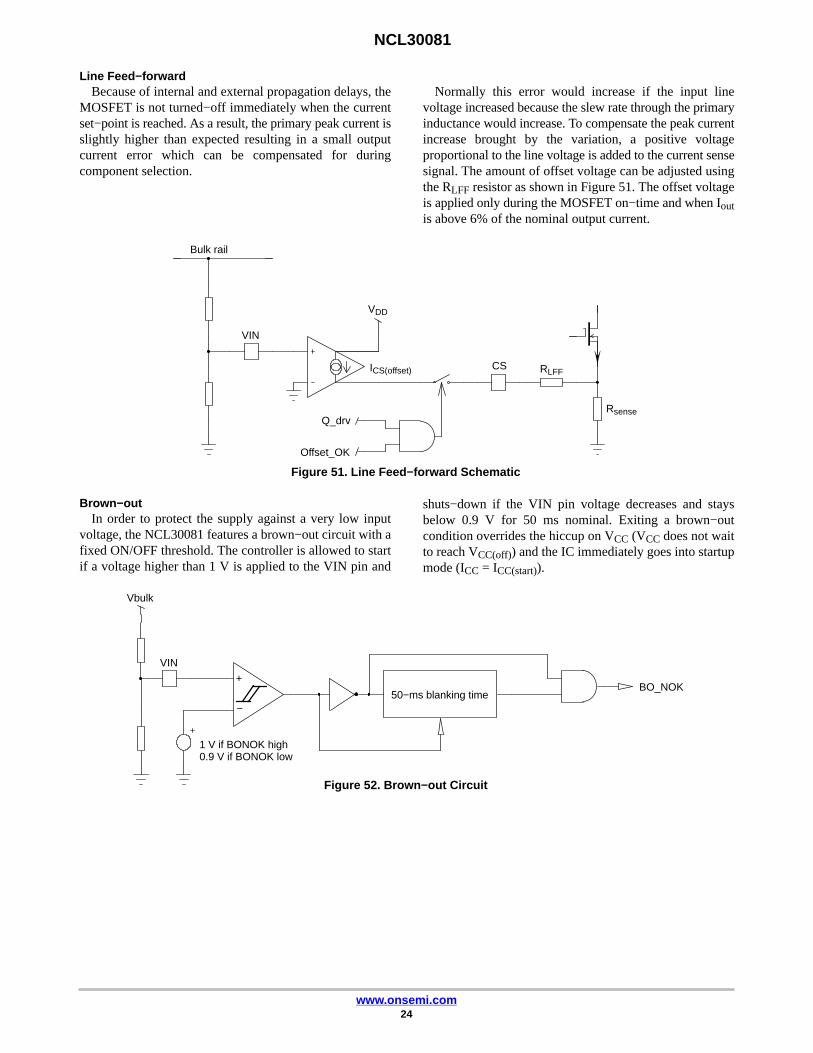
Line Feed−forwardBecause of internal and external propagation delays, the
MOSFET is not turned−off immediately when the currentset−point is reached. As a result, the primary peak current isslightly higher than expected resulting in a small outputcurrent error which can be compensated for duringcomponent selection.
Normally this error would increase if the input linevoltage increased because the slew rate through the primaryinductance would increase. To compensate the peak currentincrease brought by the variation, a positive voltageproportional to the line voltage is added to the current sensesignal. The amount of offset voltage can be adjusted usingthe RLFF resistor as shown in Figure 51. The offset voltageis applied only during the MOSFET on−time and when Ioutis above 6% of the nominal output current.
Bulk rail
VIN
CS
Q_drv
Offset_OK
Figure 51. Line Feed−forward Schematic
VDD
ICS(offset) RLFF
Rsense
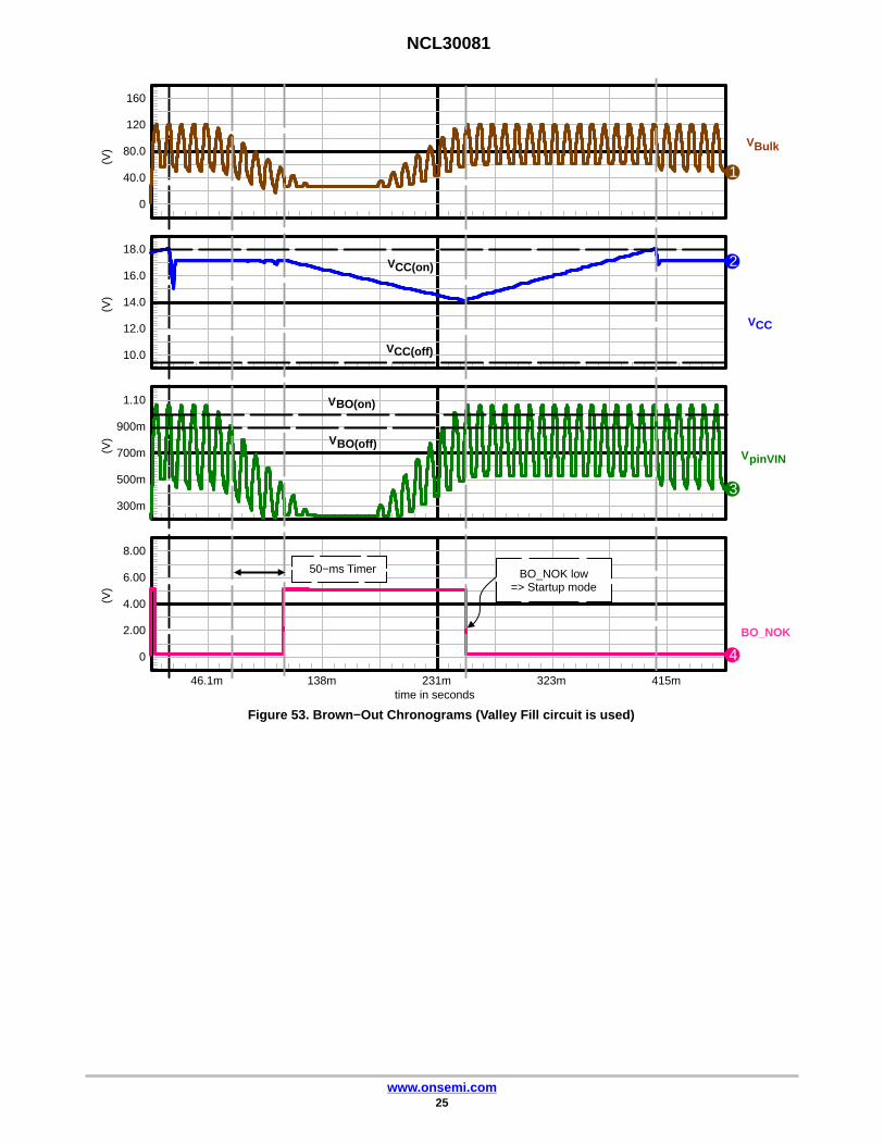
Brown−outIn order to protect the supply against a very low input
voltage, the NCL30081 features a brown−out circuit with afixed ON/OFF threshold. The controller is allowed to startif a voltage higher than 1 V is applied to the VIN pin and
shuts−down if the VIN pin voltage decreases and staysbelow 0.9 V for 50 ms nominal. Exiting a brown−outcondition overrides the hiccup on VCC (VCC does not waitto reach VCC(off)) and the IC immediately goes into startupmode (ICC = ICC(start)).
+
−
Vbulk
VIN
BO_NOK50−ms blanking time
1 V if BONOK high0.9 V if BONOK low
Figure 52. Brown−out Circuit
NCL30081
www.onsemi.com25
Figure 53. Brown−Out Chronograms (Valley Fill circuit is used)
0
40.0
80.0
120
160
1
10.0
12.0
14.0
16.0
18.02
300m
500m
700m
900m
1.10
3
46.1m 138m 231m 323m 415mtime in seconds
0
2.00
4.00
6.00
8.00
4
VCC
VBulk
VpinVIN
BO_NOK
(V)
(V)
(V)
(V)
BO_NOK low=> Startup mode
50−ms Timer
VBO(on)
VBO(off)
VCC(on)
VCC(off)
NCL30081
www.onsemi.com26
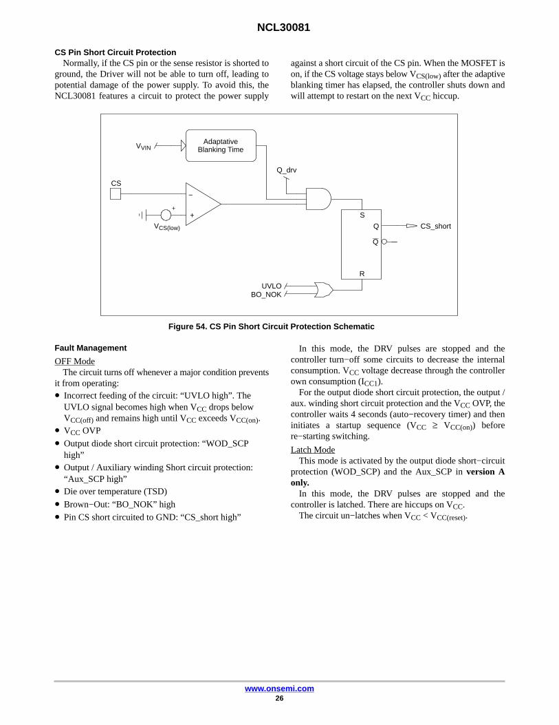
CS Pin Short Circuit ProtectionNormally, if the CS pin or the sense resistor is shorted to
ground, the Driver will not be able to turn off, leading topotential damage of the power supply. To avoid this, theNCL30081 features a circuit to protect the power supply
against a short circuit of the CS pin. When the MOSFET ison, if the CS voltage stays below VCS(low) after the adaptiveblanking timer has elapsed, the controller shuts down andwill attempt to restart on the next VCC hiccup.
+
−
CS
Q_drv
CS_short
S
R
Q
UVLOBO_NOK
AdaptativeBlanking Time
Figure 54. CS Pin Short Circuit Protection Schematic
Q
VCS(low)
VVIN
Fault Management
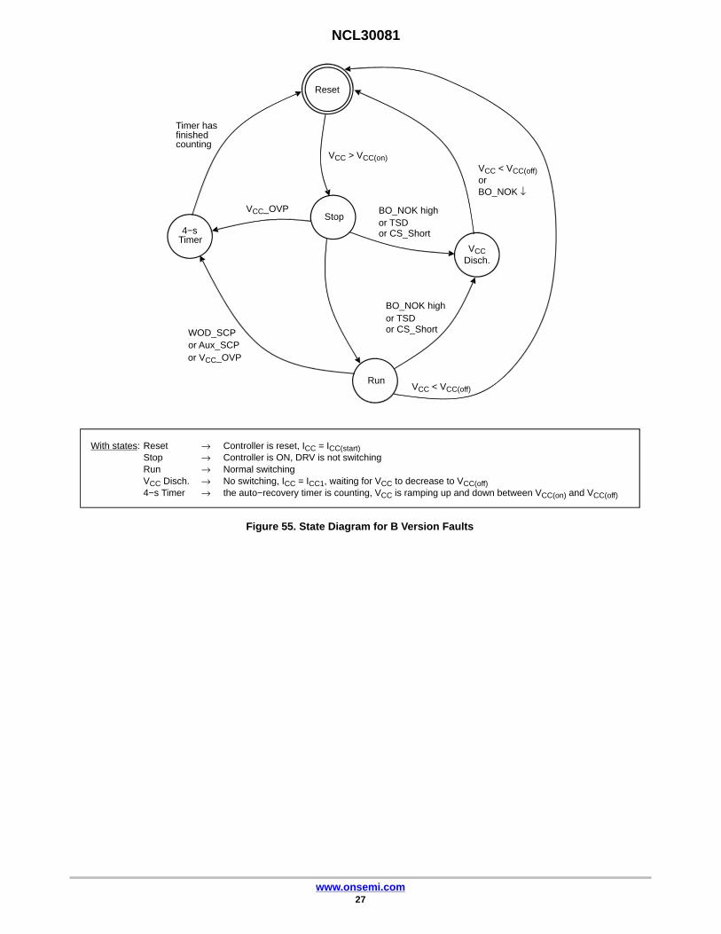
OFF ModeThe circuit turns off whenever a major condition prevents
it from operating:• Incorrect feeding of the circuit: “UVLO high”. The
UVLO signal becomes high when VCC drops belowVCC(off) and remains high until VCC exceeds VCC(on).
• VCC OVP
• Output diode short circuit protection: “WOD_SCPhigh”
• Output / Auxiliary winding Short circuit protection:“Aux_SCP high”
• Die over temperature (TSD)
• Brown−Out: “BO_NOK” high
• Pin CS short circuited to GND: “CS_short high”
In this mode, the DRV pulses are stopped and thecontroller turn−off some circuits to decrease the internalconsumption. VCC voltage decrease through the controllerown consumption (ICC1).
For the output diode short circuit protection, the output /aux. winding short circuit protection and the VCC OVP, thecontroller waits 4 seconds (auto−recovery timer) and theninitiates a startup sequence (VCC ≥ VCC(on)) beforere−starting switching.
Latch ModeThis mode is activated by the output diode short−circuit
protection (WOD_SCP) and the Aux_SCP in version Aonly.
In this mode, the DRV pulses are stopped and thecontroller is latched. There are hiccups on VCC.
The circuit un−latches when VCC < VCC(reset).
NCL30081
www.onsemi.com27
Reset
Stop
4−sTimer
Run
BO_NOK highor TSDor CS_Short
WOD_SCPor Aux_SCP
Timer hasfinishedcounting
BO_NOK highor TSDor CS_Short
Figure 55. State Diagram for B Version Faults
or VCC_OVP
VCC > VCC(on)
VCC < VCC(off)
VCCDisch.
VCC < VCC(off)orBO_NOK ↓
VCC_OVP
With states: ResetStopRunVCC Disch.4−s Timer
→→→→→
Controller is reset, ICC = ICC(start)Controller is ON, DRV is not switchingNormal switchingNo switching, ICC = ICC1, waiting for VCC to decrease to VCC(off)the auto−recovery timer is counting, VCC is ramping up and down between VCC(on) and VCC(off)

NCL30081
www.onsemi.com28
Figure 56. State Diagram for A Version Faults
With states: ResetStopRunVCC Disch.4−s TimerLatch
→→→→→→
Controller is reset, ICC = ICC(start)Controller is ON, DRV is not switchingNormal switchingNo switching, ICC = ICC1, waiting for VCC to decrease to VCC(off)the auto−recovery timer is counting, VCC is ramping up and down between VCC(on) and VCC(off)Controller is latched off, VCC is ramping up and down between VCC(on) and VCC(off),only VCC(reset) can release the latch.
Reset
Stop4−sTimer
Run
BO_NOK highor TSDor CS_Short
Latch
WOD_SCP orAux_SCP
Timer hasfinishedcounting
BO_NOK highor TSDor CS_Short
VCC > VCC(on)
VCC < VCC(off)
VCCDisch.
VCC < VCC(off)orBO_NOK ↓
VCC_OVP
VCC < VCC(reset)
VCC_OVP

ÉÉÉÉ
TSOP−6CASE 318G−02
ISSUE VDATE 12 JUN 2012SCALE 2:1
STYLE 1:PIN 1. DRAIN
2. DRAIN3. GATE4. SOURCE5. DRAIN6. DRAIN
2 3
456
D
1
eb
E1
A1
A0.05
NOTES:1. DIMENSIONING AND TOLERANCING PER ASME Y14.5M, 1994.2. CONTROLLING DIMENSION: MILLIMETERS.3. MAXIMUM LEAD THICKNESS INCLUDES LEAD FINISH. MINIMUM
LEAD THICKNESS IS THE MINIMUM THICKNESS OF BASE MATERIAL.4. DIMENSIONS D AND E1 DO NOT INCLUDE MOLD FLASH,
PROTRUSIONS, OR GATE BURRS. MOLD FLASH, PROTRUSIONS, ORGATE BURRS SHALL NOT EXCEED 0.15 PER SIDE. DIMENSIONS DAND E1 ARE DETERMINED AT DATUM H.
5. PIN ONE INDICATOR MUST BE LOCATED IN THE INDICATED ZONE.
c
STYLE 2:PIN 1. EMITTER 2
2. BASE 13. COLLECTOR 14. EMITTER 15. BASE 26. COLLECTOR 2
STYLE 3:PIN 1. ENABLE
2. N/C3. R BOOST4. Vz5. V in6. V out
STYLE 4:PIN 1. N/C
2. V in3. NOT USED4. GROUND5. ENABLE6. LOAD
XXX M�
�
XXX = Specific Device CodeA =Assembly LocationY = YearW = Work Week� = Pb−Free Package
STYLE 5:PIN 1. EMITTER 2
2. BASE 23. COLLECTOR 14. EMITTER 15. BASE 16. COLLECTOR 2
STYLE 6:PIN 1. COLLECTOR
2. COLLECTOR3. BASE4. EMITTER5. COLLECTOR6. COLLECTOR
STYLE 7:PIN 1. COLLECTOR
2. COLLECTOR3. BASE4. N/C5. COLLECTOR6. EMITTER
STYLE 8:PIN 1. Vbus
2. D(in)3. D(in)+4. D(out)+5. D(out)6. GND
GENERICMARKING DIAGRAM*
STYLE 9:PIN 1. LOW VOLTAGE GATE
2. DRAIN3. SOURCE4. DRAIN5. DRAIN6. HIGH VOLTAGE GATE
STYLE 10:PIN 1. D(OUT)+
2. GND3. D(OUT)−4. D(IN)−5. VBUS6. D(IN)+
1
1
*For additional information on our Pb−Free strategy and solderingdetails, please download the ON Semiconductor Soldering andMounting Techniques Reference Manual, SOLDERRM/D.
SOLDERING FOOTPRINT*
STYLE 11:PIN 1. SOURCE 1
2. DRAIN 23. DRAIN 24. SOURCE 25. GATE 16. DRAIN 1/GATE 2
STYLE 12:PIN 1. I/O
2. GROUND3. I/O4. I/O5. VCC6. I/O
*This information is generic. Please refer to device data sheetfor actual part marking. Pb−Free indicator, “G” or microdot “�”, may or may not be present.
XXXAYW�
�
1
STANDARDIC
XXX = Specific Device CodeM = Date Code� = Pb−Free Package
DIMA
MIN NOM MAXMILLIMETERS
0.90 1.00 1.10A1 0.01 0.06 0.10b 0.25 0.38 0.50c 0.10 0.18 0.26D 2.90 3.00 3.10E 2.50 2.75 3.00
e 0.85 0.95 1.05L 0.20 0.40 0.60
0.25 BSCL2−0° 10°
STYLE 13:PIN 1. GATE 1
2. SOURCE 23. GATE 24. DRAIN 25. SOURCE 16. DRAIN 1
STYLE 14:PIN 1. ANODE
2. SOURCE3. GATE4. CATHODE/DRAIN5. CATHODE/DRAIN6. CATHODE/DRAIN
STYLE 15:PIN 1. ANODE
2. SOURCE3. GATE4. DRAIN5. N/C6. CATHODE
1.30 1.50 1.70E1
E
RECOMMENDED
NOTE 5
LCM
H
L2
SEATINGPLANE
GAUGEPLANE
DETAIL Z
DETAIL Z
0.606X
3.200.956X
0.95PITCH
DIMENSIONS: MILLIMETERS
M
STYLE 16:PIN 1. ANODE/CATHODE
2. BASE3. EMITTER4. COLLECTOR5. ANODE6. CATHODE
STYLE 17:PIN 1. EMITTER
2. BASE3. ANODE/CATHODE4. ANODE5. CATHODE6. COLLECTOR
MECHANICAL CASE OUTLINE
PACKAGE DIMENSIONS
ON Semiconductor and are trademarks of Semiconductor Components Industries, LLC dba ON Semiconductor or its subsidiaries in the United States and/or other countries.ON Semiconductor reserves the right to make changes without further notice to any products herein. ON Semiconductor makes no warranty, representation or guarantee regardingthe suitability of its products for any particular purpose, nor does ON Semiconductor assume any liability arising out of the application or use of any product or circuit, and specificallydisclaims any and all liability, including without limitation special, consequential or incidental damages. ON Semiconductor does not convey any license under its patent rights nor therights of others.
98ASB14888CDOCUMENT NUMBER:
DESCRIPTION:
Electronic versions are uncontrolled except when accessed directly from the Document Repository.Printed versions are uncontrolled except when stamped “CONTROLLED COPY” in red.
PAGE 1 OF 1TSOP−6
© Semiconductor Components Industries, LLC, 2019 www.onsemi.com
onsemi, , and other names, marks, and brands are registered and/or common law trademarks of Semiconductor Components Industries, LLC dba “onsemi” or its affiliatesand/or subsidiaries in the United States and/or other countries. onsemi owns the rights to a number of patents, trademarks, copyrights, trade secrets, and other intellectual property.A listing of onsemi’s product/patent coverage may be accessed at www.onsemi.com/site/pdf/Patent−Marking.pdf. onsemi reserves the right to make changes at any time to anyproducts or information herein, without notice. The information herein is provided “as−is” and onsemi makes no warranty, representation or guarantee regarding the accuracy of theinformation, product features, availability, functionality, or suitability of its products for any particular purpose, nor does onsemi assume any liability arising out of the application or useof any product or circuit, and specifically disclaims any and all liability, including without limitation special, consequential or incidental damages. Buyer is responsible for its productsand applications using onsemi products, including compliance with all laws, regulations and safety requirements or standards, regardless of any support or applications informationprovided by onsemi. “Typical” parameters which may be provided in onsemi data sheets and/or specifications can and do vary in different applications and actual performance mayvary over time. All operating parameters, including “Typicals” must be validated for each customer application by customer’s technical experts. onsemi does not convey any licenseunder any of its intellectual property rights nor the rights of others. onsemi products are not designed, intended, or authorized for use as a critical component in life support systemsor any FDA Class 3 medical devices or medical devices with a same or similar classification in a foreign jurisdiction or any devices intended for implantation in the human body. ShouldBuyer purchase or use onsemi products for any such unintended or unauthorized application, Buyer shall indemnify and hold onsemi and its officers, employees, subsidiaries, affiliates,and distributors harmless against all claims, costs, damages, and expenses, and reasonable attorney fees arising out of, directly or indirectly, any claim of personal injury or deathassociated with such unintended or unauthorized use, even if such claim alleges that onsemi was negligent regarding the design or manufacture of the part. onsemi is an EqualOpportunity/Affirmative Action Employer. This literature is subject to all applicable copyright laws and is not for resale in any manner.
PUBLICATION ORDERING INFORMATIONTECHNICAL SUPPORTNorth American Technical Support:Voice Mail: 1 800−282−9855 Toll Free USA/CanadaPhone: 011 421 33 790 2910
LITERATURE FULFILLMENT:Email Requests to: [email protected]
onsemi Website: www.onsemi.com
Europe, Middle East and Africa Technical Support:Phone: 00421 33 790 2910For additional information, please contact your local Sales Representative
◊