Embed Size (px)
Citation preview
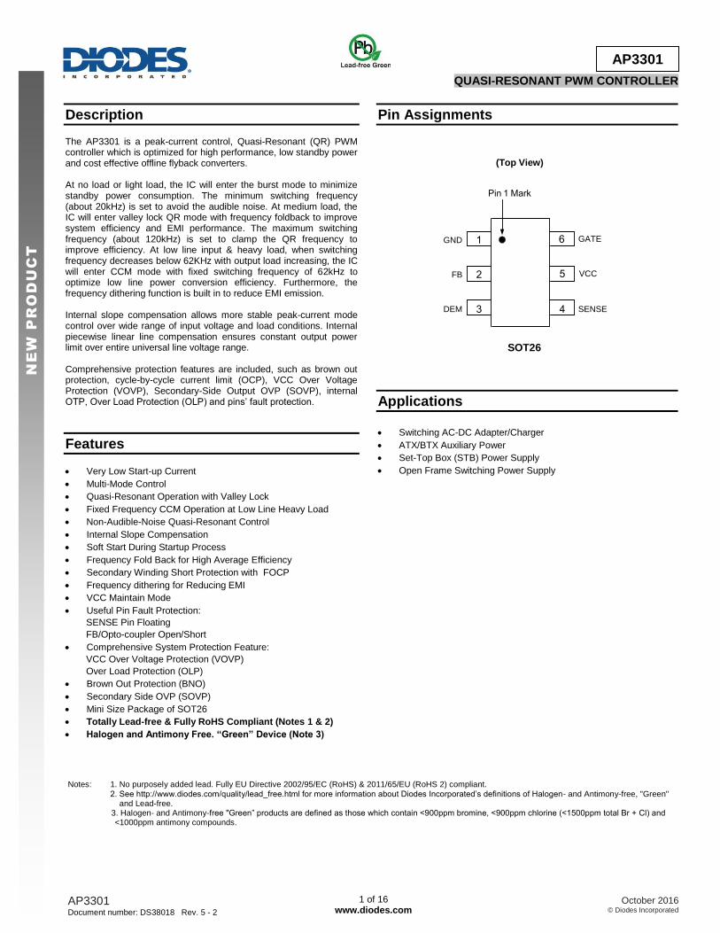
AP3301
Document number: DS38018 Rev. 5 - 2
1 of 16 www.diodes.com
October 2016 © Diodes Incorporated
AP3301
N
EW
P
RO
DU
CT
QUASI-RESONANT PWM CONTROLLER
Description The AP3301 is a peak-current control, Quasi-Resonant (QR) PWM controller which is optimized for high performance, low standby power and cost effective offline flyback converters. At no load or light load, the IC will enter the burst mode to minimize standby power consumption. The minimum switching frequency (about 20kHz) is set to avoid the audible noise. At medium load, the IC will enter valley lock QR mode with frequency foldback to improve system efficiency and EMI performance. The maximum switching frequency (about 120kHz) is set to clamp the QR frequency to improve efficiency. At low line input & heavy load, when switching frequency decreases below 62KHz with output load increasing, the IC will enter CCM mode with fixed switching frequency of 62kHz to optimize low line power conversion efficiency. Furthermore, the frequency dithering function is built in to reduce EMI emission. Internal slope compensation allows more stable peak-current mode control over wide range of input voltage and load conditions. Internal piecewise linear line compensation ensures constant output power limit over entire universal line voltage range. Comprehensive protection features are included, such as brown out protection, cycle-by-cycle current limit (OCP), VCC Over Voltage Protection (VOVP), Secondary-Side Output OVP (SOVP), internal OTP, Over Load Protection (OLP) and pins’ fault protection.
Features
Very Low Start-up Current
Multi-Mode Control
Quasi-Resonant Operation with Valley Lock
Fixed Frequency CCM Operation at Low Line Heavy Load
Non-Audible-Noise Quasi-Resonant Control
Internal Slope Compensation
Soft Start During Startup Process
Frequency Fold Back for High Average Efficiency
Secondary Winding Short Protection with FOCP
Frequency dithering for Reducing EMI
VCC Maintain Mode
Useful Pin Fault Protection:
SENSE Pin Floating
FB/Opto-coupler Open/Short
Comprehensive System Protection Feature:
VCC Over Voltage Protection (VOVP)
Over Load Protection (OLP)
Brown Out Protection (BNO)
Secondary Side OVP (SOVP)
Mini Size Package of SOT26
Totally Lead-free & Fully RoHS Compliant (Notes 1 & 2)
Halogen and Antimony Free. “Green” Device (Note 3)
Pin Assignments
(Top View)
SOT26
Applications
Switching AC-DC Adapter/Charger
ATX/BTX Auxiliary Power
Set-Top Box (STB) Power Supply
Open Frame Switching Power Supply
Notes: 1. No purposely added lead. Fully EU Directive 2002/95/EC (RoHS) & 2011/65/EU (RoHS 2) compliant.
2. See http://www.diodes.com/quality/lead_free.html for more information about Diodes Incorporated’s definitions of Halogen- and Antimony-free, "Green" and Lead-free. 3. Halogen- and Antimony-free "Green” products are defined as those which contain <900ppm bromine, <900ppm chlorine (<1500ppm total Br + Cl) and <1000ppm antimony compounds.
1
2
3 4
5
Pin 1 Mark
6GND
FB
DEM
GATE
VCC
SENSE
AP3301
Document number: DS38018 Rev. 5 - 2
2 of 16 www.diodes.com
October 2016 © Diodes Incorporated
AP3301
N
EW
P
RO
DU
CT
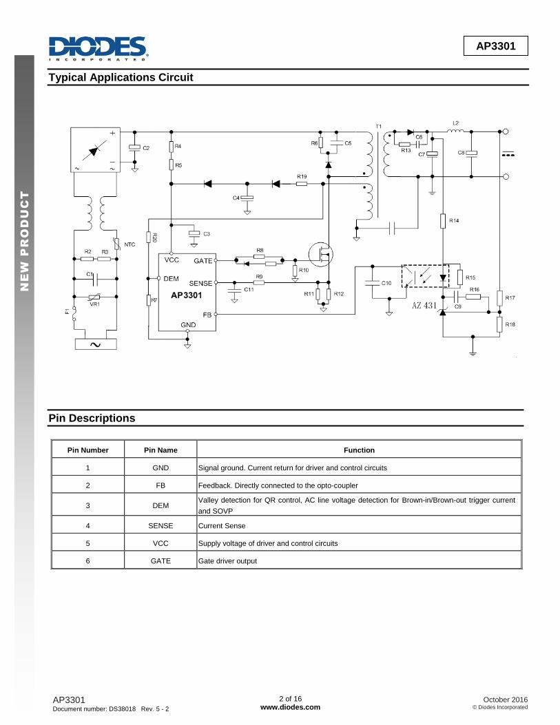
Typical Applications Circuit
Pin Descriptions
Pin Number Pin Name Function
1 GND Signal ground. Current return for driver and control circuits
2 FB Feedback. Directly connected to the opto-coupler
3 DEM Valley detection for QR control, AC line voltage detection for Brown-in/Brown-out trigger current
and SOVP
4 SENSE Current Sense
5 VCC Supply voltage of driver and control circuits
6 GATE Gate driver output
AP3301
Document number: DS38018 Rev. 5 - 2
3 of 16 www.diodes.com
October 2016 © Diodes Incorporated
AP3301
N
EW
P
RO
DU
CT
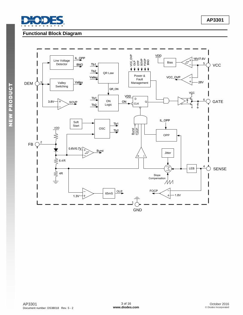
Functional Block Diagram
FB
SENSE
6.4R
4R
DEM
GATE
GND
VCC
VDD
Slope
Compensation
2
Line Voltage
Detector
Valley
Switching
SOVP3.8V
IL_OPP
BNO
Valley
OSC
Tb1
Tb2
Burst0.6V/0.7V
1.3V65mS
OLP
Soft
Start
LEB
Jitter
D
CLKQ
OPP
QR Law
Tb1
Tb2
Valley
QR_ON
ON
Logic
IL_OPP
ON
Power &
Fault
Management
VCC
16V/7.6V
Bias
VDD
28V
VCC_OVP
VC
C_O
VP
OL
P
OT
P
SO
VP
1.8V
FOCP
FO
CP
BN
O
Tb1
Tb2
Bu
rst
FO
CP
VDD
1
2
3
4
5
6
AP3301
Document number: DS38018 Rev. 5 - 2
4 of 16 www.diodes.com
October 2016 © Diodes Incorporated
AP3301
N
EW
P
RO
DU
CT
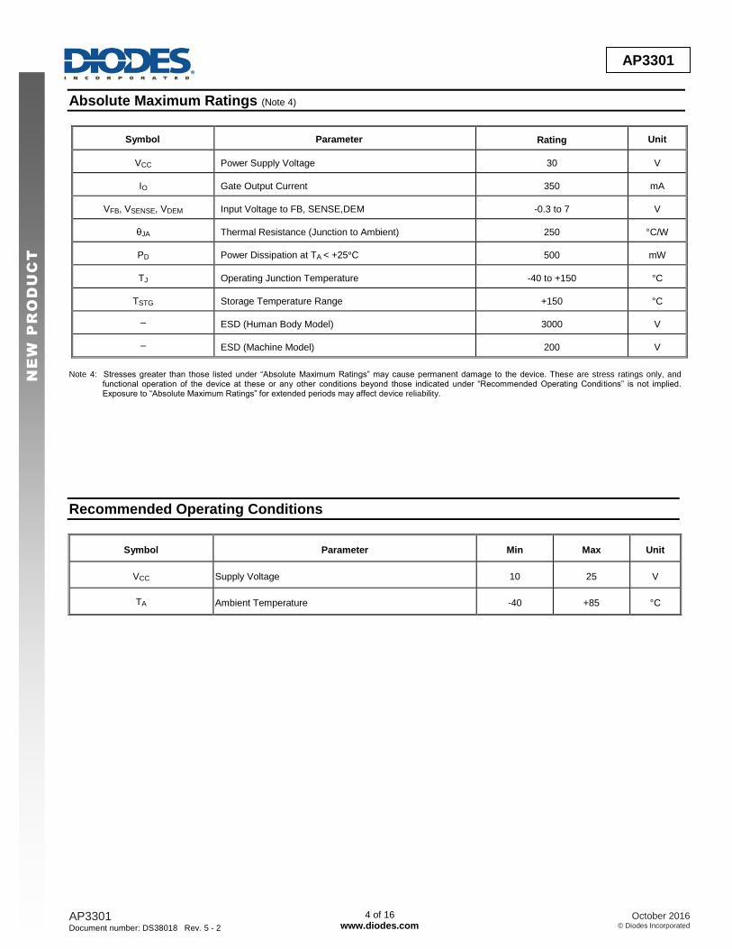
Absolute Maximum Ratings (Note 4)
Symbol Parameter Rating Unit
VCC Power Supply Voltage 30 V
IO Gate Output Current 350 mA
VFB, VSENSE, VDEM Input Voltage to FB, SENSE,DEM -0.3 to 7 V
θJA Thermal Resistance (Junction to Ambient) 250 °C/W
PD Power Dissipation at TA < +25°C 500 mW
TJ Operating Junction Temperature -40 to +150 °C
TSTG Storage Temperature Range +150 °C
– ESD (Human Body Model) 3000 V
– ESD (Machine Model) 200 V
Note 4: Stresses greater than those listed under “Absolute Maximum Ratings” may cause permanent damage to the device. These are stress ratings only, and
functional operation of the device at these or any other conditions beyond those indicated under “Recommended Operating Conditions” is not implied. Exposure to “Absolute Maximum Ratings” for extended periods may affect device reliability.
Recommended Operating Conditions
Symbol Parameter Min Max Unit
VCC Supply Voltage 10 25 V
TA Ambient Temperature -40 +85 °C
AP3301
Document number: DS38018 Rev. 5 - 2
5 of 16 www.diodes.com
October 2016 © Diodes Incorporated
AP3301
N
EW
P
RO
DU
CT
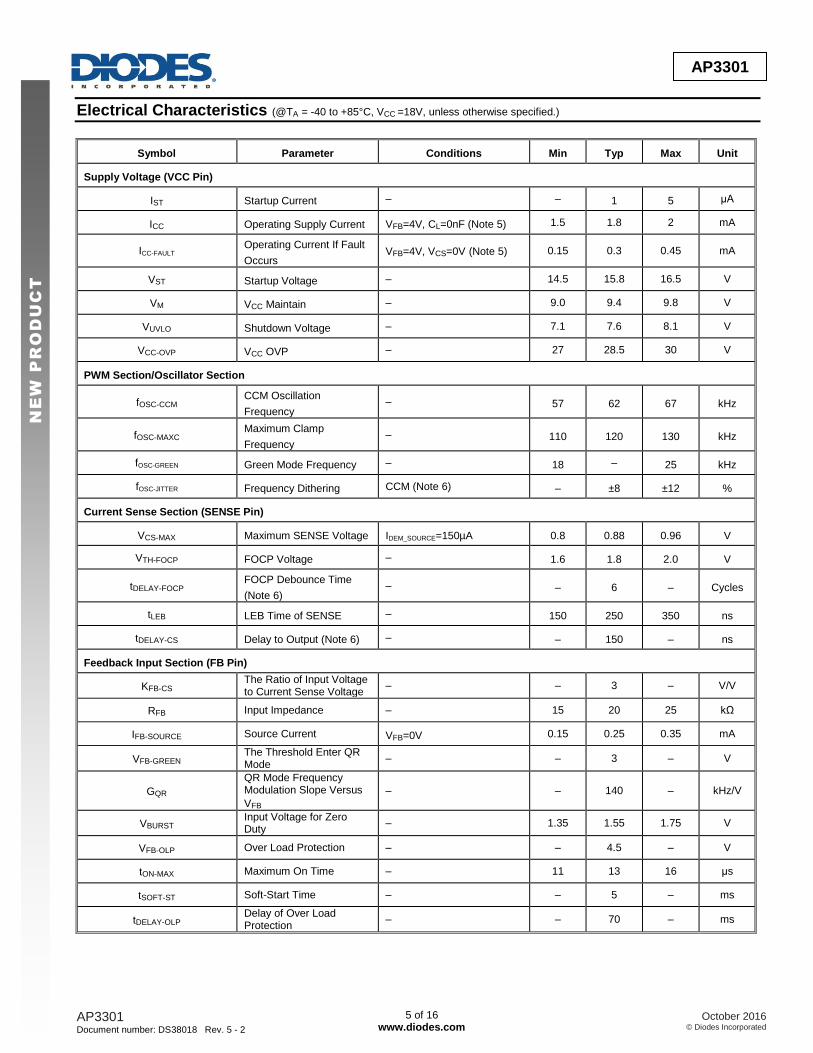
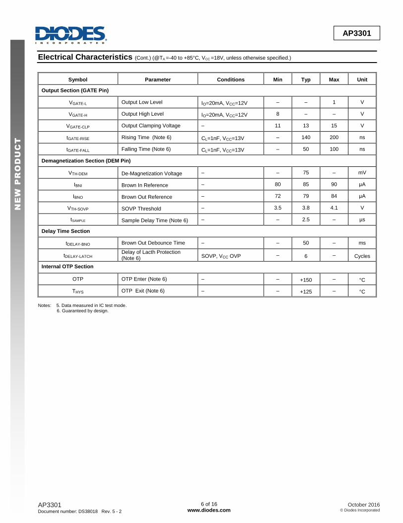
Electrical Characteristics (@TA = -40 to +85°C, VCC =18V, unless otherwise specified.)
Symbol Parameter Conditions Min Typ Max Unit
Supply Voltage (VCC Pin)
IST Startup Current – – 1 5 μA
ICC Operating Supply Current VFB=4V, CL=0nF (Note 5) 1.5 1.8 2 mA
ICC-FAULT Operating Current If Fault
Occurs VFB=4V, VCS=0V (Note 5) 0.15 0.3 0.45 mA
VST Startup Voltage – 14.5 15.8 16.5 V
VM VCC Maintain – 9.0 9.4 9.8 V
VUVLO Shutdown Voltage – 7.1 7.6 8.1 V
VCC-OVP VCC OVP – 27 28.5 30 V
PWM Section/Oscillator Section
fOSC-CCM CCM Oscillation
Frequency – 57 62 67 kHz
fOSC-MAXC Maximum Clamp
Frequency – 110 120 130 kHz
fOSC-GREEN Green Mode Frequency – 18 – 25 kHz
fOSC-JITTER Frequency Dithering CCM (Note 6) – ±8 ±12 %
Current Sense Section (SENSE Pin)
VCS-MAX Maximum SENSE Voltage IDEM_SOURCE=150µA 0.8 0.88 0.96 V
VTH-FOCP FOCP Voltage – 1.6 1.8 2.0 V
tDELAY-FOCP FOCP Debounce Time
(Note 6) – – 6 – Cycles
tLEB LEB Time of SENSE – 150 250 350 ns
tDELAY-CS Delay to Output (Note 6) – – 150 – ns
Feedback Input Section (FB Pin)
KFB-CS The Ratio of Input Voltage to Current Sense Voltage
– – 3 – V/V
RFB Input Impedance – 15 20 25 kΩ
IFB-SOURCE Source Current VFB=0V 0.15 0.25 0.35 mA
VFB-GREEN The Threshold Enter QR Mode
– – 3 – V
GQR QR Mode Frequency Modulation Slope Versus
VFB
– – 140 – kHz/V
VBURST Input Voltage for Zero Duty
– 1.35 1.55 1.75 V
VFB-OLP Over Load Protection – – 4.5 – V
tON-MAX Maximum On Time – 11 13 16 μs
tSOFT-ST Soft-Start Time – – 5 – ms
tDELAY-OLP Delay of Over Load Protection
– – 70 – ms
AP3301
Document number: DS38018 Rev. 5 - 2
6 of 16 www.diodes.com
October 2016 © Diodes Incorporated
AP3301
N
EW
P
RO
DU
CT
Electrical Characteristics (Cont.) (@TA =-40 to +85°C, VCC =18V, unless otherwise specified.)
Symbol Parameter Conditions Min Typ Max Unit
Output Section (GATE Pin)
VGATE-L Output Low Level IO=20mA, VCC=12V – – 1 V
VGATE-H Output High Level IO=20mA, VCC=12V 8 – – V
VGATE-CLP Output Clamping Voltage – 11 13 15 V
tGATE-RISE Rising Time (Note 6) CL=1nF, VCC=13V – 140 200 ns
tGATE-FALL Falling Time (Note 6) CL=1nF, VCC=13V – 50 100 ns
Demagnetization Section (DEM Pin)
VTH-DEM De-Magnetization Voltage – – 75 – mV
IBNI Brown In Reference – 80 85 90 μA
IBNO Brown Out Reference – 72 79 84 μA
VTH-SOVP SOVP Threshold – 3.5 3.8 4.1 V
tSAMPLE Sample Delay Time (Note 6) – – 2.5 – µs
Delay Time Section
tDELAY-BNO Brown Out Debounce Time – – 50 – ms
tDELAY-LATCH Delay of Lacth Protection (Note 6) SOVP, VCC OVP – 6 – Cycles
Internal OTP Section
OTP OTP Enter (Note 6) – – +150 – °C
THYS OTP Exit (Note 6) – – +125 – °C
Notes: 5. Data measured in IC test mode. 6. Guaranteed by design.
AP3301
Document number: DS38018 Rev. 5 - 2
7 of 16 www.diodes.com
October 2016 © Diodes Incorporated
AP3301
N
EW
P
RO
DU
CT
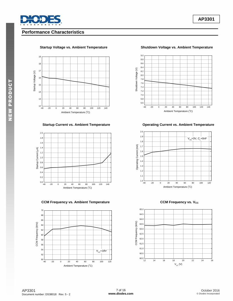
Performance Characteristics
Startup Voltage vs. Ambient Temperature Shutdown Voltage vs. Ambient Temperature
Startup Current vs. Ambient Temperature Operating Current vs. Ambient Temperature
-40 -20 0 20 40 60 80 100 120 1400.0
0.2
0.4
0.6
0.8
1.0
1.2
1.4
1.6
1.8
2.0
Sta
rtu
p C
urr
en
t (
A)
Ambient Temperature (oC)
CCM Frequency vs. Ambient Temperature CCM Frequency vs. VCC
-40 -20 0 20 40 60 80 100 1201.0
1.1
1.2
1.3
1.4
1.5
1.6
1.7
1.8
1.9
2.0
Op
era
tin
g C
urr
en
t (m
A)
Ambient Temperature (oC)
VFB
=3V, CL=0nF
-40 -20 0 20 40 60 80 100 120 14012
13
14
15
16
17
18
19
Sta
rtu
p V
olta
ge
(V
)
Ambient Temperature (oC)
-40 -20 0 20 40 60 80 100 120 140
6.6
6.8
7.0
7.2
7.4
7.6
7.8
8.0
8.2
8.4
8.6
8.8
9.0
Sh
utd
ow
n V
olta
ge
(V
)
Ambient Temperature (oC)
-40 -20 0 20 40 60 80 100 12050
52
54
56
58
60
62
64
66
68
70
CC
M F
req
ue
ncy (
kH
z)
Ambient Temperature (oC)
VCC
=18V
12 14 16 18 20 22 24 2660.0
60.5
61.0
61.5
62.0
62.5
63.0
63.5
64.0
64.5
65.0
CC
M F
req
ue
ncy (
kH
z)
VCC
(V)
AP3301
Document number: DS38018 Rev. 5 - 2
8 of 16 www.diodes.com
October 2016 © Diodes Incorporated
AP3301
N
EW
P
RO
DU
CT
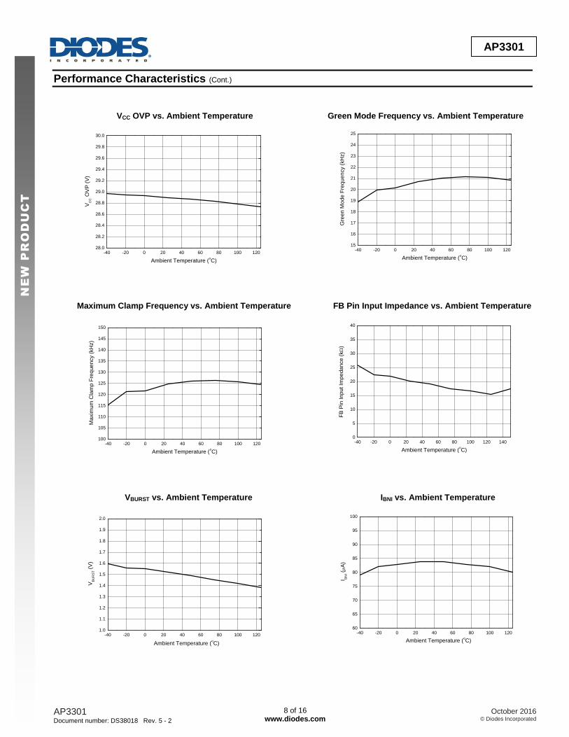
Performance Characteristics (Cont.)
VCC OVP vs. Ambient Temperature Green Mode Frequency vs. Ambient Temperature
Maximum Clamp Frequency vs. Ambient Temperature FB Pin Input Impedance vs. Ambient Temperature
VBURST vs. Ambient Temperature IBNI vs. Ambient Temperature
-40 -20 0 20 40 60 80 100 12028.0
28.2
28.4
28.6
28.8
29.0
29.2
29.4
29.6
29.8
30.0
VC
C O
VP
(V
)
Ambient Temperature (oC)
-40 -20 0 20 40 60 80 100 12015
16
17
18
19
20
21
22
23
24
25
Gre
en
Mo
de
Fre
qu
en
cy (
kH
z)
Ambient Temperature (oC)
-40 -20 0 20 40 60 80 100 120100
105
110
115
120
125
130
135
140
145
150
Ma
xim
um
Cla
mp
Fre
qu
en
cy (
kH
z)
Ambient Temperature (oC)
-40 -20 0 20 40 60 80 100 1201.0
1.1
1.2
1.3
1.4
1.5
1.6
1.7
1.8
1.9
2.0
VB
UR
ST (
V)
Ambient Temperature (oC)
-40 -20 0 20 40 60 80 100 12060
65
70
75
80
85
90
95
100
I BN
I (A
)
Ambient Temperature (oC)
-40 -20 0 20 40 60 80 100 120 1400
5
10
15
20
25
30
35
40
FB
Pin
In
pu
t Im
pe
da
nce
(k
)
Ambient Temperature (oC)
AP3301
Document number: DS38018 Rev. 5 - 2
9 of 16 www.diodes.com
October 2016 © Diodes Incorporated
AP3301
N
EW
P
RO
DU
CT
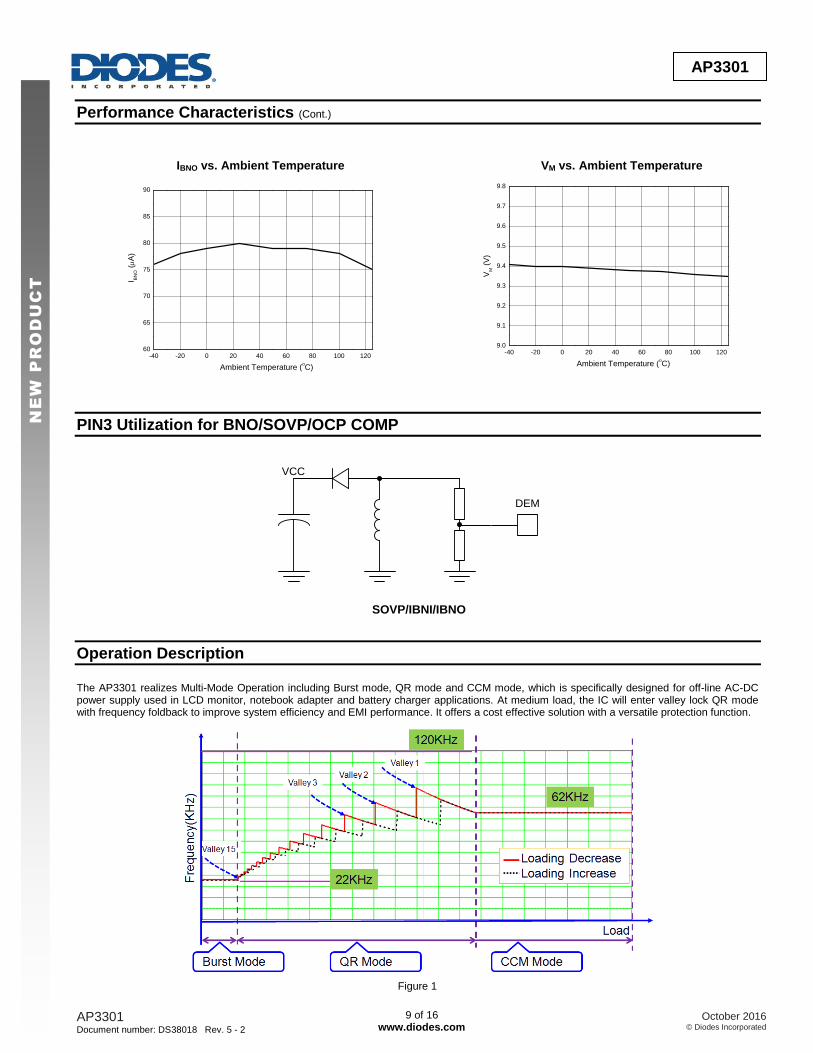
Performance Characteristics (Cont.)
IBNO vs. Ambient Temperature VM vs. Ambient Temperature
PIN3 Utilization for BNO/SOVP/OCP COMP
DEM
VCC
SOVP/IBNI/IBNO
Operation Description
The AP3301 realizes Multi-Mode Operation including Burst mode, QR mode and CCM mode, which is specifically designed for off-line AC-DC power supply used in LCD monitor, notebook adapter and battery charger applications. At medium load, the IC will enter valley lock QR mode with frequency foldback to improve system efficiency and EMI performance. It offers a cost effective solution with a versatile protection function.
Figure 1
-40 -20 0 20 40 60 80 100 12060
65
70
75
80
85
90
I BN
O (A
)
Ambient Temperature (oC)
-40 -20 0 20 40 60 80 100 1209.0
9.1
9.2
9.3
9.4
9.5
9.6
9.7
9.8
VM (
V)
Ambient Temperature (oC)
AP3301
Document number: DS38018 Rev. 5 - 2
10 of 16 www.diodes.com
October 2016 © Diodes Incorporated
AP3301
N
EW
P
RO
DU
CT
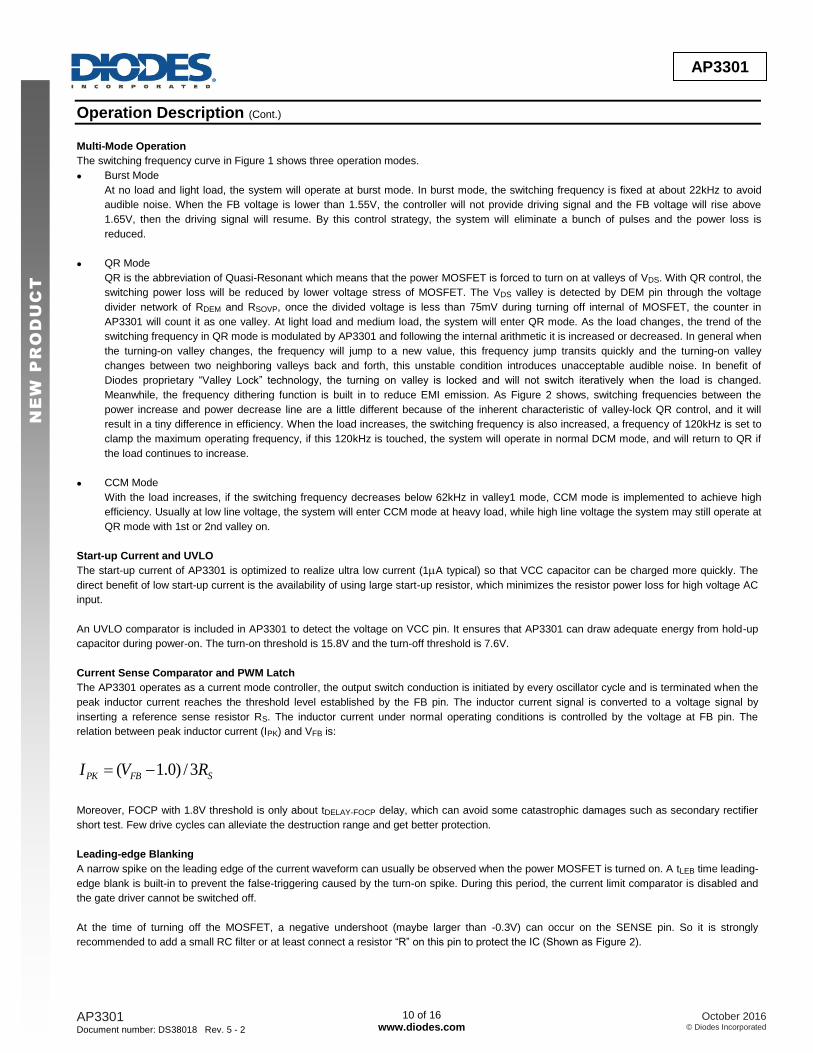
Operation Description (Cont.)
Multi-Mode Operation
The switching frequency curve in Figure 1 shows three operation modes.
Burst Mode
At no load and light load, the system will operate at burst mode. In burst mode, the switching frequency is fixed at about 22kHz to avoid
audible noise. When the FB voltage is lower than 1.55V, the controller will not provide driving signal and the FB voltage will rise above
1.65V, then the driving signal will resume. By this control strategy, the system will eliminate a bunch of pulses and the power loss is
reduced.
QR Mode
QR is the abbreviation of Quasi-Resonant which means that the power MOSFET is forced to turn on at valleys of VDS. With QR control, the
switching power loss will be reduced by lower voltage stress of MOSFET. The VDS valley is detected by DEM pin through the voltage
divider network of RDEM and RSOVP, once the divided voltage is less than 75mV during turning off internal of MOSFET, the counter in
AP3301 will count it as one valley. At light load and medium load, the system will enter QR mode. As the load changes, the trend of the
switching frequency in QR mode is modulated by AP3301 and following the internal arithmetic it is increased or decreased. In general when
the turning-on valley changes, the frequency will jump to a new value, this frequency jump transits quickly and the turning-on valley
changes between two neighboring valleys back and forth, this unstable condition introduces unacceptable audible noise. In benefit of
Diodes proprietary “Valley Lock” technology, the turning on valley is locked and will not switch iteratively when the load is changed.
Meanwhile, the frequency dithering function is built in to reduce EMI emission. As Figure 2 shows, switching frequencies between the
power increase and power decrease line are a little different because of the inherent characteristic of valley-lock QR control, and it will
result in a tiny difference in efficiency. When the load increases, the switching frequency is also increased, a frequency of 120kHz is set to
clamp the maximum operating frequency, if this 120kHz is touched, the system will operate in normal DCM mode, and will return to QR if
the load continues to increase.
CCM Mode
With the load increases, if the switching frequency decreases below 62kHz in valley1 mode, CCM mode is implemented to achieve high
efficiency. Usually at low line voltage, the system will enter CCM mode at heavy load, while high line voltage the system may still operate at
QR mode with 1st or 2nd valley on.
Start-up Current and UVLO
The start-up current of AP3301 is optimized to realize ultra low current (1A typical) so that VCC capacitor can be charged more quickly. The
direct benefit of low start-up current is the availability of using large start-up resistor, which minimizes the resistor power loss for high voltage AC
input.
An UVLO comparator is included in AP3301 to detect the voltage on VCC pin. It ensures that AP3301 can draw adequate energy from hold-up
capacitor during power-on. The turn-on threshold is 15.8V and the turn-off threshold is 7.6V.
Current Sense Comparator and PWM Latch
The AP3301 operates as a current mode controller, the output switch conduction is initiated by every oscillator cycle and is terminated when the
peak inductor current reaches the threshold level established by the FB pin. The inductor current signal is converted to a voltage signal by
inserting a reference sense resistor RS. The inductor current under normal operating conditions is controlled by the voltage at FB pin. The
relation between peak inductor current (IPK) and VFB is:
SFBPK RVI 3/)0.1(
Moreover, FOCP with 1.8V threshold is only about tDELAY-FOCP delay, which can avoid some catastrophic damages such as secondary rectifier
short test. Few drive cycles can alleviate the destruction range and get better protection.
Leading-edge Blanking
A narrow spike on the leading edge of the current waveform can usually be observed when the power MOSFET is turned on. A tLEB time leading-
edge blank is built-in to prevent the false-triggering caused by the turn-on spike. During this period, the current limit comparator is disabled and
the gate driver cannot be switched off.
At the time of turning off the MOSFET, a negative undershoot (maybe larger than -0.3V) can occur on the SENSE pin. So it is strongly
recommended to add a small RC filter or at least connect a resistor “R” on this pin to protect the IC (Shown as Figure 2).
AP3301
Document number: DS38018 Rev. 5 - 2
11 of 16 www.diodes.com
October 2016 © Diodes Incorporated
AP3301
N
EW
P
RO
DU
CT
Operation Description (Cont.)
Figure 2
Built-in Slope Compensation It is well known that a continuous current mode SMPS may become unstable when the duty cycle exceeds 50%. The built-in slope compensation can improve the stability, so there is no need for design engineer to spend much time on that.
FB Pin and Short Circuit Protection
This pin is normally connected to the opto-coupler and always paralleled with a capacitor for loop compensation. When the voltage at this pin is
greater than VFB-OLP and lasts for about tDELAY-OLP, the IC will enter the protection mode. For AP3301, the system will enter hiccup mode to wait
the VCC decreasing to low UVLO level, then the IC will try to restart until the failure removed. And when this voltage is less than 1.55V, the IC will
stop the drive pulse immediately. Therefore, this feature can be used for short circuit protection, which makes the system immune from damage.
Normally, output short makes the VFB value to the maximum because the opto-coupler is cut off.
When VCC decreases to a setting threshold, the VCC maintain comparator will output some drive signal to make the system switch and provide a
proper energy to VCC pin. The VCC maintain function will cooperate with the PWM and burst mode loop which can make the output voltage
variation be within the regulation. This mode is very useful for reducing startup resistor loss and achieving a better standby performance with a
low value VCC capacitor. The VCC is not easy to touch the shutdown threshold during the startup process and step load. This will also simplify the
system design. The minimum VCC voltage is suggested to be designed a little higher than VCC maintain threshold thus can achieve the best
balance between the standby and step load performance.
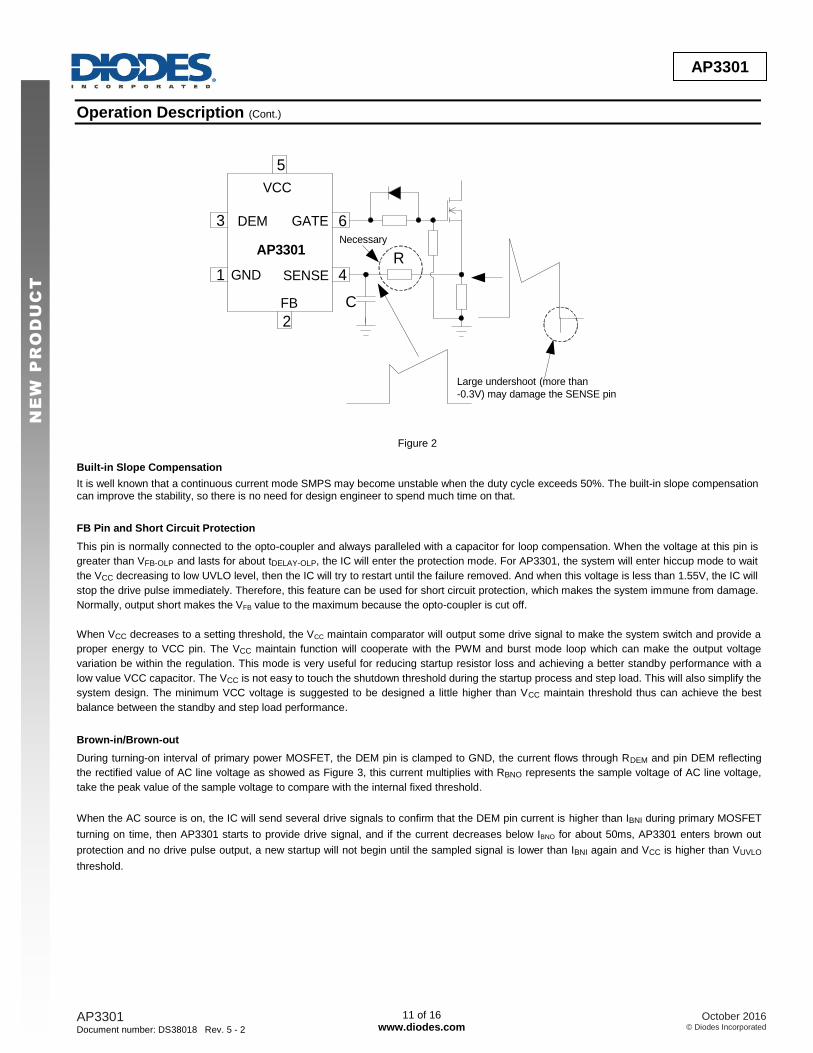
Brown-in/Brown-out
During turning-on interval of primary power MOSFET, the DEM pin is clamped to GND, the current flows through RDEM and pin DEM reflecting
the rectified value of AC line voltage as showed as Figure 3, this current multiplies with RBNO represents the sample voltage of AC line voltage,
take the peak value of the sample voltage to compare with the internal fixed threshold.
When the AC source is on, the IC will send several drive signals to confirm that the DEM pin current is higher than IBNI during primary MOSFET
turning on time, then AP3301 starts to provide drive signal, and if the current decreases below IBNO for about 50ms, AP3301 enters brown out
protection and no drive pulse output, a new startup will not begin until the sampled signal is lower than IBNI again and VCC is higher than VUVLO
threshold.
FB
SENSE
GATE
GND
DEM 6
1
3
4
AP3301
VCC
5
2
Large undershoot (more than
-0.3V) may damage the SENSE pin
R
C
Necessary
AP3301
Document number: DS38018 Rev. 5 - 2
12 of 16 www.diodes.com
October 2016 © Diodes Incorporated
AP3301
N
EW
P
RO
DU
CT
Operation Description (Cont.)
Figure 3
SOVP Protection Function
For some applications, the system requires the output over voltage protection function. The DEM pin compares the divided voltage from the VCC
winding with the inner threshold, when the voltage between RDEM and RSOVP is higher than VTH-SOVP during primary power MOSFET turning off
duration, AP3301 will trigger SOVP function and the system will enter the latch protection mode. Since the value of VCC winding’s waveform
reflects the output voltage precisely, the Secondary Output Voltage Protection (SOVP) can be achieved by this function.
Other System Protection and Pin Fault Protection
The AP3301 provides versatile system and pin fault protections. The OCP comparator realizes the cycle-by-cycle current limiting (OCP). In
universal input line voltage, the IC realizes the constant over load protection (OLP). VCC over voltage protection can be applied as the primary
OVP or opto-coupler broken protection. The AP3301 also has pin fault connection protection including floating and short connection. The floating
pin protection includes the SENSE, FB, etc. The short pin protection includes the DEM pin short protection. When these pins are floated or DEM
pin is shorted to ground, PWM switching will be disabled, thus protecting the power system.
Internal OTP Protection Function
The AP3301 integrates an internal temperature sensor. It has a trigger window of entering OTP mode at +150°C and exiting at +125°C. The
internal OTP protection mode is auto-recovery mode.
DEM 3 Line Voltage
Detector
Auxiliary
4
RDEM
RSOVP
RBNO
ROPP
OCP VREF 1
BNO VREF _ H VREF _ L
21 1 1 :
HV
Gate
RS RF CF
SENSE
Inside AP 3301
IL_O
PP
IL_B
NO
IBNI/IBNO
AP3301
Document number: DS38018 Rev. 5 - 2
13 of 16 www.diodes.com
October 2016 © Diodes Incorporated
AP3301
N
EW
P
RO
DU
CT
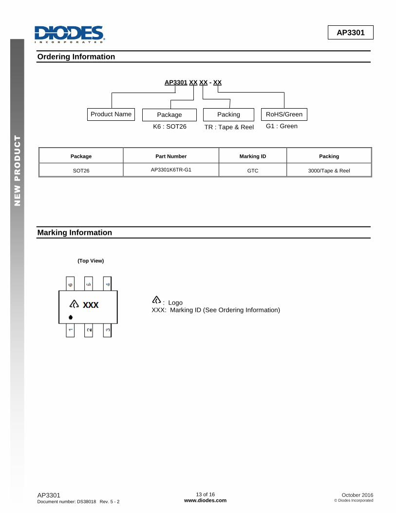
Ordering Information
AP3301 XX XX - XX
Packing
TR : Tape & Reel G1 : Green
Product Name RoHS/GreenPackage
K6 : SOT26
Package Part Number Marking ID Packing
SOT26 AP3301K6TR-G1 GTC 3000/Tape & Reel
Marking Information
(Top View)
: Logo XXX: Marking ID (See Ordering Information)
AP3301
Document number: DS38018 Rev. 5 - 2
14 of 16 www.diodes.com
October 2016 © Diodes Incorporated
AP3301
N
EW
P
RO
DU
CT
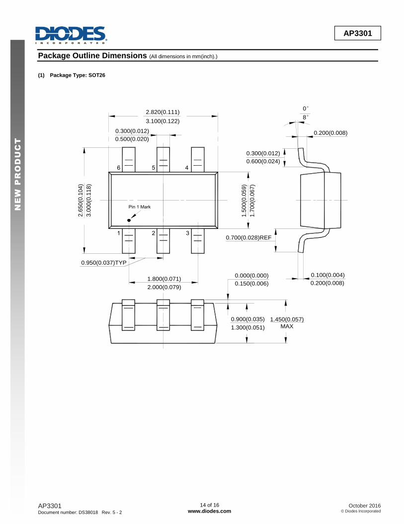
Package Outline Dimensions (All dimensions in mm(inch).)
(1) Package Type: SOT26
2.820(0.111)
3.100(0.122)
2.6
50
(0.1
04
)
3.0
00
(0.1
18
)
1.5
00
(0.0
59
)
1.7
00
(0.0
67
)
0.950(0.037)TYP
1.800(0.071)
2.000(0.079)
0.300(0.012)
0.500(0.020)
0.700(0.028)REF
0.100(0.004)
0.200(0.008)
0°
8°
0.200(0.008)
0.300(0.012)
0.600(0.024)
0.000(0.000)
0.150(0.006)
0.900(0.035)
1.300(0.051)
1.450(0.057)
MAX
1 2 3
456
Pin 1 Mark
AP3301
Document number: DS38018 Rev. 5 - 2
15 of 16 www.diodes.com
October 2016 © Diodes Incorporated
AP3301
N
EW
P
RO
DU
CT
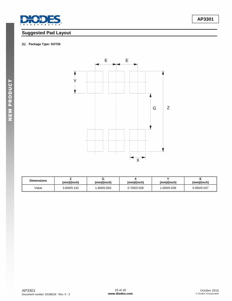
Suggested Pad Layout
(1) Package Type: SOT26
E E
G Z
Y
X
Dimensions Z
(mm)/(inch) G
(mm)/(inch) X
(mm)/(inch) Y
(mm)/(inch) E
(mm)/(inch)
Value 3.600/0.142 1.600/0.063 0.700/0.028 1.000/0.039 0.950/0.037
AP3301
Document number: DS38018 Rev. 5 - 2
16 of 16 www.diodes.com
October 2016 © Diodes Incorporated
AP3301
N
EW
P
RO
DU
CT
IMPORTANT NOTICE DIODES INCORPORATED MAKES NO WARRANTY OF ANY KIND, EXPRESS OR IMPLIED, WITH REGARDS TO THIS DOCUMENT, INCLUDING, BUT NOT LIMITED TO, THE IMPLIED WARRANTIES OF MERCHANTABILITY AND FITNESS FOR A PARTICULAR PURPOSE (AND THEIR EQUIVALENTS UNDER THE LAWS OF ANY JURISDICTION). Diodes Incorporated and its subsidiaries reserve the right to make modifications, enhancements, improvements, corrections or other changes without further notice to this document and any product described herein. Diodes Incorporated does not assume any liability arising out of the application or use of this document or any product described herein; neither does Diodes Incorporated convey any license under its patent or trademark rights, nor the rights of others. Any Customer or user of this document or products described herein in such applications shall assume all risks of such use and will agree to hold Diodes Incorporated and all the companies whose products are represented on Diodes Incorporated website, harmless against all damages. Diodes Incorporated does not warrant or accept any liability whatsoever in respect of any products purchased through unauthorized sales channel. Should Customers purchase or use Diodes Incorporated products for any unintended or unauthorized application, Customers shall indemnify and hold Diodes Incorporated and its representatives harmless against all claims, damages, expenses, and attorney fees arising out of, directly or indirectly, any claim of personal injury or death associated with such unintended or unauthorized application. Products described herein may be covered by one or more United States, international or foreign patents pending. Product names and markings noted herein may also be covered by one or more United States, international or foreign trademarks. This document is written in English but may be translated into multiple languages for reference. Only the English version of this document is the final and determinative format released by Diodes Incorporated.
LIFE SUPPORT Diodes Incorporated products are specifically not authorized for use as critical components in life support devices or systems without the express written approval of the Chief Executive Officer of Diodes Incorporated. As used herein: A. Life support devices or systems are devices or systems which: 1. are intended to implant into the body, or
2. support or sustain life and whose failure to perform when properly used in accordance with instructions for use provided in the labeling can be reasonably expected to result in significant injury to the user.
B. A critical component is any component in a life support device or system whose failure to perform can be reasonably expected to cause the failure of the life support device or to affect its safety or effectiveness. Customers represent that they have all necessary expertise in the safety and regulatory ramifications of their life support devices or systems, and acknowledge and agree that they are solely responsible for all legal, regulatory and safety-related requirements concerning their products and any use of Diodes Incorporated products in such safety-critical, life support devices or systems, notwithstanding any devices- or systems-related information or support that may be provided by Diodes Incorporated. Further, Customers must fully indemnify Diodes Incorporated and its representatives against any damages arising out of the use of Diodes Incorporated products in such safety-critical, life support devices or systems. Copyright © 2016, Diodes Incorporated www.diodes.com