Embed Size (px)
Citation preview

Multicycle Processor Design in Verilog
John Chargo and Matt Falat
Department of Computer Engineering
Iowa State University
Ames, IA 50012
Email: [email protected], [email protected]
Keywords. multicycle processor design, central process unit, CPU, instruction
set, Verilog
Abstract. The purpose of this project is to design a multicycle central processing
unit. (CPU) The processor will be able to handle fifteen different instructions, including
R-type, I-type, and J type. This exercise is done to enhance our understanding of
processor design, instruction sets, and Verilog code.
Purpose of the Machine
This machine is designed to be able execute a variety of instructions in a
multicycle implementation. The multicycle implementation breaks instructions down
into multiple steps. Each step is designed to take one clock cycle. It allows each
functional block to be used more then once per instruction if they are used on different
clock cycles. This implementation has several key advantages over a single cycle
implementation. First, it can share modules, allowing the use of fewer hardware
components. Instead of multiple arithmetic logic units (ALU’s) the multicycle
implementation uses only one. Only one memory is used for the data and the instructions
also. Breaking complex instructions into steps also allows us to significantly increase the
clock cycle because we no longer have to base the clock on the instruction that takes the
longest to execute. The multicycle implementation also uses several registers to
temporarily hold the output of the previous clock cycle. These include an Instruction
register, Memory data register, ALUOut register, etc.
The multicycle machine breaks simple instructions down into a series of steps.
These steps typically are the:
1. Instruction fetch step
2. Instruction decode and Register fetch step
3. Execution, memory address computation, or branch completion step
4. Memory access or R-type instruction completion step
5. Memory read completion step
During the instruction fetch step the multicycle processor fetches instructions from the
memory and computes the address of the next instruction, by incrementing the program
counter (PC).
During the second step, the Instruction decode and register fetch step, we decode
the instruction to figure out what type it is: memory access, R-type, I-type, branch. The
format of these individual instructions will be discussed later.
The third step, the Execution, memory address computation, or branch completion
step functions in different ways depending on what type of instruction the processor is
executing. For a memory access instruction the ALU computes the memory address. An
R-type instruction uses this third step to perform the actual arithmetic. This third step is
the last step for branch and jump instructions. It is the step where the next PC address is
computed and stored.
The fourth step only takes place in load word, store word, R-type, and I-type
instructions. This step is when the load and store word instructions access the memory
and use an arithmetic-logical instruction to write its result. Values are either loaded from
memory and stored into the memory data register, or loaded from a register and stored
back into the memory. This fourth step is the last step for R-type and I-type instructions.
For R and I type instructions this is the step where the result from the ALU computation
is stored back into the destination register.
Only load instructions need the fifth step to finish up. This is the memory read
completion step. In a load instruction the value of the memory data register is stored
back into the register file.
These different steps are all controlled and orchestrated by the “brain” of the
multicycle cpu. This “brain” is the controller. The controller is a finite state machine
that works with the Opcode to walk the rest of the components through all the different
steps, or states. The controller controls when each register is allowed to write and
controls which operation the ALU is performing.
Instruction Set
The multicycle CPU can handle a total of 15 instructions. Nine of these were also
available on the single-cycle CPU implementation. Of these, there are five R-type
instructions: add, subtract, and, or, and set less than. There are three I-Type instructions:
load word, store word, and branch on equal. The jump instruction is also supported. Six
additional instructions were added to our multicycle design. These are: nor, xor, or
immediate, and immediate, add immediate, and store less than immediate. Nor and xor
were added as R-type instructions. The additional R-type instructions were implemented
by including by augmenting the ALU. They have the same op-code as other R-type
instructions, but the function code dictates the operation that is being performed. The
four additional I-Type instructions were implemented by wiring the opcode to the control
module. This is necessary because there is no function code in the instruction. Code had
to be added to the control code to read these specific opcodes. A pair of states were also

added to the state machine to handle these immediate instructions.
Instruction Format
Design Methodology
The most appropriate way to approach any project as large as a multicycle
processor design is to break it up into simple steps. To design this project we:
1. Read project requirements.
2. Discussed what we knew, and what we needed to know.
3. Decide on the implementation we wanted to work with.
4. Discuss the modifications of the implementation we want to implement
5. Clearly define the goals of the project.
6. Develop a timetable and schedule to work with.
7. Break the large CPU into individual component modules that can be coded
separately and assign these modules to the team.
8. Build individual modules.
9. Perform simple debugging of individual modules.
10. Integrate all these individual modules into one CPU.
11. Test the functionality of the CPU.
12. Debug, debug, and more debugging.
13. Discuss and add more features.
14. Document the project and the design process.
Our initial meeting was the most useful. As a team we decided on implementing a
multicycle processor because it looked fun, challenging, and educational. Also when
discussing what additions we wanted, the team decided that making a more robust ALU
would be advantageous to the CPU. Adding support for NOR and XOR would greatly
help the processor. Also, it was decided that support was for immediate instructions is
incredibly useful when programming in assembly languages, so those had to be added. A
modified schematic was sketched so the individual modules could be made.
The biggest challenge of coding the individual modules was figuring out how
each module needed to function: what inputs and outputs were needed, and what
triggered the changes. This challenge manifested itself all the way into the debugging
stage of the whole CPU. The majority of the time of this project was spent debugging the
code we had already written. This is understandable considering the complexity of the
design.
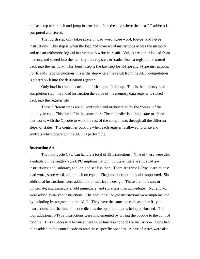
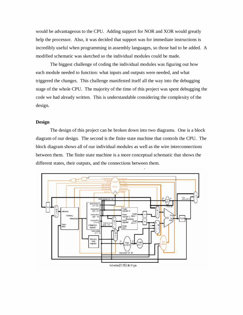
Design
The design of this project can be broken down into two diagrams. One is a block
diagram of our design. The second is the finite state machine that controls the CPU. The
block diagram shows all of our individual modules as well as the wire interconnections
between them. The finite state machine is a more conceptual schematic that shows the
different states, their outputs, and the connections between them.
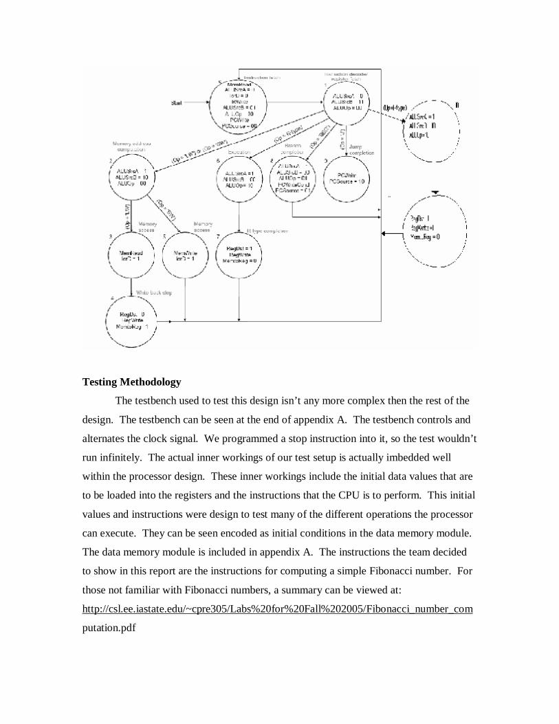
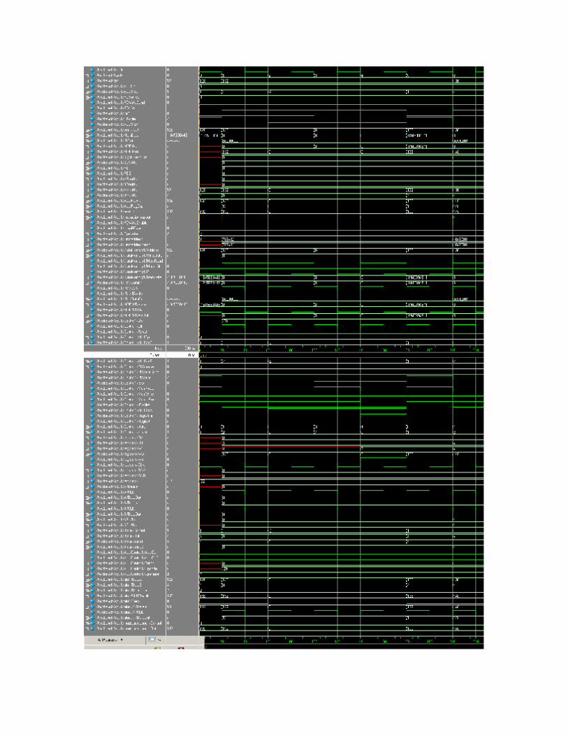
Testing Methodology
The testbench used to test this design isn’t any more complex then the rest of the
design. The testbench can be seen at the end of appendix A. The testbench controls and
alternates the clock signal. We programmed a stop instruction into it, so the test wouldn’t
run infinitely. The actual inner workings of our test setup is actually imbedded well
within the processor design. These inner workings include the initial data values that are
to be loaded into the registers and the instructions that the CPU is to perform. This initial
values and instructions were design to test many of the different operations the processor
can execute. They can be seen encoded as initial conditions in the data memory module.
The data memory module is included in appendix A. The instructions the team decided
to show in this report are the instructions for computing a simple Fibonacci number. For
those not familiar with Fibonacci numbers, a summary can be viewed at:
http://csl.ee.iastate.edu/~cpre305/Labs%20for%20Fall%202005/Fibonacci_number_com
putation.pdf

The Fibonacci number program requires that the data portion of the main memory
be initialized with 8, 1, and -1, and a series of instructions be loaded into the instruction
memory portion of the main memory.
Conclusion
The multicycle implementation of a CPU is a great improvement over a single-
cycle implementation. It allows for the use of fewer design modules and a faster clock
speed by breaking instructions into up to five different steps. These steps are controlled
by a finite state machine controller. Our design shows the implementation of a
multicycle CPU capable of handling fifteen different instructions. These instructions are
in a variety of categories: R type, I type, and j-type. Each of these categories has a
different instruction format. A multi-stepped design methodology was implemented to
break this big project into many smaller steps. This project shows the wide variety of
things to consider and components of a multicycle processor implementation.
Lessons Learned
This project enhanced the team’s knowledge of instruction sets, processor design,
instruction types, and Verilog code. The project has also given the team more practice in
engineering problem solving. The project has shown and demonstrated to the team a
design methodology that can be used for solving complex problems. There were a huge
variety of lessons learned. The team learned different things every step of the way. From
decision making and goal setting all the way up to debugging and documenting.

Appendix A: Verilog Code and Test Bench //Multicycle CPU module cpu(cycle, PC, inst, alu_out, mem_out, clock, regdst, aluop, alusrc, branch, memread, memwrite, regwrite, memtoreg, zero); // input/output input clock; output[31:0] cycle, PC, inst, alu_out, mem_out; output regdst, alusrc, branch, memread, memwrite, regwrite, memtoreg; output[1:0] aluop; output zero; // for debug reg[31:0] cycle=32'd0; always @ (posedge clock) begin cycle = cycle + 1; end // control variables wire [1:0] ALUOp, ALUSrcB, PCSource;
wire PCWriteCond, PCWrite, lorD, MemRead, MemWrite, MemtoReg, RWrite, ALUSrcA, RegWrite, RegDst;
// data path wires wire[31:0] pcmuxout, MemData, IROut, MDROut, MDRMux, SignExtendOut,
SES4Out, RD1, RD2, ARegOut, BRegOut, AMuxOut, BMuxOut, ALUResult, ALURegOut, nextpc, pcshift2out;
reg[31:0] PC=128; wire [4:0] instructionmuxout; //stuff to update PC wire PCWriteEnable; wire tempPCvar; //pcMux assign pcmuxout = lorD ? ALURegOut : PC; //memory DataMemory DataMemory1(clock, pcmuxout, BRegOut, MemWrite, MemRead,
MemData); //Instruction register IR IR1(IRWrite, MemData, IROut ,clock); //Memory Data Register MDR MDR1(MemData, MDROut ,clock);

//Controller controller Control1(clock, Reset, IROut[31:26], PCWriteCond, PCWrite, lorD,
MemRead, MemWrite, MemtoReg, IRWrite, PCSource, ALUOp, ALUSrcB, ALUSrcA, RegWrite, RegDst);
//instruction decoding assign instructionmuxout = RegDst ? IROut[15:11] : IROut[20:16]; assign MDRMux = MemtoReg ? MDROut : ALURegOut; //Registers RegFile
registers(IROut[25:21],IROut[20:16],instructionmuxout,RegWrite,MDRMux,RD 1,RD2,clock);
ABregister A(RD1, ARegOut ,clock); ABregister B(RD2, BRegOut ,clock); // sign extend and shift 2; SignExtend SE1(IROut[15:0], SignExtendOut); assign SES4Out = SignExtendOut*4; //muxes for ALU input assign AMuxOut= ALUSrcA ? ARegOut : PC; Four2One Bmux(ALUSrcB, BRegOut, 32'd4, SignExtendOut, SES4Out, BMuxOut); //ALU controller and ALU wire [3:0] Operation; ALUControl ALUControl1(IROut[31:26] ,ALUOp[1], ALUOp[0], IROut[5:0],
Operation); MainALU alu1(AMuxOut, BMuxOut, Operation, ALUResult, zero); ALUOut aluout1(ALUResult, ALURegOut ,clock); //jump stuff wire [31:0] jumpaddress; wire [27:0] jumpaddresstemp; assign jumpaddresstemp = IROut[25:0] *4; assign jumpaddress= {PC[31:28],jumpaddresstemp[27:0]}; Four2One muxfourtwoone1(PCSource, ALUResult, ALURegOut, jumpaddress,
jumpaddress, nextpc); //updating pc assign tempPCvar=zero&PCWriteCond; assign PCWriteEnable=tempPCvar|PCWrite; always@ (posedge clock) begin if(PCWriteEnable==1'b1)begin PC <= nextpc; end end endmodule

// Register File module module ABregister(DataIn, DataOut ,CLK);
input [31:0] DataIn; input CLK; output [31:0] DataOut; reg [31:0] DataOut; always @(posedge CLK) begin assign DataOut = DataIn; end endmodule // Register File module module ALUOut(DataIn, DataOut ,CLK); input [31:0] DataIn; input CLK; output [31:0] DataOut; reg [31:0] DataOut; always @(posedge CLK) begin assign DataOut = DataIn; end endmodule

// ALU Control Module, multicycle CPU module ALUControl(Opcode, ALUOp1, ALUOp0, Funct, Operation); input ALUOp1, ALUOp0; input [5:0] Funct, Opcode; output [3:0] Operation; reg [3:0] Operation; always @ (ALUOp1, ALUOp0, Funct) begin if((ALUOp1==1'b0)&(ALUOp0==1'b0)) begin Operation <= 3'b010; end if(ALUOp0==1'b1) begin Operation <= 4'b0110; end
if((ALUOp1==1'b1)&(Funct[0]==1'b0)&(Funct[1]==1'b0)&(Funct[2]==1'b0)&(
Funct[3]==1'b0)) begin Operation <= 4'b0010; end
if((ALUOp1==1'b1)&(Funct[0]==1'b0)&(Funct[1]==1'b1)&(Funct[2]==1'b0)&(
Funct[3]==1'b0)) begin Operation <= 4'b0110; end
if((ALUOp1==1'b1)&(Funct[0]==1'b0)&(Funct[1]==1'b0)&(Funct[2]==1'b1)&(
Funct[3]==1'b0)) begin Operation <= 4'b0000; end
if((ALUOp1==1'b1)&(Funct[0]==1'b1)&(Funct[1]==1'b0)&(Funct[2]==1'b1)&(
Funct[3]==1'b0)) begin Operation <= 4'b0001; end
if((ALUOp1==1'b1)&(Funct[0]==1'b0)&(Funct[1]==1'b1)&(Funct[2]==1'b0)&(
Funct[3]==1'b1)) begin Operation <= 4'b0111; end
if((ALUOp1==1'b1)&(Funct[0]==1'b1)&(Funct[1]==1'b1)&(Funct[2]==1'b1)&(
Funct[3]==1'b0)) begin Operation <= 4'b1100; end

if((ALUOp1==1'b1)&(Funct[0]==1'b0)&(Funct[1]==1'b1)&(Funct[2]==1'b1)&(
Funct[3]==1'b0)) begin Operation <= 4'b0011; end if(Opcode==6'b001000) begin //for add immediate Operation <= 4'b0010; end if(Opcode==6'b001101) begin //for or immediate Operation <= 4'b0001; end if(Opcode==6'b001100) begin // for andi Operation <= 4'b0000; end if(Opcode==6'b001010) begin // for slti Operation <= 4'b0111; end end endmodule

// Main ALU Module module MainALU(DataA, DataB, Operation, ALUResult, Zero); input [31:0] DataA, DataB; input [3:0] Operation; output [31:0] ALUResult; output Zero; reg [31:0] ALUResult; reg Zero; always @ (Operation, DataA, DataB) begin if(Operation== 4'b0010) begin ALUResult <= DataA+DataB; end if(Operation== 4'b0110) begin ALUResult <= DataA-DataB; end if(Operation== 4'b0000) begin ALUResult <= DataA&DataB; end if(Operation== 4'b0001) begin ALUResult <= DataA|DataB; end if(Operation== 4'b0111) begin if(DataB>=DataA) ALUResult <= 0; if(DataB<DataA) ALUResult <= 1; end if(Operation== 4'b1100) begin ALUResult <= ~(DataA|DataB); end if(Operation== 4'b0011) begin ALUResult <= DataA^DataB; end if(DataA==DataB) begin Zero<=1'b1; end if(~(DataA == DataB)) begin Zero<=1'b0; end
end endmodule

module controller (Clk, Reset, Op, PCWriteCond, PCWrite, lorD, MemRead, MemWrite, MemtoReg, IRWrite, PCSource, ALUOp, ALUSrcB, ALUSrcA, RegWrite, RegDst);
input [5:0] Op; input Clk, Reset; output [1:0] ALUOp, ALUSrcB, PCSource; output PCWriteCond, PCWrite, lorD, MemRead, MemWrite, MemtoReg, IRWrite,
ALUSrcA, RegWrite, RegDst; reg [1:0] ALUOp, ALUSrcB, PCSource; reg PCWriteCond, PCWrite, lorD, MemRead, MemWrite, MemtoReg, IRWrite,
ALUSrcA, RegWrite, RegDst; reg [4:0] state =0, nextstate; parameter S0=0; parameter S1=1; parameter S2=2; parameter S3=3; parameter S4=4; parameter S5=5; parameter S6=6; parameter S7=7; parameter S8=8; parameter S9=9; parameter S10=10; parameter S11=11; always@(posedge Clk) begin state=nextstate; end always @(state, Op) begin case(state) S0: begin MemRead=1'b1; ALUSrcA=1'b0; lorD= 1'b0; IRWrite=1'b1; ALUSrcB=2'b01; ALUOp= 2'b00; PCWrite=1'b1; PCSource=2'b00; nextstate=S1; RegWrite = 1'b0; MemWrite=1'b0; PCWriteCond= 1'b0; MemtoReg=1'b0; end S1: begin MemRead=1'b0;

IRWrite=1'b0; ALUSrcA=1'b0; ALUSrcB=2'b11; PCWrite=1'b0; ALUOp= 2'b00; if(Op==6'b100011) begin //if op code is lw or sw nextstate=S2; end if(Op==6'b101011) begin //if op code is lw or sw nextstate=S2; end if(Op==6'b000000) begin // if R type instruction nextstate=S6; end if(Op==6'b000100) begin //if beq instruction nextstate=S8; end if(Op==6'b000010) begin //if jump instruction nextstate=S9; end
if((Op==6'b001100)|(Op==6'b001101)|(Op==6'b001110)|(Op==6'b0011 11)) begin //if I type
nextstate=S10; end end S2: begin ALUSrcA = 1'b1; ALUSrcB= 2'b10; ALUOp = 2'b00; if(Op==6'b100011) begin //if lw nextstate=S3; end if(Op==6'b101011) begin // if SW instruction nextstate=S5; end end S3: begin MemRead=1'b1; lorD = 1'b1; nextstate=S4;

end S4: begin RegDst = 1'b0; RegWrite = 1'b1; MemtoReg= 1'b1; nextstate=S0; MemRead=1'b0; end S5: begin MemWrite=1'b1; lorD= 1'b1; nextstate=S0; end S6: begin ALUSrcA= 1'b1; ALUSrcB= 2'b00; ALUOp = 2'b10; nextstate = S7; end
S7: begin RegDst= 1'b1; RegWrite = 1'b1; MemtoReg = 1'b0; nextstate= S0; end S8: begin ALUSrcA= 1'b1; ALUSrcB= 2'b00; ALUOp=2'b01; PCWriteCond= 1'b1; PCSource = 2'b01; nextstate= S0; end S9: begin PCWrite= 1'b1; PCSource= 2'b10; nextstate= S0; end S10: begin

ALUSrcA= 1'b1; ALUSrcB= 2'b10; ALUOp = 2'b10; nextstate = S11; end S11: begin RegDst= 1'b1; RegWrite = 1'b1; MemtoReg = 1'b0; nextstate= S0; end endcase end endmodule // Register File module module IR(IRWrite, DataIn, DataOut ,CLK); input [31:0] DataIn; input CLK, IRWrite; output [31:0] DataOut; reg [31:0] DataOut; always @(posedge CLK) begin if(IRWrite==1'b1) begin DataOut <= DataIn; end end endmodule // Register File module module MDR(DataIn, DataOut ,CLK); input [31:0] DataIn; input CLK; output [31:0] DataOut; reg [31:0] DataOut; always @(posedge CLK) begin assign DataOut = DataIn; end endmodule

// Data Memory module module DataMemory(Clk, Address, WriteData, MemWrite, MemRead, MemData); input [31:0] Address, WriteData; input MemRead, MemWrite, Clk; output [31:0] MemData; wire [31:0] MemData; reg [31:0] RegFile [512:0]; always @ (posedge Clk) begin if(MemWrite==1'b1)begin RegFile[Address] <= WriteData; end end assign MemData = (MemRead==1'b1)? RegFile[Address] : 0; initial begin //load in data and instructions of program RegFile[0] <= 32'd8; RegFile[1] <= 32'd1; RegFile[2] <= 32'd1; RegFile[128] <= 32'h8c030000; RegFile[132] <= 32'h8c040001; RegFile[136] <= 32'h8c050002; RegFile[140] <=32'h8c010002; RegFile[144] <=32'h10600004; RegFile[148] <=32'h00852020; RegFile[152] <=32'h00852822; RegFile[156] <=32'h00611820; RegFile[160] <=32'h1000fffb; RegFile[164] <=32'hac040006; end endmodule
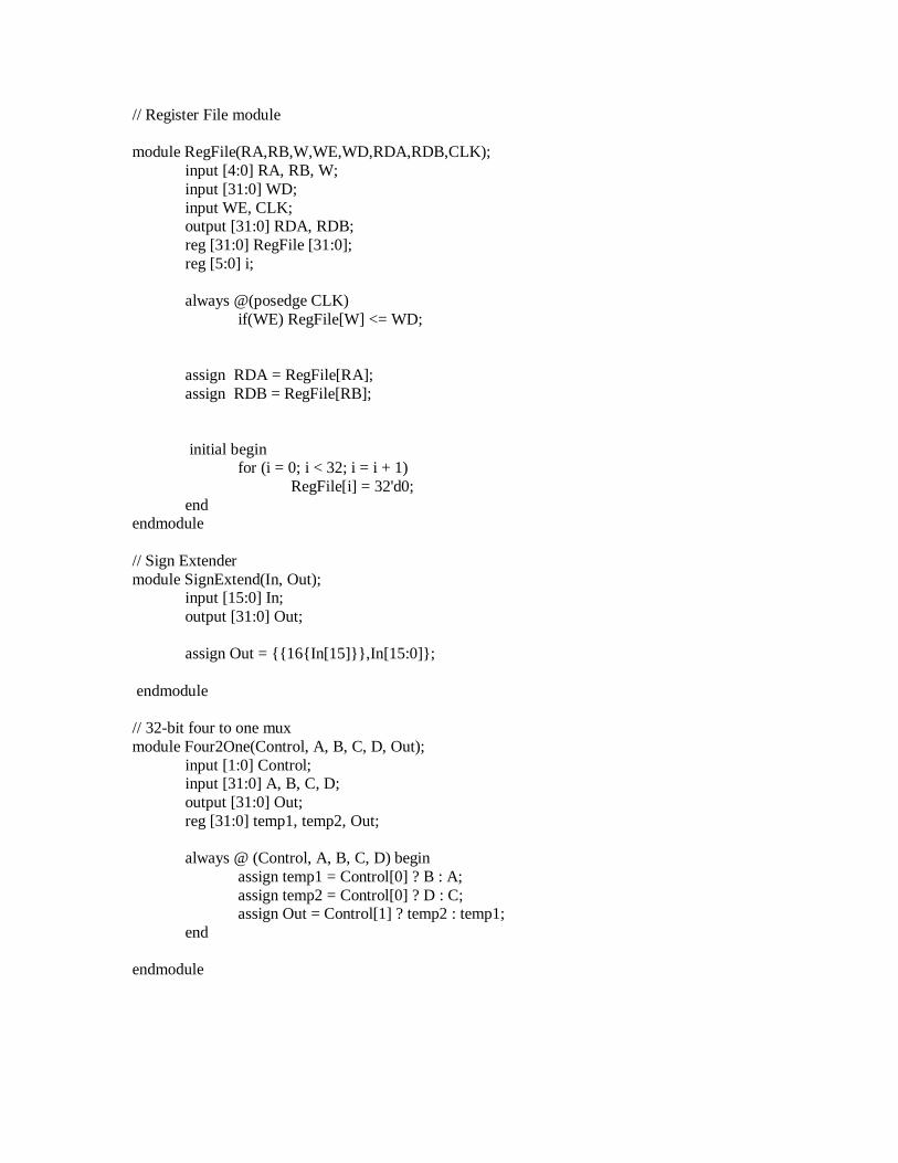
// Register File module module RegFile(RA,RB,W,WE,WD,RDA,RDB,CLK); input [4:0] RA, RB, W; input [31:0] WD; input WE, CLK; output [31:0] RDA, RDB; reg [31:0] RegFile [31:0]; reg [5:0] i; always @(posedge CLK) if(WE) RegFile[W] <= WD; assign RDA = RegFile[RA]; assign RDB = RegFile[RB]; initial begin for (i = 0; i < 32; i = i + 1) RegFile[i] = 32'd0; end endmodule // Sign Extender module SignExtend(In, Out); input [15:0] In; output [31:0] Out; assign Out = {{16{In[15]}},In[15:0]}; endmodule // 32-bit four to one mux module Four2One(Control, A, B, C, D, Out); input [1:0] Control; input [31:0] A, B, C, D; output [31:0] Out; reg [31:0] temp1, temp2, Out; always @ (Control, A, B, C, D) begin assign temp1 = Control[0] ? B : A; assign temp2 = Control[0] ? D : C; assign Out = Control[1] ? temp2 : temp1; end endmodule

//John Chargo // Multicycle CPU Testbench module testbench; reg clock=0; wire[31:0] cycle, pc, inst, alu_out, mem_out; wire regdst, alusrc, branch, memread, memwrite, regwrite, memtoreg; wire[1:0] aluop; wire zero; cpu cpu1(cycle, pc, inst, alu_out, mem_out, clock, regdst, aluop, alusrc, branch, memread, memwrite, regwrite, memtoreg, zero); always begin #20 clock<=~clock; end initial begin #2500 $stop; end
initial begin $monitor(":At Time: %d; Clk : %b; ", $time, clock); end endmodule

Appendix B: Simulation Results # Compile of AB Register.v was successful. # Compile of ALUControl.v was successful. # Compile of ALUOp.v was successful. # Compile of ALUOut Register.v was successful. # Compile of controller.v was successful. # Compile of four to one mux.v was successful. # Compile of Instruction Register.v was successful. # Compile of MainALU.v was successful. # Compile of Memory data register.v was successful. # Compile of Memory.v was successful. # Compile of Multicycle CPU.v was successful. # Compile of Registers.v was successful. # Compile of SignExtend.v was successful. # Compile of testbench.v was successful. # 14 compiles, 0 failed with no errors. vsim work.testbench # vsim work.testbench # Loading C:\Modeltech_6.0c\win32/libswiftpli.dll # Loading work.testbench # Loading work.cpu # Loading work.DataMemory # Loading work.IR # Loading work.MDR # Loading work.controller # Loading work.RegFile # Loading work.ABregister # Loading work.SignExtend # Loading work.Four2One # Loading work.ALUControl # Loading work.MainALU # Loading work.ALUOut add wave -r /* run –all


Appendix C: Mistakes often made in Verilog
Some problems arise as a result of a lack of familiarity with the Modelsim
software and verilog code. Some of the more common errors are as follows: Often when
working with a signal of multiple bits, the order of the bits is confused. Most significant
bits can be treated as least significant bits and vice versa. Also, an incorrect variable is
often used to trigger an event. A change in one input might be used to decide when to
run a piece of code when another should be used. The use of 'begin' and 'end' statements
is foreign to many of us, and misuse of these can lead to errors. Sometimes variables are
declared incorrectly. Regs and wires are confused the most often. The biggest problem
is a general lack of knowledge of the capabilities of the language. There are easier ways
to do many of the things that we do in our programs, but we are not aware of them.
Occasionally we are shown new techniques by the TA, but often these techniques would
have been useful earlier.