Embed Size (px)
DESCRIPTION
MSI 9126 manual
Citation preview

i
Version 1.0G52-S9126X1
E7205 Master-LMS-9126 (v1.X) ATX Mainboard

ii
Manual Rev: 1.0Release Date: Oct. 2002
FCC-B Radio Frequency Interference Statement
This equipment has been tested and found to comply with the limits for a classB digital device, pursuant to part 15 of the FCC rules. These limits are designedto provide reasonable protection against harmful interference when the equip-ment is operated in a commercial environment. This equipment generates, usesand can radiate radio frequency energy and, if not installed and used in accor-dance with the instruction manual, may cause harmful interference to radiocommunications. Operation of this equipment in a residential area is likely tocause harmful interference, in which case the user will be required to correctthe interference at his own expense.
Notice 1The changes or modifications not expressly approved by the party respon-sible for compliance could void the user’s authority to operate the equipment.
Notice 2Shielded interface cables and A.C. power cord, if any, must be used in order tocomply with the emission limits.
VOIR LA NOTICE D’INSTALLATION AVANT DE RACCORDER AURESEAU.
Micro-Star International MS-9126
Tested to comply with FCC Standard
For Home or Office Use

iii
Copyright Notice
The material in this document is the intellectual property of MICRO-STARINTERNATIONAL. We take every care in the preparation of this document,but no guarantee is given as to the correctness of its contents. Our productsare under continual improvement and we reserve the right to make changeswithout notice.
Trademarks
All trademarks are the properties of their respective owners.
Intel® and Pentium® are registered trademarks of Intel Corporation.PS/2 and OS®/2 are registered trademarks of International Business MachinesCorporation.Windows® 95/98/2000/NT/XP are registered trademarks of MicrosoftCorporation.Netware® is a registered trademark of Novell, Inc.Award® is a registered trademark of Phoenix Technologies Ltd.AMI® is a registered trademark of American Megatrends Inc.
Revision HistoryRevision Revision History DateV1.0 First release Oct. 2002
Technical Support
If a problem arises with your system and no solution can be obtained from theuser’s manual, please contact your place of purchase or local distributor.Alternatively, please try the following help resources for further guidance.
Visit the MSI website for FAQ, technical guide, BIOS updates, driverupdates, and other information: http://www.msi.com.tw/
Contact our technical staff at: [email protected]

iv
1. Always read the safety instructions carefully.2. Keep this User’s Manual for future reference.3. Keep this equipment away from humidity.4. Lay this equipment on a reliable flat surface before setting it up.5. The openings on the enclosure are for air convection hence protects the
equipment from overheating. DO NOT COVER THE OPENINGS.6. Make sure the voltage of the power source and adjust properly 110/220V
before connecting the equipment to the power inlet.7. Place the power cord such a way that people can not step on it. Do not
place anything over the power cord.8. Always Unplug the Power Cord before inserting any add-on card or module.9. All cautions and warnings on the equipment should be noted.10. Never pour any liquid into the opening that could damage or cause electri-
cal shock.11. If any of the following situations arises, get the equipment checked by a
service personnel:The power cord or plug is damaged.Liquid has penetrated into the equipment.The equipment has been exposed to moisture.The equipment has not work well or you can not get it work accordingto User’s Manual.The equipment has dropped and damaged.The equipment has obvious sign of breakage.
12. DO NOT LEAVE THIS EQUIPMENT IN AN ENVIRONMENTUNCONDITIONED, STORAGE TEMPERATURE ABOVE 600 C (1400F), ITMAY DAMAGE THE EQUIPMENT.
Safety Instructions
CAUTION: Danger of explosion if battery is incorrectly replaced.Replace only with the same or equivalent type recommended by themanufacturer.

v
CONTENTSFCC-B Radio Frequency Interference Statement .......................................... iiiCopyright Notice .......................................................................................... iiiRevision History ........................................................................................... iiiTechnical Support ......................................................................................... iiiSafety Instructions ....................................................................................... ivChapter 1. Getting Started ........................................................................ 1-1
Mainboard Specifications .................................................................... 1-2Mainboard Layout ............................................................................... 1-4MSI Special Features ........................................................................... 1-5
PC Alert™ III ................................................................................. 1-5Chapter 2. Hardware Setup ....................................................................... 2-1
Quick Components Guide .................................................................... 2-2Central Processing Unit: CPU .............................................................. 2-3
CPU Core Speed Derivation Procedure ......................................... 2-3CPU Installation Procedures for Socket 478 .................................. 2-4Installing the CPU Fan .................................................................. 2-5
Memory ................................................................................................ 2-7Memory Speed/CPU FSB Support Matrix ..................................... 2-7DIMM Module Combination ......................................................... 2-7Installing DDR Modules ............................................................... 2-8
Power Supply ....................................................................................... 2-9ATX 20-Pin Power Connector: JWR1 ............................................ 2-9ATX 12V Power Connector: JPW1 ................................................ 2-9
Back Panel .......................................................................................... 2-10Mouse Connector ....................................................................... 2-10Keyboard Connector ................................................................... 2-11USB Connectors .......................................................................... 2-11RJ-45 LAN Jack: Giga-bit LAN .................................................... 2-12Serial Port Connector: COM A & COM B ................................... 2-12

vi
Audio Port Connectors ............................................................... 2-13Parallel Port Connector: LPT1 ...................................................... 2-14Floppy Disk Drive Connector: FDD1........................................... 2-15
Connectors ......................................................................................... 2-15Hard Disk Connectors: IDE1 & IDE2 ........................................... 2-16Fan Power Connectors: JCFAN1, JSFAN1/2/3/4 ......................... 2-17Front Panel Connectors: JFP1 ..................................................... 2-18Front USB Connector: JUSB1 ...................................................... 2-19CD-In Connector: JCDIN1 ........................................................... 2-20Chassis Intrusion Switch Connector: JINT1 ............................... 2-20
Jumpers .............................................................................................. 2-21Clear CMOS Jumper: JCMOS1 .................................................... 2-21
Slots ................................................................................................... 2-22AGP (Accelerated Graphics Port) Pro Slot .................................. 2-22PCI (Peripheral Component Interconnect) Slots .......................... 2-22PCI Interrupt Request Routing .................................................... 2-26
Chapter 3. BIOS Setup .............................................................................. 3-1Entering Setup ...................................................................................... 3-2
Control Keys ................................................................................. 3-2Getting Help .................................................................................. 3-3
The Main Menu ................................................................................... 3-4Standard CMOS Features .................................................................... 3-6Advanced BIOS Features .................................................................... 3-8Advanced Chipset Features ............................................................... 3-12Integrated Peripherals ........................................................................ 3-16Power Management Setup ................................................................. 3-21PNP/PCI Configurations ..................................................................... 3-25PC Health Status ................................................................................ 3-27Frequency/Voltage Control ................................................................ 3-28

vii
Load Fail-Safe/Optimized Defaults ..................................................... 3-29Set Supervisor/User Password ........................................................... 3-30
Troubleshooting ........................................................................................ T-1Glossary ....................................................................................................G-1

1-1
Getting Started
Chapter 1. Gett ingStarted
Getting Started
Thank you for purchasing the E7205 Master-L (MS-9126v1.X) ATX mainboard. The E7205 Master-L is a superior compu-ter mainboard based on Intel® E7205 & ICH4 chipsets for opti-mal system efficiency. Designed to fit the advanced Intel®
Pentium® 4 processors in the 478 pin package, the motherboardprovides a cost-effective and professional solution for high per-formance PC, entry-level workstation and server markets.
1-2
MS-9126 ATX Mainboard
Mainboard Specifications
CPU Supports Intel® P4 Northwood processor in 478-pin package. Supports 1.5GHz, 1.6GHz, 1.7GHz, 1.8GHz, 1.9GH z, 2GHz and up.
Chipset Intel® E7205 chipset- Supports single processor at 533MHz.- System bus bandwidth of 4.27GB/s.- Supports AGP 8x or 4x at 0.8V (AGP 3.0) or 4x at 1.5V (3.3V not supported).- Supports 144bit wide DDR266 memory interface with the memory band
width of 4.27GB/s or 3.2 GB/s. Intel® ICH4 chipset- Hi-Speed USB (USB2.0) controller, 480Mb/sec.- 2 channel Ultra ATA 100 bus Master IDE controller.- PCI Master 2.2.- I/O APIC.- AC’97 2.2 interface.- 3 UHCI Host controllers and 1 EHCI Host controller.
Main Memory Supports dual channel (144-bit wide) DDR266 memory interface. Each chan-nel supports 2 DIMM slots.
Supports four 184-pin DDR DIMM sockets up to 4GB. Supports non-ECC (x64) or ECC (x72) DDR266 DIMMs using 128MB, 256MB,or 512MB SDRAM.
Slots One AGP Pro 50-Watt slot supports 8x/4x at 0.8V (AGP 3.0) or 4x at 1.5V (3.3Vnot supported).
Five 32-bit Master PCI bus slots (support 3.3V/5V PCI bus interface). One Mini PCI slot for PCI extender cards.
On-Board IDE An IDE controller on the ICH4 chipset provides IDE HDD/CD-ROM withPIO, Bus Master and Ultra DMA100/66/33 operation modes.
Can connect up to four IDE devices.
1-3
Getting Started
On-Board Peripherals On-Board Peripherals include:- 1 floppy port supports 2 FDDs with 360K, 720K, 1.2M, 1.44M and
2.88Mbytes- 2 serial ports (COM A + COM B)- 1 parallel port supports SPP/EPP/ECP mode- 1 RJ-45 LAN port- 4 USB 2.0 ports (Rear * 2/ Front * 2)
Onboard Audio AC’97 audio codec integrated in ICH4 south bridge. AD 1885 software audio codec. 4 audio jacks (Line-In, Line-Out, Mic-In, Headphone-Out) onboard.
LAN Intel® 82540EM Gigabit Ethernet controller.
SCSI Add-In Card (Optional) Adaptec AIC-7892B SCSI controller. Mini PCI interface.
BIOS The mainboard BIOS provides “Plug & Play” BIOS which detects the pe-ripheral devices and expansion cards of the board automatically.
The mainboard provides a Desktop Management Interface (DMI) functionwhich records your mainboard specifications.
Dimension ATX Form Factor: 12” x 9.6”.
Mounting 9 mounting holes.

1-4
MS-9126 ATX Mainboard
Mainboard Layout
E7205 Master-L (MS-9126 v1.X) ATX Mainboard
BATT+
ICH4
DIM
M 1
DIM
M 2
DIM
M 3
DIM
M 4
JUSB1
MINIPCI1
JWR
1
JFP1
JSFAN1JSFAN2
JCFAN1
JSFAN3
JSFAN4
JCMOS1
BIOS
PCI 5
PCI 4
PCI 3
PCI 2
PCI 1ID
E 1
IDE
2
Codec
Top: Parallel Port
Bottom: COM ACOM B
JAUD1
JAUD2
Top: Mouse Bottom: Keyboard
Top: LAN JackBottom: USB Ports
JCDIN1
JINT1
WinbondW83627HF-AW
JPW1
FDD
1
AGP 1
IntelE7205

1-5
Getting Started
MSI Special Features
PC Alert™ IIIThe PC AlertTM III is a utility you can find in the CD-ROM disk. The
utility is just like your PC doctor that can de-tect the following PC hardware status duringreal time operation:
monitor CPU & system temperatures monitor fan speed(s) monitor system voltage monitor chassis intrusion
If one of the items above is abnormal,the program main screen will be immediatelyshown on the screen, with the abnormal itemhighlighted in red. This will continue to beshown until user disables the warning.
MSI Reminds You...Items shown on PC Alert™ III vary depending on your system status.

2-1
Hardware Setup
Chapter 2. HardwareSetup
Hardware Setup
This chapter provides you with the information about hard-ware setup procedures. While doing the installation, be carefulin holding the components and follow the installationprocedures. For some components, if you install in the wrongorientation, the components will not work properly.
Use a grounded wrist strap before handling computercomponents. Static electricity may damage the components.

2-2
MS-9126 ATX Mainboard
Quick Components Guide
CPU, p.2-3
JCFAN1, p.2-17JPW1, p.2-9
Back PanelI/O, p.2-10
PCI1~5,p.2-22
JCMOS1,p.2-21
JFP1, p.2-18
JUSB1, p.2-19
IDE1/2,p.2-16
JWR1, p.2-9
FDD1,p.2-15
JSFAN4/3,p.2-17
DIMM1/2/3/4,p.2-7
Mini PCI,p.2-22
JCDIN1, p.2-20
JINT1, p.2-20
JSFAN2/1,p.2-17

2-3
Hardware Setup
Central Processing Unit: CPU
CPU Core Speed Derivation Procedure
If CPU Clock = 100MHzCore/Bus ratio = 14
then CPU core speed = Host Clock x Core/Bus ratio= 100MHz x 14= 1.4 GHz
MSI Reminds You...OverheatingOverheating will seriously damage the CPU and system, al-ways make sure the cooling fan can work properly to protectthe CPU from overheating.
Replacing the CPUWhile replacing the CPU, always turn off the ATX power sup-ply or unplug the power supply’s power cord from groundedoutlet first to ensure the safety of CPU.
OverclockingThis motherboard is designed to support overclocking.However, please make sure your components are able to toler-ate such abnormal setting, while doing overclocking. Any at-tempt to operate beyond product specifications is notrecommended. We do not guarantee the damages or riskscaused by inadequate operation or beyond productspecifications.
The mainboard supports Intel® P4 Northwood processor in the 478 pinpackage. The mainboard uses a CPU socket called PGA478 for easy CPUinstallation. When you are installing the CPU, make sure the CPU has aheat sink and a cooling fan attached on the top to prevent overheating. Ifyou do not find the heat sink and cooling fan, contact your dealer to purchaseand install them before turning on the computer.

2-4
MS-9126 ATX Mainboard
1. Please turn off the power andunplug the power cord beforeinstalling the CPU.
2. Pull the lever sideways awayfrom the socket. Make sure toraise the lever up to a 90-de-gree angle.
3. Look for the gold arrow. Thegold arrow should point to-wards the lever pivot. TheCPU can only fit in the cor-rect orientation.
4. If the CPU is correctlyinstalled, the pins should becompletely embedded into thesocket and can not be seen.Please note that any violationof the correct installation pro-cedures may cause permanentdamages to your mainboard.
5. Press the CPU down firmlyinto the socket and close thelever. As the CPU is likely tomove while the lever is beingclosed, always close the leverwith your fingers pressingtightly on top of the CPU tomake sure the CPU is prop-erly and completely embed-ded into the socket.
CPU Installation Procedures for Socket 478
Open Lever
90 degreeSliding Plate
Close Lever
Press downthe CPU
Gold arrow
Gold arrow
Gold arrow
Correct CPU placement
Incorrect CPU placement
X
O

2-5
Hardware Setup
Installing the CPU FanAs processor technology pushes to faster speeds and higher performance,
thermal management becomes increasingly important. To dissipate heat, youneed to attach the CPU cooling fan and heatsink on top of the CPU. Followthe instructions below to install the Heatsink/Fan:
2. Position the heatsink onto the reten-tion mechanism.
1. Locate the CPU and its retentionmechanism on the motherboard.
3. Mount the fan on top of the heatsink.Press down the fan until its four clipsget wedged in the holes of the reten-tion mechanism.
4. Press the two levers down to fastenthe fan. Each lever can be presseddown in only ONE direction.
retention mechanism
levers

2-6
MS-9126 ATX Mainboard
5. Connect the fan power cable from the mounted fan to the 3-pin fan power connectoron the board.
fan power cable
NOTES

2-7
Hardware Setup
The mainboard provides 4 slots for 184-pin DDR SDRAM DIMM(Double In-Line Memory Module) modules and supports up to 4GB memorysize. You can install PC2100/DDR266 or PC1600/DDR200 modules on theDDR DIMM slots (DIMM 1~4).
Memory
DDR DIMM Slots(DIMM 1~4)
DIMM Module CombinationThe mainboard supports dual channel (144-bit wide) DDR266/200
memory interface. Each channel supports 2 DIMM slots. Hence, users haveto install at least two DIMM modules on the slots.
Each DIMM slot supports up to a maximum size of 1GB. Users caninstall either single- or double-sided modules depending on their needs, butmemory modules must be installed on the board IN PAIRS.
Memory Speed/CPU FSB Support Matrix
DDR200 DDR266400MHz FSB Yes Yes533MHz FSB No Yes

2-8
MS-9126 ATX Mainboard
Installing DDR Modules1. The DDR DIMM has only one notch on the center of module. The mod-
ule will only fit in the right orientation.2. Insert the DIMM memory module vertically into the DIMM slot. Then
push it in until the golden finger on the memory module is deeply in-serted in the socket.
3. The plastic clip at each side of the DIMM slot will automatically close.
MSI Reminds You...You can barely see the golden finger if the module is properly inserted in the socket.
Volt Notch
MSI Reminds You...Make sure that you install memory modules of the same type anddensity on DDR DIMMs “in pairs” -- {DIMM1 & DIMM2}{DIMM3 & DIMM4}.
Memory modules can be installed in any combination as follows:
DIMM1 DIMM2 DIMM3 DIMM4 System Density128MB~1GB 128MB~1GB 256MB~2GB
128MB~1GB 128MB~1GB 256MB~2GB128MB~1GB 128MB~1GB 128MB~1GB 128MB~1GB 512MB~4GB

2-9
Hardware Setup
Power SupplyThe mainboard supports ATX power supply for the power system. Be-
fore inserting the power supply connector, always make sure that all compo-nents are installed properly to ensure that no damage will be caused.
ATX 20-Pin Power Connector: JWR1This connector allows you to connect to an ATX power supply. To
connect to the ATX power supply, make sure the plug of the power supply isinserted in the proper orientation and the pins are aligned. Then push downthe power supply firmly into the connector.
ATX 12V Power Connector: JPW1This 12V power connector is used to provide power to the CPU.
PIN SIGNAL
1 GND2 GND3 12V4 12V
JPW1 Pin DefinitionPIN SIGNAL
11 3.3V12 -12V13 GND14 PS_ON15 GND16 GND17 GND18 -5V19 5V20 5V
PIN SIGNAL
1 3.3V2 3.3V3 GND4 5V5 GND6 5V7 GND8 PW_OK9 5V_SB10 12V
JWR1 Pin Definition
JWR110
1
20
11JPW1
1
3 42

2-10
MS-9126 ATX Mainboard
The back panel provides the following connectors:
Back Panel
Mouse ConnectorThe mainboard provides a standard PS/2® mouse mini DIN connector
for attaching a PS/2® mouse. You can plug a PS/2® mouse directly into thisconnector. The connector location and pin assignments are as follows:
PIN SIGNAL DESCRIPTION
1 Mouse DATA Mouse DATA2 NC No connection3 GND Ground4 VCC +5V5 Mouse Clock Mouse clock6 NC No connection
Pin Definition
PS/2 Mouse (6-pin Female)2 1
34
56
Mouse
Keyboard USB
Parallel
COM A
LAN
Audio JacksCOM B

2-11
Hardware Setup
Keyboard ConnectorThe mainboard provides a standard PS/2® keyboard mini DIN connec-
tor for attaching a PS/2® keyboard. You can plug a PS/2® keyboard directlyinto this connector.
PIN SIGNAL DESCRIPTION
1 Keyboard DATA Keyboard DATA2 NC No connection3 GND Ground4 VCC +5V5 Keyboard Clock Keyboard clock6 NC No connection
Pin Definition
PS/2 Keyboard (6-pin Female)2 1
34
56
USB ConnectorsThe mainboard provides a UHCI (Universal Host Controller Interface)
Universal Serial Bus root for attaching USB devices such as keyboard, mouseor other USB-compatible devices. You can plug the USB device directly intothe connector.
PIN SIGNAL DESCRIPTION
1 VCC +5V2 -Data 0 Negative Data Channel 03 +Data0 Positive Data Channel 04 GND Ground5 VCC +5V6 -Data 1 Negative Data Channel 17 +Data 1 Positive Data Channel 18 GND Ground
USB Port Description
USB Ports
1 2 3 4
5 6 7 8

2-12
MS-9126 ATX Mainboard
RJ-45 LAN Jack: Giga-bit LANThe mainboard provides one standard RJ-45 jack for connection to
Local Area Network (LAN). Giga-bit LAN enables data to be transferred at1000, 100 or 10Mbps. Pin assignments vary depending on the transfer rates:10/100Mbps or 1000Mbps. Note that Pin 1/2, 3/6, 4/5, 7/8 must work in pairs.Please refer to the following for details:
RJ-45 LAN Jack
Activity Indicator
8 1
Speed Indicator
10/100 LAN Pin Definition
PIN SIGNAL DESCRIPTION
1 TDP Transmit Differential Pair
2 TDN Transmit Differential Pair
3 RDP Receive Differential Pair
4 NC Not Used
5 NC Not Used
6 RDN Receive Differential Pair
7 NC Not Used
8 NC Not Used
Giga-bit LAN Pin Definition
PIN SIGNAL DESCRIPTION
1 D0P Differential Pair 0+
2 D0N Differential Pair 0-
3 D1P Differential Pair 1+
4 D2P Differential Pair 2+
5 D2N Differential Pair 2-
6 D1N Differential Pair 1-
7 D3P Differential Pair 3+
8 D3N Differential Pair 3-

2-13
Hardware Setup
Serial Port Connector: COM A & COM BThe mainboard offers two 9-pin male DIN connectors as serial port COM
A and COM B. The ports are 16550A high speed communication ports thatsend/receive 16 bytes FIFOs. You can attach a serial mouse or other serialdevices directly to them.
9-Pin Male DIN Connectors
1 2 3 4 5
6 7 8 9
PIN SIGNAL DESCRIPTION
1 DCD Data Carry Detect2 SIN Serial In or Receive Data3 SOUT Serial Out or Transmit Data4 DTR Data Terminal Ready)5 GND Ground6 DSR Data Set Ready7 RTS Request To Send8 CTS Clear To Send9 RI Ring Indicate
Pin Definition
Audio Port ConnectorsLine-Out is a connector for speakers or headphones. Line-In is used
for external CD player, Tape player, or other audio devices. Mic-In is a con-nector for microphones. HP-Out is used to connect headphones if available.
Line-Out
Line-In Mic-In
HP-Out

2-14
MS-9126 ATX Mainboard
Parallel Port Connector: LPT1The mainboard provides a 25-pin female centronic connector as LPT.
A parallel port is a standard printer port that supports Enhanced Parallel Port(EPP) and Extended Capabilities Parallel Port (ECP) mode.
13 1
1425
PIN SIGNAL DESCRIPTION1 STROBE Strobe2 DATA0 Data03 DATA1 Data14 DATA2 Data25 DATA3 Data36 DATA4 Data47 DATA5 Data58 DATA6 Data69 DATA7 Data710 ACK# Acknowledge11 BUSY Busy12 PE Paper End13 SELECT Select14 AUTO FEED# Automatic Feed15 ERR# Error16 INIT# Initialize Printer17 SLIN# Select In18 GND Ground19 GND Ground20 GND Ground21 GND Ground22 GND Ground23 GND Ground24 GND Ground25 GND Ground
Pin Definition

2-15
Hardware Setup
The mainboard provides connectors to connect FDD, IDE HDD, frontpanel of the system case, audio ports, USB Ports, and CPU/System FANs.
Floppy Disk Drive Connector: FDD1The mainboard provides a standard floppy disk drive connector that
supports 360K, 720K, 1.2M, 1.44M and 2.88M floppy disk types.
Connectors
FDD1

2-16
MS-9126 ATX Mainboard
MSI Reminds You...If you install two hard disks on cable, you must configure thesecond drive to Slave mode by setting its jumper. Refer to thehard disk documentation supplied by hard disk vendors forjumper setting instructions.
Hard Disk Connectors: IDE1 & IDE2The mainboard has a 32-bit Enhanced PCI IDE and Ultra DMA 66/100
controller that provides PIO mode 0~4, Bus Master, and Ultra DMA 66/100function. You can connect up to four hard disk drives, CD-ROM, 120MBFloppy (reserved for future BIOS) and other devices. These connectors sup-port the provided IDE hard disk cable.
IDE1 (Primary IDE Connector)The first hard drive should always be connected to IDE1. IDE1 canconnect a Master and a Slave drive. You must configure second harddrive to Slave mode by setting the jumper accordingly.
IDE2 (Secondary IDE Connector)IDE2 can also connect a Master and a Slave drive.
IDE1IDE2
2-17
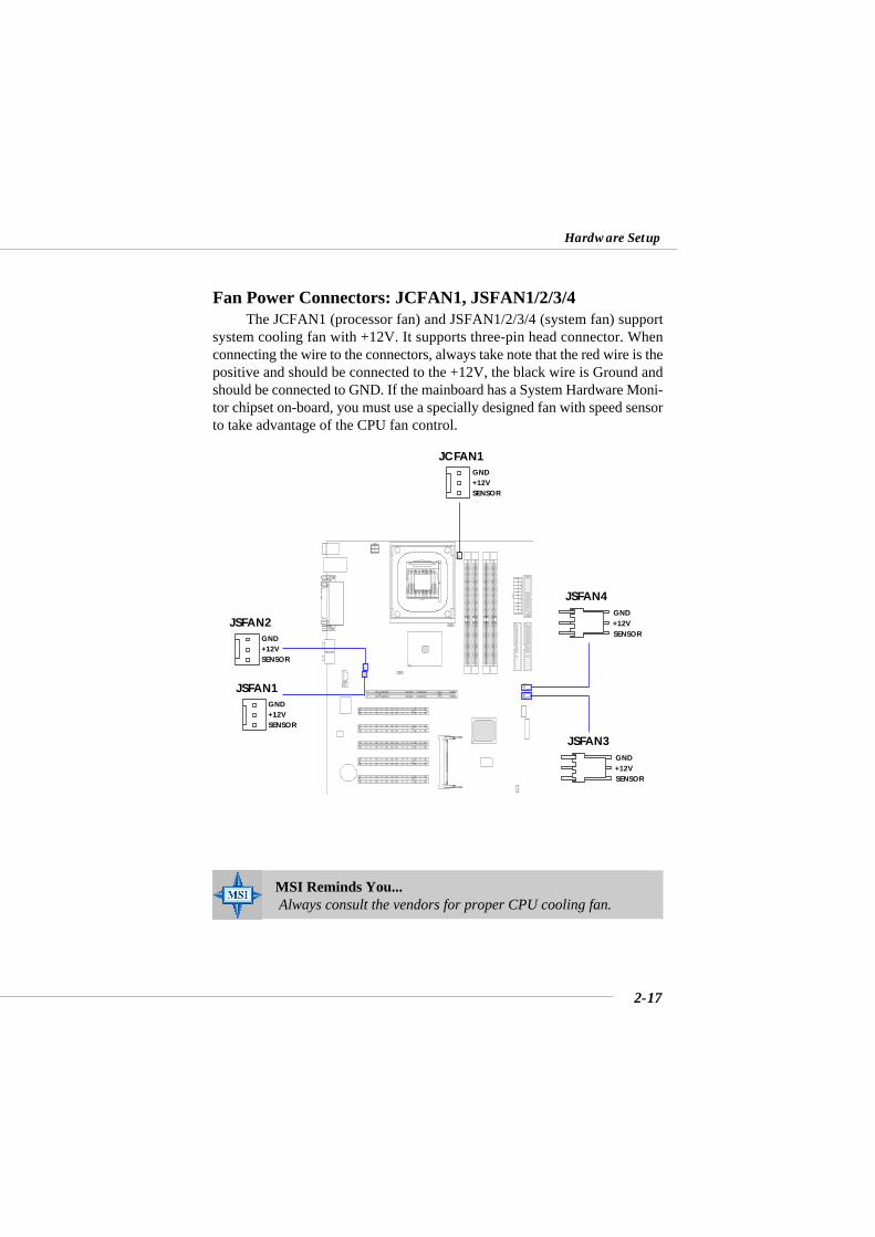
Hardware Setup
Fan Power Connectors: JCFAN1, JSFAN1/2/3/4The JCFAN1 (processor fan) and JSFAN1/2/3/4 (system fan) support
system cooling fan with +12V. It supports three-pin head connector. Whenconnecting the wire to the connectors, always take note that the red wire is thepositive and should be connected to the +12V, the black wire is Ground andshould be connected to GND. If the mainboard has a System Hardware Moni-tor chipset on-board, you must use a specially designed fan with speed sensorto take advantage of the CPU fan control.
MSI Reminds You... Always consult the vendors for proper CPU cooling fan.
SENSOR+12VGND
JSFAN2
SENSOR+12VGND
JCFAN1
SENSOR+12VGND
JSFAN4
SENSOR+12VGND
JSFAN3SENSOR+12VGND
JSFAN1

2-18
MS-9126 ATX Mainboard
Front Panel Connectors: JFP1The mainboard provides one front panel connector for electrical con-
nection to the front panel switches and LEDs.
9
10
JFP1
1
18
1415
PowerSwitch
PowerLED +
HDDLED
Keylock
ResetSwitch
+
Speaker
Buzzer

2-19
Hardware Setup
PIN SIGNAL PIN SIGNAL
1 USBPWR 2 GND
3 USBP2- 4 GND
5 USBP2+ 6 USBP3+
7 GND 8 USBP3-
9 GND 10 USBPWR
Pin Definition
Front USB Connector: JUSB1The mainboard provides one USB 2.0 pinheader for connection to addi-
tional USB ports. USB 2.0 technology increases data transfer rate up to amaximum throughput of 480Mbps, which is 40 times faster than USB 1.1,and is ideal for connecting high-speed USB interface peripherals such as USBHDD, digital cameras, MP3 players, printers, modems and the like.
JUSB11
9
2
10

2-20
MS-9126 ATX Mainboard
Chassis Intrusion Switch Connector: JINT1This connector is connected to a 2-pin chassis switch. If the chassis is
opened, the switch will be short. The system will record this status and showa warning message on the screen. To clear the warning, you must enter theBIOS utility and clear the record.
CD-In Connector: JCDIN1The connector is for CD-ROM audio connector.
JCDIN1
GND
R
L
JINT1
12
CINTRUGND

2-21
Hardware Setup
The motherboard provides the following jumpers for you to set thecomputer’s function. This section will explain how to change yourmotherboard’s function through the use of jumpers.
Clear CMOS Jumper: JCMOS1There is a CMOS RAM on board that has a power supply from external
battery to keep the data of system configuration. With the CMOS RAM, thesystem can automatically boot OS every time it is turned on. If you want toclear the system configuration, use the JCMOS1 (Clear CMOS Jumper ) toclear data. Follow the instructions below to clear the data:
Jumpers
MSI Reminds You...You can clear CMOS by shorting 2-3 pin while the system is off.Then return to 1-2 pin position. Avoid clearing the CMOS whilethe system is on; it will damage the mainboard.
Keep CMOS Clear CMOS
3
1
3
1
JCMOS11

2-22
MS-9126 ATX Mainboard
Slots
The motherboard provides one AGP Pro slot, five 32-bit Master PCIbus slots, and one Mini PCI slot.
PCI Slots
AGP (Accelerated Graphics Port) Pro SlotThe AGP Pro slot allows you to insert the AGP/AGP Pro graphics card.
AGP is an interface specification designed for the throughput demands of 3Dgraphics. It introduces a 66MHz, 32-bit channel for the graphics controller todirectly access main memory.
PCI (Peripheral Component Interconnect) SlotsThe PCI slots allow you to insert the expansion cards to meet your needs.
When adding or removing expansion cards, make sure that you unplug thepower supply first. Meanwhile, read the documentation for the expansion cardto make any necessary hardware or software settings for the expansion card,such as jumpers, switches or BIOS configuration. The mainboard providesfive 32-bit Master PCI bus slots and one Mini PCI slot.
AGP Pro Slot
Mini PCI Slot

2-23
Hardware Setup
Mini PCI bus: This bus is used to connect the optional MS-9518 SCSIcard.
Installing the card:
MS-9518 SCSI card
MSI Reminds You...You can barely see the golden finger if the card is properly inserted in the socket.
1. Locate the Mini PCI slot on themainboard.
Mini PCI slot
2. Place the card over the Mini PCI slotand gently insert both ends of the cardslantways (at an angle of 45 degrees)into the slot until the golden finger ofthe card gets fully inserted into the slot.

2-24
MS-9126 ATX Mainboard
3. Locate the supporters on themainboard (one on the right end andthe other on the left end).
supporters
5. Push the retaining clips (on two endsof the slot) inwards until they lock ontothe notches in the ends of the card. Thecard should securely fit into the slot.
4. Align the two fixing holes on thecard with the supporters and press thecard carefully down until the fixingholes get locked by the supporters.
Supporters lock into the fix-ing holes of the card.

2-25
Hardware Setup
Removing the card:1. Gently push the retaining clipsoutwards. Hold the card lightly butfirmly. Use long nose pliers to clip oneof the supporters and press it down-wards until it withdraws from the fix-ing hole.
2. Clip the other supporter and press itdownwards until it withdraws from thefixing hole.
3. The card will automatically boundupwards after being released from thesupporters.
4. Remove the card from the Mini PCIslot.

2-26
MS-9126 ATX Mainboard
PCI Interrupt Request RoutingThe IRQ, acronym of interrupt request line and pronounced I-R-Q, are
hardware lines over which devices can send interrupt signals to themicroprocessor. The PCI IRQ pins are typically connected to the PCI bus INTA# ~ INT D# pins as follows:
Order 1 Order 2 Order 3 Order 4
PCI Slot 1 INT A# INT B# INT C# INT D#
PCI Slot 2 INT B# INT C# INT D# INT A#
PCI Slot 3 INT C# INT D# INT A# INT B#
PCI Slot 4 INT D# INT A# INT B# INT C#
PCI Slot 5 INT B# INT C# INT D# INT A#

3-1
BIOS Setup
Chapter 3. BIOS Setup
This chapter provides information on the BIOS Setup pro-gram and allows you to configure the system for optimum use.You may need to run the Setup program when:
An error message appears on the screen during the systembooting up, and requests you to run SETUP.
You want to change the default settings for customizedfeatures.
BIOS Setup

3-2
MS-9126 ATX Mainboard
Entering Setup
Control Keys
Power on the computer and the system will start POST (Power On SelfTest) process. When the message below appears on the screen, press <DEL>key to enter Setup.
Press DEL to enter SETUP
If the message disappears before you respond and you still wish to enterSetup, restart the system by turning it OFF and On or pressing the RESETbutton. You may also restart the system by simultaneously pressing <Ctrl>,<Alt>, and <Delete> keys.
<↑> Move to the previous item
<↓> Move to the next item
<←> Move to the item in the left hand
<→> Move to the item in the right hand
<Enter> Select the item
<Esc> Jumps to the Exit menu or returns to the main menu from a submenu
<+/PU> Increase the numeric value or make changes
<-/PD> Decrease the numeric value or make changes
<F1> General help, only for Status Page Setup Menu and Option Page
Setup Menu
<F5> Restore the previous CMOS value from CMOS, only for Option Page
Setup Menu
<F6> Load the default CMOS value from Fail-Safe default table, only for
Option Page Setup Menu
<F7> Load Optimized defaults
<F10> Save all the CMOS changes and exit

3-3
BIOS Setup
Getting HelpAfter entering the Setup menu, the first menu you will see is the Main
Menu.
Main MenuThe main menu lists the setup functions you can make changes to. You
can use the arrow keys ( ↑↓ ) to select the item. The on-line description of thehighlighted setup function is displayed at the bottom of the screen.
Sub-MenuIf you find a right pointer symbol (as shown in the right view) appears
to the left of certain fields that means a sub-menu can be launched from this field. Asub-menu contains additional options for afield parameter. You can use arrow keys (↑↓ ) to highlight the field and press <Enter>to call up the sub-menu. Then you can usethe control keys to enter values and move from field to field within a sub-menu. If you want to return to the main menu, just press the <Esc >.
General Help <F1>The BIOS setup program provides a General Help screen. You can call
up this screen from any menu by simply pressing <F1>. The Help screen liststhe appropriate keys to use and the possible selections for the highlighteditem. Press <Esc> to exit the Help screen.
MSI Reminds You...The items under each BIOS category described in this chapterare under continuous update for better system performance.Therefore, the description may be slightly different from the lat-est BIOS and should be held for reference only.

3-4
MS-9126 ATX Mainboard
The Main Menu
Standard CMOS FeaturesUse this menu for basic system configurations, such as time, date etc.
Advanced BIOS FeaturesUse this menu to configure the special enhanced features.
Advanced Chipset FeaturesUse this menu to change the values in the chipset registers and optimize yoursystem’s performance.
Integrated PeripheralsUse this menu to specify your settings for integrated peripherals.
Power Management SetupUse this menu to specify your settings for power management.
Once you enter AwardBIOS CMOS Setup Utility, the Main Menu willappear on the screen. The Main Menu displays twelve configurable functionsand two exit choices. Use arrow keys to move among the items and press<Enter> to enter the sub-menu.

3-5
BIOS Setup
PNP/PCI ConfigurationsThis entry appears if your system supports PnP/PCI.
PC Health StatusThis entry shows your PC health status.
Frequency/Voltage ControlUse this menu to specify your settings for frequency/voltage control.
Load Fail-Safe DefaultsUse this menu to load the BIOS default values for minimal but stable systemperformance.
Load Optimized DefaultsUse this menu to load the BIOS default values that are factory settings foroptimal system operations.
Set Supervisor/User PasswordUse this menu to set user and supervisor passwords.
Save & Exit SetupSave changes to CMOS and exit setup.
Exit Without SavingAbandon all changes and exit setup.

3-6
MS-9126 ATX Mainboard
Standard CMOS FeaturesThe items inside Standard CMOS Features menu are divided into 10
categories. Each category includes none, one or more setup items. Use thearrow keys to highlight the item you want to modify and use the <PgUp> or<PgDn> keys to switch to the value you prefer.
Date (mm:dd:yy)This allows you to set the system to the date that you want (usually the currentdate). The format is <day><month> <date> <year>.
day Day of the week, from Sun to Sat, determined byBIOS. Read-only.
month The month from Jan. through Dec.date The date from 1 to 31 can be keyed by numeric
function keys.year The year can be adjusted by users.
Time (hh:mm:ss)This allows you to set the system time that you want (usually the currenttime). The time format is <hour> <minute> <second>.
IDE Primary/Secondary Master/SlavePress PgUp/<+> or PgDn/<-> to select Manual, None, Auto type. Note thatthe specifications of your drive must match with the drive table. The hard disk

3-7
BIOS Setup
will not work properly if you enter improper information for this category. Ifyour hard disk drive type is not matched or listed, you can use Manual todefine your own drive type manually.If you select Manual, related information is asked to be entered to the follow-ing items. Enter the information directly from the keyboard. This informationshould be provided in the documentation from your hard disk vendor or thesystem manufacturer.If the controller of HDD interface is SCSI, the selection shall be “None”. Ifthe controller of HDD interface is CD-ROM, the selection shall be “None”.
Access Mode The settings are CHS, LBA, Large, Auto.Capacity The formatted size of the storage device.Cylinder Number of cylinders.Head Number of heads.Precomp Write precompensation.Landing Zone Cylinder location of the landing zone.Sector Number of sectors.
Drive A/BThis item allows you to set the type of floppy drives installed. Availableoptions are None, 360K, 5.25 in., 1.2M, 5.25 in., 720K, 3.5 in., 1.44M, 3.5 in.,2.88M, 3.5 in.
VideoThe setting controls the type of video adapter used for the primary monitor ofthe system. Available options are EGA/VGA , CGA 40, CGA 80 and Mono.
Halt OnThe setting determines whether the system will stop if an error is detected atboot. Available options are:
All Errors The system stops when any error is detected.No Errors The system doesn’t stop for any detected error.All, But Keyboard The system doesn’t stop for a keyboard error.All, But Diskette The system doesn’t stop for a disk error.All, But Disk/Key The system doesn’t stop for either a disk or a key-
board error.
Base/Extended/Total MemoryThe three items show the memory status of the system. (Read only)

3-8
MS-9126 ATX Mainboard
Advanced BIOS Features
Virus WarningThe item is to set the Virus Warning feature for IDE Hard Disk boot sectorprotection. If the function is enabled and any attempt to write data into thisarea is made, BIOS will display a warning message on screen and beep. Set-ting options: Disabled, Enabled.
BIOS Flash Write ControlThis function protects the BIOS from accidental corruption by unauthorizedusers or computer viruses. When disabled, the BIOS' data cannot be changedwhen attempting to update the BIOS with a Flash utility. To successfullyupdate the BIOS, you'll need to enable this BIOS Flash Write Control function.Setting options: Disabled, Enabled.
CPU L1 & L2 CacheCache memory is additional memory that is much faster than conventionalDRAM (system memory). When the CPU requests data, the system transfersthe requested data from the main DRAM into cache memory, for even fasteraccess by the CPU. The settings enable/disable the internal cache (also knownas L1 or level 1 cache) and external cache (also known as L2 or level 2 cache).Setting options: Disabled, Enabled.

3-9
BIOS Setup
Quick Power On Self TestThe option speeds up Power On Self Test (POST) after you power on thecomputer. When setting the item to Enabled, BIOS will shorten or skip somecheck items during POST. Settings: Enabled, Disabled.
First/Second/Third Boot DeviceThe items allow you to set the sequence of boot devices where BIOS attemptsto load the disk operating system. The settings are:
Floppy The system will boot from floppy drive.LS120 The system will boot from LS-120 drive.Hard Disk The system will boot from the HDD.CDROM The system will boot from the CD-ROM.ZIP100 The system will boot from ATAPI ZIP drive.USB-FDD The system will boot from the floppy drive at USB ports.LAN The system will boot from the Network drive.Disabled Disable this sequence.
Boot Other DeviceSetting the option to Enabled allows the system to try to boot from otherdevices if the system fails to boot from the 1st/2nd/3rd boot device.
Swap Floppy DriveSetting to Enabled will swap floppy drives A: and B:.
Boot Up Floppy SeekThis setting causes the BIOS to search for floppy disk drives at boot time.When enabled, the BIOS will activate the floppy disk drives during the bootprocess: the drive activity light will come on and the head will move back andforth once. First A: will be done and then B: if it exists. Setting options:Disabled, Enabled.
Boot Up NumLock StatusThis setting is to set the Num Lock status when the system is powered on.
MSI Reminds You...Available settings for “First/Second/Third Boot Device” varydepending on the bootable devices you have installed. Forexample, if you did not install a floppy drive, the setting “Floppy”does not show up.

3-10
MS-9126 ATX Mainboard
Setting to On will turn on the Num Lock key when the system is powered on.Setting to Off will allow users to use the arrow keys on the numeric keypad.Setting options: On, Off.
Gate A20 OptionThis item is to set the Gate A20 status. A20 refers to the first 64KB of ex-tended memory. When the default value Fast is selected, the Gate A20 iscontrolled by Port92 or chipset specific method resulting in faster systemperformance. When Normal is selected, A20 is controlled by a keyboard con-troller or chipset hardware.
Typematic Rate SettingThis item is used to enable or disable the typematic rate setting includingTypematic Rate & Typematic Delay.
Typematic Rate (Chars/Sec)After Typematic Rate Setting is enabled, this item allows you to set the rate(characters/second) at which the keys are accelerated. Settings: 6, 8, 10, 12,15, 20, 24 and 30.
Typematic Delay (Msec)This item allows you to select the delay between when the key was first pressedand when the acceleration begins. Settings: 250, 500, 750 and 1000.
Security OptionThis specifies the type of BIOS password protection that is implemented. Set-tings are described below:
APIC ModeThis setting is used to enable or disable the APIC (Advanced ProgrammableInterrupt Controller). Due to compliance to PC2001 design guide, the systemis able to run in APIC mode. Enabling APIC mode will expand availableIRQs resources for the system. Setting options: Enabled, Disabled.
Option DescriptionSetup The password prompt appears only when end users try to
run Setup.
System A password prompt appears every time when the com-puter is powered on or when end users try to run Setup.

3-11
BIOS Setup
MPS Version Control For OSThis field allows you to select which MPS (Multi-Processor Specification)version to be used for the operating system. You need to select the MPS ver-sion supported by your operating system. To find out which version to use,consult the vendor of your operating system. Settings: 1.4, 1.1.
OS Select For DRAM > 64MBThis allows you to run the OS/2® operating system with DRAM larger than64MB. When you choose Non-OS2, you cannot run the OS/2® operatingsystem with DRAM larger than 64MB. But it is possible if you choose OS2.
Report No FDD For WIN 95For compatibility with Windows 95 logo certification, select Yes to releaseIRQ6 when the system contains no floppy drive. When this setting is set toYes, users have to select Disabled for the Onboard FDC Controller in theIntegrated Peripherals menu. Setting options: Yes, No.
Small Logo(EPA) ShowThis item enables you to show the EPA logo (brand specific graphics) on thebootup screen. Settings are:
Disabled Shows the normal POST screen at boot.Enabled Shows a still image (EPA logo) on the screen at boot.

3-12
MS-9126 ATX Mainboard
Advanced Chipset Features
DRAM Timing ControlPress <Enter> to enter the sub-menu and the following screen appears:
DRAM Freq. ControlUse this setting to configure the clock frequency of the installed DRAM.
MSI Reminds You...Change these settings only if you are familiar with the chipset.

3-13
BIOS Setup
When set to Default, the DRAM frequency will be automaticallyconfigured according to the CPU clock (400MHz CPU => 200MHzDRAM, 533MHz CPU => 266MHz DRAM). Setting options: Default,200MHz, 266MHz.
DRAM Timing ConfigureThis setting determines whether DRAM timing is configured by readingthe contents of the SPD (Serial Presence Detect) EEPROM on the DRAMmodule. Selecting By SPD makes the following settings automaticallydetermined by BIOS according to the configurations on the SPD. Settingoptions: By SPD, Manual.
CAS Latency TimeThis controls the timing delay (in clock cycles) before DRAM starts aread command after receiving it. Settings: 1.5, 2, 2.5 (clocks). 1.5 (clocks)increases the system performance the most while 2.5 (clocks) providesthe most stable performance.
Active to Precharge DelayThis setting controls the number of clock cycles for DRAM to be al-lowed to precharge from the active state. Setting options: 7, 6, 5.
DRAM RAS# to CAS# DelayWhen DRAM is refreshed, both rows and columns are addressedseparately. This setup item allows you to determine the timing of thetransition from RAS (row address strobe) to CAS (column address strobe).The less the clock cycles, the faster the DRAM performance. Settingoptions: 3, 2.
DRAM RAS# PrechargeThis item controls the number of cycles for Row Address Strobe (RAS)to be allowed to precharge. If insufficient time is allowed for the RAS toaccumulate its charge before DRAM refresh, refresh may be incompleteand DRAM may fail to retain data. This item applies only when synchro-nous DRAM is installed in the system. Setting options: 2, 3.
DRAM Read Thermal MgmtThis setting is used to activate the thermal management mechanism forDRAM read actions. Setting options: Enabled, Disabled.

3-14
MS-9126 ATX Mainboard
DRAM Data Integrity ModeSelect ECC (Error-Checking & Correcting Code) or Non-ECC according tothe type of DRAM installed.
System BIOS CacheableSelecting Enabled allows caching of the system BIOS ROM at F0000h-FFFFFh, resulting in better system performance. However, if any programwrites to this memory area, a system error may result. Setting options: Enabled,Disabled.
Video BIOS CacheableSelecting Enabled allows caching of the video BIOS ROM at C0000h toC7FFFh, resulting in better video performance. However, if any program writesto this memory area, a system error may result. Setting options: Disabled,Enabled.
Memory Hole At 15M-16MIn order to improve performance, certain space in memory can be reservedfor ISA cards. This memory must be mapped into the memory space below16MB. When this area is reserved, it cannot be cached. Setting options:Disabled, Enabled.
Delayed TransactionThe chipset has an embedded 32-bit posted write buffer to support delayedtransactions cycles so that transactions to and from the ISA bus are bufferedand PCI bus can perform other transactions while the ISA transaction isunderway. Select Enabled to support compliance with PCI specification ver-sion 2.1. Setting options: Enabled, Disabled.
Delay Prior to ThermalWhen the CPU temperature reaches a factory preset level, a thermal monitor-ing mechanism will be enabled following the appropriate timing delay speci-fied in this field. With the thermal monitoring enabled, clock modulationcontrolled by the processor’s internal thermal sensor is also activated to keepthe processor within allowable temperature limit. Setting options: 4 Min, 8Min, 16 Min, 32 Min.
AGP Aperture Size (MB)This setting controls just how much system RAM can be allocated to AGP for

3-15
BIOS Setup
video purposes. The aperture is a portion of the PCI memory address rangededicated to graphics memory address space. Host cycles that hit the aperturerange are forwarded to the AGP without any translation. The option allowsthe selection of an aperture size of 4, 8, 16, 32, 64, 128, and 256 (MB).
Init Display FirstThis setting specifies which VGA card is your primary graphics adapter. Set-ting options: PCI Slot, AGP.

3-16
MS-9126 ATX Mainboard
Integrated Peripherals
OnChip IDE DevicePress <Enter> to enter the sub-menu and the following screen appears:
IDE HDD Block ModeThis allows your hard disk controller to use the fast block mode to trans-fer data to and from the hard disk drive. Block mode is also called blocktransfer, multiple commands or multiple sector read/write. Enabled ena-bles IDE controller to use block mode; Disabled allows the controller touse standard mode.

3-17
BIOS Setup
On-Chip Primary/Secondary PCI IDEThe integrated peripheral controller contains an IDE interface with sup-port for two IDE channels. Choose Enabled to activate each channelseparately.
IDE Primary/Secondary Master/Slave PIOThe four items allow you to set a PIO (Programmed Input/Output) modefor each of the four IDE devices that the onboard IDE interface supports.Modes 0~4 provide increased performance. In Auto mode, BIOS auto-matically determines the best mode for each IDE device.
IDE Primary/Secondary Master/Slave UDMAUltra DMA implementation is possible only if your IDE device supportsit and your operating environment contains a DMA driver. If both yourhard drive and software support Ultra DMA 33 (or higher), select Autoto enable BIOS support.
Onboard DevicePress <Enter> to enter the sub-menu and the following screen appears:
USB ControllerSelect Enabled if your system contains a Universal Serial Bus (USB)controller and you have USB peripherals. Setting options: Enabled,Disabled.
USB 2.0 SupportThis setting disables/enables the support for USB 2.0 technology. USB

3-18
MS-9126 ATX Mainboard
2.0 technology increases data transfer rate up to a maximum throughputof 480Mbps, which is 40 times faster than USB 1.1 and is ideal for con-necting high-speed USB interface peripherals such as USB HDD, digitalcameras, MP3 players, printers, modems and the like. Setting options:Disabled, Enabled.
USB Keyboard SupportSet to Enabled if your need to use an USB keyboard in the operatingsystem that does not support or have any USB driver installed, such asDOS and SCO Unix.
AC’97 AudioThis setting is used to enable or disable the onboard AC’97 (AudioCodec’97) feature. Selecting Auto allows the mainboard to detect whetheran audio device is used. If an audio device is detected, the onboard AC’97controller will be enabled; if not, the controller is disabled. Disable thefunction if you want to use other controller cards to connect an audiodevice. Setting options: Disabled and Auto.
Super IO DevicePress <Enter> to enter the sub-menu and the following screen appears:
Onboard FDC ControllerSelect Enabled if your system has a floppy disk controller (FDD) in-stalled on the system board and you wish to use it. If you install add-onFDC or the system has no floppy drive, select Disabled in this field. Thesettings are: Enabled and Disabled.

3-19
BIOS Setup
Onboard Serial Port 1/Port 2Select an address and corresponding interrupt for the first and secondserial ports. The settings are: 3F8/IRQ4, 2E8/IRQ3, 3E8/IRQ4, 2F8/IRQ3,Disabled, Auto.
Onboard Parallel PortThere is a built-in parallel port on the on-board Super I/O chipset thatprovides Standard, ECP, and EPP features. It has the following options:
Disabled3BC/IRQ7 Line Printer port 0278/IRQ5 Line Printer port 2378/IRQ7 Line Printer port 1
Parallel Port ModeSPP: Standard Parallel PortEPP: Enhanced Parallel PortECP: Extended Capability PortECP + EPP: Extended Capability Port + Enhanced Parallel PortTo operate the onboard parallel port as Standard Parallel Port only, choose“SPP.” To operate the onboard parallel port in the EPP modesimultaneously, choose “EPP.” By choosing “ECP”, the onboard paral-lel port will operate in ECP mode only. Choosing “ECP + EPP” willallow the onboard parallel port to support both the ECP and EPP modessimultaneously.
EPP Mode SelectThe onboard parallel port is EPP Spec. compliant, so after the user choosesthe onboard parallel port with the EPP function, the following messagewill be displayed on the screen: “EPP Mode Select.” At this time eitherEPP 1.7 spec or EPP 1.9 spec can be chosen.
ECP Mode Use DMAThe ECP mode has to use the DMA channel, so choose the onboardparallel port with the ECP feature. After selecting it, the following mes-sage will appear: “ECP Mode Use DMA.” At this time, the user canchoose between DMA channel 3 or 1.

3-20
MS-9126 ATX Mainboard
PWRON After PWR-FailThis setting specifies whether your system will reboot after a power fail-ure or interrupts occurs. Available settings are:
Off Leaves the computer in the power off state.On Reboots the computer.Former-Sts Restores the system to the status before power failure or
interrupt occurs.
Power Status LEDThis setting configures how the system uses power LED on the case toindicate the sleep state. Available options are:
Single The power LED blinks to indicate the sleep state without changing its color.
Dual The power LED changes its color to indicate the sleepstate.

3-21
BIOS Setup
Power Management Setup
ACPI FunctionThis item is to activate the ACPI (Advanced Configuration and Power Man-agement Interface) function. If your operating system is ACPI-aware, such asWindows 98SE/2000/ME, select Enabled. Setting options: Enabled, Disabled.
ACPI Standby StateThis item specifies the power saving modes for ACPI function. If your oper-ating system supports ACPI, such as Windows 98SE, Windows ME and Win-dows 2000, you can choose to enter the Standby mode in S1(POS) or S3(STR) fashion through the setting of this field. Options are:
S1(POS) The S1 sleep mode is a low power state. In this state, nosystem context is lost (CPU or chipset) and hardwaremaintains all system context.
MSI Reminds You...S3-related functions described in this section are available onlywhen your BIOS supports S3 sleep mode.

3-22
MS-9126 ATX Mainboard
S3(STR) The S3 sleep mode is a lower power state where the information of system configuration and open applications/files is saved to main memory that remains poweredwhile most other hardware components turn off to saveenergy. The information stored in memory will be usedto restore the system when a “wake up” event occurs.
S1 & S3 BIOS determines the best mode automatically.
Run VGA BIOS If S3 ResumeSelecting Enabled allows BIOS to call VGA BIOS to initialize the VGA cardwhen system wakes up (resumes) from S3 sleep state. The system resumetime is shortened when you disable the function, but system will need an AGPdriver to initialize the VGA card. Therefore, if the AGP driver of the carddoes not support the initialization feature, the display may work abnormallyor not function after resuming from S3.
Power ManagementThis item is used to select the degree (or type) of power saving and is relatedto these modes: Suspend Mode and HDD Power Down. There are three op-tions for power management:
Min Saving Minimum Power Management. Suspend Mode = 1 Hour.Max Saving Maximum Power Management. Suspend Mode = 1 Min.User Define Allows end users to configure each mode separately.
Video Off MethodThis determines the manner in which the monitor is blanked.
V/H SYNC+Blank This selection will cause the system to turn offthe vertical and horizontal synchronization portsand write blanks to the video buffer.
Blank Screen This option only writes blanks to the video buffer.DPMS Initial display power management signaling.
Video Off In SuspendThis setting determines whether the monitor will be turned off during suspendmode. Setting options: Yes, No.
Modem Use IRQName the interrupt request (IRQ) line assigned to the modem (if any) on your

3-23
BIOS Setup
system. Activity of the selected IRQ always awakens the system. Settings are3, 4, 5, 7, 9, 10, 11 and NA.
Suspend ModeIf system activity is not detected for the length of time specified in this field,all devices except CPU will be shut off. Settings are Disabled, 1 Min, 2 Min,4 Min, 8 Min, 12 Min, 20 Min, 30 Min, 40 Min and 1 Hour.
HDD Power DownWhen enabled and after the set time of system inactivity, the hard disk drivewill be powered down while all other devices remain active. The settings are:Disable, 1~15 Min.
Soft-Off by PWR-BTTNThis feature allows users to configure the power button function. Settings are:
Instant-Off The power button functions as a normal power-on/-off button.
Delay 4 Sec. When you press the power button, the computer en-ters the suspend/sleep mode, but if the button ispressed for more than four seconds, the computer isturned off.
CPU THRM-ThrottlingThe item allows you to specify the CPU speed (at percentage) to which it willslow down when the CPU reaches the predetermined overheat temperature.Settings range from 12.5% to 87.5% at 12.5% increment.
Wake Up By PCI Card, USB KB Wake Up From S3These settings specify whether the system will be awakened from power sav-ing modes when activity or input signal of the specified hardware peripheralor component is detected. Setting options: Enabled, Disabled.
Resume By AlarmThe field is used to enable or disable the feature of booting up the system ona scheduled time/date.
Date (of Month) AlarmThe field specifies the date for Resume by Alarm. Settings: 0~31.

3-24
MS-9126 ATX Mainboard
Time (hh:mm:ss) AlarmThe field specifies the time for Resume by Alarm. Format is <hour><minute><second>.
Reload Global Timer Events: Primary IDE 0/1, Secondary IDE 0/1, FDD/COM/LPT Port, PCI PIRQ [A-D]#Global Timer Events are I/O events whose occurrence can prevent the systemfrom entering a power saving mode or can awaken the system from such amode. In effect, the system remains alert for anything which occurs to a de-vice that is configured as Enabled, even when the system is in a power downmode.
MSI Reminds You...If you have changed this setting, you must let the system boot upuntil it enters the operating system, before this function will work.

3-25
BIOS Setup
PNP/PCI Configurations
This section describes configuring the PCI bus system and PnP (Plug &Play) feature. PCI, or Peripheral Component Interconnect, is a system whichallows I/O devices to operate at speeds nearing the speed the CPU itself useswhen communicating with its special components. This section covers somevery technical items and it is strongly recommended that only experiencedusers should make any changes to the default settings.
Reset Configuration DataNormally, you leave this field Disabled. Select Enabled to reset ExtendedSystem Configuration Data (ESCD) when you exit Setup if you have installeda new add-on card and the system reconfiguration has caused such a seriousconflict that the operating system cannot boot. Setting options: Enabled,Disabled.
Resource Controlled ByThe Award Plug and Play BIOS has the capacity to automatically configureall of the boot and Plug and Play compatible devices. However, this capabilitymeans absolutely nothing unless you are using a Plug and Play operating sys-tem such as Windows® 95/98. If you set this field to “manual” choose specificresources by going into each of the sub menu that follows this field (a submenu is preceded by a “ ”). The settings are: Auto (ESCD), Manual.

3-26
MS-9126 ATX Mainboard
IRQ ResourcesThe items are adjustable only when Resources Controlled By is set to Manual.Press <Enter> and you will enter the sub-menu of the items. IRQ Resourceslist IRQ 3/4/5/7/9/10/11/12/14/15 for users to set each IRQ a type dependingon the type of device using the IRQ. Settings are:
PCI Device For Plug & Play compatible devices designed for PCIbus architecture.
Reserved The IRQ will be reserved for further request.
PCI/VGA Palette SnoopWhen set to Enabled, multiple VGA devices operating on different buses canhandle data from the CPU on each set of palette registers on every videodevice. Bit 5 of the command register in the PCI device configuration space isthe VGA Palette Snoop bit (0 is disabled). For example, if there are two VGAdevices in the computer (one PCI and one ISA) and the:
The setting must be set to Enabled if any ISA bus adapter in the system re-quires VGA palette snooping.
VGA Palette Snoop Bit Setting Action
Disabled Data read or written by the CPU is only directed to the PCIVGA device’s palette registers.
Enabled Data read or written by the CPU is directed to both the PCIVGA device’s palette registers and the ISA VGA device’spalette registers, permitting the palette registers of both VGAdevices to be identical.

3-27
BIOS Setup
PC Health Status
This section shows the status of your CPU, fan, overall system status,etc. Monitor function is available only if there is hardware monitoring mecha-nism onboard.
Chassis Intrusion DetectThe field enables or disables the feature of recording the chassis intrusionstatus and issuing a warning message if the chassis is once opened. To clearthe warning message, set the field to Reset. The setting of the field will auto-matically return to Enabled later. Setting options: Enabled, Reset, Disabled.
CPU Temperature LimitIf the CPU temperature reaches the upper limit preset in this setting, the warn-ing mechanism will be activated. This helps you to prevent the CPU overheatproblem.
Current System/CPU Temperature, CPU/Power/System Fan, Vcore(V),VDDQ(V), +3.3(V), +5V, +12V, -12V, -5V, VBAT(V), 5VSB(V)These items display the current status of all of the monitored hardware de-vices/components such as CPU voltages, temperatures and all fans’ speeds.
Shutdown TemperatureThis option is for setting the shutdown temperature level for the processor.When the processor reaches the temperature you set, the system will be shutdown.

3-28
MS-9126 ATX Mainboard
Use this menu to specify your settings for frequency/voltage control.
CPU Clock RatioThis setting controls the multiplier that is used to determine the internal clockspeed of the processor relative to the external or motherboard clock speed.
Auto Detect PCI ClkThis item is used to auto detect the PCI slots. When set to Enabled, the systemwill remove (turn off) clocks from empty PCI slots to minimize the electro-magnetic interference (EMI). Setting options: Enabled, Disabled.
Spread SpectrumWhen the motherboard’s clock generator pulses, the extreme values (spikes)of the pulses creates EMI (Electromagnetic Interference). The Spread Spec-trum function reduces the EMI generated by modulating the pulses so that thespikes of the pulses are reduced to flatter curves. If you do not have any EMIproblem, leave the setting at Disabled for optimal system stability andperformance. But if you are plagued by EMI, setting to Enabled for EMIreduction. Remember to disable Spread Spectrum if you are overclockingbecause even a slight jitter can introduce a temporary boost in clockspeedwhich may just cause your overclocked processor to lock up.
Frequency/Voltage Control

3-29
BIOS Setup
Load Fail-Safe/Optimized Defaults
When you select Load Optimized Defaults, a message as below appears:
Pressing Y loads the default factory settings for optimal systemperformance.
The two options on the main menu allow users to restore all of the BIOSsettings to the default Fail-Safe or Optimized values. The Optimized Defaultsare the default values set by the mainboard manufacturer specifically for op-timal performance of the mainboard. The Fail-Safe Defaults are the defaultvalues set by the BIOS vendor for stable system performance.
When you select Load Fail-Safe Defaults, a message as below appears:
Pressing Y loads the BIOS default values for the most stable, minimalsystem performance.

3-30
MS-9126 ATX Mainboard
Set Supervisor/User Password
MSI Reminds You...About Supervisor Password & User Password:Supervisor password: Can enter and change the settings of
the setup menu.User password: Can only enter but do not have the
right to change the settings of the setupmenu.
When you select this function, a message as below will appear on thescreen:
Type the password, up to six characters in length, and press <Enter>.The password typed now will replace any previously set password from CMOSmemory. You will be prompted to confirm the password. Retype the pass-word and press <Enter>. You may also press <Esc> to abort the selection andnot enter a password.
To clear a set password, just press <Enter> when you are prompted toenter the password. A message will show up confirming the password will bedisabled. Once the password is disabled, the system will boot and you canenter Setup without entering any password.
When a password has been set, you will be prompted to enter it everytime you try to enter Setup. This prevents an unauthorized person from chang-ing any part of your system configuration.
Additionally, when a password is enabled, you can also have AwardBIOS to request a password each time the system is booted. This would pre-vent unauthorized use of your computer. The setting to determine when thepassword prompt is required is the Security Option of the ADVANCED BIOSFEATURES menu. If the Security Option is set to System, the password isrequired both at boot and at entry to Setup. If set to Setup, password promptonly occurs when you try to enter Setup.

T-1
Troubleshooting
Troubleshooting
Troubleshooting
Q: Where can I find the model number of the mainboard?A: There are two places where you can find the model number of the mainboard:
1. Somewhere between the PCI slots you shall find MS-xxxx or the marketingname like “K7T Turbo”. You can also find the version number beside it. 2. Atthe back cover of the user's manual.
Q: What do you mean by PCB version 1?A: PCB is printed circuit board. Saying PCB version 1 is the same as saying
motherboard version 1.
Q: Why is my motherboard BIOS sticker "Phoenix BIOS" while I see "AwardBIOS" during system boot-up?
A: Phoenix & Award already merged as one company. All MSI motherboardsusing Award BIOS come with Phoenix logo stickers.
Q: How do I know what MSI D-LED or D-bracket light mean?A: Please follow the special tech issue, http://www.msi.com.tw/support/
techexpress/special_tech/smartled.htm
Q: I used my MSI motherboard and got an error message, "Primary IDEChannel No 80 Conductor Cable Installed" while the system detectedhard drives.
A: This is not a problem. It merely means that you're using an ATA-66 or ATA-100 HDD, but you're using the conductor 40 ATA-33 cable.
Q: I have high speed CPU cooling fan like Taisol CGK760092, Vantec CCK-6035D & GlobalWin WBK38. Can I install the fan directly to themotherboard?

T-2
MS-9126 ATX Mainboard
A: We strongly recommend that you do NOT connect those described CPUfan directly to your motherboard, as it draws so much power, that it coulddamage it. Please use a 3-Pin to 4-Pin Cable that comes together with the fan.
Q: Can I use more than 512MB memory on Win9x or WinME?A: No, you can’t. You can only use more than 512MB memory on Win2000 or
WinXP. This is a Microsoft OS issue. Please check http://support/microsoft.com/support/kb/articles/Q108/0/79.ASP
Q: I have tried to download the MSI Live Update utility from http://www.msi.com.tw/support/liveupdate/livedriver.htm but it keeps on failing?
A: This can be solved by one of the following suggestions: 1. Dont installzonealarm 2. Disable "WebTrap" of PC-cillion 2000 3. Disable any web basedanti-virus Software.
Q: Can Live Update Series support WinXP?A: Live Update Series version 215 can support WinXP. Download it from http:/
/www.msi.com.tw/support/liveupdate/livedriver.htm
Q: After flashing the BIOS, my system for unknown reason fails to boot.What should I do?
A: Please refer to the following suggestions: 1. Try the BIOS boot recoveryfeature as described in http://www.msi.com.tw/support/bios/boot.htm 2. Tryto clear the CMOS If problem still persists, ask your reseller for new BIOSchip or contact one of MSI office near your place for new BIOS chip http://www.msi.com.tw/contact/main.htm
Q: Should I update my BIOS, once a new BIOS is released?A: A new BIOS is usually released due to the following reasons:
1. New function is supported

T-3
Troubleshooting
2. New BIOS source code3. Bugs are found4. Customer-specific requestWhen we release a new BIOS, there's usually a release note attached whichlists the reason for the release. Refer to this release note and decide foryourself if upgrading to the new BIOS will be worth it. A word of advice,though, do not upgrade to the new BIOS, unless you really have to.
Q: How do I update the BIOS?A: Please refer to http://www.msi.com.tw/support/bios/note.htm for details.
Q: How do I identify the BIOS version?A: Upon boot-up, the 1st line appearing after the memory count is the BIOS
version. It is usually in the format:1. For older model number:AG76 091096 where:1st digit refers to BIOS maker as A = AMI(R) W = AWARD(R) P = PHOENIX(R).2nd digit refers to the internal chipset code.3rd digit refers to the processor class as 5 = 486, 7 = 586, 8 = 686.4th digit is incremental.091096 refers to the date this BIOS is released.2. For newer model number:W5139MS V1.0 091096 where:1st digit refers to BIOS maker as A = AMI(R) W = AWARD(R) P = PHOENIX(R).2nd - 5th digit refers to the model number.6th - 7th digit refers to the customer as MS = all standard customers.V1.0 refers to the BIOS version.091096 refers to the date this BIOS is released.

T-4
MS-9126 ATX Mainboard
Q: After I flashed the BIOS and rebooted the system, the screen went blank.A: For AMI BIOS
Rename the desired AMI BIOS file to AMIBOOT.ROM and save it on afloppy disk. e.g. Rename A569MS23.ROM to AMIBOOT.ROMInsert this floppy disk in the floppy drive. Turn On the system and pressand hold Ctrl-Home to force update. It will read the AMIBOOT.ROM fileand recover the BIOS from the A drive.When 4 beeps are heard you may remove the floppy disk and restart thecomputer.
For Award BIOSMake a bootable floopy diskCopy the Award flash utility & BIOS file to the said floppy diskCreate an autoexec.bat with "awdfl535 biosfilename" in the content e.g.awdfl535 a619mj21.binBoot up system with the said floppy (it will take less than 2 minutes beforescreen comes out)Re-flash the BIOS & reboot.

G-1
Glossary
GlossaryGlossary
ACPI (Advanced Configuration & Power Interface)This power management specification enables the OS (operating system) to control theamount of power given to each device attached to the computer. Windows 98/98SE,Windows 2000 and Windows ME can fully support ACPI to allow users managing thesystem power flexibly.
AGP (Accelerated Graphics Port)A new, high-speed graphics interface that based on PCI construction and designedespecially for the throughput demands of 3-D graphics. AGP provides a direct channel(32-bit wide bus) between the display controller and main memory for high graphicsquality and performance.
BluetoothBluetooth refers to a worldwide standard for the wireless exchange of data between twodevices. Bluetooth requires that a low-cost transceiver chip be included in each device.The tranceiver transmits and receives in a previously unused frequency band of 2.45GHz that is available globally (with some variation of bandwidth in different countries).In addition to data, up to three voice channels are available. Each device has a unique 48-bit address from the IEEE 802 standard. Connections can be point-to-point ormultipoint. The maximum range is 10 meters. Data can be exchanged at a rate of 1megabit per second (up to 2 Mbps in the second generation of the technology).
BIOS (Basic Input/Output System)On PCs, an essential software that contains all the control code of input/output inter-face (such as keyboard, disk drives, etc.). It executes hardware test on booting thesystem, starts the OS, and provides an interface between the OS and the components.The BIOS is stored in a ROM chip.
BusA set of hardware lines within the computer system, through which the data is trans-ferred among different components. In a PC, the term bus usually refers to a local busthat connects the internal components to the CPU and main memory.
CacheA special memory subsystem that is used to speed up the data transfer. It stores the

G-2
MS-9126 ATX Mainboard
Dynamic RAM (DRAM) Memory Technologies Type
FPM (60,70ns)EDO (50,60,70ns)SDRAM (66MHz)SDRAM (100MHz)SDRAM (133MHz)RDRAM (Direct Rambus)DDR SDRAM (100MHz)DDR SDRAM (133MHz)
First Used
1990 1994 1996 1998 1999 1999 2000 2000
Clock Rate
25MHz 40MHz 66MHz 100MHz 133MHz 400MHz 100MHz 133MHz
Bus* Width
64 bits 64 bits 64 bits 64 bits 64 bits 16 bits 64 bits 64 bits
Bandwidth 200 MBps 320 MBps 528 MBps 800 MBps 1.1 GBps 1.6 GBps 1.6 GBps 2.1 GBps
Volts
5v 5v 3.3v 3.3v 3.3v 2.5v 3.3v 3.3v
Peak
* Memory channel width (64 bits started with 75MHz Pentium)
Source: Computer Desktop Encyclopedia
contents of frequently accessed RAM locations and the addresses where these dataitems are stored.
ChipsetA collection of integrated chips designed to perform one or more related functions. Forexample, a modem chipset contains all the primary circuits for transmitting and receiv-ing data; a PC chipset provides the electronic interfaces between all subsystems.
Clock CycleClock cycle (or tick) is the smallest unit of time recognized by a device. For personalcomputers, clock cycles generally refer to the main system clock, which runs at 66MHz. This means that there are 66 million clock cycles per second. Since modernCPUs run much faster (up to 533 MHz), the CPU can execute several instructions in asingle clock tick.
CMOS (Complementary Metal-Oxide Semiconductor)CMOS is a widely used type of semiconductor, which features high speed and lowpower consumption. PCs usually contain a small amount of battery-powered CMOSmemory to retain the date, time, and system setup parameters.
DRAM (Dynamic RAM)A most common type of computer memory. It usually uses one transistor and acapacitor to represent a bit. As the development of technology, the memory type andspecification used in computer becomes variety, such as SDRAM, DDR SDRAM, andRDRAM. For further instruction, please see the table below:

G-3
Glossary
ECC Memory (Error Correcting Code Memory)A type of memory that contains special circuitry for testing the accuracy of data andcorrecting the errors on the fly.
EEPROMAcronym for Electrically Erasable Programmable Read-Only Memory. An EEPROMis a special type of PROM that can be erased by exposing it to an electrical charge. Likeother types of PROM, EEPROM retains its contents even when the power is turnedoff. Also like other types of ROM, EEPROM is not as fast as RAM. EEPROM issimilar to flash memory (sometimes called flash EEPROM). The principal difference isthat EEPROM requires data to be written or erased one byte at a time whereas flashmemory allows data to be written or erased in blocks. This makes flash memory faster.
EIDEShort for Enhanced IDE, a newer version of the IDE mass storage device interfacestandard developed by Western Digital Corporation. It supports data rates of between4 and 16.6 MBps, about three to four times faster than the old IDE standard. Inaddition, it can support mass storage devices of up to 8.4 gigabytes, whereas the oldstandard was limited to 528 MB. Because of its lower cost, enhanced EIDE hasreplaced SCSI in many areas. There are four EIDE modes defined. The most commonis Mode 4, which supports transfer rates of 16.6 MBps. There is also a new mode,called ATA-3 or Ultra ATA, that supports transfer rates of 33 MBps.
EISA (Extended Industry Standard Architecture)EISA is a standard bus (computer interconnection) architecture that extends the ISAstandard to a 32-bit interface. It was developed in part as an open alternative to theproprietary Micro Channel Architecture (MCA) that IBM introduced in its PS/2computers. EISA data transfer can reach a peak of 33 megabytes per second.
ESCD (Extended System Configuration Data)It is a format for storing information about Plug-and-Play (PnP) devices in the BIOS.Windows and the BIOS access the ESCD area each time you re-boot your computer
External CacheShort for Level 2 cache, cache memory that is external to the microprocessor. Ingeneral, L2 cache memory, also called the secondary cache, resides on a separate chipfrom the microprocessor chip. Although, more and more microprocessors are includingL2 caches into their architectures.

G-4
MS-9126 ATX Mainboard
IDE (Integrated Drive Electronics)A type of disk-drive interface widely used to connect hard disks, CD-ROMs and tapedrives to a PC, in which the controller electronics is integrated into the drive itself,eliminating the need for a separate adapter card. The IDE interface is known as theATA (AT Attachment) specification.
IEEE 1394A new, high speed external bus standard, also known as FireWire or iLink, whichsupports data transfer rates of up to 400 Mbps for connecting up to 63 externaldevices.
Internal CacheShort for Level 1 cache, a memory cache built into the microprocessor. The L1 cache isalso called the primary cache.
IrDA (Infrared Data Association)A group of device vendors, including computer, component and telecommunications,who have developed a standard for transmitting data via infrared light waves. Thisenables you to transfer data from one device to another without any cables.
IRQ (Interrupt Request Line)IRQs are hardware lines over which devices can send interrupt signals to themicroprocessor. When you add a new device to a PC, you sometimes need to set itsIRQ number by setting a DIP switch. This specifies which interrupt line the devicemay use. IRQ conflicts used to be a common problem when adding expansion boards,but the Plug-and-Play specification has removed this headache in most cases.
ISA (Industry Standard Architecture)ISA is a standard bus (computer interconnection) architecture that is associated withthe IBM AT motherboard. It allows 16 bits at a time to flow between the motherboardcircuitry and an expansion slot card and its associated device(s). Also see EISA andMCA.
LAN (Local Area Network)A computer network that covers a relatively smaller area, such as in a building or anenterprise. It is made up of servers, workstations, shared resources, a network operat-ing system and a communications link. These individual PCs and devices on a LAN areknown as “nodes”, and are connected by cables to access data and devices anywhere onthe LAN, so that many users can share expensive devices and data.

G-5
Glossary
LBA (Logical Block Addressing)Logical block addressing is a technique that allows a computer to address a hard disklarger than 528 megabytes. A logical block address is a 28-bit value that maps to aspecific cylinder-head-sector address on the disk. 28 bits allows sufficient variation tospecify addresses on a hard disk up to 8.4 gigabytes in data storage capacity. Logicalblock addressing is one of the defining features of Enhanced IDE (EIDE), a hard diskinterface to the computer bus or data paths.
LED (Light Emitting Diode)A semiconductor device that converts electrical energy into light. Since it lights up(usually red) when electricity is passed through it, it is usually used for the activitylights on computer’s component, such as disk drivers.
LPT (Line Printer Terminal)Logical device name for a line printer; a name reserved by the MS-DOS for up to threeparallel printer ports: LPT1, LPT2, and LPT3. It is frequently used by the OS toidentify a printer.
OverclockingOverclocking is resetting your computer so that the microprocessor runs faster than themanufacturer-specified speed (for example, setting an Intel 166 MHz (megahertz)microprocessor to run at 200 Mhz).
PCI (Peripheral Component Interconnect)A local bus standard developed by Intel that first appeared on PCs in late 1993. PCIprovides “plug and play” capability and allows IRQs to be shared. The PCI controllercan exchange data with the system's CPU either 32 bits or 64 bits at a time.
PnP (Plug and Play)A set of specifications that allows a PC to configure itself automatically to work withperipherals. The user can "plug" in a peripheral device and "play" it without configur-ing the system manually. To implement this useful feature, both the BIOS that sup-ports PnP and a PnP expansion card are required.
POST (Power On Self Test)During booting up your system, the BIOS executes a series of diagnostic tests, includechecking the RAM, the keyboard, the disk drives, etc., to see if they are properlyconnected and operating.

G-6
MS-9126 ATX Mainboard
PS/2 PortA type of port developed by IBM for connecting a mouse or keyboard to a PC. ThePS/2 port supports a mini DIN plug containing just 6 pins. Most modern PCs equippedwith PS/2 ports so that the special port can be used by another device, such as amodem.
RAIDRAID (Redundant Array of Independent Disks; originally Redundant Array of Inex-pensive Disks) is a way of storing the same data in different places (thus, redundantly)on multiple hard disks. By placing data on multiple disks, I/O operations can overlap ina balanced way, improving performance. Since multiple disks increases the mean timebetween failure (MTBF), storing data redundantly also increases fault-tolerance.
SCSIAcronym for Small Computer System Interface. Pronounced "scuzzy," SCSI is a par-allel interface standard used by Apple Macintosh computers, PCs, and many UNIXsystems for attaching peripheral devices to computers. SCSI interfaces provide forfaster data transmission rates (up to 80 megabytes per second) than standard serial andparallel ports. In addition, you can attach many devices to a single SCSI port, so thatSCSI is really an I/O bus rather than simply an interface.
USB (Universal Serial Bus)A hardware interface for low-speed peripherals such as the keyboard, mouse, joystick,etc. USB provides a maximum bandwidth of 12 Mbit/sec (Mbps) for connecting up to127 peripheral devices to PC. USB features hot swap capability and multiple datastreams, allows external devices to be plugged in and unplugged without turning thesystem off.
VirusA program or a piece of code that infects computer files by inserting in those filescopies of itself. The virus code is buried within an existing program, and is activatedwhen that program is executed. All the viruses are man-made, and often have damagingside effects.
WLANAcronym for wireless local-area network. Also referred to as LAWN. A type of local-area network that uses high-frequency radio waves rather than wires to communicatebetween nodes.