Embed Size (px)
Citation preview

MSC121xPrecision ADC and DACswith 8051 Microcontrollerand Flash Memory
User's Guide
March 2007 Data Acquisition
SBAU101A

2 SBAU101A–July 2005–Revised March 2007Submit Documentation Feedback
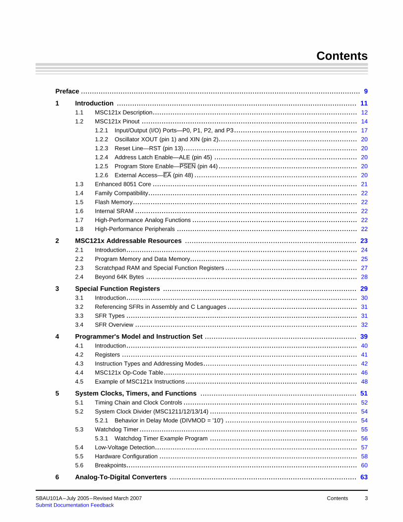
Contents
Preface ............................................................................................................................... 9
1 Introduction ............................................................................................................. 111.1 MSC121x Description............................................................................................. 12
1.2 MSC121x Pinout .................................................................................................. 14
1.2.1 Input/Output (I/O) Ports—P0, P1, P2, and P3........................................................ 17
1.2.2 Oscillator XOUT (pin 1) and XIN (pin 2)............................................................... 20
1.2.3 Reset Line—RST (pin 13)............................................................................... 20
1.2.4 Address Latch Enable—ALE (pin 45) ................................................................. 20
1.2.5 Program Store Enable—PSEN (pin 44) ............................................................... 20
1.2.6 External Access—EA (pin 48) .......................................................................... 20
1.3 Enhanced 8051 Core ............................................................................................. 21
1.4 Family Compatibility............................................................................................... 22
1.5 Flash Memory...................................................................................................... 22
1.6 Internal SRAM ..................................................................................................... 22
1.7 High-Performance Analog Functions ........................................................................... 22
1.8 High-Performance Peripherals .................................................................................. 22
2 MSC121x Addressable Resources .............................................................................. 232.1 Introduction......................................................................................................... 24
2.2 Program Memory and Data Memory............................................................................ 25
2.3 Scratchpad RAM and Special Function Registers ............................................................ 27
2.4 Beyond 64K Bytes ................................................................................................ 28
3 Special Function Registers ........................................................................................ 293.1 Introduction......................................................................................................... 30
3.2 Referencing SFRs in Assembly and C Languages ........................................................... 31
3.3 SFR Types ......................................................................................................... 31
3.4 SFR Overview ..................................................................................................... 32
4 Programmer's Model and Instruction Set ..................................................................... 394.1 Introduction......................................................................................................... 40
4.2 Registers ........................................................................................................... 41
4.3 Instruction Types and Addressing Modes...................................................................... 42
4.4 MSC121x Op-Code Table........................................................................................ 46
4.5 Example of MSC121x Instructions .............................................................................. 48
5 System Clocks, Timers, and Functions ....................................................................... 515.1 Timing Chain and Clock Controls ............................................................................... 52
5.2 System Clock Divider (MSC1211/12/13/14) ................................................................... 54
5.2.1 Behavior in Delay Mode (DIVMOD = '10') ............................................................ 54
5.3 Watchdog Timer ................................................................................................... 55
5.3.1 Watchdog Timer Example Program ................................................................... 56
5.4 Low-Voltage Detection............................................................................................ 57
5.5 Hardware Configuration .......................................................................................... 58
5.6 Breakpoints......................................................................................................... 60
6 Analog-To-Digital Converters ..................................................................................... 63
SBAU101A–July 2005–Revised March 2007 Contents 3Submit Documentation Feedback

6.1 ADC Functional Blocks ........................................................................................... 64
6.2 ADC Signal Flow and General Description .................................................................... 65
6.3 Analog Input Stage................................................................................................ 65
6.4 Input Impedance, PGA, and Voltage References............................................................. 67
6.5 Offset DAC ......................................................................................................... 69
6.6 ADC Data Rate, Filters, and Calibration ....................................................................... 70
6.7 32-Bit Summation Register ...................................................................................... 72
6.8 Accessing the ADC Multi-Byte Conversion in C .............................................................. 74
6.9 ADC Example Program........................................................................................... 75
7 Digital-To-Analog Converters ..................................................................................... 797.1 Introduction......................................................................................................... 80
7.2 DAC Selection ..................................................................................................... 81
7.3 DAC Configuration and Control ................................................................................. 83
7.4 DAC Technology and Limitations ............................................................................... 84
7.5 DAC Example Program........................................................................................... 84
8 Pulse-Width Modulator and Tone Generator ................................................................ 858.1 Description ......................................................................................................... 86
8.2 PWM Generator Example ........................................................................................ 87
9 Inter-IC (I2C™) Subsystem ......................................................................................... 899.1 Introduction to the I2C Bus ....................................................................................... 90
9.2 I2C Terminology ................................................................................................... 90
9.3 I2C Bus Lines and Basic Timing................................................................................. 91
9.4 I2C Data Transfers and the Acknowledge Bit.................................................................. 92
9.5 I2C Principal Registers............................................................................................ 93
9.6 I2C Related Registers............................................................................................. 96
9.7 I2C Example—MSC1211/13 as a Master ...................................................................... 97
9.8 I2C Example—MSC1211/13 as a Slave........................................................................ 99
9.9 I2C Example—MSC1211/13 as an Interrupt-Driven Slave ................................................. 100
9.10 I2C Synchronization and Arbitration ........................................................................... 101
9.11 I2C Fast Mode .................................................................................................... 101
9.12 I2C General Call.................................................................................................. 101
9.13 I2C 10-Bit Addressing ........................................................................................... 102
10 Serial Peripheral Interface (SPI™) ............................................................................. 10310.1 Description........................................................................................................ 104
10.2 SPI Configuration ................................................................................................ 104
10.3 SPI Interrupts..................................................................................................... 107
10.4 SPI FIFO Buffer .................................................................................................. 108
10.5 SPI Examples .................................................................................................... 111
11 Timers and Counters ............................................................................................... 11311.1 Description........................................................................................................ 114
11.2 Timer/Counters 0 and 1......................................................................................... 114
11.2.1 Modes 0 and 1 ......................................................................................... 116
11.2.2 Mode 2 .................................................................................................. 117
11.2.3 Mode 3 .................................................................................................. 117
11.2.4 Summary of Control Bits and SFRs for Timer/Counters 0 and 1................................ 118
11.3 Timer/Counter 2.................................................................................................. 119
11.3.1 16-Bit Timer/Counter with Optional Capture ....................................................... 120
4 Contents SBAU101A–July 2005–Revised March 2007Submit Documentation Feedback
11.3.2 16-Bit Timer/Counter with Automatic and Forced Reload........................................ 121
11.3.3 Baud Rate Generator ................................................................................. 122
11.3.4 Summary of Timer/Counter 2 Mode Control ....................................................... 123
11.3.5 Summary of Control Bits and SFRs for Timer/Counter 2......................................... 123
11.3.6 Summary of Timer Modes ............................................................................ 123
11.4 Example Program Using Timers 0, 1, and 2 ................................................................. 124
12 Serial Ports (USART0 and USART1) .......................................................................... 12512.1 Description........................................................................................................ 126
12.2 Control Bits in SCON0 and SCON1 ........................................................................... 126
12.3 Pin and Interrupt Assignments ................................................................................. 127
12.4 Timer/Counters 1 and 2 Baud Rate Generation ............................................................. 127
12.5 Mode 0—8-Bit Synchronous ................................................................................... 129
12.6 Mode 1—10-Bit Asynchronous................................................................................. 130
12.7 Modes 2 and 3—11-Bit Asynchronous........................................................................ 131
12.8 Multiprocessor Communications ............................................................................... 132
12.9 Example Program................................................................................................ 132
13 Interrupts ............................................................................................................... 13513.1 Description........................................................................................................ 136
13.2 Standard and Extended Interrupts............................................................................. 137
13.3 Auxiliary Interrupt Sources...................................................................................... 139
13.4 Multiple Interrupts................................................................................................ 140
13.5 Example of Multiple and Nested Interrupts................................................................... 140
13.6 Example of Wake Up from Idle ................................................................................ 143
Revision History ............................................................................................................... 145
SBAU101A–July 2005–Revised March 2007 Contents 5Submit Documentation Feedback
List of Figures
1-1 MSC121x Block Diagram.................................................................................................. 121-2 MSC121x Pin Configuration .............................................................................................. 141-3 Standard 8051 I/O Pin Structure ......................................................................................... 171-4 CMOS Output Pin Structure .............................................................................................. 171-5 Open-Drain Output Pin Structure ........................................................................................ 171-6 Input Pin Structure ......................................................................................................... 171-7 Comparison of MSC121x Timing to Standard 8051 Timing .......................................................... 212-1 On-Chip and Off-Chip Resources ........................................................................................ 242-2 Memory Map ................................................................................................................ 255-1 MSC121x Timing Chain and Clock Control............................................................................. 526-1 ADC Subsystem Elements ................................................................................................ 646-2 Input Multiplexer Configuration ........................................................................................... 666-3 Analog Input Structure without Buffer ................................................................................... 676-4 Filter Frequency Responses .............................................................................................. 717-1 DAC Architecture ........................................................................................................... 809-1 I2C Bus Connection of Standard and Fast Mode Devices ............................................................ 919-2 START and STOP Conditions ............................................................................................ 919-3 I2C-Bus Bit Transfer........................................................................................................ 919-4 I2C-Bus Data Transfer ..................................................................................................... 929-5 I2C Acknowledge ........................................................................................................... 9210-1 SPI Master/Slave Interconnect.......................................................................................... 10410-2 SPI Clock/Data Timing ................................................................................................... 10610-3 SPI FIFO Operation ...................................................................................................... 10811-1 Timer 0/1—Modes 0 and 1 .............................................................................................. 11611-2 Timer 0/1—Mode 2 ....................................................................................................... 11711-3 Timer 0—Mode 3 ......................................................................................................... 11711-4 Timer/Counter 2—16-Bit with Capture ................................................................................. 12011-5 Timer/Counter 2—16-Bit with Reload .................................................................................. 12111-6 Timer/Counter 2—Baud Rate Generator .............................................................................. 12212-1 Synchronous Receive at fCLK/4.......................................................................................... 12912-2 Synchronous Transmit at fCLK/4 ......................................................................................... 12912-3 Asynchronous 10-Bit Transmit Timing ................................................................................. 13012-4 Asynchronous 10-Bit Receive Timing .................................................................................. 13012-5 Asynchronous 11-Bit Receive........................................................................................... 13112-6 Asynchronous 11-Bit Transmit .......................................................................................... 13112-7 Serial Port with Software Buffer......................................................................................... 13213-1 Interrupts ................................................................................................................... 138
6 List of Figures SBAU101A–July 2005–Revised March 2007Submit Documentation Feedback
List of Tables
1-1 MSC121x Product Family Matrix ......................................................................................... 131-2 Pin Descriptions ............................................................................................................ 151-3 Port 1 Alternate Functions ................................................................................................ 181-4 Port 3 Alternate Functions ................................................................................................ 192-1 Program Memory and External Data Memory Addresses ............................................................ 252-2 MSC121x Flash Memory Partitioning and Addresses................................................................. 262-3 On-Chip 8051 Memory .................................................................................................... 273-1 Special Function Register Map ........................................................................................... 303-2 SFR Overview .............................................................................................................. 324-1 8051 Working Registers ................................................................................................... 414-2 Symbol Descriptions for Instruction List of Table 4-3.................................................................. 424-3 Instruction List .............................................................................................................. 434-4 MSC121x Op-Codes....................................................................................................... 465-1 SYSCLK—System Clock Divider Register.............................................................................. 545-2 Watchdog Control Bits..................................................................................................... 555-3 LVDCON—Low-Voltage Detect Control................................................................................. 575-4 Low-Voltage Detect ........................................................................................................ 575-5 HCR0—Hardware Configuration Register 0 ............................................................................ 585-6 HCR1—Hardware Configuration Register 1 ............................................................................ 595-7 MCON—Memory Control.................................................................................................. 605-8 BPCON—Breakpoint Control ............................................................................................. 605-9 BPL—Breakpoint Low Address for BP Register Selected in MCON at 95h........................................ 615-10 BPH—Breakpoint High Address for BP Register Selected in MCON at 95h....................................... 615-11 Breakpoints.................................................................................................................. 616-1 ADMUX—ADC Multiplexer................................................................................................ 666-2 Impedance Divisor (G) for a Given PGA ................................................................................ 676-3 ADCON0—ADC Control Register 0 ..................................................................................... 686-4 ADCON0 PGA Bit Parameters ........................................................................................... 686-5 ADCON1—ADC Control Register 1 ..................................................................................... 706-6 ADC Interrupt Controls .................................................................................................... 726-7 Summation Register ....................................................................................................... 726-8 SSCON—Summation/Shift Control ...................................................................................... 736-9 Summation Interrupt Controls ............................................................................................ 737-1 DACSEL Values ............................................................................................................ 817-2 LOADCON SFR ............................................................................................................ 817-3 DxLOAD Output Modes for DACx ....................................................................................... 817-4 DAC Control Registers .................................................................................................... 838-1 PWMCON—PWM Control ................................................................................................ 868-2 PWM Output ................................................................................................................ 879-1 I2C Terminology ............................................................................................................ 909-2 I2CCON—I2C Control Register .......................................................................................... 939-3 I2CDATA SFR .............................................................................................................. 949-4 I2CGM—I2C General Call / Multiple Master Control................................................................... 949-5 I2CSTAT SFR .............................................................................................................. 949-6 I2C Status Codes ........................................................................................................... 959-7 PDCON of I2C and SPI .................................................................................................... 969-8 Interrupt Control for I2C.................................................................................................... 969-9 Address Allocation ........................................................................................................ 10210-1 SPICON—SPI Control ................................................................................................... 105
SBAU101A–July 2005–Revised March 2007 List of Tables 7Submit Documentation Feedback
10-2 P1—Port 1 ................................................................................................................. 10510-3 P1DDRH—Port 1 Data Direction Register ............................................................................ 10510-4 SPIDATA—SPI Data Register .......................................................................................... 10610-5 SPI Interrupts Have Highest Priority and Jump to Address 0033h................................................. 10710-6 PAI—Pending Auxiliary Interrupt Register............................................................................. 10710-7 SPISTART—SPI Buffer Start Address................................................................................. 10910-8 SPISEND—SPI Buffer End Address ................................................................................... 10910-9 SPIRCON—SPI Receive Control Register ............................................................................ 11010-10 SPITCON—SPI Transmit Control Register............................................................................ 11011-1 TMOD—Timer Mode Control............................................................................................ 11411-2 TCON—Timer/Counter Control ......................................................................................... 11511-3 Modes 0 and 1 Operation................................................................................................ 11611-4 Control Bit and SFR Summary for Timer/Counters 0 and 1 ........................................................ 11811-5 T2CON—Timer 2 Control................................................................................................ 11911-6 Mode Control Summary for Timer/Counter 2 ......................................................................... 12311-7 Control Bit and SFR Summary for Timer/Counter 2 ................................................................. 12311-8 Timer Modes .............................................................................................................. 12312-1 SCON0 and SCON1—Serial Port 0 and Serial Port 1 Control ..................................................... 12612-2 USART Pin and Interrupt Assignments ................................................................................ 12712-3 Timer/Counter 2 Baud Rate Generation ............................................................................... 12712-4 Timer/Counter 1 Baud Rate Generation ............................................................................... 12712-5 USART Baud Rate Generation ......................................................................................... 12813-1 Standard and Extended Interrupts...................................................................................... 13713-2 Auxiliary Interrupts with Highest Group Priority....................................................................... 13913-3 EWU—Enable Wake Up ................................................................................................. 143
8 List of Tables SBAU101A–July 2005–Revised March 2007Submit Documentation Feedback

PrefaceSBAU101A–July 2005–Revised March 2007
About This Manual
This user's guide describes the function and operation of the MSC121x family of precision ADC and DACswith 8051 microcontroller and flash memory.
This document applies to the following MSC devices:
• MSC1210• MSC1211• MSC1212• MSC1213• MSC1214
For convenience, the abbreviation MSC121x is used to indicate all of the MSC devices listed in this user'sguide, unless otherwise specified.
Related Documentation and Tools From Texas Instruments
Data Sheets Literature Number
MSC1210 SBAS203
MSC1211 SBAS323
MSC1212 SBAS323
MSC1213 SBAS323
MSC1214 SBAS323
User's Guides Literature Number
MSC120x User Guide SBAU112
MSC1211EVM User’s Guide SBAU086
MSC1210EVM User’s Guide SBAU073
MSC1210-DAQ-EVM User’s Guide SBAU083
For a complete list of application notes and related documentation, see the MSC web site atwww.ti.com/msc.
SBAU101A–July 2005–Revised March 2007 9Submit Documentation Feedback
www.ti.com
Trademarks
Trademarks
I2C is a trademark of NXP Semiconductors.
SPI is a trademark of Motorola Inc.
All other trademarks are the property of their respective owners.
10 SBAU101A–July 2005–Revised March 2007Submit Documentation Feedback
Chapter 1SBAU101A–July 2005–Revised March 2007
Introduction
This chapter provides a functional overview of the MSC121x precision analog-to-digitalconverter (ADC) and digital-to-analog converters (DACs) with 8051 microcontroller andflash memory.
Topic .................................................................................................. Page
1.1 MSC121x Description ................................................................ 121.2 MSC121x Pinout........................................................................ 141.3 Enhanced 8051 Core ................................................................. 211.4 Family Compatibility.................................................................. 221.5 Flash Memory ........................................................................... 221.6 Internal SRAM........................................................................... 221.7 High-Performance Analog Functions........................................... 221.8 High-Performance Peripherals .................................................... 22
SBAU101A–July 2005–Revised March 2007 Introduction 11Submit Documentation Feedback

www.ti.com
1.1 MSC121x Description
ACC
MUX
AGND
+AVDD
AVDD
BUF PGA
VREF
Modulator
Up to 32KFLASH
1.2KSRAM
SPIFIFO
DigitalFilter
8051
SFR
SYS ClockDivider
LVD
BOR
POR
PORT1
PORT2
WDT
Timers/Counters
ClockGenerator
PORT0
PORT3
8
8
8
EA
8
T2SPI/EXT/I2C(4)
USART1
ADDR
ADDRDATA
AlternateFunctions
USART0EXTT0T1PWMRW
8−BitOffset DACIDAC0(3)/AIN0
IDAC1(3)/AIN1
VDAC2(3)/AIN2
VDAC3(3)/AIN3
AIN4
AIN5
AIN6
AIN7
AINCOM
AGND REFOUT/REF IN+(1) REF IN−(2) DVDD DGND
XIN XOUT
VDAC0
VDAC1
VDAC2
VDAC3
AIN2
AIN3
VDAC1(3)VDAC0(3)
ALE
PSEN
V/IConverter
V/IConverter
TemperatureSensor
RST
RDAC1(3)
IDAC0/AIN0
IDAC1/AIN1
RDAC0(3)
NOTES: (1) On the MSC1210, the REF IN + (pin 30) and REFOUT (pin 31) functions are split onto two pins. On the MSC1211/12/13/14,
REFOUT and REF IN+ are combined onto pin 30, and the VDAC1 output is on pin 31.
(2) REF IN− must be tied to AGND when using internal VREF.
(3) DAC functions are only available on the MSC1211/12/13/14.
(4) I2C is available only on the MSC1211 and MSC1213.
MSC121x Description
The MicroSystem family of devices is designed for high-resolution measurement applications in smarttransmitters, industrial process control, weigh scales, chromatography, and portable instrumentation. Theyprovide cost-effective, high-performance, mixed-signal solutions. The MicroSystem family not onlyincludes high-performance analog features and digital processing capability, but also integrates manydigital peripherals to offer a unique and effective system solution.
The main components of a MicroSystem product include:
• High-performance analog functions• Low-power enhanced 8051 microcontroller core• RAM and Flash memory• High-performance digital peripherals
The enhanced 8051 microcontroller includes dual data pointers and executes most instructions up to threetimes faster than a standard 8051 core. This increased execution speed provides greater flexibility inapplications requiring a trade-off among speed, power and noise. A block diagram is shown in Figure 1-1.
Figure 1-1. MSC121x Block Diagram
12 Introduction SBAU101A–July 2005–Revised March 2007Submit Documentation Feedback

www.ti.com
MSC121x Description
For some designers, the MSC121x is viewed as a microcontroller with integrated analog functions, whileto others it is a high-performance analog-to-digital converter (ADC) with an integrated microcontroller. TheMSC121x provides unparalleled analog and digital integration for all designers who are concerned withembedded instrumentation and control.
Complementing the high-resolution ADC are a precision voltage reference, programmable gain amplifier(PGA), and analog multiplexer (mux), as well as a temperature sensor and low voltage detectors.
Apart from numerous bit-wise programmable digital ports, there are two USARTs, three timer/counters, awatchdog timer, and a serial (SPI™) bus. Up to 32k of FLASH memory and 1.2K RAM are included aswell. The MSC1211/13 also support I2C serial transfers.
Taken together, the MSC121x features blend analog and digital functions to significantly simplify theoverall system design, which reduces the design time and board space as well as the need for externalcomponents.
For systems requiring additional memory, address and data lines are provided via multifunction I/O ports.
Table 1-1 compares the basic features and functionality of the MSC121x family.
Table 1-1. MSC121x Product Family MatrixMSC1210 MSC1211 MSC1212 MSC1213 MSC1214
Clock Frequency 33 33 33 33 33(kB)
Flash Memory 32 32 32 32 32(kB)
SRAM 1.2 1.2 1.2 1.2 1.2(kB)
ADC 8 × 24 8 × 24 8 × 24 8 × 24 8 × 24(Channel x Resolution)
DAC Quad Voltage / Dual Quad Voltage / Dual Dual Voltage / Dual Dual Voltage / DualN/A(Channel x Resolution) Current × 16 Current × 16 Current × 16 Current × 16
Features: 34 I/O 34 I/O 34 I/O 34 I/O 34 I/O32-Bit Accumulator External Memory External Memory External Memory External Memory External Memory
Internal VREF Dual USARTs Dual USARTs Dual USARTs Dual USARTs Dual USARTsInternal PGA - - -I2C I2C
Internal Buffer Serial/Parallel Serial/Parallel Serial/ParallelSerial/Parallel Serial/ParallelSPI Programming Programming ProgrammingProgramming Programming
Brownout Reset - System Clock Divider System Clock DividerSystem Clock Divider System Clock DividerLow-Voltage Detect
Package TQFP-64 TQFP-64 TQFP-64 TQFP-64 TQFP-64
SBAU101A–July 2005–Revised March 2007 Introduction 13Submit Documentation Feedback
www.ti.com
1.2 MSC121x Pinout
48
47
46
45
44
43
42
41
40
39
38
37
36
35
34
33
EA
P0.6/AD6
P0.7/AD7
ALE
PSEN/OSCCLK/MODCLK
P2.7/A15
DVDD
DGND
P2.6/A14
P2.5/A13
P2.4/A12
P2.3/A11
P2.2/A10
P2.1/A09
P2.0/A08
NC
1
2
3
4
5
6
7
8
9
10
11
12
13
14
15
16
XOUT
XIN
P3.0/RxD0
P3.1/TxD0
P3.2/INT0
P3.3/ /TONE/PWMINT1
P3.4/T0
P3.5/T1
P3.6/WR
P3.7/RD
DVDD
DGND
RST
DVDD
DVDD
RDAC0 or NC(2)
P1.7
//
/SC
KS
CL
INT
5(1
)
P1.6
/IN
T4/M
ISO
/SD
A(1
)
P1.5
//M
OS
IIN
T3
P1.4
/IN
T2/S
S
P1.3
/TxD
1
P1.2
/RxD
1
DV
DD
DG
ND
P1.1
/T2E
X
P1.0
/T2
P0.0
/AD
0
P0.1
/AD
1
P0.2
/AD
2
P0.3
/AD
3
P0.4
/AD
4
P0.5
/AD
5
VD
AC
0or
AG
ND
(3)
IDA
C0
/AIN
0(4
)
IDA
C1
/AIN
1(4
)
VD
AC
2/A
IN2
(5)
VD
AC
3/A
IN3
(5)
AIN
4
AIN
5
AIN
6/E
XT
D
AIN
7/E
XTA
AIN
CO
M
AG
ND
AV
DD
RE
F IN
-
RE
FO
UT
/RE
F IN
+(6
)
VD
AC
1or
RE
FO
UT
(6)
RD
AC
1or
NC
(2)
64 63 62 61 60 59 58 57 56 55 54
17 18 19 20 21 22 23 24 25 26 27
53 52 51 50 49
28 29 30 31 32
MSC121x
Non-bolded pin names are on MSC1210.
(1) SCL and SDA not present on MSC1210/12/14.
(2) Pins 16 and 32 are not connected (NC) on MSC1210.
(3) AGND for MSC1210; VDAC0 for MSC1211/12/13/14.
(4) IDAC0 and IDAC1 on MSC1211/12/13/14.
(5) VDAC2 and VDAC3 on MSC1211/12.
(6) For MSC1210, REFOUT is on pin 31. For MSC1211/12/13/14, REFOUT is shared with REF IN+ on pin 30, and VDAC1 is on pin 31.
NOTES:
MSC121x Pinout
The names and functions of pins are similar to those found on most 8051-compatible devices, but withextensions that are specific to the MSC121x. The pin configuration is shown in Figure 1-2, and the pindescriptions are listed in Table 1-2.
Figure 1-2. MSC121x Pin Configuration
14 Introduction SBAU101A–July 2005–Revised March 2007Submit Documentation Feedback
www.ti.com
MSC121x Pinout
Table 1-2. Pin DescriptionsPin # Name Description
1 XOUT The output of an oscillator that supports parallel resonant AT-cut crystals and ceramic resonators.
2 XIN The input to the crystal oscillator that can also be used as an external clock input.
3-10 P3.0-P3.7 Port 3 is an 8-bit bidirectional Input/Output port with alternate functions.
Port 3.x Alternate Name(s) Alternate Use
P3.0 RxD0 Serial port 0 input
P3.1 TxD0 Serial port 0 output
P3.2 INT0 External Interrupt 0
P3.3 INT1/TONE/PWM External interrupt 1/TONE/PWM output
P3.4 T0 Timer 0 input
P3.5 T1 Timer 1 input
P3.6 WR External data memory write strobe
P3.7 RD External data memory read strobe
11, 14, 15, 42, 58 DVDD Digital power supplies. All must be used.
12, 41, 57 DGND Digital grounds. All must be used.
13 RST A high on the reset input for two clock cycles resets the device.
Alternate or Additional inBase MSC1210 Pin Function MSC1211/12/13/14
16 NC No connection RDAC0 (MSC1211/12/13/14 only)
17 AGND Analog ground VDAC0 (MSC1211/12/13/14 only)
18 AIN0 Analog input channel 0 = AIN0 AIN0 and IDAC0 (MSC1211/12/13/14 only)
19 AIN1 Analog input channel 1 = AIN1 AIN1 and IDAC1 (MSC1211/12/13/14 only)
20 AIN2 Analog input channel 2 = AIN2 AIN2 and VDAC2 (MSC1211/12 only)
21 AIN3 Analog input channel 3 = AIN3 AIN3 and VDAC3 (MSC1211/12 only)
22 AIN4 Analog input channel 4 = AIN4 Same
23 AIN5 Analog input channel 5 = AIN5 Same
24 AIN6, EXTD Analog input channel 6 = AIN6 and digital low voltage Samedetect input
25 AIN7, EXTA Analog input channel 7 = AIN7 and analog low voltage Samedetect input
26 AINCOM Analog common for single-ended inputs Same
27 AGND Analog ground Same
28 AVDD Analog power supply Same
29 REF IN– Voltage reference negative input Same
30 REF IN + Voltage reference positive input REFOUT/REF IN+
31 REFOUT Voltage reference output VDAC1 (MSC1211/12/13/14 only)
32 NC No connection RDAC1 (MSC1211/12/13/14 only)
33 NC No connection Same
34-40, 43 P2.0-P2.7 Port 2 is an 8-bit bidirectional input/output port with alternate functions.
Port 2.x Alternate Name Alternate Use
P2.0 A8 Address bit 8
P2.1 A9 Address bit 9
P2.2 A10 Address bit 10
P2.3 A11 Address bit 11
P2.4 A12 Address bit 12
P2.5 A13 Address bit 13
P2.6 A14 Address bit 14
P2.8 A15 Address bit 15
SBAU101A–July 2005–Revised March 2007 Introduction 15Submit Documentation Feedback

www.ti.com
MSC121x Pinout
Table 1-2. Pin Descriptions (continued)Pin # Name Description
44 PSEN, OSCCLK, Program store enable. Connected to optional external memory as a chip enable. PSEN provides anMODCLK, Low or active low pulse. It is used in conjunction with RST and ALE to define serial or parallel programming
High mode. When not using external program memory, this pin can also be selected to output the oscillatorclock, ADC modulator clock, low or high. (See SFR PASEL, F2h.)
ALE PSEN Program Mode Selection (at reset)
NC NC Normal operation
0 1 Parallel programming of FLASH
1 0 Serial Programming of FLASH
0 0 Reserved
45 ALE, Low or High Address latch enable. Used for latching the low byte of the address during an access to externalmemory. (See PSEN and SFR PASEL, F2h.)
48 EA If EA is low as RST falls, and neither ALE nor PSEN is low (see above), code access will always be toexternal memory starting at address 0000h. Otherwise, internal program memory will be accessedwhere available.
46, 47, 49-54 P0.0-P0.7 Port 0 is an 8-bit bidirectional input/output port with alternate functions.
Port 0.x Alternate Name Alternate Use
P0.0 AD0 Address/Data bit 0
P0.1 AD1 Address/Data bit 1
P0.2 AD2 Address/Data bit 2
P0.3 AD3 Address/Data bit 3
P0.4 AD4 Address/Data bit 4
P0.5 AD5 Address/Data bit 5
P0.6 AD6 Address/Data bit 6
P0.7 AD7 Address/Data bit 7
55, 56, 59-64 P1.0-P1.7 Port 1 is an 8-bit bidirectional input/output port with alternate functions.
Port 1.x Alternate Name Alternate Use
P1.0 T2 Address/Data bit 0
P1.1 T2EX Address/Data bit 1
P1.2 RxD1 Address/Data bit 2
P1.3 TxD1 Address/Data bit 3
P1.4 INT2/SS Address/Data bit 4
P1.5 INT3/MOSI Address/Data bit 5
P1.6 INT4/MISO/SDA (1) Address/Data bit 6
P1.7 INT5/SCL (1)/SCK Address/Data bit 7(1) SCL and SDA not present on MSC1210/12/14.
Introduction16 SBAU101A–July 2005–Revised March 2007Submit Documentation Feedback
www.ti.com
1.2.1 Input/Output (I/O) Ports—P0, P1, P2, and P3
10kΩ
DVDD
Pn.n
Read Pin
Read Register
All Functions
Reg n.n
CMOS Output
Open−DrainOutput
Input
MSC121x Pinout
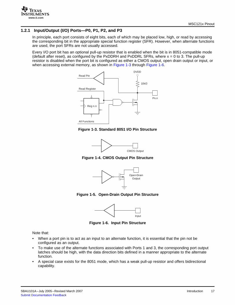
In principle, each port consists of eight bits, each of which may be placed low, high, or read by accessingthe corresponding bit in the appropriate special function register (SFR). However, when alternate functionsare used, the port SFRs are not usually accessed.
Every I/O port bit has an optional pull-up resistor that is enabled when the bit is in 8051-compatible mode(default after reset), as configured by the PxDDRH and PxDDRL SFRs, where x = 0 to 3. The pull-upresistor is disabled when the port bit is configured as either a CMOS output, open drain output or input, orwhen accessing external memory, as shown in Figure 1-3 through Figure 1-6.
Figure 1-3. Standard 8051 I/O Pin Structure
Figure 1-4. CMOS Output Pin Structure
Figure 1-5. Open-Drain Output Pin Structure
Figure 1-6. Input Pin Structure
Note that:
• When a port pin is to act as an input to an alternate function, it is essential that the pin not beconfigured as an output.
• To make use of the alternate functions associated with Ports 1 and 3, the corresponding port outputlatches should be high, with the data direction bits defined in a manner appropriate to the alternatefunction.
• A special case exists for the 8051 mode, which has a weak pull-up resistor and offers bidirectionalcapability.
SBAU101A–July 2005–Revised March 2007 Introduction 17Submit Documentation Feedback

www.ti.com
1.2.1.1 Port 0—P0
1.2.1.2 Port 1—P1
MSC121x Pinout
By default, Port 0 provides eight independently-programmable input/output bits. However, it may beconfigured to provide eight multiplexed, low-order address and data lines so that external memory may beaccessed. See bit 1 of hardware configuration register 1 (HCR1).
External memory cycles may occur if:
1. The EA pin is low when the RST pin is released;2. An instruction is fetched from an address that is not associated with on-chip FLASH; or3. When EGP0 (of HCR1) = 0 and a MOVC or MOVX instruction executes.
Port 1 provides not only eight independently-programmable bits, but also a variety of alternate functions,as shown in Table 1-3.
Table 1-3. Port 1 Alternate FunctionsPort 1 Bit Name Alternate Function
P1.0 (T2) Clock source for Timer/Counter 2 when C/T2 (T2CON.1) is 1.
If Timer/Counter 2 is in auto-reload mode and EXEN2 (T2CON.3) is 1, a negative edge (1–0 transition) causesP1.1 (T2EX) Timer/Counter 2 to be reloaded and EXF2 (T2CON.6) to be set, which in turn may cause an interrupt.
P1.2 (RxD1) Serial input to USART1. An external receiver is needed to level shift RS-232 signals.
P1.3 (TxD1) Serial output from USART1. An external driver is needed to level shift RS-232 signals.
P1.4 (INT2/SS) Positive-edge triggered external 2 interrupt or active-low Slave-Select output during SPI operations.
P1.5 (INT3/MOSI) Negative-edge triggered external 3 interrupt or the Master-Out/Slave-In during SPI operations.
P1.6 (INT4/MISO/SDA) Positive-edge triggered external 4 interrupt or Master-In/Slave-Out during SPI operation, serial data during I2C operation.
P1.7 (INT5/SCK/SCL) Negative-edge triggered external 5 interrupt or serial clock output for SPI operations, serial clock during I2C operation.
Introduction18 SBAU101A–July 2005–Revised March 2007Submit Documentation Feedback
www.ti.com
1.2.1.3 Port 2—P2
1.2.1.4 Port 3—P3
MSC121x Pinout
By default, Port 2 acts as eight general-purpose input/output signals. However, its alternate function is toprovide the upper byte of a 16-bit external address as determined by the EA pin and bit 0 (EGP23) ofHCR1. If EA is low when RST is de-asserted, all memory accesses are external, and Port 2 continuallyoutputs the high-order byte of 16-bit addresses. It also outputs bits of an address if EGP23 is 0 and aMOVX instruction is executed, regardless of EA. This is either the upper byte of the data pointer or thevalue in MPAGE at 92h, depending on whether the MOVX instruction references DPTR or @Rx,respectively.
When EA causes external memory accesses, the read and write strobes at P3.7 and P3.6, respectively,are enabled automatically. Selective external accesses must enable these strobes by clearing bit 1(EGP0) or bit 0 (EGP23) of HCR1 to 0.
If EGP23 = 1 and EA = 1, Port 2 output pins are always derived from its data latch.
Port 3 provides not olny eight independently programmable bits, but also a variety of alternate functions,as shown in Table 1-4.
Table 1-4. Port 3 Alternate FunctionsPort 3 Bit Name Alternate Function
P3.0 (RxD0) Serial input to USART0. An external receiver is needed for RS-232 signals.
P3.1 (TxD0) Serial output from USART0. An external driver is needed for RS-232 signals.
P3.2 (INT0) Active-low or negative-edge triggered interrupt. Gate for Timer/Counter 0.
P3.3 (INT1/TONE/PWM) Active-low or negative-edge triggered interrupt. Tone or Pulse-Width-Modulated output. Gate for Timer/Counter 1.
P3.4 (T0) Clock source for Timer/Counter 0 if TMOD.2 is 1. See description of the Timer/Counters for gated conditions.
P3.5 (IT1) Used as a clock source for Timer/Counter 1 if TMOD.6 is 1. See description of the Timer/Counters for gated conditions.
P3.6 (WR) Active-low write strobe for external memory if used.
P3.7 (RD) Active-low read strobe for external memory if used.
SBAU101A–July 2005–Revised March 2007 Introduction 19Submit Documentation Feedback
www.ti.com
1.2.2 Oscillator XOUT (pin 1) and XIN (pin 2)
1.2.3 Reset Line—RST (pin 13)
1.2.4 Address Latch Enable—ALE (pin 45)
1.2.5 Program Store Enable—PSEN (pin 44)
1.2.6 External Access—EA (pin 48)
MSC121x Pinout
In many applications, a quartz crystal or ceramic resonator is connected between XOUT and XIN toprovide a reference clock that is between 1MHz and approximately 30MHz. The static design of theMSC121x allows a digital clock to be applied to XIN that is between 0MHz and 30MHz. A commonly-usedcrystal for exact baud rates is 11.0592MHz.
Note: The load capacitors for the crystal must be verified to work over the operating conditionsof the application. It is generally better to use lower value load capacitors than thoserecommended by the crystal manufacturer because of the design of the oscillator circuit.
RST is the master reset line. When it is brought high for two or more clock cycles, the MSC121x is reset.All SFRs are placed at their default values and the program counter is reset to 0000h. The contents ofinternal SRAM are not affected by a reset, and instruction execution begins when RST is brought low,when both PSEN and ALE are high. If either PSEN or ALE is low when RST is brought low, the MSC121xenters Flash Programming mode.
The RST pin has a CMOS Schmitt-trigger input that permits the use of a simple RC network to achievereset when power is first applied. For the MSC1210, the internal pull-down resistor is typically 200kΩ. Forthe MSC1211/12/13/14, there is no internal pull-down resistor.
As RST is de-asserted (low), ALE temporarily acts as an input with a 9kΩ internal pull-up resistor and isused in conjunction with PSEN to place the MSC121x in a programming mode. If neither ALE nor PSENare pulled low, the MSC121x begins normal operation, where ALE is always an output that usuallycontrols a strobed latch to demultiplex the address appearing on Port 0.
When no external memory is present, ALE may be used as an independent output that can be placed lowor high via the ALE mode bits in PASEL at F2h.
As RST is de-asserted (low), PSEN temporarily acts as an input with a 9kΩ internal pull-up resistor, and isused in conjunction with ALE to place the MSC121x in a programming mode. If neither ALE nor PSEN arepulled low, the MSC121x begins normal operation, where PSEN is always an output that usually acts asan active-low strobe to read from external program memory.
When no external memory is present, PSEN may be used as an independent output that can be placedlow, high, or reflect the ADC modulator clock, via PSEN mode bits in PASEL at F2h.
EA is sampled as the RST pin is de-asserted (low) and determines whether the MSC121x fetchesinstruction codes from internal or external memory. When EA is high, code is fetched from internalmemory; otherwise, code is always fetched from external memory. Changing the level on EA duringnormal operation has no effect.
Code is fetched at addresses pointed to by the Program Counter (PC) during program execution and alsowhen a MOVC instruction is executed. In either case, if EA is high but there is no internal memoryassociated with a particular address, an external fetch will occur.
Introduction20 SBAU101A–July 2005–Revised March 2007Submit Documentation Feedback
www.ti.com
1.3 Enhanced 8051 Core
ALE
PSEN
AD0−AD7
PORT 2
ALE
PSEN
AD0−AD7
PORT 2
CLK
Sta
nd
ard
8051
Tim
ing
MS
C12
1xTi
min
g
Single−Byte, Single−CycleInstruction
Single−Byte, Single−CycleInstruction
12 Cycles
4 Cycles
Enhanced 8051 Core
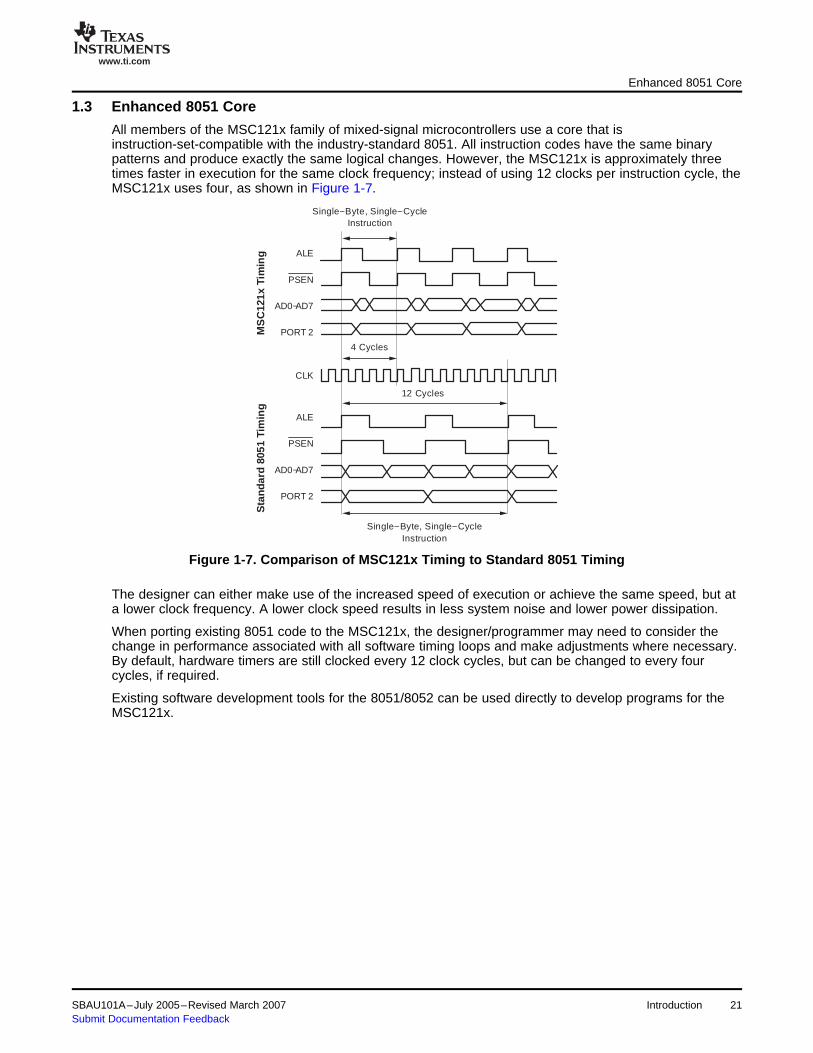
All members of the MSC121x family of mixed-signal microcontrollers use a core that isinstruction-set-compatible with the industry-standard 8051. All instruction codes have the same binarypatterns and produce exactly the same logical changes. However, the MSC121x is approximately threetimes faster in execution for the same clock frequency; instead of using 12 clocks per instruction cycle, theMSC121x uses four, as shown in Figure 1-7.
Figure 1-7. Comparison of MSC121x Timing to Standard 8051 Timing
The designer can either make use of the increased speed of execution or achieve the same speed, but ata lower clock frequency. A lower clock speed results in less system noise and lower power dissipation.
When porting existing 8051 code to the MSC121x, the designer/programmer may need to consider thechange in performance associated with all software timing loops and make adjustments where necessary.By default, hardware timers are still clocked every 12 clock cycles, but can be changed to every fourcycles, if required.
Existing software development tools for the 8051/8052 can be used directly to develop programs for theMSC121x.
SBAU101A–July 2005–Revised March 2007 Introduction 21Submit Documentation Feedback

www.ti.com
1.4 Family Compatibility
1.5 Flash Memory
1.6 Internal SRAM
1.7 High-Performance Analog Functions
1.8 High-Performance Peripherals
Family Compatibility
The MSC121x family allows the most cost-effective part to be used for each application and ensures amigration path towards larger memories when required. Code written for the 4K byte part runs unalteredon 8K, 16K, and 32K parts. Between the MSC1210 and MSC1211, the allocation and meaning of pins aresimilar, but not identical because of the different functions that are provided.
The MSC121x parts feature flexible Flash memory that can be partitioned into program and data areasthat are best suited for each application. They may be programmed over the entire operating voltagerange and temperature range using serial, parallel, and self-programming methodologies.
The MSC121x contains a total of 1280 bytes of static random access memory (SRAM). 128 bytes aredirectly addressable using instructions that incorporate the address. An additional 128 bytes are indirectlyaddressable via instructions using a register as a pointer, while 1024 bytes are logically external butphysically internal and accessed with the MOVX instruction.
The analog functionality of the MSC121x is state-of-the-art. The ADC is extremely low-noise, and meetsthe most stringent requirements for analog instrumentation. The integrated programmable gain amplifier(PGA) further improves the performance of the ADC, which then achieves nanovolt resolution.
The integrated low-drift, high-accuracy voltage reference complements the performance of the ADC andusually eliminates the need for an external reference. However, ratiometric measurements are stillpossible and easily implemented.
Also present are a programmable filter, an analog multiplexer for single-ended and differential signals, atemperature sensor, burnout current sources, an analog input buffer, and an offset DAC.
Additional digital peripherals are included, which offload CPU processing and control functions from thecore to improve further the overall efficiency. In particular, there is a 32-bit accumulator closely associatedwith the ADC, an SPI-compatible serial port with a FIFO buffer, two USARTs, power-on reset, brownoutreset, low-voltage detection, multiple digital ports with configurable I/O, a 16-bit pulse-width modulator(PWM), a watchdog timer, and three timer/counters.
The SPI interface and FIFO buffer allow synchronous serial communications with minimal CPU overhead.For the MSC1211 and MSC1213, an I2C interface may be enabled, which replaces the SPI.
The 32-bit accumulator significantly reduces the processing overhead associated with multi-byte data. Itallows automatic 32-bit additions from the ADC, and shifts without using CPU registers. 32-bit addition issupported with minimal program interaction.
22 Introduction SBAU101A–July 2005–Revised March 2007Submit Documentation Feedback
Chapter 2SBAU101A–July 2005–Revised March 2007
MSC121x Addressable Resources
This chapter provides a detailed description of the MSC121x addressable resources.
Topic .................................................................................................. Page
2.1 Introduction.............................................................................. 242.2 Program Memory and Data Memory ............................................ 252.3 Scratchpad RAM and Special Function Registers ......................... 272.4 Beyond 64K Bytes..................................................................... 28
SBAU101A–July 2005–Revised March 2007 MSC121x Addressable Resources 23Submit Documentation Feedback

www.ti.com
2.1 Introduction
64K bytesaddressable
ProgramSpace
On-chipFLASH,
ROM, RAMand/or
externalmemory
128 bytes
directly
addressable
RAM
128 bytes
indirectly
addressable
RAM
128 bytes
directly
addressable
SFRs
FFFF
0000
FF
00
80
7F
On-Chip Resources On-Chip and Off-Chip Resources
64K bytesaddressable
‘External’Data Space
On-chipFLASH,
RAMand/or
externalmemory
Introduction
Some microprocessors have a single unified address space that is used for program code, data valuesand input/output ports. However, most 8051 cores (and thus the MSC121x), have several distinctaddressable spaces that serve different purposes, as shown in Figure 2-1. In fact, the MSC121ximplements all address spaces found in the 8051, but with a feature that permits self-modifiable code.
Direct and indirect 8-bit addresses access up to 384 bytes of on-chip resources, comprised of 256 bytes ofstatic random access memory (SRAM) and up to 128 SFRs. 16-bit pointers (PC and DPTR) allow up to64K bytes of program memory and 64K bytes of extended data memory to be accessed, which may beon-chip and/or off-chip.
Memory for data may be allocated in different places, depending upon the size of the data, how frequentlyit is altered, and how efficiently it is accessed. The resources available on the MSC121x are:
• 256 bytes of on-chip SRAM for working registers, bit-wide variables, byte and multi-byte variables, anda stack. This memory is accessed by the majority of data-processing instructions.
• 1024 bytes of on-chip extended SRAM, which is considered by the architecture as logically externaldata. It is used for variables that are needed less frequently and accessed only with MOVX (X forexternal) instructions, even though it is on-chip.
• A configurable number of kilobytes of on-chip FLASH memory that is accessed only with MOVX (X forexternal) instructions, even though it is on-chip. Typically, data here consist of lookup tables.
• A configurable number of kilobytes of user-defined, read-only memory (ROM) that is off-chip. It isaccessed only with MOVX instructions.
Figure 2-1. On-Chip and Off-Chip Resources
Memory for program code may be on-chip or off-chip. On-chip, it is realized by FLASH, ROM, or SRAMwithin the address range of 0000 to FFFFh. During program execution, if a code address is referencedthat is not associated with on-chip memory, off-chip memory will be accessed. Even if on-chip programmemory is present, off-chip memory will be used, as long as EA is low when the RST (reset) pin isreleased. EA also overrides access to on-chip SRAM that is mapped into code space.
Both program memory and data memory have 16-bit address spaces. They are logically distinct andusually physically separate.
MSC121x Addressable Resources24 SBAU101A–July 2005–Revised March 2007Submit Documentation Feedback
www.ti.com
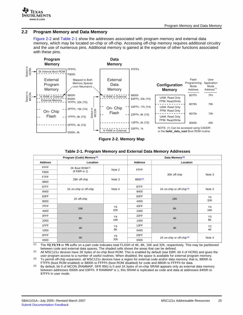
2.2 Program Memory and Data Memory
1k RAM or External1k RAM or External
1k RAM or External
External Memory
Sele
ct in
HC
R0
0000h, 0k
1FFFh, 8k (Y3)
0FFFh, 4k (Y2)
3FFFh, 16k (Y4)
8400h
7FFFh, 32k (Y5)
2k Internal Boot ROMF800h
FFFFh
External
Program
Memory
Mapped to Both
Memory Spaces
(von Neumann)
8800h
03FFh, 1k
13FFh, 5k (Y2)
23FFh, 9k (Y3)
43FFh, 17k (Y4)
83FFh, 33k (Y5)
FFFFh
External
Data
Memory
ProgramMemory
DataMemory
8800h
On- Chip
Flash
On- Chip
Flash
Flash
Programming
Mode
Address
User
Application
Mode
Address(1)
NOTE: (1) Can be accessed using CADDR
or the Boot ROM routine.faddr_data_read
UAM: Read Only
FPM: Read Only
UAM: Read Only
FPM: Read/Write
UAM: Read Only
FPM: Read/Write
807Fh
8000h
8070h
7Fh
8079h 79h
00h
70h
ConfigurationMemory
Sele
ct in
MC
ON
Sele
ct in
MC
ON
Program Memory and Data Memory
Figure 2-2 and Table 2-1 show the addresses associated with program memory and external datamemory, which may be located on-chip or off-chip. Accessing off-chip memory requires additional circuitryand the use of numerous pins. Additional memory is gained at the expense of other functions associatedwith these pins.
Figure 2-2. Memory Map
Table 2-1. Program Memory and External Data Memory AddressesProgram (Code) Memory (1) Data Memory (1)
Address Location Address Location
FFFF 2K Boot ROM (2)Note 2 FFFF(if EBR is 1)F800
30K off-chip Note 3F7FF
28K off-chip Note 3 8800 (3)
8800
87FF 87FF1K on-chip or off-chip Note 4 1K on-chip or off-chip (4) Note 4
8400 8400
83FF 83FF Y51K off-chip 16K 32K8000 4400
7FFF 43FFY5 Y416K 8K32K 16K4000 2400
3FFF 23FFY4 Y38K 4K16K 8K2000 1400
1FFF 13FFY3 Y24K 4K8K 4K1000 0400
0FFF 03FFY54K 1K on-chip or off-chip (4) Note 432k0000 0000(1) The Y2,Y3,Y4 or Y5 suffix on a part code indicates total FLASH of 4K, 8K, 16K and 32K, respectively. This may be partitioned
between code and external data spaces, The shaded cells shows the areas that can be defined.(2) All MSC121x devices have 2K bytes of on-chip Boot ROM. This is enabled by default (see EBR, bit 4 of HCR0) and gives the
user program access to a number of useful routines. When disabled, the space is available for external program memory.(3) To permit off-chip expansion, all MSC121x devices have a region for external code and/or data memory; that is, 8800h to
F7FFh (boot ROM enabled) or 8800h to FFFFh (boot ROM disabled) for code and 8800h to FFFFh for data.(4) By default, bit 0 of MCON (RAMMAP, SFR 95h) is 0 and 1K bytes of on-chip SRAM appears only as external data memory
between addresses 0000h and 03FFh. If RAMMAP is 1, this SRAM is replicated as code and data at addresses 8400h to87FFh in user mode.
SBAU101A–July 2005–Revised March 2007 MSC121x Addressable Resources 25Submit Documentation Feedback
www.ti.com
Program Memory and Data Memory
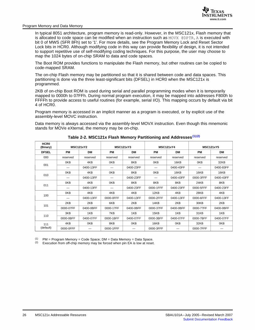
In typical 8051 architecture, program memory is read-only. However, in the MSC121x, Flash memory thatis allocated to code space can be modified when an instruction such as MOVX @DPTR,A is executed withbit 0 of MWS (SFR 8Fh) set to '1'. For more details, see the Program Memory Lock and Reset SectorLock bits in HCR0. Although modifying code in this way can provide flexibility of design, it is not intendedto support repetitive use of self-modifying coding techniques. For this purpose, the user may choose tomap the 1024 bytes of on-chip SRAM to data and code spaces.
The Boot ROM provides functions to manipulate the Flash memory, but other routines can be copied tocode-mapped SRAM.
The on-chip Flash memory may be partitioned so that it is shared between code and data spaces. Thispartitioning is done via the three least-significant bits (DFSEL) in HCR0 when the MSC121x isprogrammed.
2KB of on-chip Boot ROM is used during serial and parallel programming modes when it is temporarilymapped to 0000h to 07FFh. During normal program execution, it may be mapped into addresses F800h toFFFFh to provide access to useful routines (for example, serial I/O). This mapping occurs by default via bit4 of HCR0.
Program memory is accessed in an implicit manner as a program is executed, or by explicit use of theassembly-level MOVC instruction.
Data memory is always accessed via the assembly-level MOVX instruction. Even though this mnemonicstands for MOVe eXternal, the memory may be on-chip.
Table 2-2. MSC121x Flash Memory Partitioning and Addresses (1) (2)
HCR0(Binary) MSC121xY2 MSC121xY3 MSC121xY4 MSC121xY5
DFSEL PM DM PM DM PM DM PM DM
000 reserved reserved reserved reserved reserved reserved reserved reserved
0KB 4KB 0KB 8KB 0KB 16KB 0KB 32KB001
— 0400-13FF — 0400-23FF — 0400-43FF — 0400-83FF
0KB 4KB 0KB 8KB 0KB 16KB 16KB 16KB010
— 0400-13FF — 0400-23FF — 0400-43FF 0000-3FFF 0400-43FF
0KB 4KB 0KB 8KB 8KB 8KB 24KB 8KB011
— 0400-13FF — 0400-23FF 0000-1FFF 0400-23FF 0000-5FFF 0400-23FF
0KB 4KB 4KB 4KB 12KB 4KB 28KB 4KB100
— 0400-13FF 0000-0FFF 0400-13FF 0000-2FFF 0400-13FF 0000-6FFF 0400-13FF
2KB 2KB 6KB 2KB 14KB 2KB 30KB 2KB101
0000-07FF 0400-0BFF 0000-17FF 0400-0BFF 0000-37FF 0400-0BFF 0000-77FF 0400-0BFF
3KB 1KB 7KB 1KB 15KB 1KB 31KB 1KB110
0000-0BFF 0400-07FF 0000-1BFF 0400-07FF 0000-3BFF 0400-07FF 0000-7BFF 0400-07FF
4KB 0KB 8KB 0KB 16KB 0KB 32KB 0KB111(default) 0000-0FFF — 0000-1FFF — 0000-3FFF — 0000-7FFF —
(1) PM = Program Memory = Code Space; DM = Data Memory = Data Space.(2) Execution from off-chip memory may be forced when pin EA is low at reset.
MSC121x Addressable Resources26 SBAU101A–July 2005–Revised March 2007Submit Documentation Feedback
www.ti.com
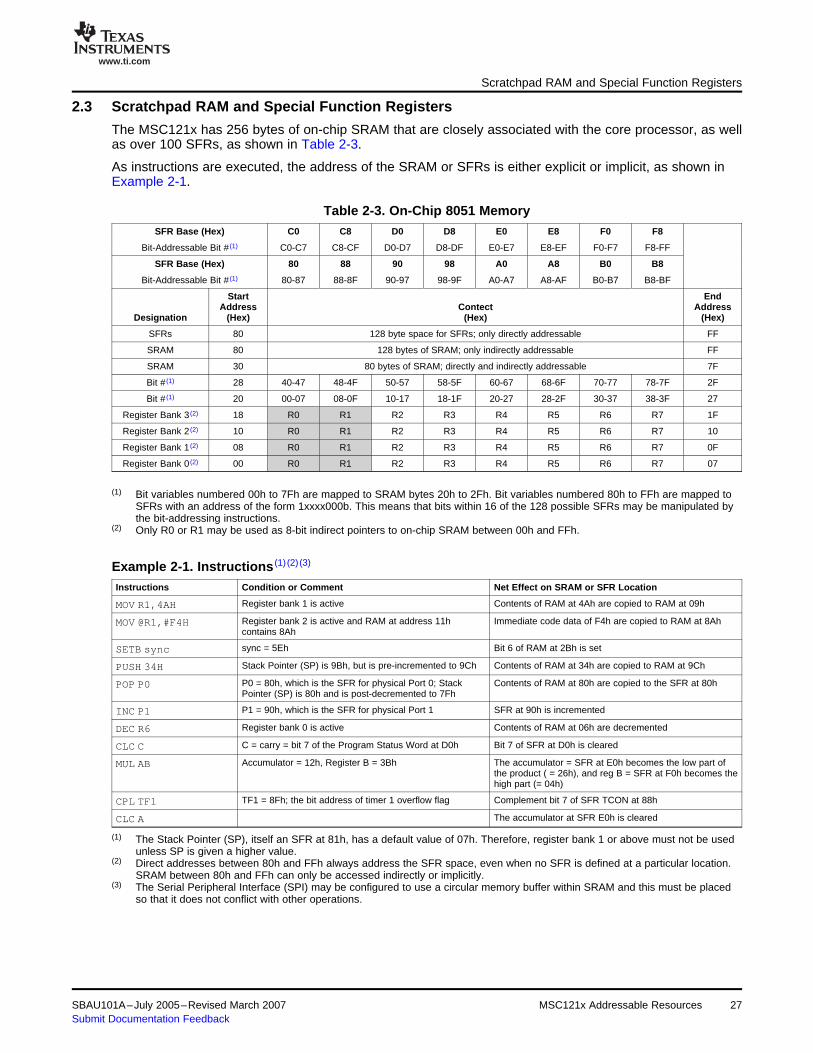
2.3 Scratchpad RAM and Special Function Registers
Scratchpad RAM and Special Function Registers
The MSC121x has 256 bytes of on-chip SRAM that are closely associated with the core processor, as wellas over 100 SFRs, as shown in Table 2-3.
As instructions are executed, the address of the SRAM or SFRs is either explicit or implicit, as shown inExample 2-1.
Table 2-3. On-Chip 8051 MemorySFR Base (Hex) C0 C8 D0 D8 E0 E8 F0 F8
Bit-Addressable Bit # (1) C0-C7 C8-CF D0-D7 D8-DF E0-E7 E8-EF F0-F7 F8-FF
SFR Base (Hex) 80 88 90 98 A0 A8 B0 B8
Bit-Addressable Bit # (1) 80-87 88-8F 90-97 98-9F A0-A7 A8-AF B0-B7 B8-BF
Start EndAddress Contect Address
Designation (Hex) (Hex) (Hex)
SFRs 80 128 byte space for SFRs; only directly addressable FF
SRAM 80 128 bytes of SRAM; only indirectly addressable FF
SRAM 30 80 bytes of SRAM; directly and indirectly addressable 7F
Bit # (1) 28 40-47 48-4F 50-57 58-5F 60-67 68-6F 70-77 78-7F 2F
Bit # (1) 20 00-07 08-0F 10-17 18-1F 20-27 28-2F 30-37 38-3F 27
Register Bank 3 (2) 18 R0 R1 R2 R3 R4 R5 R6 R7 1F
Register Bank 2 (2) 10 R0 R1 R2 R3 R4 R5 R6 R7 10
Register Bank 1 (2) 08 R0 R1 R2 R3 R4 R5 R6 R7 0F
Register Bank 0 (2) 00 R0 R1 R2 R3 R4 R5 R6 R7 07
(1) Bit variables numbered 00h to 7Fh are mapped to SRAM bytes 20h to 2Fh. Bit variables numbered 80h to FFh are mapped toSFRs with an address of the form 1xxxx000b. This means that bits within 16 of the 128 possible SFRs may be manipulated bythe bit-addressing instructions.
(2) Only R0 or R1 may be used as 8-bit indirect pointers to on-chip SRAM between 00h and FFh.
Example 2-1. Instructions (1) (2) (3)
Instructions Condition or Comment Net Effect on SRAM or SFR Location
Register bank 1 is active Contents of RAM at 4Ah are copied to RAM at 09hMOV R1,4AH
Register bank 2 is active and RAM at address 11h Immediate code data of F4h are copied to RAM at 8AhMOV @R1,#F4Hcontains 8Ah
sync = 5Eh Bit 6 of RAM at 2Bh is setSETB sync
Stack Pointer (SP) is 9Bh, but is pre-incremented to 9Ch Contents of RAM at 34h are copied to RAM at 9ChPUSH 34H
P0 = 80h, which is the SFR for physical Port 0; Stack Contents of RAM at 80h are copied to the SFR at 80hPOP P0Pointer (SP) is 80h and is post-decremented to 7Fh
P1 = 90h, which is the SFR for physical Port 1 SFR at 90h is incrementedINC P1
Register bank 0 is active Contents of RAM at 06h are decrementedDEC R6
C = carry = bit 7 of the Program Status Word at D0h Bit 7 of SFR at D0h is clearedCLC C
Accumulator = 12h, Register B = 3Bh The accumulator = SFR at E0h becomes the low part ofMUL ABthe product ( = 26h), and reg B = SFR at F0h becomes thehigh part (= 04h)
TF1 = 8Fh; the bit address of timer 1 overflow flag Complement bit 7 of SFR TCON at 88hCPL TF1
The accumulator at SFR E0h is clearedCLC A
(1) The Stack Pointer (SP), itself an SFR at 81h, has a default value of 07h. Therefore, register bank 1 or above must not be usedunless SP is given a higher value.
(2) Direct addresses between 80h and FFh always address the SFR space, even when no SFR is defined at a particular location.SRAM between 80h and FFh can only be accessed indirectly or implicitly.
(3) The Serial Peripheral Interface (SPI) may be configured to use a circular memory buffer within SRAM and this must be placedso that it does not conflict with other operations.
SBAU101A–July 2005–Revised March 2007 MSC121x Addressable Resources 27Submit Documentation Feedback

www.ti.com
2.4 Beyond 64K Bytes
Beyond 64K Bytes
If more than 64K bytes of either program or data storage are required, various bank switching techniquescan be used. These techniques may be supported automatically with some C compilers and developmentenvironments; refer to the particular software vendor for further information.
28 MSC121x Addressable Resources SBAU101A–July 2005–Revised March 2007Submit Documentation Feedback

Chapter 3SBAU101A–July 2005–Revised March 2007
Special Function Registers
This chapter describes the special function registers of the MSC121x.
Topic .................................................................................................. Page
3.1 Introduction.............................................................................. 303.2 Referencing SFRs in Assembly and C Languages......................... 313.3 SFR Types................................................................................ 313.4 SFR Overview ........................................................................... 32
SBAU101A–July 2005–Revised March 2007 Special Function Registers 29Submit Documentation Feedback
www.ti.com
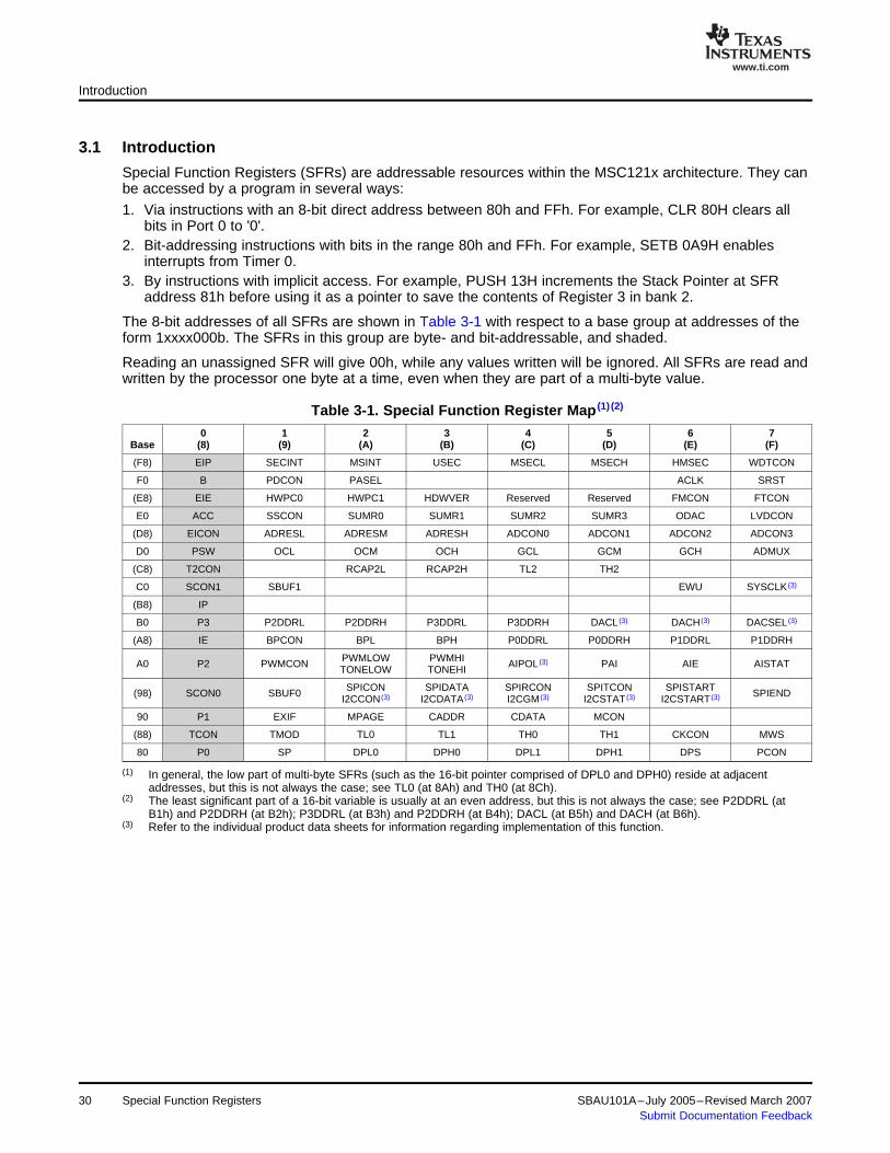
3.1 Introduction
Introduction
Special Function Registers (SFRs) are addressable resources within the MSC121x architecture. They canbe accessed by a program in several ways:
1. Via instructions with an 8-bit direct address between 80h and FFh. For example, CLR 80H clears allbits in Port 0 to '0'.
2. Bit-addressing instructions with bits in the range 80h and FFh. For example, SETB 0A9H enablesinterrupts from Timer 0.
3. By instructions with implicit access. For example, PUSH 13H increments the Stack Pointer at SFRaddress 81h before using it as a pointer to save the contents of Register 3 in bank 2.
The 8-bit addresses of all SFRs are shown in Table 3-1 with respect to a base group at addresses of theform 1xxxx000b. The SFRs in this group are byte- and bit-addressable, and shaded.
Reading an unassigned SFR will give 00h, while any values written will be ignored. All SFRs are read andwritten by the processor one byte at a time, even when they are part of a multi-byte value.
Table 3-1. Special Function Register Map (1) (2)
0 1 2 3 4 5 6 7Base (8) (9) (A) (B) (C) (D) (E) (F)
(F8) EIP SECINT MSINT USEC MSECL MSECH HMSEC WDTCON
F0 B PDCON PASEL ACLK SRST
(E8) EIE HWPC0 HWPC1 HDWVER Reserved Reserved FMCON FTCON
E0 ACC SSCON SUMR0 SUMR1 SUMR2 SUMR3 ODAC LVDCON
(D8) EICON ADRESL ADRESM ADRESH ADCON0 ADCON1 ADCON2 ADCON3
D0 PSW OCL OCM OCH GCL GCM GCH ADMUX
(C8) T2CON RCAP2L RCAP2H TL2 TH2
C0 SCON1 SBUF1 EWU SYSCLK (3)
(B8) IP
B0 P3 P2DDRL P2DDRH P3DDRL P3DDRH DACL (3) DACH (3) DACSEL (3)
(A8) IE BPCON BPL BPH P0DDRL P0DDRH P1DDRL P1DDRH
PWMLOW PWMHIA0 P2 PWMCON AIPOL (3) PAI AIE AISTATTONELOW TONEHI
SPICON SPIDATA SPIRCON SPITCON SPISTART(98) SCON0 SBUF0 SPIENDI2CCON (3) I2CDATA (3) I2CGM (3) I2CSTAT (3) I2CSTART (3)
90 P1 EXIF MPAGE CADDR CDATA MCON
(88) TCON TMOD TL0 TL1 TH0 TH1 CKCON MWS
80 P0 SP DPL0 DPH0 DPL1 DPH1 DPS PCON
(1) In general, the low part of multi-byte SFRs (such as the 16-bit pointer comprised of DPL0 and DPH0) reside at adjacentaddresses, but this is not always the case; see TL0 (at 8Ah) and TH0 (at 8Ch).
(2) The least significant part of a 16-bit variable is usually at an even address, but this is not always the case; see P2DDRL (atB1h) and P2DDRH (at B2h); P3DDRL (at B3h) and P2DDRH (at B4h); DACL (at B5h) and DACH (at B6h).
(3) Refer to the individual product data sheets for information regarding implementation of this function.
Special Function Registers30 SBAU101A–July 2005–Revised March 2007Submit Documentation Feedback
www.ti.com
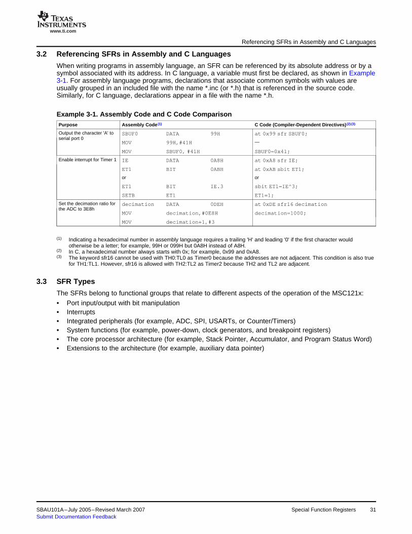
3.2 Referencing SFRs in Assembly and C Languages
3.3 SFR Types
Referencing SFRs in Assembly and C Languages
When writing programs in assembly language, an SFR can be referenced by its absolute address or by asymbol associated with its address. In C language, a variable must first be declared, as shown in Example3-1. For assembly language programs, declarations that associate common symbols with values areusually grouped in an included file with the name *.inc (or *.h) that is referenced in the source code.Similarly, for C language, declarations appear in a file with the name *.h.
Example 3-1. Assembly Code and C Code ComparisonPurpose Assembly Code (1) C Code (Compiler-Dependent Directives) (2) (3)
Output the character 'A' to SBUF0 DATA 99H at 0x99 sfr SBUF0;serial port 0
—MOV 99H,#41H
MOV SBUF0, #41H SBUF0=0x41;
Enable interrupt for Timer 1 IE DATA 0A8H at 0xA8 sfr IE;
ET1 BIT 0ABH at 0xAB sbit ET1;
or or
ET1 BIT IE.3 sbit ET1=IE^3;
SETB ET1 ET1=1;
Set the decimation ratio for decimation DATA 0DEH at 0xDE sfr16 decimationthe ADC to 3E8h
MOV decimation,#0E8H decimation=1000;
MOV decimation+1,#3
(1) Indicating a hexadecimal number in assembly language requires a trailing 'H' and leading '0' if the first character wouldotherwise be a letter; for example, 99H or 099H but 0A8H instead of A8H.
(2) In C, a hexadecimal number always starts with 0x; for example, 0x99 and 0xA8.(3) The keyword sfr16 cannot be used with TH0:TL0 as Timer0 because the addresses are not adjacent. This condition is also true
for TH1:TL1. However, sfr16 is allowed with TH2:TL2 as Timer2 because TH2 and TL2 are adjacent.
The SFRs belong to functional groups that relate to different aspects of the operation of the MSC121x:
• Port input/output with bit manipulation• Interrupts• Integrated peripherals (for example, ADC, SPI, USARTs, or Counter/Timers)• System functions (for example, power-down, clock generators, and breakpoint registers)• The core processor architecture (for example, Stack Pointer, Accumulator, and Program Status Word)• Extensions to the architecture (for example, auxiliary data pointer)
SBAU101A–July 2005–Revised March 2007 Special Function Registers 31Submit Documentation Feedback

www.ti.com
3.4 SFR OverviewSFR Overview
Table 3-2 lists the SFRs, with addresses and descriptions. Bold SFR names may not be available in allMSC121x devices. Shaded SFR addresses in the table are bit-addressable.
Table 3-2. SFR OverviewName Address (Hex) Description
P0 80h Port 0Controls the byte-wide, bit-programmable input/output called Port 0. Each bit in the SFRcorresponds to a pin on the actual part. Individual bits may be configured as bidirectional, CMOSoutput, open drain output, or input via the Data Direction SFRs for Port 0. See P0DDRL at ACh,and P0DDRH at ADh.The same device pins may also be used to provide a multiplexed address and data bus for accessto off-chip memory. In this case, bit 1 (EGP0) of HCR1 must be 0 and the program does notreference P0.
SP 81h Stack PointerSP acts as an 8-bit pointer to core RAM. It creates a last-in/first-out data structure that is used bythe instructions PUSH, POP, ACALL, LCALL, RET, RETI, and interrupt calls.The stack is placed in low memory and grows upwards. SP is pre-incremented andpost-decremented, and therefore points to the most recent entry on the stack.The default value is 07h, but this value is often increased so that additional register banks may beaccessed.
DPL0 82h Data Pointer 0 Low (least significant byte)DPH0 83h Data Pointer 0 High (most significant byte)
DPL0 and DPH0 are read and written independently (except for the instruction MOV DPTR,#data16), but are used together by instructions that reference the 16-bit data pointer called DPTR.DPTR is used to address code and external data by the MOVC and MOVX instructions,respectively.See Data Pointer Select (DPS) at 86h.
DPL1 84h Data Pointer 1 Low (least significant byte)DPH1 85h Data Pointer 1 High (most significant byte)
DPL1 and DPH1 are read and written independently (except for the instruction MOVDPTR,#data16) but are used together by instructions that reference the16-bit data pointer calledDPTR.DPTR is used to address code and external data by the MOVC and MOVX instructions,respectively.Data Pointer Select (DPS) at 86h.
DPS 86h Data Pointer SelectThe original 8051 architecture has one DPTR but the MSC121x has two. If bit 0 of DPS is low,DPTR is formed from DPH0:DPL0; otherwise, it is formed by DPH1:DPL1.
PCON 87h Power ControlThe core processor may be placed in low-power mode by setting the STOP and IDLE bits of thisSFR. It also contains two general-purpose flags, which are often used to help coordinate power-upand power-down activities.There is also a bit called SMOD, which may be used to double the baud rate for serial port 0.Thisbit is not to be confused with PDCON at F1h, which is used to turn various subsystems on and off.
TCON 88h Timer ControlBits within TCON control the response to interrupts from Timer/Counters 0 and 1, and externalinputs INT0 and INT1.Timer/Counters 0 and 1 may also be halted or allowed to run.
TMOD 89h Timer ModeConfigures the modes of operation for Timer/Counters 0 and 1 (for example, whether clocks areinternal or external, the number of bits and the reload options).All 8051 Timer/Counters, except for system timers, increment (count up) when they are clocked.
TL0 8Ah Timer 0 LowTH0 8Ch Timer 0 High
Depending on the mode of operation defined by TMOD at 89h, these SFRs may be considered asindependent 8-bit entities, or together as a 13- or 16-bit register.NOTE: These SFRs do not have adjacent addresses and cannot be referenced using the Ccompiler keyword sfr16.
TL1 8Bh Timer 1 LowTH1 8Dh Timer 1 High
Depending on the mode of operation defined by TMOD at 89h, these SFRs may be considered asindependent 8-bit entities, or together as a 13- or 16-bit register.NOTE: These SFRs do not have adjacent addresses and cannot be referenced using the Ccompiler keyword sfr16.
CKCON 8Eh Clock ControlThe original 8051 required 12 system clock pulses per instruction cycle, and each timer had adivide-by-12 prescaler. Since the MSC121x uses only four clocks, three bits within CKCONselectively allow the prescalers of Timers 0, 1, or 2 to be divide-by-12 (default) or divide-by-4.Three other bits determine the number of wait states introduced into the timing of read (RD = P3.7)and write (WR = P3.6) strobes when the MOVX instruction is used to access off-chip memory.
32 Special Function Registers SBAU101A–July 2005–Revised March 2007Submit Documentation Feedback
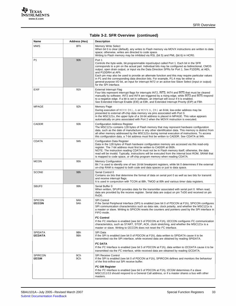
www.ti.com
SFR Overview
Table 3-2. SFR Overview (continued)Name Address (Hex) Description
MWS 8Fh Memory Write SelectWhen bit 0 is clear (default), any writes to Flash memory via MOVX instructions are written to dataspace; otherwise, writes are directed to code space.Writing to Flash memory may be inhibited via RSL (bit 5) and PML (bit 6) in HCR0.
P1 90h Port 1Controls the byte-wide, bit-programmable input/output called Port 1. Each bit in the SFRcorresponds to a pin on the actual part. Individual bits may be configured as bidirectional, CMOSoutput, open drain output, or input via the Data Direction SFRs for Port 1. See P1DDRL at AEh,and P1DDRH at AFh.Each pin may also be used to provide an alternate function and this may require particular valuesin P1 and the corresponding data direction bits. For example, P1.4 may be either ageneral-purpose I/O bit, an input for interrupt INT2 or an active-low Slave Select (input or output)for the SPI interface.
EXIF 91h External Interrupt FlagFour bits represent interrupt flags for interrupts INT2, INT3, INT4 and INT5 that must be clearedmanually by software. INT2 and INT4 are triggered by a rising edge, while INT3 and INT5 respondto a negative edge. If a bit is set in software, an interrupt will occur if it is enabled.See Extended Interrupt Enable (EIE) at E8h, and Extended Interrupt Priority (EIP) at FBh
MPAGE 92h Memory PageDuring execution of MOVX @Ri,A or MOVX A,@Ri an 8-bit, low-order address may bepresented to external off-chip data memory via pins associated with Port 0.In the MSC121x, the upper byte of a 16-bit address is placed in MPAGE. This value appearsautomatically on pins associated with Port 2 when the MOVX instruction is executed.
CADDR 93h Configuration Address RegisterThe MSC121x contains 128 bytes of Flash memory that may represent hardware configurationdata, such as the date of manufacture or any other identification data. This memory is distinct fromall other memory addressed by the MSC121x during normal execution of instructions. To accessthis configuration data, a 7-bit address must first be written to CADDR. See CDATA at 94h.
CDATA 94h Configuration Data RegisterData in the 128 bytes of Flash hardware configuration memory are accessed via this read-onlyregister. The 7-bit address must first be written to CADDR at 093h.NOTE: The instruction reading CDATA must not be in Flash memory itself; otherwise, the dataread will be invalid. Typically, instructions will be executed from the internal boot ROM, SRAM thatis mapped to code space, or off-chip program memory when reading CDATA.
MCON 95h Memory ConfigurationBit 7 is used to identify one of two 16-bit breakpoint registers, while bit 0 determines if the externalon-chip RAM is mapped to both code and data spaces or just to data space.
SCON0 98h Serial Control 0Contains six bits that determine the format of data on serial port 0 as well as two bits for transmitand receive interrupt flags.It is used in conjunction with TCON at 88h, TMOD at 89h and various timer data registers.
SBUF0 99h Serial Buffer 0When written, SFUF0 provides data for the transmitter associated with serial port 0. When read,data are provided by the receive register. Serial data are output on pin TxD0 and received on pinRxD0.
SPICON 9Ah SPI ControlI2CCON 9Ah If the Serial Peripheral Interface (SPI) is enabled (see bit 0 of PDCON at F1h), SPICON configures
SPI communication characteristics such as data rate, clock polarity, and whether the MSC121x isa master or slave. Writing to SPICON resets the counters and pointers used by the SPI interface inFIFO mode.
I2C ControlIf the I2C interface is enabled (see bit 5 of PDCON at F1h), I2CCON configures I2C communicationcharacteristics, such as START, STOP, ACK, clock stretching, and whether the MSC121x is amaster or slave. Writing to I2CCON does not reset the I2C interface.
SPIDATA 9Bh SPI DataI2CDATA 9Bh If the SPI is enabled (see bit 0 of PDCON at F1h), data written to SPIDATA cause it to be
transmitted via the SPI interface, while received data are obtained by reading SPIDATA.
I2C DATAIf the I2C Interface is enabled (see bit 5 of PDCON at F1h), data written to I2CDATA cause it to betransmitted via the I2C interface, while received data are obtained by reading I2CDATA.
SPIRCON 9Ch SPI Receive ControlI2CGM 9Ch If the SPI is enabled (see bit 0 of PDCON at F1h), SPIRCON defines and monitors the behaviour
of the first-in/first-out SPI receive buffer.
I2C GM RegisterIf the I2C interface is enabled (see bit 5 of PDCON at F1h), I2CGM determines if a slaveMSC1211/13 should respond to a General Call address, or if a master shares a bus with othermasters.
SBAU101A–July 2005–Revised March 2007 Special Function Registers 33Submit Documentation Feedback
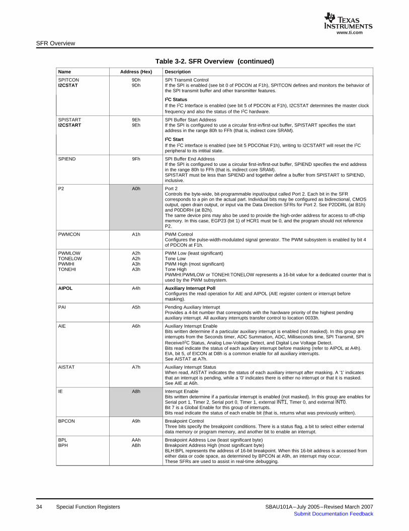
www.ti.com
SFR Overview
Table 3-2. SFR Overview (continued)Name Address (Hex) Description
SPITCON 9Dh SPI Transmit ControlI2CSTAT 9Dh If the SPI is enabled (see bit 0 of PDCON at F1h), SPITCON defines and monitors the behavior of
the SPI transmit buffer and other transmitter features.
I2C StatusIf the I2C Interface is enabled (see bit 5 of PDCON at F1h), I2CSTAT determines the master clockfrequency and also the status of the I2C hardware.
SPISTART 9Eh SPI Buffer Start AddressI2CSTART 9Eh If the SPI is configured to use a circular first-in/first-out buffer, SPISTART specifies the start
address in the range 80h to FFh (that is, indirect core SRAM).
I2C StartIf the I2C interface is enabled (see bit 5 PDCONat F1h), writing to I2CSTART will reset the I2Cperipheral to its intitial state.
SPIEND 9Fh SPI Buffer End AddressIf the SPI is configured to use a circular first-in/first-out buffer, SPIEND specifies the end addressin the range 80h to FFh (that is, indirect core SRAM).SPISTART must be less than SPIEND and together define a buffer from SPISTART to SPIEND,inclusive.
P2 A0h Port 2Controls the byte-wide, bit-programmable input/output called Port 2. Each bit in the SFRcorresponds to a pin on the actual part. Individual bits may be configured as bidirectional, CMOSoutput, open drain output, or input via the Data Direction SFRs for Port 2. See P2DDRL (at B1h)and P0DDRH (at B2h).The same device pins may also be used to provide the high-order address for access to off-chipmemory. In this case, EGP23 (bit 1) of HCR1 must be 0, and the program should not referenceP2.
PWMCON A1h PWM ControlConfigures the pulse-width-modulated signal generator. The PWM subsystem is enabled by bit 4of PDCON at F1h.
PWMLOW A2h PWM Low (least significant)TONELOW A2h Tone LowPWMHI A3h PWM High (most significant)TONEHI A3h Tone High
PWMHI:PWMLOW or TONEHI:TONELOW represents a 16-bit value for a dedicated counter that isused by the PWM subsystem.
AIPOL A4h Auxiliary Interrupt PollConfigures the read operation for AIE and AIPOL (AIE register content or interrupt beforemasking).
PAI A5h Pending Auxiliary InterruptProvides a 4-bit number that corresponds with the hardware priority of the highest pendingauxiliary interrupt. All auxiliary interrupts transfer control to location 0033h.
AIE A6h Auxiliary Interrupt EnableBits written determine if a particular auxiliary interrupt is enabled (not masked). In this group areinterrupts from the Seconds timer, ADC Summation, ADC, Milliseconds time, SPI Transmit, SPIReceive/I2C Status, Analog Low-Voltage Detect, and Digital Low Voltage Detect.Bits read indicate the status of each auxiliary interrupt before masking (refer to AIPOL at A4h).EIA, bit 5, of EICON at D8h is a common enable for all auxiliary interrupts.See AISTAT at A7h.
AISTAT A7h Auxiliary Interrupt StatusWhen read, AISTAT indicates the status of each auxiliary interrupt after masking. A '1' indicatesthat an interrupt is pending, while a '0' indicates there is either no interrupt or that it is masked.See AIE at A6h.
IE A8h Interrupt EnableBits written determine if a particular interrupt is enabled (not masked). In this group are enables forSerial port 1, Timer 2, Serial port 0, Timer 1, external INT1, Timer 0, and external INT0.Bit 7 is a Global Enable for this group of interrupts.Bits read indicate the status of each enable bit (that is, returns what was previously written).
BPCON A9h Breakpoint ControlThree bits specify the breakpoint conditions. There is a status flag, a bit to select either externaldata memory or program memory, and another bit to enable an interrupt.
BPL AAh Breakpoint Address Low (least significant byte)BPH ABh Breakpoint Address High (most significant byte)
BLH:BPL represents the address of 16-bit breakpoint. When this 16-bit address is accessed fromeither data or code space, as determined by BPCON at A9h, an interrupt may occur.These SFRs are used to assist in real-time debugging.
34 Special Function Registers SBAU101A–July 2005–Revised March 2007Submit Documentation Feedback
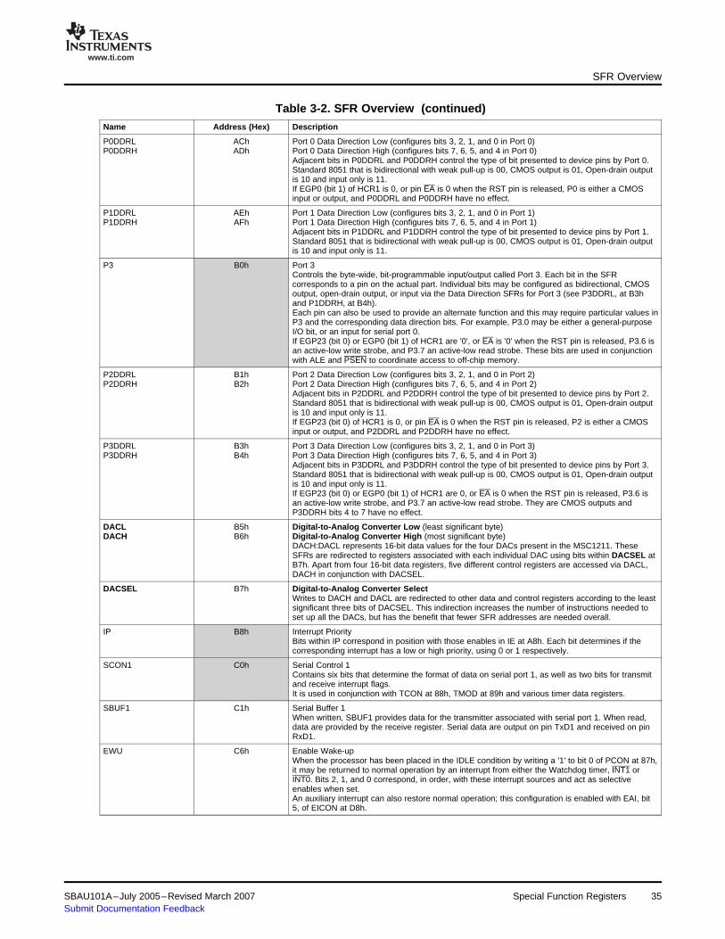
www.ti.com
SFR Overview
Table 3-2. SFR Overview (continued)Name Address (Hex) Description
P0DDRL ACh Port 0 Data Direction Low (configures bits 3, 2, 1, and 0 in Port 0)P0DDRH ADh Port 0 Data Direction High (configures bits 7, 6, 5, and 4 in Port 0)
Adjacent bits in P0DDRL and P0DDRH control the type of bit presented to device pins by Port 0.Standard 8051 that is bidirectional with weak pull-up is 00, CMOS output is 01, Open-drain outputis 10 and input only is 11.If EGP0 (bit 1) of HCR1 is 0, or pin EA is 0 when the RST pin is released, P0 is either a CMOSinput or output, and P0DDRL and P0DDRH have no effect.
P1DDRL AEh Port 1 Data Direction Low (configures bits 3, 2, 1, and 0 in Port 1)P1DDRH AFh Port 1 Data Direction High (configures bits 7, 6, 5, and 4 in Port 1)
Adjacent bits in P1DDRL and P1DDRH control the type of bit presented to device pins by Port 1.Standard 8051 that is bidirectional with weak pull-up is 00, CMOS output is 01, Open-drain outputis 10 and input only is 11.
P3 B0h Port 3Controls the byte-wide, bit-programmable input/output called Port 3. Each bit in the SFRcorresponds to a pin on the actual part. Individual bits may be configured as bidirectional, CMOSoutput, open-drain output, or input via the Data Direction SFRs for Port 3 (see P3DDRL, at B3hand P1DDRH, at B4h).Each pin can also be used to provide an alternate function and this may require particular values inP3 and the corresponding data direction bits. For example, P3.0 may be either a general-purposeI/O bit, or an input for serial port 0.If EGP23 (bit 0) or EGP0 (bit 1) of HCR1 are '0', or EA is '0' when the RST pin is released, P3.6 isan active-low write strobe, and P3.7 an active-low read strobe. These bits are used in conjunctionwith ALE and PSEN to coordinate access to off-chip memory.
P2DDRL B1h Port 2 Data Direction Low (configures bits 3, 2, 1, and 0 in Port 2)P2DDRH B2h Port 2 Data Direction High (configures bits 7, 6, 5, and 4 in Port 2)
Adjacent bits in P2DDRL and P2DDRH control the type of bit presented to device pins by Port 2.Standard 8051 that is bidirectional with weak pull-up is 00, CMOS output is 01, Open-drain outputis 10 and input only is 11.If EGP23 (bit 0) of HCR1 is 0, or pin EA is 0 when the RST pin is released, P2 is either a CMOSinput or output, and P2DDRL and P2DDRH have no effect.
P3DDRL B3h Port 3 Data Direction Low (configures bits 3, 2, 1, and 0 in Port 3)P3DDRH B4h Port 3 Data Direction High (configures bits 7, 6, 5, and 4 in Port 3)
Adjacent bits in P3DDRL and P3DDRH control the type of bit presented to device pins by Port 3.Standard 8051 that is bidirectional with weak pull-up is 00, CMOS output is 01, Open-drain outputis 10 and input only is 11.If EGP23 (bit 0) or EGP0 (bit 1) of HCR1 are 0, or EA is 0 when the RST pin is released, P3.6 isan active-low write strobe, and P3.7 an active-low read strobe. They are CMOS outputs andP3DDRH bits 4 to 7 have no effect.
DACL B5h Digital-to-Analog Converter Low (least significant byte)DACH B6h Digital-to-Analog Converter High (most significant byte)
DACH:DACL represents 16-bit data values for the four DACs present in the MSC1211. TheseSFRs are redirected to registers associated with each individual DAC using bits within DACSEL atB7h. Apart from four 16-bit data registers, five different control registers are accessed via DACL,DACH in conjunction with DACSEL.
DACSEL B7h Digital-to-Analog Converter SelectWrites to DACH and DACL are redirected to other data and control registers according to the leastsignificant three bits of DACSEL. This indirection increases the number of instructions needed toset up all the DACs, but has the benefit that fewer SFR addresses are needed overall.
IP B8h Interrupt PriorityBits within IP correspond in position with those enables in IE at A8h. Each bit determines if thecorresponding interrupt has a low or high priority, using 0 or 1 respectively.
SCON1 C0h Serial Control 1Contains six bits that determine the format of data on serial port 1, as well as two bits for transmitand receive interrupt flags.It is used in conjunction with TCON at 88h, TMOD at 89h and various timer data registers.
SBUF1 C1h Serial Buffer 1When written, SBUF1 provides data for the transmitter associated with serial port 1. When read,data are provided by the receive register. Serial data are output on pin TxD1 and received on pinRxD1.
EWU C6h Enable Wake-upWhen the processor has been placed in the IDLE condition by writing a '1' to bit 0 of PCON at 87h,it may be returned to normal operation by an interrupt from either the Watchdog timer, INT1 orINT0. Bits 2, 1, and 0 correspond, in order, with these interrupt sources and act as selectiveenables when set.An auxiliary interrupt can also restore normal operation; this configuration is enabled with EAI, bit5, of EICON at D8h.
SBAU101A–July 2005–Revised March 2007 Special Function Registers 35Submit Documentation Feedback
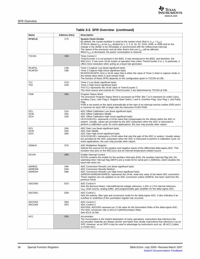
www.ti.com
SFR Overview
Table 3-2. SFR Overview (continued)Name Address (Hex) Description
SYSCLK C7h System Clock DividerBy default, the crystal oscillator is used as the system clock (that is, fCLK = fOSC).SYSCLK allows fCLK to be fOSC divided by 1, 2, 4, 8, 16, 32, 1024, 2048, or 4096 and for thechange in the divider to be immediate or synchronized with the milliseconds interrupt.The speed of the processor and all other timers that use fCLK will be affected.When fCLK is decreased, the power consumption is reduced.
T2CON C8h Timer Control 2Timer/Counter 2 is not present in the 8051. It was introduced in the 8052, and therefore, theMSC121x. It has more 16-bit modes of operation than either Timer/Counter 0 or 1. In particular, itoffers more resolution when acting as a baud rate generator.
RCAP2L CAh Timer 2 Capture Low (least significant byte)RCAP2H CBh Timer 2 Capture High (most significant byte)
RCAP2H:RCAP2L form a 16-bit value that is either the value of Timer 2 when in capture mode orthe reload value when in auto-reload mode.The function of these SFRs depends on the configuration given in T2CON at C8h.
TL2 CCh Timer 2 Low (least significant byte)TH2 CDh Timer 2 High (most significant byte)
TH2:TL2 represents the 16-bit value of Timer/Counter 2.The clock source and controls for Timer/Counter 2 are determined by T2CON at C8h.
PSW D0h Program Status WordThe processor Program Status Word is accessed via PSW. Bits 7 to 0 represent (in order) Carry,Auxiliary Carry, User Flag 0, Register Bank Select 1 and 0, Overflow Flag, User Flag 1, and ParityFlag.PSW is not saved on the stack automatically at the start of an interrupt service routine (ISR) and itis common for each ISR to begin with the instruction PUSH PSW.
OCL D1h ADC Offset Calibration Low (least significant byte)OCM D2h ADC Offset Calibration MiddleOCH D3h ADC Offset Calibration High (most significant byte)
OCH:OCM:OCL represents a 24-bit value that compensates for the offsets within the ADC orsystem. Usually, values are provided by the ADC subsystem when the ADC is instructed toperform a calibration cycle; for some applications, the user may provide other values.
GCL D4h ADC Gain Low (least significant byte)GCM D5h ADC Gain MiddleGCH D6h ADC Gain High (most significant byte)
GCH:GCM:GCL represents a 24-bit value that sets the gain of the ADC or system. Usually valuesare provided by the ADC subsystem when the ADC is instructed to perform a calibration cycle; forsome applications, the user may provide other values.
ADMUX D7h ADC Multiplexer RegisterSelects the sources for the positive and negative inputs of the differential delta-sigma ADC. Thisincludes nine pins on the MSC121x and an internal temperature-related source.
EICON D8h Enable Interrupt ControlEICON contains the enable for the auxiliary interrupts (EAI), the auxiliary interrupt flag (AI), thewatchdog timer interrupt flag (WDTI) and a mode bit for serial port 1 (SMOD1), which doubles thebaud rate when set.
ADRESL D9h ADC Conversion Results Low (least significant byte)ADRESM DAh ADC Conversion Results MediumADRESH DBh ADC Conversion Results Low High (most significant byte)
ADRESH:ADRESM:ADRESL represents the 24-bit, read-only value of the latest ADC conversion.These registers are not updated on an ADC conversion unless ADRESL has been read from theprevious result.
ADCON0 DCh ADC Control 0Sets the Burnout Detect, Internal/External voltage reference, 1.25V or 2.5V internal reference,VREF clock source, analog buffer, and programmable gain amplifier for the delta-sigma ADC.
ADCON1 DDh ADC Control 1Sets the polarity, filter type and conversion mode for the delta-sigma ADC. It also indicates if anoverflow or underflow of the summation register has occurred.
ADCON2 DEh ADC Control 2ADCON3 DFh ADC Control 3
ADCON3: ADCON2 represent an 11-bit value for the Decimation Ratio of the delta-sigma ADC.The ADC conversion rate is (ACLK+1)/64/Decimation Ratio.See ACLK at F6h.
ACC E0h AccumulatorThe Accumulator is the implicit destination of many operations. Instructions that reference theAccumulator implicitly are always shorter and faster than similar instructions that reference it as anSFR. However, as an SFR it may be used to advantage by instructions such as: JB ACC.2,label,or PUSH ACC.
36 Special Function Registers SBAU101A–July 2005–Revised March 2007Submit Documentation Feedback

www.ti.com
SFR Overview
Table 3-2. SFR Overview (continued)Name Address (Hex) Description
SSCON E1h Summation and Shift ControlThe result of an ADC conversion is placed in ADRES (D9h to DBh), but may be automaticallyadded to a 32-bit sum represented by SUMR (E2h to E5h). The operation of the summationregister is controlled by SSCON, which includes the number of times ADC conversions are addedto the sum, and the number of bits that the sum is shifted to the right.There is also a mode where 32-bit values provided by the CPU may be added to, or subtractedfrom (MSC1211/12/13/14 only), the summation register when SUMR0 is written.If 00h is written to SSCON, the 32-bit summation register is cleared.
SUMR0 E2h Summation Register 0 (least significant byte)SUMR1 E3h Summation Register 1SUMR2 E4h Summation Register 2SUMR3 E5h Summation Register 3 (most significant byte)
SUMR3:SUMR2:SUMR1:SUMR0 represent the 32-bit sum (and optional shift) of a number of ADCconversions.See SSCON at E1h.
ODAC E6h (ADC) Offset DAC RegisterAn analog voltage of up to ± half the range of the ADC is set with an 8-bit DAC and used to offsetthe input voltage to the ADC.The ODAC register cannot be used to to extend the analog inputs beyond their specified inputrange.
LVDCON E7h Low-Voltage Detection ControlThe voltages present on the analog and digital supply pins may be enabled to generate interruptsif they fall below preset limits. For either analog or digital, the limits are 2.7V, 3.0V, 3.3V, 4.0V,4.2V, 4.5V, and 4.7V.The analog low-voltage interrupt may be generated if AIN7 falls below 1.2V, while the digitallow-voltage interrupt may be generated if AIN6 falls below 1.2V. This function provides a means ofdetecting an impending power-fail condition while the supply pins themselves are still valid. It canalso be used to measure other voltages.
EIE E8h Extended Interrupt EnableProvides selective enables for the watchdog timer, INT5, INT4, INT3, and INT2.See WDTI, bit 3, in EICON at D8h.See External Interrupt Flags, EXIF at 91h.
HWPC0 E9h Hardware Product Code 0Refer to the respective data sheet for the code that indicates the type of device.
HWPC1 EAh Hardware Product Code 1Refer to the respective data sheet for the code that indicates the type of device.
HDWVER EBh Hardware Version NumberRefer to the respective data sheet for the code that indicates the type of device.
FMCON EEh Flash Memory ControlThree bits to provide control of the Flash memory; specifically, page mode erase, frequency controlmode, and busy.
FTCON EFh Flash Memory Timing ControlThe upper four bits (FER) determine the Flash erase time while the lower four bits (FWR)determine the Flash write time, according to the following equations:Erase time = (1 + FER) × (MSECH:MSECL + 1) × tCLK5 ms (11ms) for commercial (industrial) temperaturesWrite time = 5 × (1 + FWR) × (USEC + 1) × tCLKThe write time should be between 30µs and 40µs.See MSECH and MSECL at FDh and FCh, respectively, and USEC at FBh.
B F0h B RegisterThe B register is used only by the instructions MUL AB and DIV AB.If these instructions are not used, B is available to store a byte-wide variable or eight single-bitvariables.Caution is needed when programming in C because run-time libraries may use these instructions,and thus corrupt the value in B.
PDCON F1h Power-Down ControlActive high bits within PDCON provide selective power-down of subsystems DAC, I2C, PWM,ADC, Watchdog, System Timer, and SPI.
PASEL F2h PSEN/ALE SelectWhen off-chip memory is not used, control signals PSEN and ALE are not needed.Three bits in PASEL allow the pin associated with PSEN to be either the usual PSEN signal,system clock, ADC modulator clock, low or high.Two other bits allow the pin associated with ALE to be either the usual ALE signal, low or high.NOTE: When these two lines are used as output lines, they should be lightly loaded to avoidentering serial or parallel flash programming modes on reset.
ACLK F6h Analog ClockThe frequency of the delta-sigma ADC modulator is given by:fCLK/(ACLK + 1) × 64where fCLK is the frequency of the system clock.
SBAU101A–July 2005–Revised March 2007 Special Function Registers 37Submit Documentation Feedback

www.ti.com
SFR Overview
Table 3-2. SFR Overview (continued)Name Address (Hex) Description
SRST F7h System Reset RegisterIf bit 0 is set high then low, the MSC121x will be reset. This sequence causes exactly the samebehavior as if a system reset had been initiated by the RST pin. ALE, PSEN, and EA will besampled after the power-up delay.
EIP F8h Extended Interrupt PriorityFive bits determine the priority for interrupts: Watchdog, INT5, INT4, INT3, and INT2.See Extended Interrupt Flags, EXIF, at 91h and Extended Interrupt Enable, EIE, at E8h.
SECINT F9h Seconds Timer InterruptThe seconds interrupt, if enabled, occurs at an interval given by:(SECINT + 1) × (HMSEC + 1) × (MSEC + 1) × tCLKIf bit 7 is set when SECINT is written, the SECINT value will be loaded into the counterimmediately; otherwise, it will be delayed until the current count expires.When the associated down-counter reaches zero, it is reloaded with the value in SECINT.See Bit 7, ESEC, of AIE at A6h.
MSINT FAh Milliseconds InterruptThe milliseconds interrupt, if enabled, occurs with an interval given by:(MSINT + 1) × (MSEC + 1) × tCLKIf bit 7 is set when MSINT is written, the MSINT value will be loaded into the counter immediately;otherwise, it will be delayed until the current count expires.When the associated down-counter reaches zero, it is reloaded with the value in MSINT.See Bit 4, EMSEC, of AIE at A6h.
USEC FBh Microsecond RegisterThe internal microseconds clock has a period given by:(USEC + 1) × tCLK = (USEC + 1)/fCLKWhen the associated down-counter reaches zero, it is reloaded with the value in USEC.See FTCON at EFh.
MSECL FCh Millisecond LowMSECH FDh Millisecond High
MSECH:MSECL together represent MSEC, which determines the time between millisecondinterrupts given by:(MSECH × 256 + MSECL + 1) × tCLKWhen the associated down-counter reaches zero, it is reloaded with the value in MSECH:MSECL.
HMSEC FEh Hundred Millisecond ClockThe hundred milliseconds counter has a period given by:(HMSEC + 1) × (MSECH × 256 + MSECL + 1) × tCLKWhen the associated down-counter reaches zero, it is reloaded with the value in HMSEC.
WDTCON FFh Watchdog ControlOnce enabled, the watchdog timer expires after a delay of:(WDCNT + 1) y HMSEC to (WDCNT + 2) y HMSECWriting a '1', then '0' sequence to bit 7, bit 6, or bit 5 enables, disables, or restarts the watchdogtimer, respectively.If the associated down-counter reaches zero, a watchdog timeout occurs. By default, this timeoutcauses a reset, but EWDR (bit 3) in HCR0 may disable the reset and trigger an interrupt instead.During normal operation, the counter must be repeatedly restarted before it reaches zero.
38 Special Function Registers SBAU101A–July 2005–Revised March 2007Submit Documentation Feedback
Chapter 4SBAU101A–July 2005–Revised March 2007
Programmer's Model and Instruction Set
This chapter describes the programmer’s model and instruction set for the MSC121x.
Topic ........................................................................................................... Page
4.1 Introduction....................................................................................... 404.2 Registers .......................................................................................... 414.3 Instruction Types and Addressing Modes ............................................. 424.4 MSC121x Op-Code Table .................................................................... 464.5 Example of MSC121x Instructions........................................................ 48
SBAU101A–July 2005–Revised March 2007 Programmer's Model and Instruction Set 39Submit Documentation Feedback

www.ti.com
4.1 Introduction
Introduction
The MSC121x incorporates a microcontroller with the same instruction set as the industry-standard 8051;however, for a given external clock, it executes up to three times more quickly. This increased rate isbecause the MSC121x is based on a machine cycle of four clocks rather than the original 12.
Although the most frequently-used instructions are three times faster, the aggregate speed improvementfor programs written in C language is about 2.3 times faster.
If application programs are written in C, the programmer has little control over the compiler's choice ofinstructions; however, for efficient, hard real-time operations, assembly-level routines can be achieved thatapproach a 3x rate increase over the 8051.
40 Programmer's Model and Instruction Set SBAU101A–July 2005–Revised March 2007Submit Documentation Feedback

www.ti.com
4.2 Registers
Registers
The MSC121x manipulates data via a single 8-bit accumulator (A), together with eight 8-bit registers (R0to R7). The result of all arithmetic and logical operations is placed in the accumulator, which can then becopied to Rn, on-chip memory, or off-chip memory, by various MOV instructions.
To the programmer, the MSC121x may be modelled as shown in Table 4-1.
Table 4-1. 8051 Working RegistersBit
Name15 14 13 12 11 10 9 8 7 6 5 4 3 2 1 0
PSW CY AC F0 RS1 RS0 OV F1 P
B Register B
Rn Register n (where n = 0 to 7)
A Accumulator
DPL Data Pointer Low
DPH Data Pointer High
SP Stack Pointer
DPTR Data Pointer High Data Pointer Low
PC Program Counter
The Data Pointer (DPTR) is composed of two 8-bit SFRs accessed as separate bytes. However, it is usedimplicitly by some instructions as a 16-bit pointer to either program or data memory.
The Stack Pointer (SP) is used to support a first-in/first-out data structure within core data memory. Whenreferenced implicitly as an 8-bit pointer, it is pre-incremented and post-decremented, which means that thestack grows upwards and SP always points to the most recent entry. The stack can store either datavalues or addresses.
The default value for SP is 7, so it starts to grow just above memory associated with address bank 0 atcore data memory locations 00h to 07h. Since address bank 1 occupies locations 08h to 0Fh, care mustbe taken to redefine the initial value of SP whenever register bank 1 (or 2 or 3) is to be used. Theselection of the active register bank is determined by bits 4 and 3 of the Program Status Word (PSW). Forexample, when RS1 = 1 and RS0 = 1, bank 3 is active and R2 corresponds with core data memorylocation 1Ah.
PSW also contains the Carry flag (CY), Auxiliary Carry (AC), and General-purpose flags F1 and F0, aswell as the Overflow flag (OV) and the Parity flag (P). Some instructions change the flags, but the majoritydo not.
Register B is sometimes useful to store a byte-wide variable or 8 bit-wide variables, especially forapplications written entirely in assembly language. Care is needed because this register is used by MULand DIV instructions that may be called by C run-time libraries.
The 16-bit program counter (PC) is incremented as sequential instructions are executed. For jumps, it isloaded with a new value; for CALLs and interrupts, it is stored to the stack for recovery during RETurnsand RETI. It always points to a byte in program memory and has a reset value of 0000h.
SBAU101A–July 2005–Revised March 2007 Programmer's Model and Instruction Set 41Submit Documentation Feedback
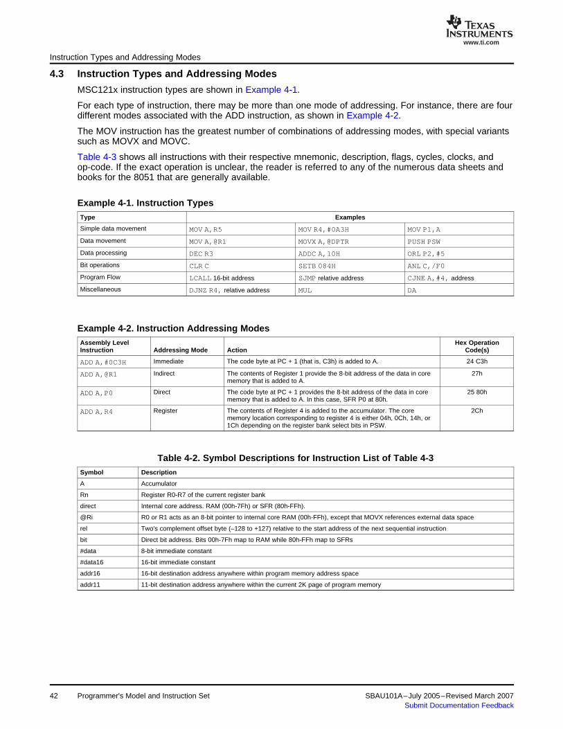
www.ti.com
4.3 Instruction Types and Addressing Modes
Instruction Types and Addressing Modes
MSC121x instruction types are shown in Example 4-1.
For each type of instruction, there may be more than one mode of addressing. For instance, there are fourdifferent modes associated with the ADD instruction, as shown in Example 4-2.
The MOV instruction has the greatest number of combinations of addressing modes, with special variantssuch as MOVX and MOVC.
Table 4-3 shows all instructions with their respective mnemonic, description, flags, cycles, clocks, andop-code. If the exact operation is unclear, the reader is referred to any of the numerous data sheets andbooks for the 8051 that are generally available.
Example 4-1. Instruction TypesType Examples
Simple data movement MOV A,R5 MOV R4,#0A3H MOV P1,A
Data movement MOV A,@R1 MOVX A,@DPTR PUSH PSW
Data processing DEC R3 ADDC A,10H ORL P2,#5
Bit operations CLR C SETB 084H ANL C,/F0
Program Flow LCALL 16-bit address SJMP relative address CJNE A,#4, address
Miscellaneous DJNZ R4, relative address MUL DA
Example 4-2. Instruction Addressing ModesAssembly Level Hex OperationInstruction Addressing Mode Action Code(s)
Immediate The code byte at PC + 1 (that is, C3h) is added to A. 24 C3hADD A,#0C3H
Indirect The contents of Register 1 provide the 8-bit address of the data in core 27hADD A,@R1memory that is added to A.
Direct The code byte at PC + 1 provides the 8-bit address of the data in core 25 80hADD A,P0memory that is added to A. In this case, SFR P0 at 80h.
Register The contents of Register 4 is added to the accumulator. The core 2ChADD A,R4memory location corresponding to register 4 is either 04h, 0Ch, 14h, or1Ch depending on the register bank select bits in PSW.
Table 4-2. Symbol Descriptions for Instruction List of Table 4-3Symbol Description
A Accumulator
Rn Register R0-R7 of the current register bank
direct Internal core address. RAM (00h-7Fh) or SFR (80h-FFh).
@Ri R0 or R1 acts as an 8-bit pointer to internal core RAM (00h-FFh), except that MOVX references external data space
rel Two's complement offset byte (–128 to +127) relative to the start address of the next sequential instruction
bit Direct bit address. Bits 00h-7Fh map to RAM while 80h-FFh map to SFRs
#data 8-bit immediate constant
#data16 16-bit immediate constant
addr16 16-bit destination address anywhere within program memory address space
addr11 11-bit destination address anywhere within the current 2K page of program memory
42 Programmer's Model and Instruction Set SBAU101A–July 2005–Revised March 2007Submit Documentation Feedback

www.ti.com
Instruction Types and Addressing Modes
Table 4-3. Instruction ListFlags (1)
MSC121x MSC121x 8051 CodeMnemonic Description CY AC OV Bytes Cycles Clocks Clocks (Hex)
Arithmetic
ADD A,Rn Add register to A X X X 1 1 4 12 28-2F
ADD A,direct Add direct byte to A X X X 2 2 8 12 25
ADD A,@Ri Add indirect data memory to A X X X 1 1 4 12 26-27
ADD A,#data Add immediate data to A X X X 2 2 8 12 24
ADDC A,Rn Add register to A with carry X X X 1 1 4 12 38-3F
ADDC A,direct Add direct byte to A with carry X X X 2 2 8 12 35
ADDC A,@Ri Add indirect data memory to A with carry X X X 1 1 4 12 36-37
ADDC A,#data Add immediate data to A with carry X X X 2 2 8 12 34
SUBB A,Rn Subtract register from A with borrow X X X 1 1 4 12 98-9F
SUBB A,direct Subtract direct byte from A with borrow X X X 2 2 8 12 95
SUBB A,@Ri Subtract indirect data memory from A X X X 1 1 4 12 96-97with borrow
SUBB A,#data Subtract immediate data from A with X X X 2 2 8 12 94borrow
INC A Increment A - - - 1 1 4 12 04
INC Rn Increment register - - - 1 1 4 12 08-0F
INC direct Increment direct byte - - - 2 2 8 12 05
INC @Ri Increment indirect data memory - - - 1 1 4 12 06-07
DEC A Decrement A - - - 1 1 4 12 14
DEC Rn Decrement register - - - 1 1 4 12 18-1F
DEC direct Decrement direct byte - - - 2 2 8 12 15
DEC @Ri Decrement indirect data memory - - - 1 1 4 12 16-17
INC DPTR Increment 16-bit data pointer - - - 1 3 12 24 A3
MUL AB Multiply A by B 0 - X 1 5 20 48 A4
DIV AB Divide A by B 0 - X 1 5 20 48 84
DA A Decimal adjust A to give 2 BCD nibbles. X - - 1 1 4 12 D4Used after ADD or ADDC.
Logical
ANL A,Rn AND register to A - - - 1 1 4 12 58-5F
ANL A,direct AND direct byte to A - - - 2 2 8 12 55
ANL A,@Ri AND indirect data memory to A - - - 1 1 4 12 56-57
ANL A,#data AND immediate data to A - - - 2 2 8 12 54
ANL direct,A AND A to direct byte - - - 2 2 8 12 52
ANL direct,#data AND immediate data to direct byte - - - 3 3 12 24 53
ORL A,Rn OR register to A - - - 1 1 4 12 48-4F
ORL A,direct OR direct byte to A - - - 2 2 8 12 45
ORL A,@Ri OR indirect data memory to A - - - 1 1 4 12 46-47
ORL A,#data OR immediate data to A - - - 2 2 8 12 44
ORL direct,A OR A to direct byte - - - 2 2 8 12 42
ORL direct,#data OR immediate data to direct byte - - - 3 3 12 24 43
XRL A,Rn Exclusive OR register to A - - - 1 1 4 12 68-6F
XRL A,direct Exclusive OR direct byte to A - - - 2 2 8 12 65
XRL A,@Ri Exclusive OR indirect data memory to A - - - 1 1 4 12 66-67
XRL A,#data Exclusive OR immediate data to A - - - 2 2 8 12 64
XRL direct,A Exclusive OR A to direct byte - - - 2 2 8 12 62
XRL direct,#data Exclusive OR immediate data to direct - - - 3 3 12 24 63byte
CLR A Clear A - - - 1 1 4 12 E4
CPL A Complement A - - - 1 1 4 12 F4
(1) Flags CY, AC, and OV may also be changed by explicit writes to corresponding bits in the PSW.
SBAU101A–July 2005–Revised March 2007 Programmer's Model and Instruction Set 43Submit Documentation Feedback

www.ti.com
Instruction Types and Addressing Modes
Table 4-3. Instruction List (continued)Flags (1)
MSC121x MSC121x 8051 CodeMnemonic Description CY AC OV Bytes Cycles Clocks Clocks (Hex)
RL A Rotate A left - - - 1 1 4 12 23
RLC A Rotate A left through carry X - - 1 1 4 12 33
RR A Rotate A right - - - 1 1 4 12 03
RRC A Rotate A right through carry X - - 1 1 4 12 13
SWAP A Swap nibbles of A - - - 1 1 4 12 C4
Data Movement
MOV A,Rn Move register to A - - - 1 1 4 12 E8-EF
MOV A,direct Move direct byte to A - - - 2 2 8 12 E5
MOV A,@Ri Move indirect data memory to A - - - 1 1 4 12 E6-E7
MOV A,#data Move immediate data to A - - - 2 2 8 12 74
MOV Rn,A Move A to register - - - 1 1 4 12 F8-FF
MOV Rn,direct Move direct byte to register - - - 2 2 8 24 A8-AF
MOV Rn,#data Move immediate data to register - - - 2 2 8 12 78-7F
MOV direct,A Move A to direct byte - - - 2 2 8 12 F5
MOV direct,Rn Move register to direct byte - - - 2 2 8 24 88-8F
MOV direct,direct Move direct byte to direct byte - - - 3 3 12 24 85
MOV direct,@Ri Move indirect data memory to direct byte - - - 2 2 12 24 86-87
MOV direct,#data Move immediate data to direct byte - - - 3 3 12 24 75
MOV @Ri,A MOV A to indirect data memory - - - 1 1 4 12 F6-F7
MOV @Ri,direct Move direct byte to indirect data memory - - - 2 2 8 24 A6-A7
MOV @Ri,#data Move immediate data to indirect data - - - 2 2 8 12 76-77memory
MOV DPTR,#data Move 2 bytes of immediate data to data - - - 3 3 12 24 90pointer
MOVC A,@A+DPTR Move a byte in code space A (unsigned) - - - 1 3 12 24 93after DPTR to A
MOVC A,@A+PC Move a byte in code space A (unsigned) - - - 1 3 12 24 83after from the address of the nextinstruction to A
MOVX A,@Ri Move external data (A8) to A - - - 1 2-9 (2) 8 12 E2-E3
MOVX A,@DPTR Move external data (A16) to A - - - 1 2-9 (2) 8 24 E0
MOVX @Ri,A Move A to external data. Upper 8-bit - - - 1 2-9 (2) 8 24 F2-F3address comes from MPAGE SFR.
MOVX @DPTR,A Move A to external data memory - - - 1 2-9 (2) 8 24 F0
PUSH direct Push direct byte onto stack - - - 2 2 8 24 C0
POP direct Pop direct byte from stack - - - 2 2 8 24 D0
XCH A,Rn Exchange A and register - - - 1 1 4 12 C8-CF
XCH A,direct Exchange A and direct byte - - - 2 2 8 12 C5
XCH A,@Ri Exchange A and indirect data memory - - - 1 1 4 12 C6-C7
XCHD A,@Ri Exchange A and indirect data memory - - - 1 1 4 12 D6-D7nibble in bits 3-0
Boolean
CLR C Clear carry 0 - - 1 1 4 12 C3
CLR bit Clear direct bit - - - 2 2 8 12 C2
SETB C Set carry 1 - - 1 1 4 12 D3
SETB bit Set direct bit - - - 2 2 8 12 D2
CPL C Complement carry X - - 1 1 4 12 B3
CPL bit Complement direct bit - - - 2 2 8 12 B2
ANL C,bit AND direct bit to carry X - - 2 2 8 24 82
ANL C,/bit AND inverse of direct bit to carry X - - 2 2 8 24 B0
ORL C,bit OR direct bit to carry X - - 2 2 8 24 72
(2) Number of cycles is user-selectable; see SFR CKCON at 8Eh.
44 Programmer's Model and Instruction Set SBAU101A–July 2005–Revised March 2007Submit Documentation Feedback

www.ti.com
Instruction Types and Addressing Modes
Table 4-3. Instruction List (continued)Flags (1)
MSC121x MSC121x 8051 CodeMnemonic Description CY AC OV Bytes Cycles Clocks Clocks (Hex)
ORL C,/bit OR inverse of direct bit to carry X - - 2 2 8 24 A0
MOV C,bit Move direct bit to carry X - - 2 2 8 12 A2
MOV bit,C Move carry to direct bit - - - 2 2 8 24 92
Branching
ACALL addr11 Absolute call to subroutine within current - - - 2 3 12 24 11-F1page
LCALL addr16 Long call to subroutine; PC becomes - - - 3 4 16 24 12addr16.
RET Return from subroutine - - - 1 4 16 24 22
RETI Return from interrupt - - - 1 4 16 24 32
AJMP addr11 Absolute unconditional jump within - - - 2 3 12 24 01-E1current page
LJMP addr16 Long jump; PC becomes addr16. - - - 3 4 16 24 02
SJMP rel Unconditional relative jump - - - 2 3 12 24 80
JC rel Jump relative if carry is 1 - - - 2 3 12 24 40
JNC rel Jump relative if carry is 0 - - - 2 3 12 24 50
JB bit,rel Jump relative if direct bit is 1 - - - 3 4 16 24 20
JNB bit,rel Jump relative if direct bit is 0 - - - 3 4 16 24 30
JBC bit,rel Jump relative if direct bit is 1 and clear - - - 3 4 16 24 10the bit
JMP @A+DPTR Jump indirect. PC becomes DPTR plus A - - - 1 3 12 24 73
JZ rel Jump relative if accumulator is 00h - - - 2 3 12 24 60
JNZ rel Jump relative if accumulator is not 00h - - - 2 3 12 24 70
CJNE A,direct,rel Compare A with direct data and jump X - - 3 4 16 24 B5relative if not equal
CJNE A,#data,rel Compare A with immediate data and X - - 3 4 16 24 B4jump relative if not equal
CJNE Rn,#data,rel Compare register with immediate data x - - 3 4 16 24 B8-BFand jump relative if not equal
CJNE @Ri,#data,rel Compare indirect with immediate data x - - 3 4 16 24 B6-B7and jump relative if not equal
DJNZ Rn,rel Decrement register and jump relative if - - - 2 3 12 24 D8-DFnot 0
DJNZ direct,rel Decrement direct byte and jump relative if - - - 3 4 16 24 D5not 0
Miscellaneous
NOP No operation - - - 1 1 4 12 00
Reserved No operation - - - 1 1 4 12 A5
SBAU101A–July 2005–Revised March 2007 Programmer's Model and Instruction Set 45Submit Documentation Feedback
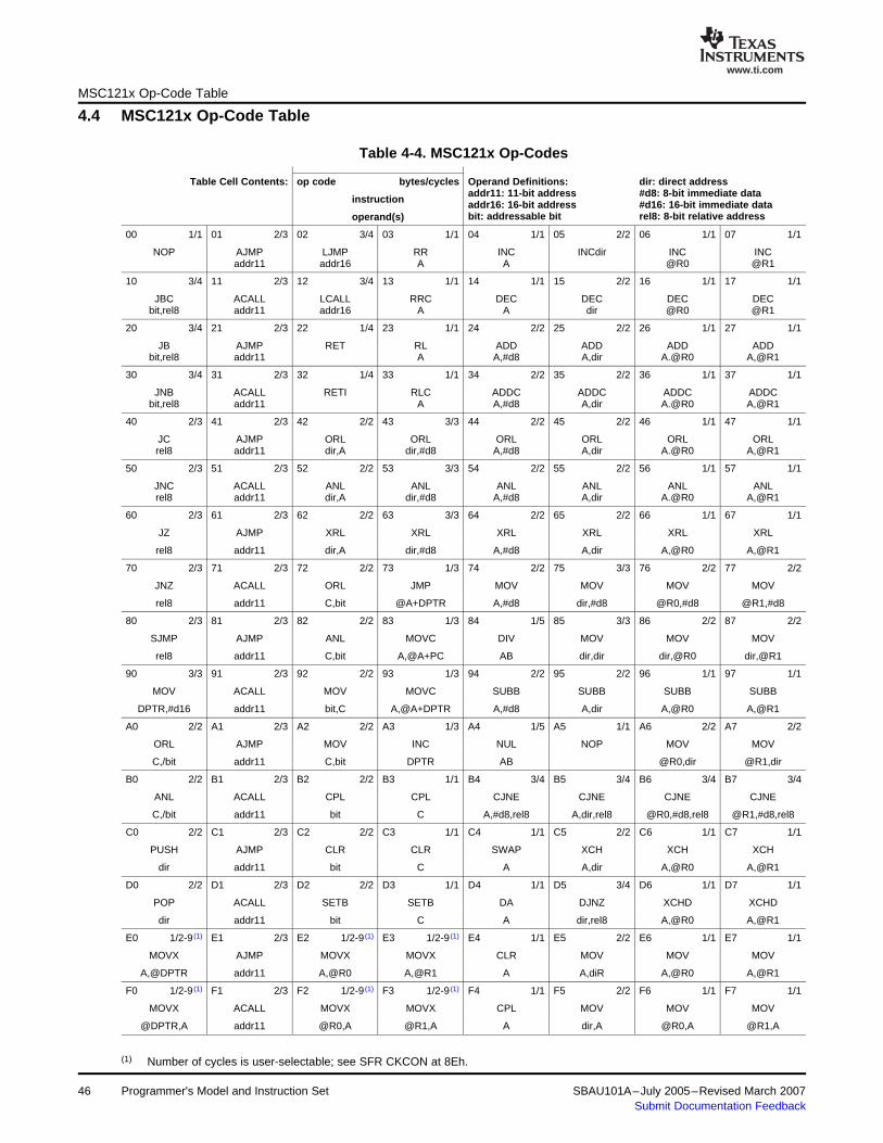
www.ti.com
4.4 MSC121x Op-Code TableMSC121x Op-Code Table
Table 4-4. MSC121x Op-Codes
Table Cell Contents: op code bytes/cycles Operand Definitions: dir: direct addressaddr11: 11-bit address #d8: 8-bit immediate data
instruction addr16: 16-bit address #d16: 16-bit immediate databit: addressable bit rel8: 8-bit relative addressoperand(s)
00 1/1 01 2/3 02 3/4 03 1/1 04 1/1 05 2/2 06 1/1 07 1/1
NOP AJMP LJMP RR INC INCdir INC INCaddr11 addr16 A A @R0 @R1
10 3/4 11 2/3 12 3/4 13 1/1 14 1/1 15 2/2 16 1/1 17 1/1
JBC ACALL LCALL RRC DEC DEC DEC DECbit,rel8 addr11 addr16 A A dir @R0 @R1
20 3/4 21 2/3 22 1/4 23 1/1 24 2/2 25 2/2 26 1/1 27 1/1
JB AJMP RET RL ADD ADD ADD ADDbit,rel8 addr11 A A,#d8 A,dir A.@R0 A,@R1
30 3/4 31 2/3 32 1/4 33 1/1 34 2/2 35 2/2 36 1/1 37 1/1
JNB ACALL RETI RLC ADDC ADDC ADDC ADDCbit,rel8 addr11 A A,#d8 A,dir A.@R0 A,@R1
40 2/3 41 2/3 42 2/2 43 3/3 44 2/2 45 2/2 46 1/1 47 1/1
JC AJMP ORL ORL ORL ORL ORL ORLrel8 addr11 dir,A dir,#d8 A,#d8 A,dir A.@R0 A,@R1
50 2/3 51 2/3 52 2/2 53 3/3 54 2/2 55 2/2 56 1/1 57 1/1
JNC ACALL ANL ANL ANL ANL ANL ANLrel8 addr11 dir,A dir,#d8 A,#d8 A,dir A.@R0 A,@R1
60 2/3 61 2/3 62 2/2 63 3/3 64 2/2 65 2/2 66 1/1 67 1/1
JZ AJMP XRL XRL XRL XRL XRL XRL
rel8 addr11 dir,A dir,#d8 A,#d8 A,dir A,@R0 A,@R1
70 2/3 71 2/3 72 2/2 73 1/3 74 2/2 75 3/3 76 2/2 77 2/2
JNZ ACALL ORL JMP MOV MOV MOV MOV
rel8 addr11 C,bit @A+DPTR A,#d8 dir,#d8 @R0,#d8 @R1,#d8
80 2/3 81 2/3 82 2/2 83 1/3 84 1/5 85 3/3 86 2/2 87 2/2
SJMP AJMP ANL MOVC DIV MOV MOV MOV
rel8 addr11 C,bit A,@A+PC AB dir,dir dir,@R0 dir,@R1
90 3/3 91 2/3 92 2/2 93 1/3 94 2/2 95 2/2 96 1/1 97 1/1
MOV ACALL MOV MOVC SUBB SUBB SUBB SUBB
DPTR,#d16 addr11 bit,C A,@A+DPTR A,#d8 A,dir A,@R0 A,@R1
A0 2/2 A1 2/3 A2 2/2 A3 1/3 A4 1/5 A5 1/1 A6 2/2 A7 2/2
ORL AJMP MOV INC NUL NOP MOV MOV
C,/bit addr11 C,bit DPTR AB @R0,dir @R1,dir
B0 2/2 B1 2/3 B2 2/2 B3 1/1 B4 3/4 B5 3/4 B6 3/4 B7 3/4
ANL ACALL CPL CPL CJNE CJNE CJNE CJNE
C,/bit addr11 bit C A,#d8,rel8 A,dir,rel8 @R0,#d8,rel8 @R1,#d8,rel8
C0 2/2 C1 2/3 C2 2/2 C3 1/1 C4 1/1 C5 2/2 C6 1/1 C7 1/1
PUSH AJMP CLR CLR SWAP XCH XCH XCH
dir addr11 bit C A A,dir A,@R0 A,@R1
D0 2/2 D1 2/3 D2 2/2 D3 1/1 D4 1/1 D5 3/4 D6 1/1 D7 1/1
POP ACALL SETB SETB DA DJNZ XCHD XCHD
dir addr11 bit C A dir,rel8 A,@R0 A,@R1
E0 1/2-9 (1) E1 2/3 E2 1/2-9 (1) E3 1/2-9 (1) E4 1/1 E5 2/2 E6 1/1 E7 1/1
MOVX AJMP MOVX MOVX CLR MOV MOV MOV
A,@DPTR addr11 A,@R0 A,@R1 A A,diR A,@R0 A,@R1
F0 1/2-9 (1) F1 2/3 F2 1/2-9 (1) F3 1/2-9 (1) F4 1/1 F5 2/2 F6 1/1 F7 1/1
MOVX ACALL MOVX MOVX CPL MOV MOV MOV
@DPTR,A addr11 @R0,A @R1,A A dir,A @R0,A @R1,A
(1) Number of cycles is user-selectable; see SFR CKCON at 8Eh.
46 Programmer's Model and Instruction Set SBAU101A–July 2005–Revised March 2007Submit Documentation Feedback

www.ti.com
MSC121x Op-Code Table
Table 4-4. MSC121x Op-Codes (continued)
Table Cell Contents: op code bytes/cycles Operand Definitions: dir: direct addressaddr11: 11-bit address #d8: 8-bit immediate data
instruction addr16: 16-bit address #d16: 16-bit immediate databit: addressable bit rel8: 8-bit relative addressoperand(s)
08 1/1 09 1/1 0A 1/1 0B 1/1 0C 1/1 0D 1/1 0E 1/1 0F 1/1
INC INC INC INC INC INC INC INC
R0 R1 R2 R3 R4 R5 R6 R7
18 1/1 19 1/1 1A 1/1 1B 1/1 1C 1/1 1D 1/1 1E 1/1 1F 1/1
DEC DEC DEC DEC DEC DEC DEC DEC
R0 R1 R2 R3 R4 R5 R6 R7
28 1/1 29 1/1 2A 1/1 2B 1/1 2C 1/1 2D 1/1 2E 1/1 2F 1/1
ADD ADD ADD ADD ADD ADD ADD ADD
A,R0 A,R1 A,R2 A,R3 A,R4 A,R5 A,R6 A,R7
38 1/1 39 1/1 3A 1/1 3B 1/1 3C 1/1 3D 1/1 3E 1/1 3F 1/1
ADDC ADDC ADDC ADDC ADDC ADDC ADDC ADDC
A,R0 A,R1 A,R2 A,R3 A,R4 A,R5 A,R6 A,R7
48 1/1 49 1/1 4A 1/1 4B 1/1 4C 1/1 4D 1/1 4E 1/1 4F 1/1
ORL ORL ORL ORL ORL ORL ORL ORL
A,R0 A,R1 A,R2 A,R3 A,R4 A,R5 A,R6 A,R7
58 1/1 59 1/1 5A 1/1 5B 1/1 5C 1/1 5D 1/1 5E 1/1 5F 1/1
ANL ANL ANL ANL ANL ANL ANL ANL
A,R0 A,R1 A,R2 A,R3 A,R4 A,R5 A,R6 A,R7
68 1/1 69 1/1 6A 1/1 6B 1/1 6C 1/1 6D 1/1 6E 1/1 6F 1/1
XRL XRL XRL XRL XRL XRL XRL XRL
A,R0 A,R1 A,R2 A,R3 A,R4 A,R5 A,R6 A,R7
78 2/2 79 2/2 7A 2/2 7B 2/2 7C 2/2 7D 2/2 7E 2/2 7F 2/2
MOV MOV MOV MOV MOV MOV MOV MOV
R0,#d8 R1,#d8 R2,#d8 R3,#d8 R4,#d8 R5,#d8 R6,#d8 R7,#d8
88 2/2 89 2/2 8A 2/2 8B 2/2 8C 2/2 8D 2/2 8E 2/2 8F 2/2
MOV MOV MOV MOV MOV MOV MOV MOV
dir,R0 dir,R1 dir,R2 dir,R3 dir,R4 dir,R5 dir,R6 dir,R7
98 1/1 99 1/1 9A 1/1 9B 1/1 9C 1/1 9D 1/1 9E 1/1 9F 1/1
SUBB SUBB SUBB SUBB SUBB SUBB SUBB SUBB
A,R0 A,R1 A,R2 A,R3 A,R4 A,R5 A,R6 A,R7
A8 2/2 A9 2/2 AA 2/2 AB 2/2 AC 2/2 AD 2/2 AE 2/2 AF 2/2
MOV MOV MOV MOV MOV MOV MOV MOV
R0,dir R1,dir R2,dir R3,dir R4,dir R5,dir R6,dir R7,dir
B8 3/4 B9 3/4 BA 3/4 BB 3/4 BC 3/4 BD 3/4 BE 3/4 BF 3/4
CJNE CJNE CJNE CJNE CJNE CJNE CJNE CJNE
R0,#d8,rel8 R1,#d8,rel8 R2,#d8,rel8 R3,#d8,rel8 R4,#d8,rel8 R5,#d8,rel8 R6,#d8,rel8 R7,#d8,rel8
C8 1/1 C9 1/1 CA 1/1 CB 1/1 CC 1/1 CD 1/1 CE 1/1 CF 1/1
XCH XCH XCH XCH XCH XCH XCH XCH
A,R0 A,R1 A,R2 A,R3 A,R4 A,R5 A,R6 A,R7
D8 2/3 D9 2/3 DA 2/3 DB 2/3 DC 2/3 DD 2/3 DE 2/3 DF 2/3
DJNZ DJNZ DJNZ DJNZ DJNZ DJNZ DJNZ DJNZ
R0,rel8 R1,rel8 R2,rel8 R3,rel8 R4,rel8 R5,rel8 R6,rel8 R7,rel8
E8 1/1 E9 1/1 EA 1/1 EB 1/1 EC 1/1 ED 1/1 EE 1/1 EF 1/1
MOV MOV MOV MOV MOV MOV MOV MOV
A,R0 A,R1 A,R2 A,R3 A,R4 A,R5 A,R6 A,R7
F8 1/1 F9 1/1 FA 1/1 FB 1/1 FC 1/1 FD 1/1 FE 1/1 FF 1/1
MOV MOV MOV MOV MOV MOV MOV MOV
R0,A R1,A R2,A R3,A R4,A R5,A R6,A R7,A
SBAU101A–July 2005–Revised March 2007 Programmer's Model and Instruction Set 47Submit Documentation Feedback
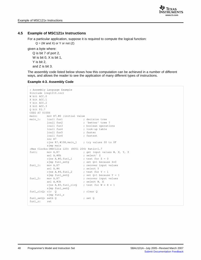
www.ti.com
4.5 Example of MSC121x Instructions
Example of MSC121x Instructions
For a particular application, suppose it is required to compute the logical function:Q = (W and X) or Y or not (Z)
given a byte where:Q is bit 7 of port 2,W is bit 0, X is bit 1,Y is bit 2,and Z is bit 3.
The assembly code listed below shows how this computation can be achieved in a number of differentways, and allows the reader to see the application of many different types of instructions.
Example 4-3. Assembly Code
; Assembly Language Example$include (reg1210.inc)W bit ACC.0X bit ACC.1Y bit ACC.2Z bit ACC.3Q bit P2.7CSEG AT 0100Hmain: mov R7,#0 ;initial valuemain_1: lcall fun1 ; decision tree
lcall fun2 ; 'better' tree ?lcall fun3 ; boolean operationslcall fun4 ; look-up tablelcall fun5 ; fasterlcall fun6 ; fastestinc R7cjne R7,#10H,main_1 ; try values 00 to 0Fsjmp main
;Max Clocks:(MSC121x 120) (8051 204) Ratio=1.7fun1: mov A,R7 ; get input values W, X, Y, Z
anl A,#8h ; select' Zcjne A,#0,fun1_1 ; test for Z = 0sjmp fun1_setQ ; set Q=1 because Z=0
fun1_1: mov A,R7 ; recover input valuesanl A,#4 ; select Ycjne A,#4,fun1_2 ; test for Y = 1sjmp fun1_setQ ; set Q=1 because Y = 1
fun1_2: mov A,R7 ; recover input valuesanl A,#3h ; select W, Xcjne A,#3,fun1_clrQ ; test for W = X = 1sjmp fun1_setQ
fun1_clrQ: clr Q ; clear Qsjmp fun1_z
fun1_setQ: setb Q ; set Qfun1_z: ret
48 Programmer's Model and Instruction Set SBAU101A–July 2005–Revised March 2007Submit Documentation Feedback

www.ti.com
Example of MSC121x Instructions
Example 4-3. Assembly Code (continued)
;Max Clocks:(MSC121x 114) (8051 252) Ratio=2.2fun2: mov A,R7 ; get input values Z,Y,X,W
anl A,#8 ; select Zjz fun2_setQ ; set Q because Z = 0mov A,R7 ; recover inputsanl A,#4 ; select Yjnz fun2_setQ ; set Q because Y = 1mov A,R7 ; recover inputsrrc A ; W into carrymov R0,A ; X in bit #0rlc A ; recover Wanl A,R0 ; AND with Xanl A,#1 ; get just W&Xjnz fun1_setQ ; set Q because W&X = 1clr Q ; Q=0sjmp fun2_z
fun2_setQ: setb Q ; Q=1fun2_z: ret
;Clocks:(MSC121x 60) (8051 144) Ratio=2.4fun3: mov A,R7 ; get input values Z,Y,X,W
mov C,W ; Carry = Wanl C,X ; Carry = W&Xorl C,Y ; Carry = W&X + Yorl C,/Z ; Carry = W&X + Y + /Zmov Q,C ; Output new Q valueret
;Clocks:(MSC121x 64) (8051 120) Ratio=1.9fun4: mov A,R7 ; get input values Z,Y,X,W
anl A,#0FH ; ensure just 4 bitsadd A,#(fun4_t-fun4_1) ; offset for instructionsmovc A,@A+PC ; get table entry
fun4_1: mov C,ACC.0 ; lsb into carrymov Q,C ; and hence Qret
fun4_t: db 1,1,1,1,1,1,1,1 ; table represents easy waydb 0,0,0,1,1,1,1,1 ; to implement any function
;Clocks:(MSC121x 52) (8051 108) Ratio=2.1fun5: mov A,R7 ; get input values Z,Y,X,W
xrl a,#08H ; complement Zclr C ; clear carrysubb A,#3 ; test for boundarycpl C ; correct polaritymov Q,C ; and output to Qret
;Clocks:(MSC121x 44) (8051 84) Ratio=1.9fun6: mov A,R7 ; get input values Z,Y,X,W
xrl A,#08H ; complement Zadd A,#0FDH ; identify boundarymov Q,C ; and output to Qret
end
SBAU101A–July 2005–Revised March 2007 Programmer's Model and Instruction Set 49Submit Documentation Feedback

www.ti.com
Programmer's Model and Instruction Set50 SBAU101A–July 2005–Revised March 2007Submit Documentation Feedback

Chapter 5SBAU101A–July 2005–Revised March 2007
System Clocks, Timers, and Functions
This chapter describes the system clocks, timers, and functions of the MSC121x.
Topic ........................................................................................................... Page
5.1 Timing Chain and Clock Controls ........................................................ 525.2 System Clock Divider (MSC1211/12/13/14)............................................. 545.3 Watchdog Timer................................................................................. 555.4 Low-Voltage Detection........................................................................ 575.5 Hardware Configuration ...................................................................... 585.6 Breakpoints....................................................................................... 60
SBAU101A–July 2005–Revised March 2007 System Clocks, Timers, and Functions 51Submit Documentation Feedback
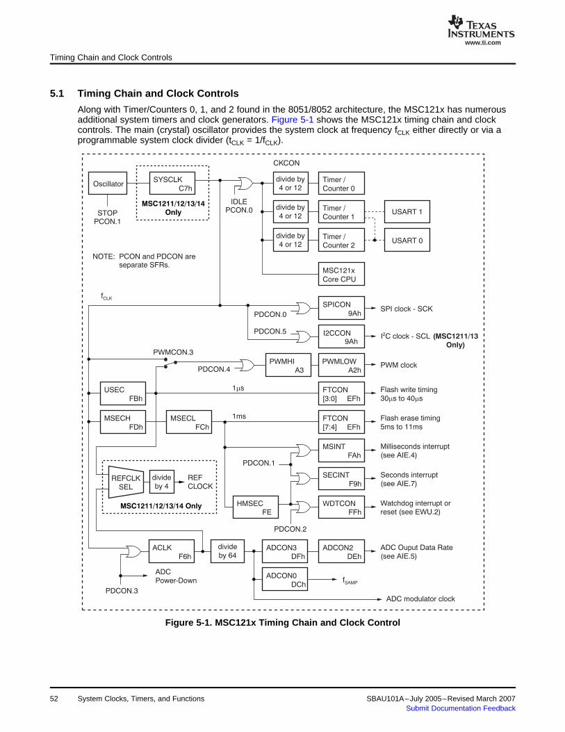
www.ti.com
5.1 Timing Chain and Clock Controls
O cils latordivide by4 or 12
divide by4 or 12
divide by4 or 12
SYSCLK
C7h
Timer /
Counter 0
Timer /Counter 1
Timer /Counter 2
USART 1
USART 0
MSC121x
Core CPU
SPICON
9Ah
I2CCON9Ah
FTCON
[3:0] EFh
MSINT
FAh
SECINT
F9h
WDTCONFFh
ADCON2
DEh
FTCON
[7:4] EFh
MSECL
FCh
MSECH
FDh
HMSECFE
USEC
FBh
PWMHIA3
ACLK
F6h
divideby 64
ADCON3
DFh
ADCON0
DCh
Flash write imingt30ms to 40 sm
Flash era timinse g5ms to 11ms
Milliseconds interrupt(see AIE.4)
Seconds inte ruptr(see AIE.7)
Watchdog interrupt orreset (see EWU.2)
A C Ouput Data RateD(see AIE.5)
SPI clock - SCK
I C cl2 ock - SCL (MSC1211/13Only)
P MLOWWA2h
PWM clock
ADC modulator clock
PDCON.1
PDCON.2
IDLEP ON.0C
PDCON.5
PDCON.0
PDCON.3
ADCPower-Down
MSC1211/12/13/14OnlySTOP
P ON.1C
PDCON.4
PWMCON.3
CKC NO
fCLK
NOTE: PCON and PDCON areseparate SFRs.
1ms
1ms
fSAMP
divideby 4
REFCLOCK
REFCLKSEL
MSC1211/12/13/14 Only
Timing Chain and Clock Controls
Along with Timer/Counters 0, 1, and 2 found in the 8051/8052 architecture, the MSC121x has numerousadditional system timers and clock generators. Figure 5-1 shows the MSC121x timing chain and clockcontrols. The main (crystal) oscillator provides the system clock at frequency fCLK either directly or via aprogrammable system clock divider (tCLK = 1/fCLK).
Figure 5-1. MSC121x Timing Chain and Clock Control
52 System Clocks, Timers, and Functions SBAU101A–July 2005–Revised March 2007Submit Documentation Feedback
www.ti.com
fMOD fCLK
(ACLK 1) 64 (5-1)
ADC Update RatefMOD
Decimation Ratio (5-2)
Timing Chain and Clock Controls
At power-on, or after reset, the signal from the oscillator is not allowed to propagate until after (217 - 1)periods. This period of time allows the power rails and crystal oscillator to stabilize. Thereafter, if neitherPSEN nor ALE is low, the CPU will begin to execute code starting at location 0000h. While operating, theCPU may set bit 1 of PCON at 87h to assert a STOP condition that can only be exited by a hardwarereset. In this condition, all dynamic activity ceases, but the port I/O pins retain their levels. To pause theCPU and core peripherals temporarily, bit 0 may be set. This setting invokes an IDLE state that isterminated by an auxiliary interrupt associated with AIE at A6h, a wake-up via EWU at C6h, or a reset.See Chapter 13 for further detail on interrupts and their sources. PSEN and ALE are used with RESET toenter serial or parallel flash programming modes.
Subsystems are enabled/disabled by bits in PDCON at F1h in any combination, except that SPI and I2Csubsystems must not be simultaneously active. When a bit is high, the associated subsystems are inactiveand power is reduced to a minimum static level.
SPICON [7:5] at 9Ah provides a 3-bit code, N, which selects a tap into a binary divider chain to providethe clock for the SPI interface at a frequency of fCLK/2(N+1).
When the I2C subsystem is active and bit 2 of I2CCON at 9Ah is set, the MSC1211 is in Master mode.The frequency for the I2C clock is then fCLK/2/(I2CSTAT[7:0] + 1).
The external clock input or crystal oscillator provides the system clock either directly, or via aprogrammable divider (MSC1211/12/13/14 only). With a system clock of f MHz, the program must write (f– 1) to the USEC register at FBh in order to provide a clock period as close to 1µs as possible. This clockprovides the start and stop timing for the I2C interface, and is used in conjunction with FTCON [3:0] at EFhto define the Flash memory write cycle timing. The least significant four bits of FTCON are referred to asFWR, and should be set so that (1 + FWR) × (USEC + 1) × 5 × tCLK is between 30µs and 40µs. Thedesigner should consider the relative trade-offs between crystal frequency and accuracy of baud rategeneration versus accuracy of other real-time counters.
By default, the output of the USEC divider is used to clock the PWM generator, but fCLK may be selectedby setting bit 3 of PWMCON at A1h.The operation of the PWM generator is described later.
Just as USEC is programmed to provide a 1µs reference, MSECH at FDh and MSECL at FCh are usedtogether to provide a signal with a period of 1ms to clock other counters. The period is:
(256 × MSECH + MSECL + 1) × tCLK
which may not be an integer number of milliseconds. For example, with a 11.0592MHz crystal andMSECH:MSECL set to 11058, the period will be 1.000018ms. The default value for MSECH:MSECL is3999 and assumes a 4MHz oscillator. Note that if the system divider, defined by SYSCLK at C7h, ispresent and active, an extra division factor may be present as well.
The output of MSECH:MSECL clocks three different counters with reload limits set by FTCON [7:4] atEFh, MSINT [6:0] at FAh, and HMSEC [7:0] at FEh. They define the Flash memory erase timing between5ms and 11ms, the number of counts for the milliseconds interrupt and the hundreds of millisecondinterrupt, respectively. Each counter repeats in N + 1 clocks, where N is the value written to the bits ineach SFR. If bit 7 of MSINT is set, the associated counter will be reloaded as the SFR is written;otherwise, the new value will be loaded next time the count expires.
The interrupt associated with SECINT [6:0] at F9h can be set between 1 and 128 counts of the hundredmillisecond counter. If bit 7 of SECINT is set, the associated counter will be reloaded as the SFR iswritten; otherwise, the new value will be loaded next time the count expires.
The frequency of the ADC modulator is given by:
where ACLK is the SFR at F6h.
The conversion data rate is given by:
The decimation ratio is ADCON3[2:0] at DFh concatenated with ADCON2[7:0] at DEh plus 1, and the ADCoutput data rate is fMOD/(decimation ratio).
SBAU101A–July 2005–Revised March 2007 System Clocks, Timers, and Functions 53Submit Documentation Feedback
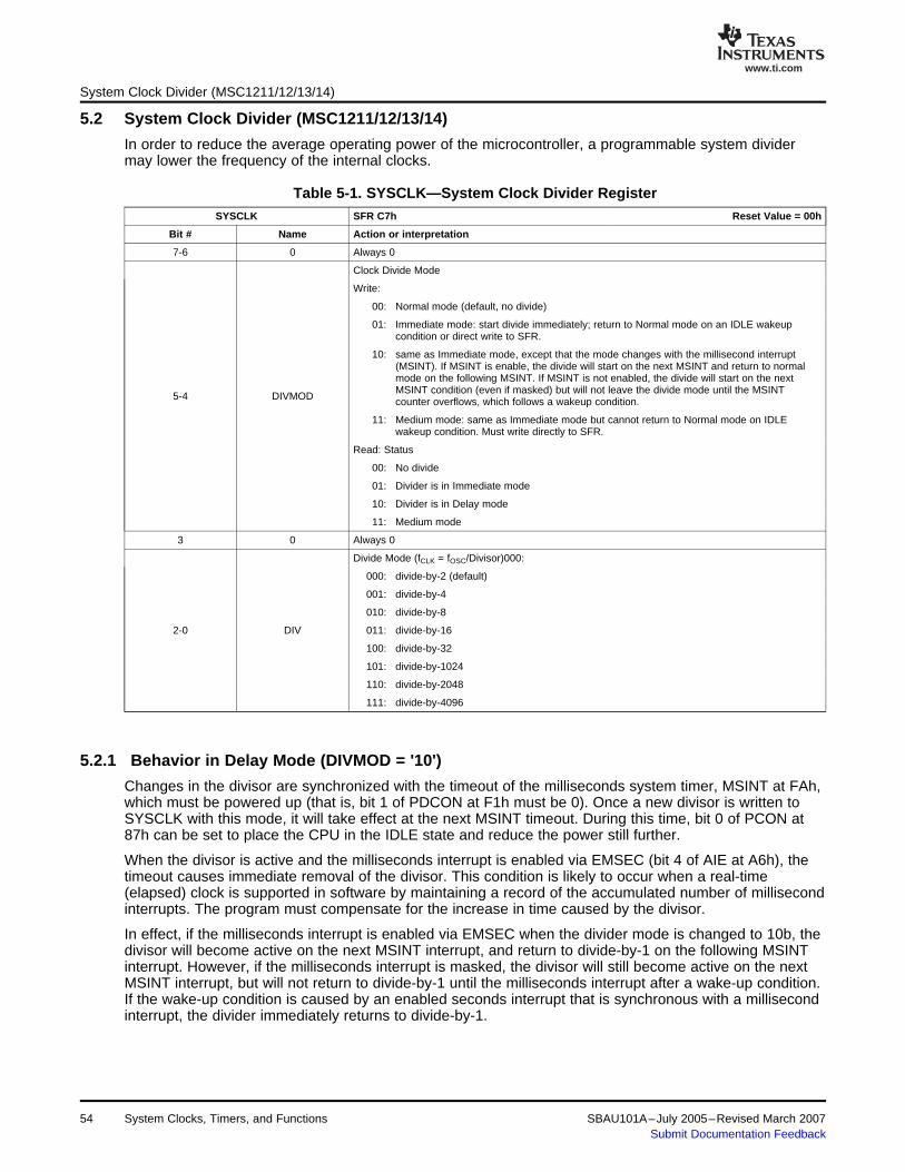
www.ti.com
5.2 System Clock Divider (MSC1211/12/13/14)
5.2.1 Behavior in Delay Mode (DIVMOD = '10')
System Clock Divider (MSC1211/12/13/14)
In order to reduce the average operating power of the microcontroller, a programmable system dividermay lower the frequency of the internal clocks.
Table 5-1. SYSCLK—System Clock Divider RegisterSYSCLK SFR C7h Reset Value = 00h
Bit # Name Action or interpretation
7-6 0 Always 0
Clock Divide Mode
Write:
00: Normal mode (default, no divide)
01: Immediate mode: start divide immediately; return to Normal mode on an IDLE wakeupcondition or direct write to SFR.
10: same as Immediate mode, except that the mode changes with the millisecond interrupt(MSINT). If MSINT is enable, the divide will start on the next MSINT and return to normalmode on the following MSINT. If MSINT is not enabled, the divide will start on the nextMSINT condition (even if masked) but will not leave the divide mode until the MSINT
5-4 DIVMOD counter overflows, which follows a wakeup condition.
11: Medium mode: same as Immediate mode but cannot return to Normal mode on IDLEwakeup condition. Must write directly to SFR.
Read: Status
00: No divide
01: Divider is in Immediate mode
10: Divider is in Delay mode
11: Medium mode
3 0 Always 0
Divide Mode (fCLK = fOSC/Divisor)000:
000: divide-by-2 (default)
001: divide-by-4
010: divide-by-8
2-0 DIV 011: divide-by-16
100: divide-by-32
101: divide-by-1024
110: divide-by-2048
111: divide-by-4096
Changes in the divisor are synchronized with the timeout of the milliseconds system timer, MSINT at FAh,which must be powered up (that is, bit 1 of PDCON at F1h must be 0). Once a new divisor is written toSYSCLK with this mode, it will take effect at the next MSINT timeout. During this time, bit 0 of PCON at87h can be set to place the CPU in the IDLE state and reduce the power still further.
When the divisor is active and the milliseconds interrupt is enabled via EMSEC (bit 4 of AIE at A6h), thetimeout causes immediate removal of the divisor. This condition is likely to occur when a real-time(elapsed) clock is supported in software by maintaining a record of the accumulated number of millisecondinterrupts. The program must compensate for the increase in time caused by the divisor.
In effect, if the milliseconds interrupt is enabled via EMSEC when the divider mode is changed to 10b, thedivisor will become active on the next MSINT interrupt, and return to divide-by-1 on the following MSINTinterrupt. However, if the milliseconds interrupt is masked, the divisor will still become active on the nextMSINT interrupt, but will not return to divide-by-1 until the milliseconds interrupt after a wake-up condition.If the wake-up condition is caused by an enabled seconds interrupt that is synchronous with a millisecondinterrupt, the divider immediately returns to divide-by-1.
54 System Clocks, Timers, and Functions SBAU101A–July 2005–Revised March 2007Submit Documentation Feedback

www.ti.com
5.3 Watchdog Timer
Watchdog Timer
WDTCON [4:0] at FFh plus 1 defines the number of 100ms intervals before the watchdog timer expires,assuming that the watchdog restart sequence is not performed. The watchdog is enabled (or disabled) bywriting a 1,0 sequence to bit 7 (or bit 6) of WDTCON. Writing 1,0 to bit 5 restarts the timeout.
When the watchdog is enabled and expires, it generates either an interrupt or a reset (default), asdetermined by bit 3 of HCR0.
WDTI must be cleared within the interrupt service routine (ISR). Setting WDTI in software generates awatchdog timer interrupt, if enabled.
Table 5-2. Watchdog Control BitsWatchdog Interrupt has priority 12 (Low) and jumps to address 63h
Bit Name Abbreviation Name of Related SFR Abbreviation Address (Hex)
Global Interrupt Enable EA Interrupt Enable IE.7 A8
Enable Watchdog Interrupt EWDI Extended Interrupt Enable EIE.4 E8
Watchdog Timer Interrupt flag WDTI Enable Interrupt Control EICON.3 D8
Watchdog Interrupt Priority PWDI Extended Interrupt Priority EIP.4 F8
SBAU101A–July 2005–Revised March 2007 System Clocks, Timers, and Functions 55Submit Documentation Feedback

www.ti.com
5.3.1 Watchdog Timer Example Program
Watchdog Timer
When the program is run, it first requires a carriage return (CR) character to be received so that the baudrate can be determined. Thereafter, a CR code must be repeatedly received within three seconds;otherwise, the MSC121x is reset and the autobaud routine is restarted.
In Example 5-1, EWDR, bit 3 of HCR0, must be 1 (default) for a reset to occur. In another application, theprogrammer may clear EWDR so that when the timer expires, an interrupt is requested via WDTI, bit 3 ofEICON at D8h.
Example 5-1. Watchdog Timer Program
// File WDT.c - Watch Dog Timer// MSC1210 EVM Switches 1:On SW3-12345678 SW6-12345678// 0:Off 11110111 11110000#include <Reg1210.h>#include <stdio.h>#define xtal 11059200sbit RedLed = P3^4; // RED LED on EVMsbit YellowLed = P3^5; // Yellow LED on EVMcode at 0xFFF3 void autobaud(void);
data unsigned char i='A';
void main(void) PDCON&=~0x04; // power up WatchDogMSEC=xtal/1000-1; // 1ms tickHMSEC=100-1; // 100ms tickRedLed=0; // Turn Red LED onautobaud(); // Requires CRprintf("\nMSC1210 Watchdog Test");printf("\nRepeatedly press CR/Enter within 3 seconds\n");RI_0 = 0; // clear received flag in USARTWDTCON=0x80; // start watchdog and defineWDTCON=30; // 30 * 100ms timeoutRedLed=1; // Turn Red LED offwhile(1)while(!RI_0); // wait for key pressYellowLed=!YellowLed; // Toggle Yellow Ledputchar(i);i=(i+1) & 0x5F; // 32 character sequenceif((SBUF0 & 0x7F)==0x0D) // Test for CR
WDTCON|=0x20; // restart Watchdog timerWDTCON&=~0x20; // with 1-0 sequence in bit #5
RI_0 = 0; // clear received flag in USART
56 System Clocks, Timers, and Functions SBAU101A–July 2005–Revised March 2007Submit Documentation Feedback
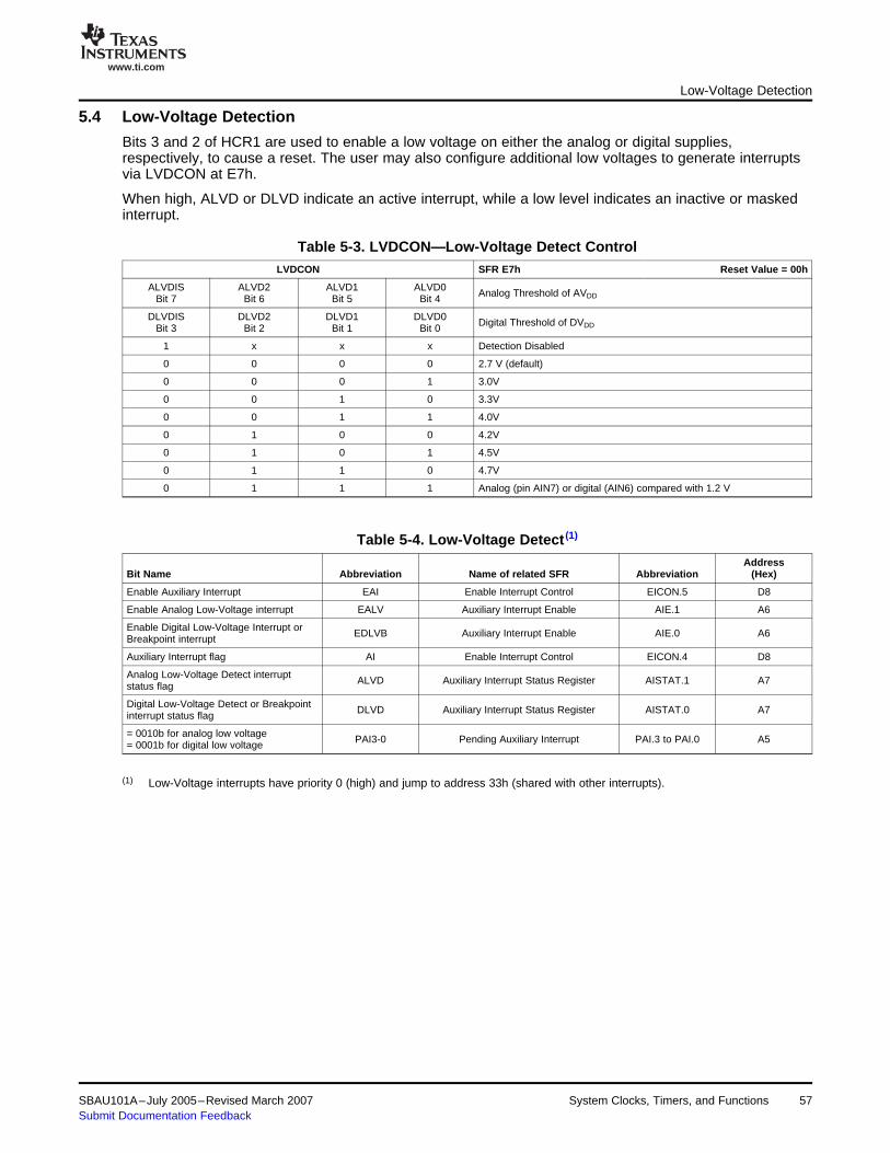
www.ti.com
5.4 Low-Voltage Detection
Low-Voltage Detection
Bits 3 and 2 of HCR1 are used to enable a low voltage on either the analog or digital supplies,respectively, to cause a reset. The user may also configure additional low voltages to generate interruptsvia LVDCON at E7h.
When high, ALVD or DLVD indicate an active interrupt, while a low level indicates an inactive or maskedinterrupt.
Table 5-3. LVDCON—Low-Voltage Detect ControlLVDCON SFR E7h Reset Value = 00h
ALVDIS ALVD2 ALVD1 ALVD0 Analog Threshold of AVDDBit 7 Bit 6 Bit 5 Bit 4
DLVDIS DLVD2 DLVD1 DLVD0 Digital Threshold of DVDDBit 3 Bit 2 Bit 1 Bit 0
1 x x x Detection Disabled
0 0 0 0 2.7 V (default)
0 0 0 1 3.0V
0 0 1 0 3.3V
0 0 1 1 4.0V
0 1 0 0 4.2V
0 1 0 1 4.5V
0 1 1 0 4.7V
0 1 1 1 Analog (pin AIN7) or digital (AIN6) compared with 1.2 V
Table 5-4. Low-Voltage Detect (1)
AddressBit Name Abbreviation Name of related SFR Abbreviation (Hex)
Enable Auxiliary Interrupt EAI Enable Interrupt Control EICON.5 D8
Enable Analog Low-Voltage interrupt EALV Auxiliary Interrupt Enable AIE.1 A6
Enable Digital Low-Voltage Interrupt or EDLVB Auxiliary Interrupt Enable AIE.0 A6Breakpoint interrupt
Auxiliary Interrupt flag AI Enable Interrupt Control EICON.4 D8
Analog Low-Voltage Detect interrupt ALVD Auxiliary Interrupt Status Register AISTAT.1 A7status flag
Digital Low-Voltage Detect or Breakpoint DLVD Auxiliary Interrupt Status Register AISTAT.0 A7interrupt status flag
= 0010b for analog low voltage PAI3-0 Pending Auxiliary Interrupt PAI.3 to PAI.0 A5= 0001b for digital low voltage
(1) Low-Voltage interrupts have priority 0 (high) and jump to address 33h (shared with other interrupts).
SBAU101A–July 2005–Revised March 2007 System Clocks, Timers, and Functions 57Submit Documentation Feedback
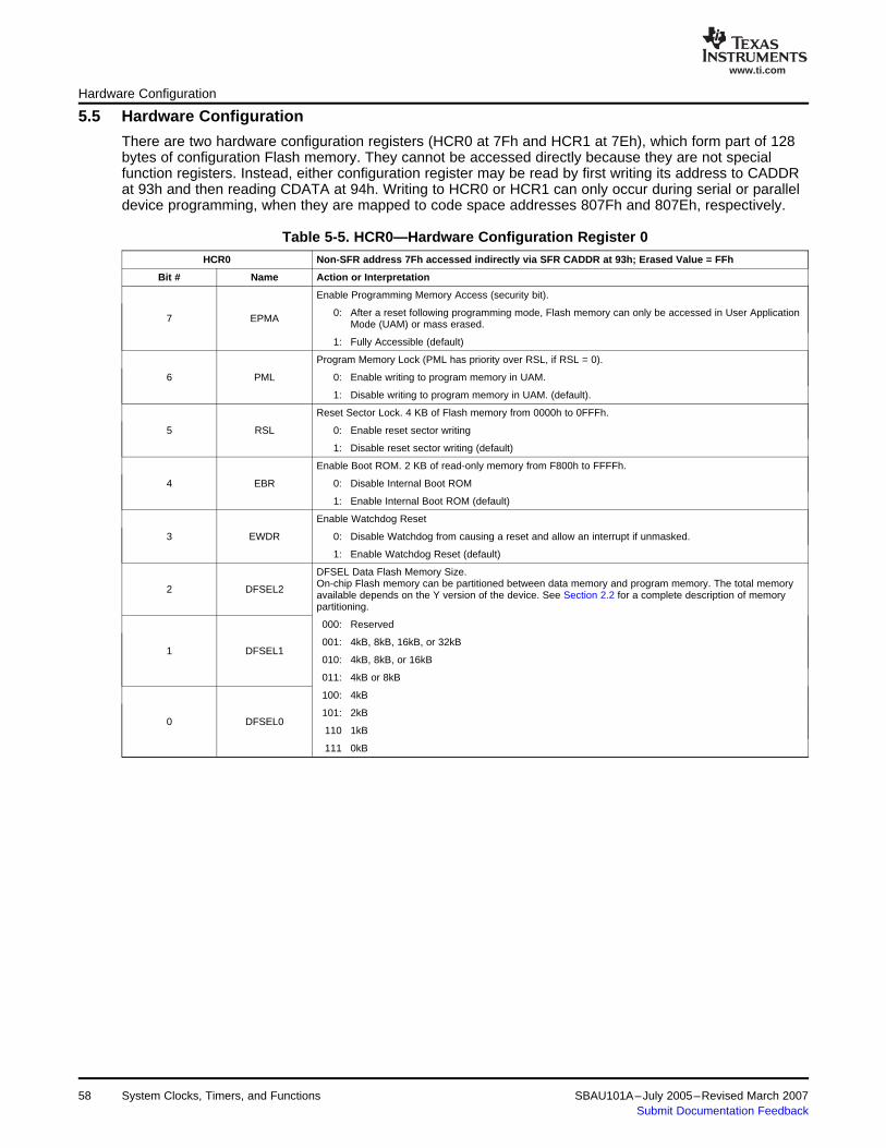
www.ti.com
5.5 Hardware ConfigurationHardware Configuration
There are two hardware configuration registers (HCR0 at 7Fh and HCR1 at 7Eh), which form part of 128bytes of configuration Flash memory. They cannot be accessed directly because they are not specialfunction registers. Instead, either configuration register may be read by first writing its address to CADDRat 93h and then reading CDATA at 94h. Writing to HCR0 or HCR1 can only occur during serial or paralleldevice programming, when they are mapped to code space addresses 807Fh and 807Eh, respectively.
Table 5-5. HCR0—Hardware Configuration Register 0HCR0 Non-SFR address 7Fh accessed indirectly via SFR CADDR at 93h; Erased Value = FFh
Bit # Name Action or Interpretation
Enable Programming Memory Access (security bit).
0: After a reset following programming mode, Flash memory can only be accessed in User Application7 EPMA Mode (UAM) or mass erased.
1: Fully Accessible (default)
Program Memory Lock (PML has priority over RSL, if RSL = 0).
6 PML 0: Enable writing to program memory in UAM.
1: Disable writing to program memory in UAM. (default).
Reset Sector Lock. 4 KB of Flash memory from 0000h to 0FFFh.
5 RSL 0: Enable reset sector writing
1: Disable reset sector writing (default)
Enable Boot ROM. 2 KB of read-only memory from F800h to FFFFh.
4 EBR 0: Disable Internal Boot ROM
1: Enable Internal Boot ROM (default)
Enable Watchdog Reset
3 EWDR 0: Disable Watchdog from causing a reset and allow an interrupt if unmasked.
1: Enable Watchdog Reset (default)
DFSEL Data Flash Memory Size.On-chip Flash memory can be partitioned between data memory and program memory. The total memory2 DFSEL2 available depends on the Y version of the device. See Section 2.2 for a complete description of memorypartitioning.
000: Reserved
001: 4kB, 8kB, 16kB, or 32kB1 DFSEL1
010: 4kB, 8kB, or 16kB
011: 4kB or 8kB
100: 4kB
101: 2kB0 DFSEL0
110 1kB
111 0kB
58 System Clocks, Timers, and Functions SBAU101A–July 2005–Revised March 2007Submit Documentation Feedback
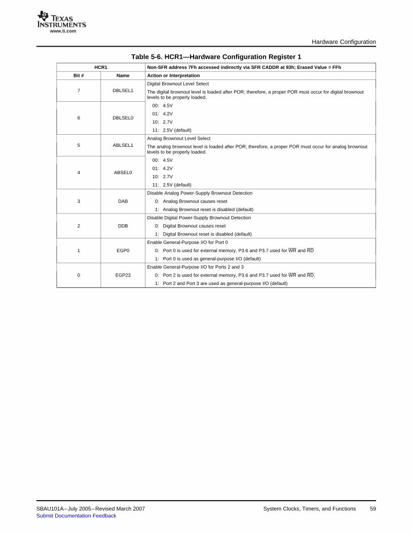
www.ti.com
Hardware Configuration
Table 5-6. HCR1—Hardware Configuration Register 1HCR1 Non-SFR address 7Fh accessed indirectly via SFR CADDR at 93h; Erased Value = FFh
Bit # Name Action or Interpretation
Digital Brownout Level Select7 DBLSEL1 The digital brownout level is loaded after POR; therefore, a proper POR must occur for digital brownout
levels to be properly loaded.
00: 4.5V
01: 4.2V6 DBLSEL0
10: 2.7V
11: 2.5V (default)
Analog Brownout Level Select5 ABLSEL1 The analog brownout level is loaded after POR; therefore, a proper POR must occur for analog brownout
levels to be properly loaded.
00: 4.5V
01: 4.2V4 ABSEL0
10: 2.7V
11: 2.5V (default)
Disable Analog Power-Supply Brownout Detection
3 DAB 0: Analog Brownout causes reset
1: Analog Brownout reset is disabled (default)
Disable Digital Power-Supply Brownout Detection
2 DDB 0: Digital Brownout causes reset
1: Digital Brownout reset is disabled (default)
Enable General-Purpose I/O for Port 0
1 EGP0 0: Port 0 is used for external memory, P3.6 and P3.7 used for WR and RD
1: Port 0 is used as general-purpose I/O (default)
Enable General-Purpose I/O for Ports 2 and 3
0 EGP23 0: Port 2 is used for external memory, P3.6 and P3.7 used for WR and RD.
1: Port 2 and Port 3 are used as general-purpose I/O (default)
SBAU101A–July 2005–Revised March 2007 System Clocks, Timers, and Functions 59Submit Documentation Feedback
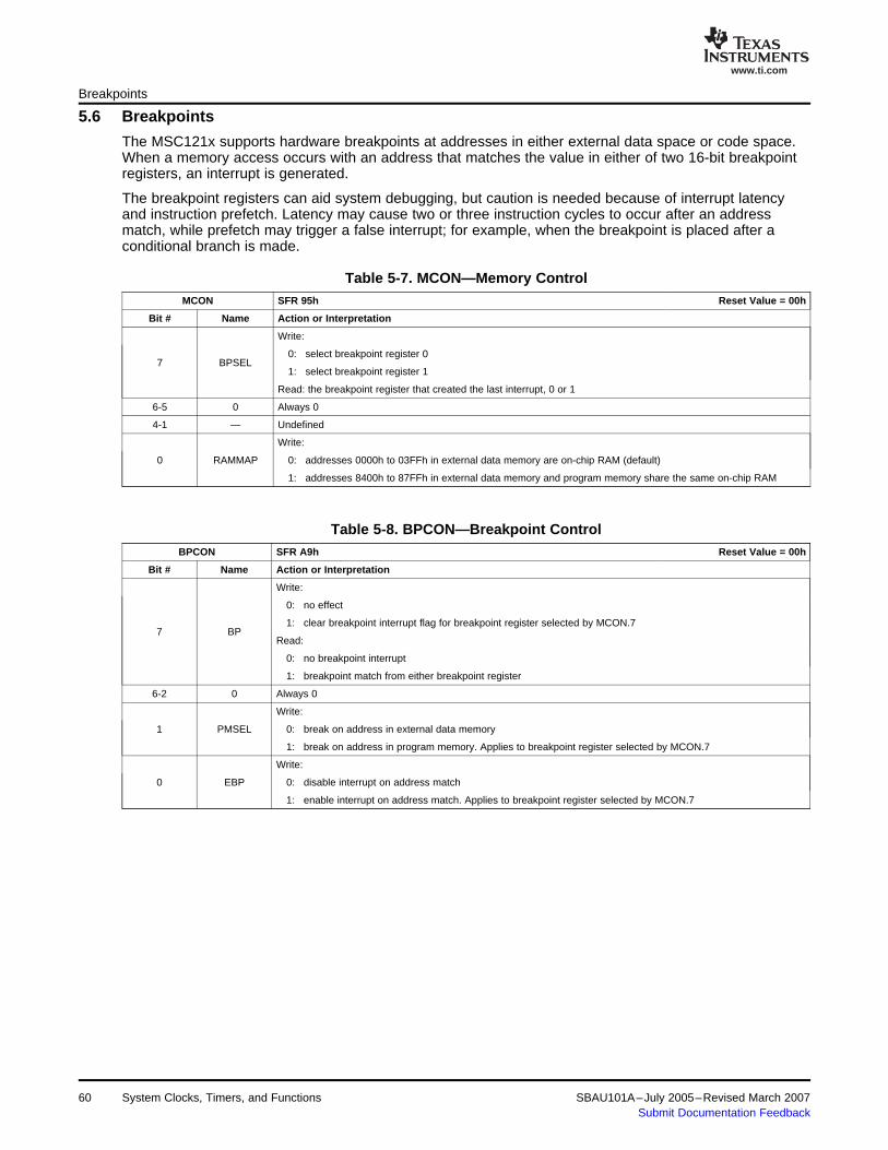
www.ti.com
5.6 BreakpointsBreakpoints
The MSC121x supports hardware breakpoints at addresses in either external data space or code space.When a memory access occurs with an address that matches the value in either of two 16-bit breakpointregisters, an interrupt is generated.
The breakpoint registers can aid system debugging, but caution is needed because of interrupt latencyand instruction prefetch. Latency may cause two or three instruction cycles to occur after an addressmatch, while prefetch may trigger a false interrupt; for example, when the breakpoint is placed after aconditional branch is made.
Table 5-7. MCON—Memory ControlMCON SFR 95h Reset Value = 00h
Bit # Name Action or Interpretation
Write:
0: select breakpoint register 07 BPSEL
1: select breakpoint register 1
Read: the breakpoint register that created the last interrupt, 0 or 1
6-5 0 Always 0
4-1 — Undefined
Write:
0 RAMMAP 0: addresses 0000h to 03FFh in external data memory are on-chip RAM (default)
1: addresses 8400h to 87FFh in external data memory and program memory share the same on-chip RAM
Table 5-8. BPCON—Breakpoint ControlBPCON SFR A9h Reset Value = 00h
Bit # Name Action or Interpretation
Write:
0: no effect
1: clear breakpoint interrupt flag for breakpoint register selected by MCON.77 BP
Read:
0: no breakpoint interrupt
1: breakpoint match from either breakpoint register
6-2 0 Always 0
Write:
1 PMSEL 0: break on address in external data memory
1: break on address in program memory. Applies to breakpoint register selected by MCON.7
Write:
0 EBP 0: disable interrupt on address match
1: enable interrupt on address match. Applies to breakpoint register selected by MCON.7
60 System Clocks, Timers, and Functions SBAU101A–July 2005–Revised March 2007Submit Documentation Feedback
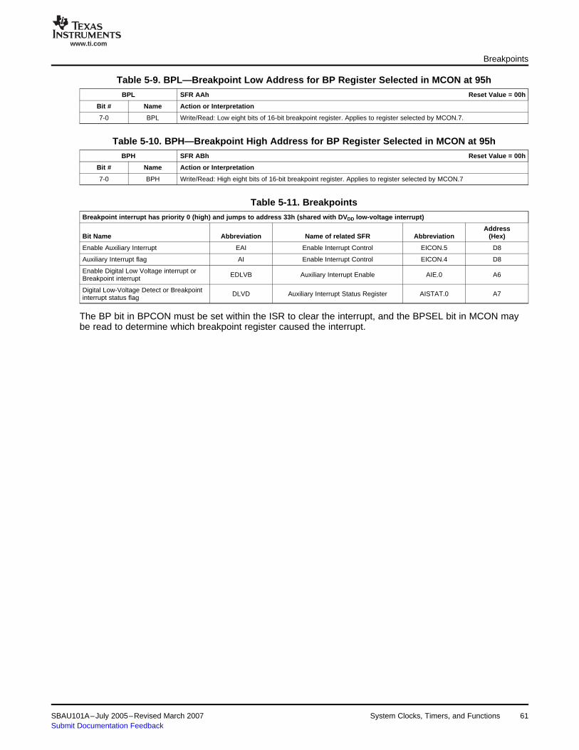
www.ti.com
Breakpoints
Table 5-9. BPL—Breakpoint Low Address for BP Register Selected in MCON at 95hBPL SFR AAh Reset Value = 00h
Bit # Name Action or Interpretation
7-0 BPL Write/Read: Low eight bits of 16-bit breakpoint register. Applies to register selected by MCON.7.
Table 5-10. BPH—Breakpoint High Address for BP Register Selected in MCON at 95hBPH SFR ABh Reset Value = 00h
Bit # Name Action or Interpretation
7-0 BPH Write/Read: High eight bits of 16-bit breakpoint register. Applies to register selected by MCON.7
Table 5-11. BreakpointsBreakpoint interrupt has priority 0 (high) and jumps to address 33h (shared with DVDD low-voltage interrupt)
AddressBit Name Abbreviation Name of related SFR Abbreviation (Hex)
Enable Auxiliary Interrupt EAI Enable Interrupt Control EICON.5 D8
Auxiliary Interrupt flag AI Enable Interrupt Control EICON.4 D8
Enable Digital Low Voltage interrupt or EDLVB Auxiliary Interrupt Enable AIE.0 A6Breakpoint interrupt
Digital Low-Voltage Detect or Breakpoint DLVD Auxiliary Interrupt Status Register AISTAT.0 A7interrupt status flag
The BP bit in BPCON must be set within the ISR to clear the interrupt, and the BPSEL bit in MCON maybe read to determine which breakpoint register caused the interrupt.
SBAU101A–July 2005–Revised March 2007 System Clocks, Timers, and Functions 61Submit Documentation Feedback

www.ti.com
System Clocks, Timers, and Functions62 SBAU101A–July 2005–Revised March 2007Submit Documentation Feedback
Chapter 6SBAU101A–July 2005–Revised March 2007
Analog-To-Digital Converters
This chapter describes the analog-to-digital converters (ADCs) of the MSC121x.
Topic ........................................................................................................... Page
6.1 ADC Functional Blocks....................................................................... 646.2 ADC Signal Flow and General Description ............................................ 656.3 Analog Input Stage............................................................................. 656.4 Input Impedance, PGA, and Voltage References .................................... 676.5 Offset DAC ........................................................................................ 696.6 ADC Data Rate, Filters, and Calibration ................................................ 706.7 32-Bit Summation Register.................................................................. 726.8 Accessing the ADC Multi-Byte Conversion in C ..................................... 746.9 ADC Example Program ....................................................................... 75
SBAU101A–July 2005–Revised March 2007 Analog-To-Digital Converters 63Submit Documentation Feedback

www.ti.com
6.1 ADC Functional Blocks
Σ
Σ X
InputMultiplexer
TemperatureSensor
Buffer PGASample
and Hold
ADMUXD7h
REFOUT/REF IN+
REF IN−
REFOUT/REF IN+ fMOD
REF IN−
AIN5AIN6AIN7
AINCOM
ADCON1DDh
ADCON2DEh
ADCON3DFh
OCR GCR ADRES
SUMR
D3h D2h D1h D6h D5h D4h DBh DAh D9h
E5h E4h E3h E2h
OffsetCalibrationRegister
ADC0N0DCh ACLKF6h
SSCONE1h
ODACE6h
OffsetDAC
∆Σ ADCModulator
FAST
SINC2SINC3
AUTO
ADCResult Register
Σ
SummationBlock
VIN
AIN2AIN3AIN4
AIN0AIN1
fSAMP
fDATA
GainCalibrationRegister
BurnoutDetect
AVDD
In+
AGND
In−
BurnoutDetect
ADC Functional Blocks
A key feature of the MSC121x that differentiates it from other mixed-signal microcontrollers is ahigh-precision analog-to-digital subsystem, with a performance that is usually found only in embeddedsystems with a separate ADC and microprocessor. The major elements of the ADC subsystem are shownin Figure 6-1.
Figure 6-1. ADC Subsystem Elements
64 Analog-To-Digital Converters SBAU101A–July 2005–Revised March 2007Submit Documentation Feedback

www.ti.com
6.2 ADC Signal Flow and General Description
6.3 Analog Input Stage
Vnk ln(80)
q (TC 273.16) TC
ADC Signal Flow and General Description
Analog signals from pins AIN0 to AIN7, AINCOM, or internal temperature-sensitive diodes are selectedindependently by two analog multiplexers to provide a differential signal to the programmable gainamplifier (PGA), which may optionally be preceded by a high-impedance buffer. An analog offset of up to±50% of the full range may be injected into the PGA by the Offset DAC.
The delta-sigma (∆Σ) ADC can be configured for sampling rate and decimation ratio as well as filter typebefore its output is passed to digital offset and gain calibration stages to give a 24-bit unipolar or bipolarresult.
ADC conversions can be automatically added to a 32-bit summation register (SUMR3 to SUMR0), whichis considerably more efficient than using machine-code instructions. A defined number of conversions mayalso trigger an automatic right shift to produce an averaged value. The CPU can control the 32-bithardware accumulator directly, as long as the ADC subsystem is powered up. All MSC121x family partsexcept for the MSC1210 also support 32-bit subtraction.
Special function register ADMUX at D7h provides two groups of four bits each that specify the analogsource channels for the noninverting (positive) and inverting (negative) inputs to the buffer and/or thePGA.
The upper four bits control the noninverting input while the lower four bits control the inverting input.Codes 0000b to 0111b represent channels AIN0 to AIN7, respectively. Code 1000b selects AINCOM, andif both codes are 1111b, two temperature-sensitive diodes are selected.
When Burnout Detection is enabled, current sources cause the inputs to be pulled to either AVDD orAGND if the selected channel is open circuit, as may happen when a resistive sensor is broken.
The internal diodes are used to provide a temperature-sensitive differential voltage of approximately:
For typical values of α (temperature sensor coefficient) and β (temperature sensor voltage) , refer to theElectrical Characteristics section of the respective datasheet.
For further information about accuracy and calibration, see Texas Instruments application reportSBAA100, Using the MSC121x as a High-Precision Intelligent Temperature Sensor, available fordownload at www.ti.com.
SBAU101A–July 2005–Revised March 2007 Analog-To-Digital Converters 65Submit Documentation Feedback
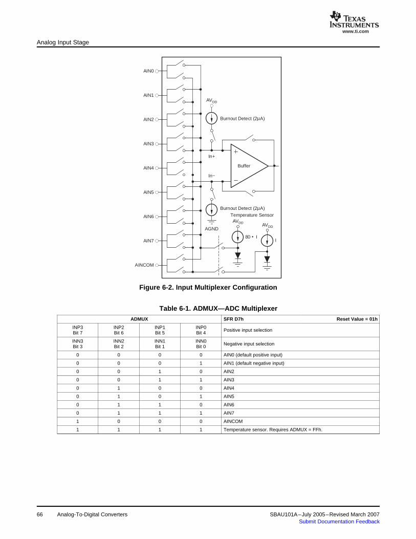
www.ti.com
AIN3
AIN4
AIN5
AIN6
AIN0
AIN1
AIN2
AIN7
AINCOM
Burnout Detect (2µA)
Burnout Detect (2µA)
AGND
Buffer
Temperature Sensor
I80 • I
AVDD
AVDD AVDD
In+
In−
Analog Input Stage
Figure 6-2. Input Multiplexer Configuration
Table 6-1. ADMUX—ADC MultiplexerADMUX SFR D7h Reset Value = 01h
INP3 INP2 INP1 INP0 Positive input selectionBit 7 Bit 6 Bit 5 Bit 4
INN3 INN2 INN1 INN0 Negative input selectionBit 3 Bit 2 Bit 1 Bit 0
0 0 0 0 AIN0 (default positive input)
0 0 0 1 AIN1 (default negative input)
0 0 1 0 AIN2
0 0 1 1 AIN3
0 1 0 0 AIN4
0 1 0 1 AIN5
0 1 1 0 AIN6
0 1 1 1 AIN7
1 0 0 0 AINCOM
1 1 1 1 Temperature sensor. Requires ADMUX = FFh.
66 Analog-To-Digital Converters SBAU101A–July 2005–Revised March 2007Submit Documentation Feedback
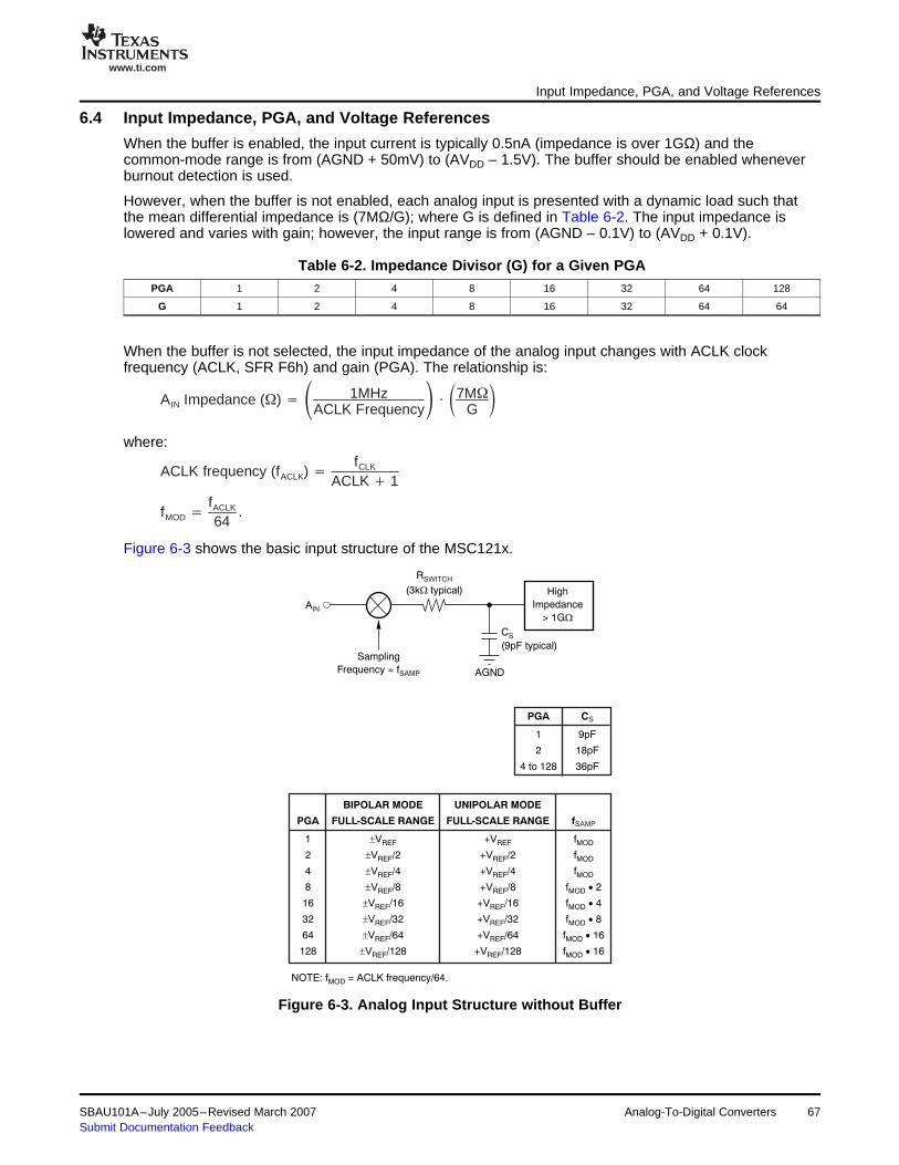
www.ti.com
6.4 Input Impedance, PGA, and Voltage References
A IN Impedance () 1MHzACLK Frequency
7MG
ACLK frequency (fACLK)fCLK
ACLK 1
fMODfACLK
64.
RSWITCH
(3k typical)W
Sampling
Frequency = fSAMP
High
Impedance
> 1GW
AGND
AIN
CS
(9pF typical)
PGA
1
2
4 to 128
C
9pF
18pF
36pF
S
PGA
1
2
4
8
16
32
64
128
f
f
f
f
f 2
f 4
f 8
f 16
f 16
MOD
MOD
MOD
MOD
MOD
MOD
MOD
MOD
·
·
·
·
·
SAMP
BIPOLAR MODE
FULL-SCALE RANGE
±V
V /2
V /4
V /8
V /16
V /32
V /64
V /128
REF
REF
REF
REF
REF
REF
REF
REF
±
±
±
±
±
±
±
UNIPOLAR MODE
FULL-SCALE RANGE
+V
+V /2
+V /4
+V /8
+V /16
+V /32
+V /64
+V /128
REF
REF
REF
REF
REF
REF
REF
REF
NOTE: f = ACLK frequency/64.MOD
Input Impedance, PGA, and Voltage References
When the buffer is enabled, the input current is typically 0.5nA (impedance is over 1GΩ) and thecommon-mode range is from (AGND + 50mV) to (AVDD – 1.5V). The buffer should be enabled wheneverburnout detection is used.
However, when the buffer is not enabled, each analog input is presented with a dynamic load such thatthe mean differential impedance is (7MΩ/G); where G is defined in Table 6-2. The input impedance islowered and varies with gain; however, the input range is from (AGND – 0.1V) to (AVDD + 0.1V).
Table 6-2. Impedance Divisor (G) for a Given PGAPGA 1 2 4 8 16 32 64 128
G 1 2 4 8 16 32 64 64
When the buffer is not selected, the input impedance of the analog input changes with ACLK clockfrequency (ACLK, SFR F6h) and gain (PGA). The relationship is:
where:
Figure 6-3 shows the basic input structure of the MSC121x.
Figure 6-3. Analog Input Structure without Buffer
SBAU101A–July 2005–Revised March 2007 Analog-To-Digital Converters 67Submit Documentation Feedback

www.ti.com
tCLK(ACLK 1) 4
USEC4
Input Impedance, PGA, and Voltage References
Table 6-3. ADCON0—ADC Control Register 0ADCON0 SFR DCh Reset Value = 30h
Bit # Name Action or Interpretation
Reference Clock (MSC1211/12/13/14 only)
The reference is specified with a 250kHz clock. REFCLK should be selected by choosing the appropriate source sothat it does not exceed 250kHz.
0:7 REFCLK
1:
Burnout Detect
When enabled, a 2µA current source is connected from AVDD to the positive input, while a 2µA current sink isconnected from the negative input to ground.
6 BOD Write:
0: Burnout Current Sources Off (default)
1: Burnout Current Sources On
Enable Internal Voltage Reference
Write:5 EVREF 0: Internal Voltage Reference Off
1: Internal Voltage Reference On (default). If the internal voltage reference is not used, it should be turned off tosave power and reduce noise
Voltage Reference High Select
Write:4 VREFH
0: REFOUT is 1.25V
1: REFOUT is 2.5V (default)
Enable Buffer
Write:3 EBUF
Buffer disabled (default)
Buffer enabled, results in increased power and impedance but reduced range
Programmable Gain Amplifier
Write:2-0 PGA
000 to 111: Gives a gain
G = 2PGA or 1 (default) to 128
PGA Bits of ADCON0 determine various parameters according to Table 6-4.
Table 6-4. ADCON0 PGA Bit ParametersPGA Effective Number RMS ResolutionBits Full-Scale Sampling of Bits for VREF = 2.5V[2:0] Gain Range Frequency at 10Hz Rate (nV)
000 1 ±VREF fMOD 21.7 1468
001 2 ±VREF/2 fMOD 21.5 843
010 4 ±VREF/4 fMOD 21.4 452
011 8 ±VREF/8 2 fMOD 21.2 259
100 16 ±VREF/16 4 fMOD 20.8 171
101 32 ±VREF/32 8 fMOD 20.4 113
110 64 ±VREF/64 16 fMOD 20 74.5
111 128 ±VREF/128 16 fMOD 19 74.5
Analog-To-Digital Converters68 SBAU101A–July 2005–Revised March 2007Submit Documentation Feedback

www.ti.com
6.5 Offset DAC
Offset VREF
2PGAODAC[6 : 0]
127( 1) [ODAC7]
Offset DAC
By default, the internal voltage reference is turned on at 2.5V, when the ADC subsystem is powered up.Therefore, if an external reference is provided, the internal reference should be disabled via EVREFbefore bit 3 of PDCON at F1h is cleared.
If the internal voltage reference is to be used, the default level of 2.5V is allowed only if AVDD is between3.3V and 5.25V. The internal 1.25V VREF can be used over the entire analog supply range (AVDD = 2.7V to5.25V).
When the internal voltage reference is disabled, an external differential reference is represented by thevoltage between REF IN+ and REF IN–. This permits ratiometric measurements, but the absolute voltageon either input must be from AGND to AVDD.
In both cases, the REF IN+ pin should have a 0.1µF capacitor to AGND.
The PGA input range may be offset by up to ±50% via the offset DAC. This 8-bit DAC is controlled byODAC at E6h with a coding scheme such that the most significant bit represents the sign of the offset,while the least significant seven bits represent the magnitude. When the magnitude is zero, the ODAC isdisabled and the voltage into the PGA is not offset.
where PGA is the gain of the programmable gain amplifier.
Here, VREF is the voltage on the REF IN+ pin with respect to REF IN– and should not be confused with theinternal voltage reference that is with respect to AGND.
The gain error of the 8-bit ODAC is typically about ±1.5% of its range, which means its absolute accuracycan be significant in some applications. However, it is monotonic with an integral nonlinearity of less than0.25 bits, and has a temperature coefficient of typically 1ppm/°C. It may be used in a predictive mannerwith due regard to its range, resolution, stability, and accuracy, or it may be calibrated using the ADC.
SBAU101A–July 2005–Revised March 2007 Analog-To-Digital Converters 69Submit Documentation Feedback
www.ti.com
6.6 ADC Data Rate, Filters, and Calibration
ADC Output Data Rate fDATAfMOD
Decimation Ratio
1tDATA
where fMOD fCLK
(ACLK 1) 64
ADC Data Rate, Filters, and Calibration
The data rate for ADC conversions is determined by the frequency of the modulator clock, fMOD, and thedecimation ratio, which is a right-justified, 11-bit field in ADCON3 at DFh (high) concatenated withADCON2 at DEh (low). The default data rate is 1563.
When the decimation ratio, PGA, AVDD, or temperature are changed, the ADC must be recalibrated.
The mode of operation of the ADC is controlled by ADCON1 at DDh, which determines whether the inputsare interpreted as unipolar or bipolar, the type of digital filter, and the type of calibration.
Table 6-5. ADCON1—ADC Control Register 1ADCON1 SFR DDh Reset Value = 30h
Bit # Name Action or Interpretation
Summation Invalid7 OF_UF If this bit is set, the data in the summation register is invalid; either an overflow or underflow occurred. The bit is cleared
by writing a '0' to it.
Polarity
Write:6 POL
0: Bipolar such that –FSR = 0x800000, zero = 0x000000 and +FSR = 0x7FFFFF
1: Unipolar such that –FSR = 0x000000, zero = 0x000000 and +FSR = 0xFFFFFF
Settling Mode
5 SM1 Write:
00: Auto
01: Fast
10:4 SM0 Sinc2
11: Sinc3
3 — Not used
Calibration Control (number of tDATA periods to complete)
Write:2 CAL2
000: No Calibration (default)
001: Self Calibration for Offset and Gain (14)
010: Self Calibration for Offset only (7)
011: Self Calibration for Gain only (7)1 CAL1
100: System Calibration for Offset only (7)
101: System Calibration for Gain only (7)
110: Reserved
111: Reserved0 CAL0
Read:
000
When the voltage presented to the ADC changes, the time it takes to receive valid data depends upon thetype of filter that is selected, as well as the conversion time, tDATA. Higher-order filters provide better noiseimmunity but take longer to settle, and the user must make considered judgments as to systemperformance based on resolution, settling time, and notch frequency.
In Auto mode, the type of filter that is used changes whenever the input multiplexer, ADMUX, or PGA arealtered. The ADC first makes two conversions using the Fast filter, then one with Sinc2, and then one withSinc3.
70 Analog-To-Digital Converters SBAU101A–July 2005–Revised March 2007Submit Documentation Feedback
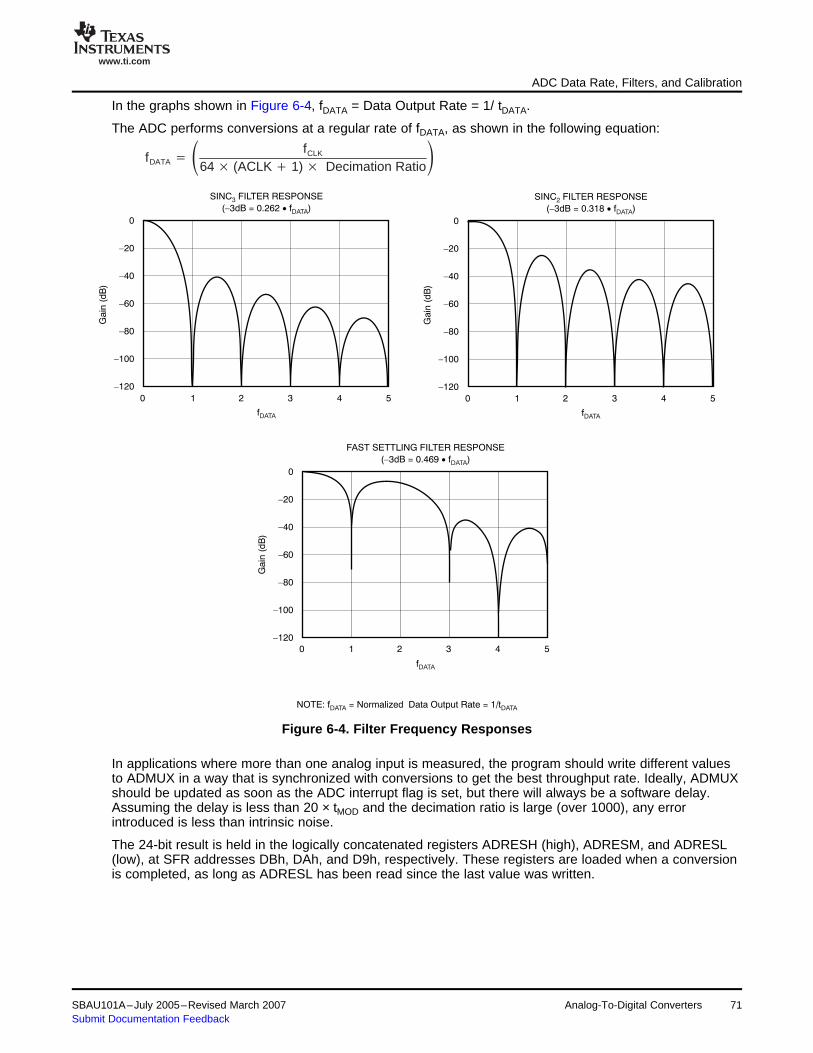
www.ti.com
fDATA fCLK
64 (ACLK 1) Decimation Ratio
SINC FILTER RESPONSE3
( 3dB = 0.262 f- · )DATA
fDATA
0
-20
-40
-60
-80
-100
-120
0 1 2 3 4 5 0 1 2 3 4 5
0 1 2 3 4 5
Ga
in (
dB
)
SINC FILTER RESPONSE2
( 3dB = 0.318 f- · )DATA
fDATA
0
-20
-40
-60
-80
-100
-120
Gain
(dB
)
FAST SETTLING FILTER RESPONSE
( 3dB = 0.469 f- · )DATA
fDATA
0
-20
-40
-60
-80
-100
-120
NOTE: f = Normalized Data Output Rate = 1/tDATA DATA
Gain
(dB
)
ADC Data Rate, Filters, and Calibration
In the graphs shown in Figure 6-4, fDATA = Data Output Rate = 1/ tDATA.
The ADC performs conversions at a regular rate of fDATA, as shown in the following equation:
Figure 6-4. Filter Frequency Responses
In applications where more than one analog input is measured, the program should write different valuesto ADMUX in a way that is synchronized with conversions to get the best throughput rate. Ideally, ADMUXshould be updated as soon as the ADC interrupt flag is set, but there will always be a software delay.Assuming the delay is less than 20 × tMOD and the decimation ratio is large (over 1000), any errorintroduced is less than intrinsic noise.
The 24-bit result is held in the logically concatenated registers ADRESH (high), ADRESM, and ADRESL(low), at SFR addresses DBh, DAh, and D9h, respectively. These registers are loaded when a conversionis completed, as long as ADRESL has been read since the last value was written.
SBAU101A–July 2005–Revised March 2007 Analog-To-Digital Converters 71Submit Documentation Feedback

www.ti.com
6.7 32-Bit Summation Register
32-Bit Summation Register
In devices that have the AIPOL register (MSC1211/12/13/14), reading AIE may return the mask bits thatwere previously written. Therefore, these devices support read/modify/write instructions such as ORLAIE,#020H to enable the ADC interrupt and ANL AIE,#0BFH to disable the summation interrupt. However,this code must not be used with other devices where reading AIE returns the value of the interrupt flagsbefore masking. To allow dynamic modification of interrupt enable bits on these parts, the programmershould first manipulate a byte in memory with read/modify/write instructions, and then copy it to AIE. If thememory byte is updated by a sequence of instructions, in general the codee should be protected frominterrupts.
Table 6-6. ADC Interrupt ControlsBit 5 of AIE at A6h Bit 5 of AISTAT at A7h Bit 5 of AIPOL at A4h
Family Part Enable ADC Interrupt ADC Interrupt Status Flag ADC Interrupt Poll
Write: Read: Read:
0: Masked 0: Inactive or masked ADC interrupt flag beforemasking (RDSEL = 1) or value ofMSC1211 1: Enabled 1: Active EADC (RDSEL = 0).MSC1212
MSC1213 Read: While active, no new data will be written toMSC1214 ADRES. Cleared by reading ADRESL at
ADC interrupt flag before D9h.masking (RDSEL = 0) or value ofEADC (RDSEL = 1).
Write: Read:
0: Masked 0: Inactive or masked
1: Enabled 1: ActiveMSC1210 Not Present
Read: While active, no new data will be written toADRES. Cleared by reading ADRESL at
Mask Value D9h.
When the MSC121x is reset, default values are loaded into the digital offset and digital gain calibrationregisters associated with the ADC; specifically, for offset OCH:OCM:OCL = 00000000h and for gainGCH:GCM:GCL = 5FEC5Ah. (See Application Note SBAA099, Calibration Routines and Register ValueGeneration for the ADS121x Series, for additional information.) Although the ADC will then produce anoutput that varies linearly with the differential input voltage, it will not have the correct scale. A program isable to write any desired value to these calibration SFRs, but is most likely to set the CAL bits in ADCON0to force an internal calibration for offset and gain (CAL = 001). A differential input of VREF = (REF IN+) –(REF IN–) will then map to a full-scale digital output. Alternatively, the overall system can be placed into adefined zero state and then calibrated for offset (CAL = 100) followed by a full-scale condition andcalibrated for gain (CAL = 101). Each type of calibration takes seven tDATA periods, as summarized inTable 6-5 . For instance, CAL = 001 takes 14 tDATA periods. For best results, calibration should beperformed with the Sinc3 or Auto filter selected.
To use the 32-bit summation register, either under the control of the CPU and/or the ADC, bit 3 of PDCONat F1h must be '0'. Operations are controlled by SSCON at E1h, with data accessed via SUMR3:SUMR0.
Table 6-7. Summation RegisterRegister Address Read Write
Name (Hex) Summation Register Temporary Regiter
SUMR3 E5 Bits 31 to 24 (most significant) Bits 31 to 24 (most significant)
SUMR2 E4 Bits 23 to 16 Bits 23 to 16
SUMR1 E3 Bits 15 to 8 Bits 15 to 8
SUMR0 E2 Bits 7 to 0 (least significant) Bits 7 to 0 (least significant)
72 Analog-To-Digital Converters SBAU101A–July 2005–Revised March 2007Submit Documentation Feedback
www.ti.com
32-Bit Summation Register
Table 6-8. SSCON—Summation/Shift ControlSSCON SFR E1h Reset Value = 00h
Bit Name and Number
S S S S SS S S S S S S S Action or InterpretationC C C C C S S S where:O O N N N H H H Read of Summation Register = AN N T T T F F F Write to Temporary Register = B1 0 2 1 0 2 1 0
7 6 5 4 3 2 1 0
0 0 x x x x x x Select CPU summation mode for MSC12x
0 0 0 0 0 0 0 0 Clear Summation register, A = zero (1)
0 0 0 1 0 0 0 0 Change to summation mode (2) (3)
Next CPU summation on write to SUMR0, A = A + B
0 0 1 0 0 0 0 0 Change to subtraction mode (2) (3)
Next CPU subtraction on write to SUMR0, A = A - B
1 0 0 0 0 S S S Shift right by (SSSb + 1) bits
0 1 C C C 0 0 0 Add ADC conversions to Summation register 2(CCC+1) times (that is, 2 to 256 times).
1 1 C C C S S S Add ADC conversions to Summation register 2(CCC+1) times (that is, 2 to 256 times). Thenshift right by (SSSb + 1) bits and set the summation complete interrupt flag.
(1) For the MSC1210, writing 00h to SSCON clears the 32-bit hardware accumulator and selects CPU controlled summation. Forother devices, the 32-bit hardware accumulator is cleared, but the mode is not changed.
(2) These operations are not available in the MSC1210.(3) If the polarity bit in ADCON1 at DDh is 0, the 24-bit ADC conversion is sign-extended to 32 bits. That is, bit 7 of ADRESH is
propagated to all higher bits.
Immediately after a CPU instruction writes data to SUMR0, it may trigger an addition, subtraction, or shiftoperation, depending on the value of SSCON. Addition and subtraction take a single cycle, tCLK. Shifting isperformed either 1 or 2 bits per cycle, and takes up to four tCLK periods to complete.
Table 6-9. Summation Interrupt ControlsBit 6 of AIE at A6h Bit 6 of AISTAT at A7h Bit 6 of AIPOL at A4h
Family Part Enable Summation Interrupt Summation Interrupt Status Flag Summation Interrupt Poll
Write: Read: Read:
0: Masked 0: Inactive or masked Summation interrupt flag beforemasking (RDSEL = 1) or value ofMSC1211 1: Enabled 1: Active ESUM (RDSEL = 0).MSC1212
MSC1213 Read: While active, no new data will be written toMSC1214 SUMR. Cleared by reading SUMR0 at
Summation interrupt flag before E2h.masking (RDSEL = 0) or value ofESUM (RDSEL = 1).
Write: Read:
0: Masked 0: Inactive or masked
1: Enabled 1: ActiveMSC1210 Not Present
Read: While active, no new data will be written toSUMR. Cleared by reading SUMR0 at
Mask Value E2h.
SBAU101A–July 2005–Revised March 2007 Analog-To-Digital Converters 73Submit Documentation Feedback

www.ti.com
6.8 Accessing the ADC Multi-Byte Conversion in C
Accessing the ADC Multi-Byte Conversion in C
ADRESH:ADRESM:ADRESL represent a 24-bit register, while SUMR3:SUMR2:SUMR1:SUMR0 representa 32-bit register. It is often useful to map both of these to long integers in C, but care should be taken. Forexample, assuming that the variable sum has been declared to be of type "signed long int," it is temptingto write:sum = SUMR3 << 24 + SUMR2 << 16 + SUMR1 << 8 + SUMR0;
However, this produces a pattern-dependent incorrect value because of the (ANSI-defined) 16-bit integerpromotion rules within most compilers for the 8051 family.
Changing to:sum = ((unsigned long)SUMR3 << 24) + ((unsigned long)SUMR2 << 16)
+ ((unsigned long)SUMR1 << 8) + (unsigned long)SUMR0;
will produce the expected value, but may take between approximately 800 and 1200 machine cycles, ascompilers call run-time libraries to achieve multi-bit shifts. Since the order of additions is not defined in C,it is possible that SUMR0 is accessed first and the ADC interrupt flag is cleared. If other interrupts arepresent and their service routines take more time to complete than the next conversion, SUMR3, 2, 1 maybe overwritten before being used to complete the evaluation of the expression.
Another approach is to define a union to overlay byte-wide variables with a 4-byte long integer.typedef union
unsigned long v;char va[4];struct char v3,v2,v1,v0; vs; type_sumv;
type_sumv data s; //variable s is placed in `core' on-chip data space
Then use:s.vs.v3=SUMR3;s.vs.v2=SUMR2;s.vs.v1=SUMR1;s.vs.v0=SUMR0; // SUMR0 is accessed lastreading = f(s.v); // some function of the 4-byte variable v.s
Alternatively, array elements may be used, but the order of subscripts is reversed.s.va[0]=SUMR3;s.va[1]=SUMR2;s.va[2]=SUMR1;s.va[3]=SUMR0;
Although the code needed to access the union may appear clumsy, it maps to simple inlineassembly-level MOV instructions that take 3 × 4 = 12 machine cycles to execute. In other words, it isapproximately 100 times faster than using multiple shifts.
In the next example, the ADC results register is read using an assembly-level program, which makesexpressions in C more intuitive. This technique may also be used to read the summation register.
74 Analog-To-Digital Converters SBAU101A–July 2005–Revised March 2007Submit Documentation Feedback

www.ti.com
6.9 ADC Example Program
ADC Example Program
Example 6-1 shows how the ADC may be used in a polled environment with a foreground activity thatproduces a pseudo-random binary data stream. The number of characters output per line equals thetemperature of the MSC121x in degrees Celsius (°C). The main program is written in C and calls the bootROM to determine the baud rate and an assembly language function to read the ADC conversion. It isintended for use directly with Texas Instruments' MSC1210-DAQ-EVM or full EVMs with an appropriatevalue for ACLK.
Example 6-1. ADC Program
// Polledadc.c - Pseudo Random Binary Sequence generator with Polled ADC// MSC1210 EVM Switches 1:On SW3-12345678 SW6-12345678// 0:Off 11110111 11110000#include <Reg1210.h>#include <stdio.h>sbit RedLed = P3^4; // RED LED on EVMsbit YellowLed = P3^5; // Yellow LED on EVMcode at 0xFFF3 void autobaud(void);extern signed long bipolar(void); // reads ADC valuevoid main(void) data char mask=0x8E, r=1,n,j,x, temp=50, count=255;data signed long reading; data int iy; data float y;
//PDCON = 0x0f7; // would turn adc on, but turn other subsystems off//PDCON &=~0b00001000; // turns on adc and leaves other subsystems unchangedPDCON &=~0x08; // turns on adc and leaves other subsystems unchanged//ACLK = 2; // ACLK frequency = 1.8432MHz/(2+1) = 0.6144MHz for MSC1210-DAQEVMACLK = 17; // = 11.0592MHz/(17+1) = 0.6144MHz for MSC1210EVM
//ACLK = 35; // = 22.1184MHz/(35+1) = 0.6144MHz for MSC1211EVMDECIMATION = 1920 ; // => 200ms per conversion
//ODAC=0; // offset DAC is zero after RESET//ADCON0 = 0b00100000; // BOD off, Vref on, 1.25V, Buff off, PGA 1ADCON0 = 0x20; // BOD off, Vref on, 1.25V, Buff off, PGA 1autobaud();printf("MSC121x Random bit generator with polled ADC\n");printf("Readings begin in (14+3)*200ms = 3.4 seconds \n");ADMUX = 0xff; // Select Temperature diodesADCON1 = 0x01; // bipolar, auto mode, self calibration - offset and gainfor (j=0;j<3;j++) while (!(AIE & 0x020)) reading=bipolar(); // discard 3 conversions after calibration
RI_0 = 0; // Clear received flag in USARTwhile (!(AIE & 0x20)); // wait for conversionwhile(1)while(!RI_0)
if (AIE & 0x20) // test ADC interrupt flagreading=bipolar(); // get reading and clear flag
// y=(reading-692199)/2534.1; // simple theoretical// y=(reading-700875)/2567.1; // convert to Degrees C (empirical 1)
y=(reading-704509)/2595.1; // convert to Degrees C (empirical 2)iy=y+0.5; // nearest integerif ((iy>0) && (iy<50)) temp=iy; // clamp range
if (count>=temp) // if line length >= temperatureprintf("\n%3d ",temp); // output new line and temperatureYellowLed=RedLed;
count=0;
SBAU101A–July 2005–Revised March 2007 Analog-To-Digital Converters 75Submit Documentation Feedback

www.ti.com
ADC Example Program
Example 6-1. ADC Program (continued)
n=r & mask; // PRBS generator with 4-bit feedbackj=0; // j will become the sum of 1's in nwhile (n)
n&=(n-1); j++;r=(r+r)+(j&1); // shift r left with LSB of sumif (r&1) putchar('*'); // Note: putchar takes 28 machine cycleselse printf("."); // but printf takes 354 machine cyclescount++; // increment character count
RI_0 = 0;while(!RI_0); // wait for characterRI_0 = 0; // continue
From TI fileUtilities.A51:File name: utilities.a51;; Copyright 2003 Texas Instruments Inc as an unpublished work.; All Rights Reserved.;; Revision History; Version 1.1;; Assembler Version (Keil V2.38), (Raisonance V6.10.13);; Module Description:; ADC routines to read 24-bit ADC and return the value as a long integer.
;*********************************************************************$include (legal.a51) ; Texas Instruments, Inc. copyright and liability$include (reg1210.inc);*********************************************************************PUBLIC unipolar, bipolar, read_sum_regsadc_sub SEGMENT CODE
RSEG adc_sub
;;;;;;;;;;;;;;;;;;;;;; unsigned long unipolar(void); return the 3 byte adres to R4567 (MSB~LSB); unsigned long int with R4=0unipolar:
mov r4,#0mov r5,adreshmov r6,adresmmov r7,adreslret
;;;;;;;;;;;;;;;;;;;;;; signed long bipolar(void); return the 3 byte adres to R4567 (MSB~LSB); return signed long int with sign extendsion on R4bipolar:
mov r4,#0mov a,adreshmov r5,amov r6,adresmmov r7,adresljnb acc.7,positivemov r4,#0ffh
positive:ret
76 Analog-To-Digital Converters SBAU101A–July 2005–Revised March 2007Submit Documentation Feedback

www.ti.com
ADC Example Program
Example 6-1. ADC Program (continued)
;;;;;;;;;;;;;;;;;;;;;; signed long read_sum_regs(void); return the 4 byte sumr to R4567 (MSB~LSB); return signed long int, sign extension done by hardwareread_sum_regs:
mov r4, SUMR3;mov r5, SUMR2;mov r6, SUMR1;mov r7, SUMR0;ret
end
Produces:MSC121x Random bit generator with polled ADCReadings begin in (14+3)*200ms = 3.4 seconds25 .**...****.*....********.25 .*....*.*..*****.*.*.*.**25 *.....**...*.*.**..**..*.25 ******.****..**.***.***..*26 .*.*..*.*...*..*.**.*...**26 ..***..****...**.**....*...27 *.***.*.****.**.*****....**27 .*..**.*.**.**.*.*.....*..*27 **.**..*..*..**......***.*..28 *...***...*.......*.**...***28 *.*....********..*....*.*..*28 ****.*.*.*.***.....**...*.*.28 **..**..*.******.****..**.**28 *.***..*.*.*..*.*...*..*.**.28 *...**..***..****...**.**....29 *...*.***.*.****.**.*****....29 **.*..**.*.**.**.*.*.....*..*
Note: The temperature is shown in degrees Celsius (°C) followed by the same number ofpseudo-random characters. The temperature was increased from 25°C to 29°C bytouching the MSC121x with a finger.
The .**...****. pattern repeates every 255 characters.
SBAU101A–July 2005–Revised March 2007 Analog-To-Digital Converters 77Submit Documentation Feedback

www.ti.com
Analog-To-Digital Converters78 SBAU101A–July 2005–Revised March 2007Submit Documentation Feedback

Chapter 7SBAU101A–July 2005–Revised March 2007
Digital-To-Analog Converters
This chapter describes the digital-to-analog converters (DACs) of the MSC121x.
Topic ........................................................................................................... Page
7.1 Introduction....................................................................................... 807.2 DAC Selection ................................................................................... 817.3 DAC Configuration and Control ........................................................... 837.4 DAC Technology and Limitations......................................................... 847.5 DAC Example Program ....................................................................... 84
SBAU101A–July 2005–Revised March 2007 Digital-To-Analog Converters 79Submit Documentation Feedback
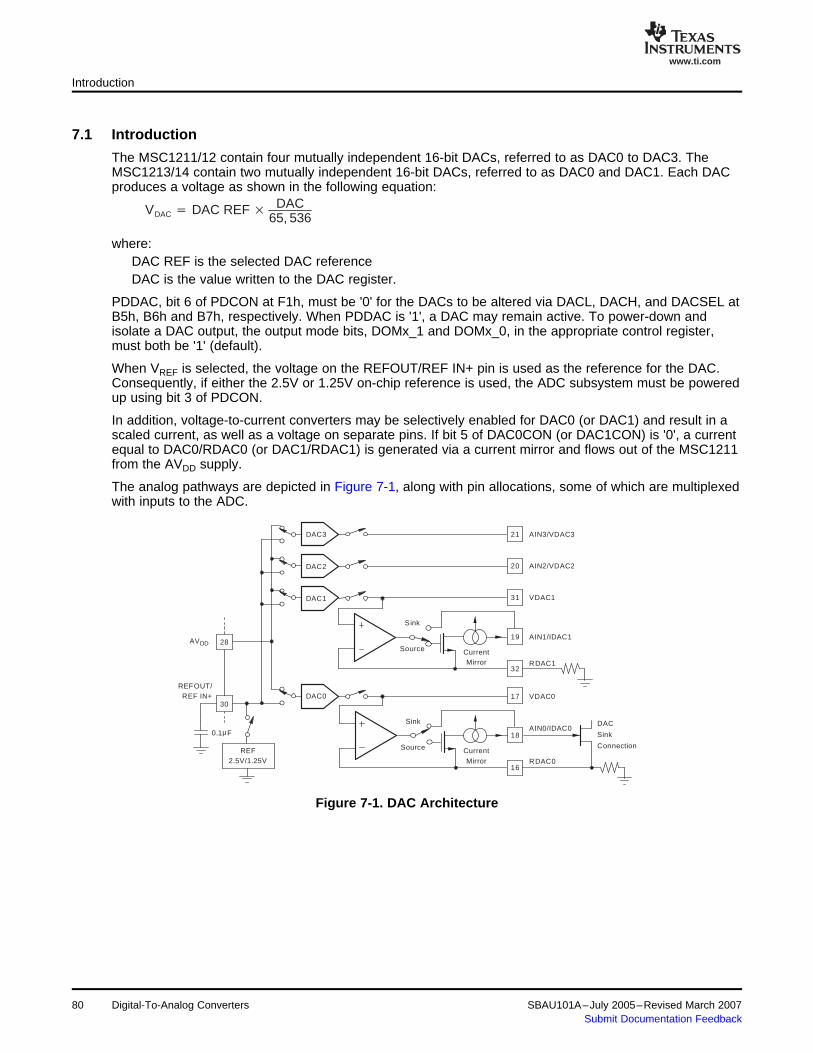
www.ti.com
7.1 Introduction
VDAC DAC REF DAC65, 536
DAC3
DAC2
DAC1
DAC0
21 AIN3/VDAC3
AIN2/VDAC2
VDAC1
VDAC0
DAC
Sink
Connection
AIN0/IDAC0
RDAC0
AIN1/IDAC1
RDAC1
20
31
19
32
17
CurrentMirror
CurrentMirror
18
16
Sink
Source
Sink
Source
REFOUT/REF IN+
AVDD
30
REF2.5V/1.25V
28
0.1µF
Introduction
The MSC1211/12 contain four mutually independent 16-bit DACs, referred to as DAC0 to DAC3. TheMSC1213/14 contain two mutually independent 16-bit DACs, referred to as DAC0 and DAC1. Each DACproduces a voltage as shown in the following equation:
where:DAC REF is the selected DAC referenceDAC is the value written to the DAC register.
PDDAC, bit 6 of PDCON at F1h, must be '0' for the DACs to be altered via DACL, DACH, and DACSEL atB5h, B6h and B7h, respectively. When PDDAC is '1', a DAC may remain active. To power-down andisolate a DAC output, the output mode bits, DOMx_1 and DOMx_0, in the appropriate control register,must both be '1' (default).
When VREF is selected, the voltage on the REFOUT/REF IN+ pin is used as the reference for the DAC.Consequently, if either the 2.5V or 1.25V on-chip reference is used, the ADC subsystem must be poweredup using bit 3 of PDCON.
In addition, voltage-to-current converters may be selectively enabled for DAC0 (or DAC1) and result in ascaled current, as well as a voltage on separate pins. If bit 5 of DAC0CON (or DAC1CON) is '0', a currentequal to DAC0/RDAC0 (or DAC1/RDAC1) is generated via a current mirror and flows out of the MSC1211from the AVDD supply.
The analog pathways are depicted in Figure 7-1, along with pin allocations, some of which are multiplexedwith inputs to the ADC.
Figure 7-1. DAC Architecture
80 Digital-To-Analog Converters SBAU101A–July 2005–Revised March 2007Submit Documentation Feedback

www.ti.com
7.2 DAC Selection
DAC Selection
Each DAC has an 8-bit control register, a buffered 16-bit data register, and two additional bits, whichdetermine the way that the output data register is loaded.
Three SFRs are used to access and control the DACs using an indirect addressing scheme. Thisconfiguration makes accessing each DAC more involved than simply writing to independent SFRs, but hasthe advantage of using the SFR memory space efficiently.
The DAC select register (SFR B7h), determines the individual DAC buffer or control register to beaccessed, as well as the shared Load Control Register. The interpretation of SFRs B6h and B5h dependsupon the value in DACSEL, as shown in Table 7-1.
Table 7-1. DACSEL ValuesDACSEL (B7h) DACH (B6h) DACL (B5h) Reset Value
00h DAC0 (high) DAC0 (low) 0000h
01h DAC1 (high) DAC1 (low) 0000h
02h DAC2 (high) DAC2 (low) 0000h
03h DAC3 (high) DAC3 (low) 0000h
04h DAC1CON DAC0CON 6363h
05h DAC3CON DAC2CON 0303h
06h — LOADCON xx00h
07h to FFh Reserved Reserved Reserved
The way a DAC output register is loaded is determined by two bits in the Load Control Register(LOADCON) as shown in Table 7-2 and Table 7-3. The LOADCON register is accessed indirectly via theSFR at B5h when DACSEL = 06h.
Table 7-2. LOADCON SFRDACSEL = 7 6 5 4 3 2 1 0 Reset Value06h
DAC3 DAC2 DAC1 DAC0SFR B5h 00h
D3LOAD1 D3LOAD0 D2LOAD1 D2LOAD0 D1LOAD1 D1LOAD0 D0LOAD1 D0LOAD0
Table 7-3. DxLOAD Output Modes for DACxDxLOAD[1:0] DxLOAD Output Mode for DACx
A write to the DAC high byte (DACxH) is directed to the upper byte of the 16-bit data buffer and does not alterDirect Load the output register.
00 A write to the DAC low byte (DACxL) is directed to the lower byte of the 16-bit data buffer, which is immediatelycopied to the output register.
Delayed load Values are written to the DACxH/DACxL16-bit data buffer, which will be transferred to the DAC output register01 on the next tick of the MSEC system timer register (see SFRs FDh and FCh).
Delayed load Values are written to the DACxH/DACxL16-bit data buffer, which will be transferred to the DAC output register10 on the next tick of the HMSEC system timer register (see SFR FEh)
Synchronized load Values are written to the DACxH/DACxL16-bit data buffer, which will be transferred to the DAC output register11 when 11b is (re)written to these bits.
SBAU101A–July 2005–Revised March 2007 Digital-To-Analog Converters 81Submit Documentation Feedback
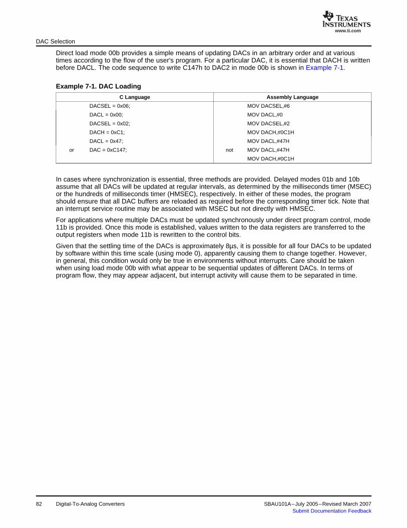
www.ti.com
DAC Selection
Direct load mode 00b provides a simple means of updating DACs in an arbitrary order and at varioustimes according to the flow of the user's program. For a particular DAC, it is essential that DACH is writtenbefore DACL. The code sequence to write C147h to DAC2 in mode 00b is shown in Example 7-1.
Example 7-1. DAC Loading
C Language Assembly Language
DACSEL = 0x06; MOV DACSEL,#6
DACL = 0x00; MOV DACL,#0
DACSEL = 0x02; MOV DACSEL,#2
DACH = 0xC1; MOV DACH,#0C1H
DACL = 0x47; MOV DACL,#47H
or DAC = 0xC147; not MOV DACL,#47H
MOV DACH,#0C1H
In cases where synchronization is essential, three methods are provided. Delayed modes 01b and 10bassume that all DACs will be updated at regular intervals, as determined by the milliseconds timer (MSEC)or the hundreds of milliseconds timer (HMSEC), respectively. In either of these modes, the programshould ensure that all DAC buffers are reloaded as required before the corresponding timer tick. Note thatan interrupt service routine may be associated with MSEC but not directly with HMSEC.
For applications where multiple DACs must be updated synchronously under direct program control, mode11b is provided. Once this mode is established, values written to the data registers are transferred to theoutput registers when mode 11b is rewritten to the control bits.
Given that the settling time of the DACs is approximately 8µs, it is possible for all four DACs to be updatedby software within this time scale (using mode 0), apparently causing them to change together. However,in general, this condition would only be true in environments without interrupts. Care should be takenwhen using load mode 00b with what appear to be sequential updates of different DACs. In terms ofprogram flow, they may appear adjacent, but interrupt activity will cause them to be separated in time.
Digital-To-Analog Converters82 SBAU101A–July 2005–Revised March 2007Submit Documentation Feedback
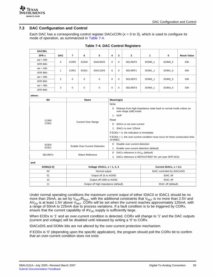
www.ti.com
7.3 DAC Configuration and Control
DAC Configuration and Control
Each DAC has a corresponding control register DACxCON (x = 0 to 3), which is used to configure itsmode of operation, as summarized in Table 7-4.
Table 7-4. DAC Control RegistersDACSEL
SFR x DAC 7 6 5 4 3 2 1 0 Reset Value
sel = 04h0 COR0 EOD0 IDAC0DIS 0 0 SELREF0 DOM0_1 DOM0_0 63h
SFR B5h
sel = 04h1 COR1 EOD1 IDAC1DIS 0 0 SELREF1 DOM1_1 DOM1_0 63h
SFR B6h
sel = 05h2 0 0 0 0 0 SELREF2 DOM3_1 DOM2_0 03h
SFR B5h
sel = 05h3 0 0 0 0 0 SELREF3 DOM3_1 DOM3_0 03h
SFR B6h
where:
Bit Name Meaning(s)
Write:
0: Release from high-impedance state back to normal mode unless anover-range (still) exists.
1: NOP
Read:COR0 Current Over RangeCOR1 0: IDACx is not over-current
1: IDACx is over 125mA
If EODx = 0, the indication is immediate.
If EODx = 1, the over-current condition must occur for three consecutive ticksof MSEC.
0: Disable over-current detectionEOD0 Enable Over-Current DetectionEOD1 1: Enable over-current detection (default)
0: DACx reference is AVDD (default)SELREFx Select Reference
1: DACx reference is REFOUT/REF IN+ pin (see SFR DCh)
and:
DOMx[1:0] Voltage VDACx, x = 1, 2, 3 Current IDACx, x = 0,1
00 Normal output IDAC controlled by IDACxDIS
01 Output off 1k to AGND IDAC off
10 Output off 100k to AGND IDAC off
11 Output off high impedance (default) IDAC off (default)
Under normal operating conditions the maximum current output of either IDAC0 or IDAC1 should be nomore than 25mA, as set by VREF/RREF, with the additional constraints that VREF is no more than 2.5V andAVDD is at least 1.5V above VREF. CORx will be set when the current reaches approximately 125mA, witha range of 50mA to 225mA due to process variations. If a fault condition is to be triggered by CORx,ensure that the current capability of AVDD supply is sufficiently large.
When EODx is '1' and an over-current condition is detected, CORx will change to '1' and the DAC outputs(current and voltage) will be disabled until released by writing a '0' to CORx.
IDACxDIS and DOMx bits are not altered by the over-current protection mechanism.
If EODx is '0' (depending upon the specific application), the program should poll the CORx bit to confirmthat an over-current condition does not exist.
SBAU101A–July 2005–Revised March 2007 Digital-To-Analog Converters 83Submit Documentation Feedback
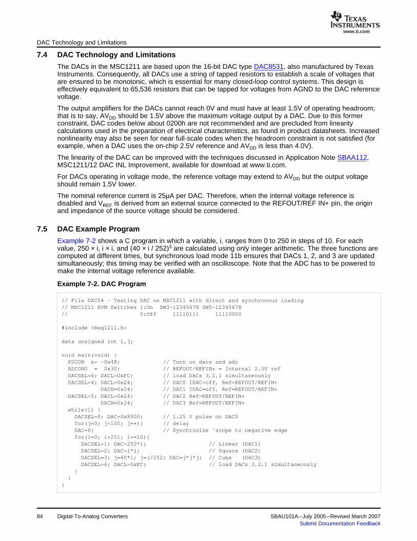
www.ti.com
7.4 DAC Technology and Limitations
7.5 DAC Example Program
DAC Technology and Limitations
The DACs in the MSC1211 are based upon the 16-bit DAC type DAC8531, also manufactured by TexasInstruments. Consequently, all DACs use a string of tapped resistors to establish a scale of voltages thatare ensured to be monotonic, which is essential for many closed-loop control systems. This design iseffectively equivalent to 65,536 resistors that can be tapped for voltages from AGND to the DAC referencevoltage.
The output amplifiers for the DACs cannot reach 0V and must have at least 1.5V of operating headroom;that is to say, AVDD should be 1.5V above the maximum voltage output by a DAC. Due to this formerconstraint, DAC codes below about 0200h are not recommended and are precluded from linearitycalculations used in the preparation of electrical characteristics, as found in product datasheets. Increasednonlinearity may also be seen for near full-scale codes when the headroom constraint is not satisfied (forexample, when a DAC uses the on-chip 2.5V reference and AVDD is less than 4.0V).
The linearity of the DAC can be improved with the techniques discussed in Application Note SBAA112,MSC1211/12 DAC INL Improvement, available for download at www.ti.com.
For DACs operating in voltage mode, the reference voltage may extend to AVDD but the output voltageshould remain 1.5V lower.
The nominal reference current is 25µA per DAC. Therefore, when the internal voltage reference isdisabled and VREF is derived from an external source connected to the REFOUT/REF IN+ pin, the originand impedance of the source voltage should be considered.
Example 7-2 shows a C program in which a variable, i, ranges from 0 to 250 in steps of 10. For eachvalue, 250 × i, i × i, and (40 × i / 252)3 are calculated using only integer arithmetic. The three functions arecomputed at different times, but synchronous load mode 11b ensures that DACs 1, 2, and 3 are updatedsimultaneously; this timing may be verified with an oscilloscope. Note that the ADC has to be powered tomake the internal voltage reference available.
Example 7-2. DAC Program
// File DAC04 - Testing DAC on MSC1211 with direct and synchronous loading// MSC1211 EVM Switches 1:On SW3-12345678 SW5-12345678// 0:Off 11110111 11110000
#include <Reg1211.h>
data unsigned int i,j;
void main(void) PDCON &= ~0x48; // Turn on dacs and adcADCON0 = 0x30; // REFOUT/REFIN+ = Internal 2.5V refDACSEL=6; DACL=0xFC; // load DACs 3,2,1 simultaneouslyDACSEL=4; DACL=0x24; // DAC0 IDAC=off, Ref=REFOUT/REFIN+
DACH=0x24; // DAC1 IDAC=off, Ref=REFOUT/REFIN+DACSEL=5; DACL=0x24; // DAC2 Ref=REFOUT/REFIN+
DACH=0x24; // DAC3 Ref=REFOUT/REFIN+while(1) DACSEL=0; DAC=0x8000; // 1.25 V pulse on DAC0for(j=0; j<100; j++); // delayDAC=0; // Synchronize 'scope to negative edgefor(i=0; i<251; i+=10)
DACSEL=1; DAC=250*i; // Linear (DAC1)DACSEL=2; DAC=i*i; // Square (DAC2)DACSEL=3; j=40*i; j=j/252; DAC=j*j*j; // Cube (DAC3)DACSEL=6; DACL=0xFC; // load DACs 3,2,1 simultaneously
84 Digital-To-Analog Converters SBAU101A–July 2005–Revised March 2007Submit Documentation Feedback

Chapter 8SBAU101A–July 2005–Revised March 2007
Pulse-Width Modulator and Tone Generator
This chapter describes the pulse-width modulator (PWM) and tone generator of the MSC121x.
Topic ........................................................................................................... Page
8.1 Description........................................................................................ 868.2 PWM Generator Example .................................................................... 87
SBAU101A–July 2005–Revised March 2007 Pulse-Width Modulator and Tone Generator 85Submit Documentation Feedback

www.ti.com
8.1 Description
Description
The PWM subsystem consists of the following components:
• 6-bit control register PWMCON• 16-bit Period register (P) and 16-bit Duty register (D), which share the same SFR addresses• 16-bit down-counter, 16-bit comparator, and a finite state machine• A single output pin shared with bit 3 of Port 3
The PWM subsystem is enabled by:
1. Making bit 4 of PDCON at F1h equal to 02. Making bit 3 of P3 equal to 13. Configuring bit 3 of Port 3 to be a standard 8051 port, or open drain. This configuration is achieved by
writing '002' or '102' to bits 7 and 6, respectively, of P3DDRL.
The mode of operation is determined by bits within PWMCON, as summarized in Table 8-1.
Table 8-1. PWMCON—PWM Control (1)
PWMCON SFR A1h Reset Value = 00h
Bit # Name Action or Interpretation
7 — Not used
6 — Not used
Period Polarity
5 PPOL 0: Duty register determines the time the PWM output is high
1: Duty register determines the time the PWM output is low
PWM Register Select
4 PWMSEL 0: Data written to PWLHI:PWMLO, at A3h and A2h, respectively, will be directed to the Period register
1: Data written to PWLHI:PWMLO, at A3h and A2h, respectively, will be directed to the Duty register
Speed Select
3 SPDSEL If 1, the down counter is clocked every tCLK seconds.
Otherwise, the down counter is clocked every tCLK× (USEC+1), where USEC is the 5-bit SFR at FBh.
000: Disable High Impedance = HiZ
001: PWM If PPOL is 0, then output is high for D every P and Duty cycle = D/PIf PPOL is 1, then output is low for D every P and Duty cycle = (P–D)/P2-0 TPCNTL (1)
011: Square Low for P; High for P
111: Staircase High for (P–Z); HiZ for Z; Low for (P–Z); HiZ for Z(1) P = Period[15:0] + 1; D = Duty[15:0]; Z = Period[15:2] (that is, the integer part of Period divided by 4). For large P, Z is
approximately P/4.
The PWM output may be filtered to give a dc level, or used directly in switching systems with inherentfiltering to produce a variable effect. Typical examples of the latter are the brilliance control of a lamp, thepower of a heating element, or the speed control of a dc motor.
When the staircase mode is used, the output repeats as a (strong 1, High-Z, strong 0, and High-Z).
If a PWM signal is used in a closed-loop, real-time control system, the Duty register will be regularlyupdated as part of normal operation. Since this 16-bit register is modified by writing to two 8-bit SFRs,there is a possibility that either an interrupt will occur between the writes, or the PWM generator will usethe Duty register between writes. In either case, one or more cycles may occur with the wrong 16-bit valueand cause undesired perturbation of the controlled system. To avoid this possibility, writes to the Duty (orPeriod, or Tone) register should be protected from interrupts and/or synchronized with changes on pinP3.3. Since this pin is shared, INT1 may be monitored to assist in synchronization in PWM andsquare-wave modes.
In PWM mode, if the value in the Duty register is larger than that in the Period register, the output is heldeither low or high depending on the state of PPOL (bit 5) in PWMCON.
Pulse-Width Modulator and Tone Generator86 SBAU101A–July 2005–Revised March 2007Submit Documentation Feedback

www.ti.com
8.2 PWM Generator Example
PWM Generator Example
Table 8-2. PWM Output
PPOL Condition Duty Cycle % High
0 Period = X, Duty = 0 0
0 0 < Duty ≤ Period Intermediate value
0 Duty > Period 100
1 Period = X, Duty = 0 100
1 0 < Duty ≤ Period Intermediate value
1 Duty > Period 0
Example 8-1 shows how the generator can be configured in PWM, Square, or Staircase modes. It alsoindicates how to use the system timers to produce an interrupt every second. Once a particular mode isselected after reset, it should not be changed until after another reset. However, any mode may bedisabled and then restored.
Example 8-1. PWM Generator
// File TONE4.c - Testing Tone generator// 0:Off 11110111 11110000#include <Reg1211.h>#include <stdio.h>#define xtal 22118400#define divA xtal/440 // Concert pitch 'A'sbit RedLed = P3^4; // RED LED on EVMsbit YellowLed = P3^5; // Yellow LED on EVMdata unsigned char i,tout;typedef enum null, pwm, square, staircase pwmtype;code at 0xFFF3 void autobaud(void);
/* Auxiliary Interrupt */void AuxInt(void) interrupt 6 using 1 char temp;YellowLed=!YellowLed;if (tout) tout--;temp=SECINT; // remove seconds interrupt flagEICON&=~0x10; // remove AI flag
void beep(unsigned int divisor, unsigned char time, pwmtype type) PWMCON&=~0x37; // POL=0, PWMSEL=0, disableTONE=divisor; // Period registerswitch(type) case null: break;case pwm: PWMCON|=0x10; // Duty registerTONE=9*(unsigned long)divisor/10;PWMCON|=1; // pwmbreak;
case square: PWMCON|=3; // squarebreak;
case staircase: PWMCON|=7; // staircasebreak;
tout=time;while(tout);
SBAU101A–July 2005–Revised March 2007 Pulse-Width Modulator and Tone Generator 87Submit Documentation Feedback
www.ti.com
PWM Generator Example
Example 8-1. PWM Generator (continued)
void main(void) PDCON&=~0x12; // power up PWM generator and secondstout=0; // time-out is overMSEC=xtal/1000-1; // 1ms tickHMSEC=100-1; // 100ms tickSECINT=0x89; // write 9 immediately for 10 x 100 msRedLed=0; // indicate start of autobaudautobaud(); // set up serial rateAIE=0x80; // enable Seconds interruptEICON|=0x20; // enable auxiliary interruptPWMCON=0x08; // PWMSEL=Period Register, fclkINT1=1; // Pin P3.3 is highP3DDRL&=~0xC0; // 8051 outputRedLed=1; // indicate waiting for carriage returnwhile(1)printf("\nPress 1 (PWM), 2 (SQUARE) or 3 (STAIRCASE)\n"); // promptRI_0 = 0; // wait for characterwhile(!RI_0);i=SBUF0&3; // limit rangeRI_0=0;printf("Tone in Progress...");switch(i)
case 0 : break;case 1 : beep(divA-1,3,pwm); // parameters computed at compile-timebreak;
case 2 : beep(divA/2-1,4,square); // divA/2-1 is 25133.54, truncated to 0x622dbreak;
case 3 : beep(divA/2-1,5,staircase);
printf("Tone Complete\n");beep(0,1,null);printf("Press Enter or <cr> \n\n");SRST=1; SRST=0; //RESET
88 Pulse-Width Modulator and Tone Generator SBAU101A–July 2005–Revised March 2007Submit Documentation Feedback
Chapter 9SBAU101A–July 2005–Revised March 2007
Inter-IC (I2C) Subsystem
This chapter describes the Inter-IC (I2C) subsystem of the MSC1211 and MSC1213.
Topic ........................................................................................................... Page
9.1 Introduction to the I2C Bus.................................................................. 909.2 I2C Terminology ................................................................................. 909.3 I2C Bus Lines and Basic Timing........................................................... 919.4 I2C Data Transfers and the Acknowledge Bit ......................................... 929.5 I2C Principal Registers........................................................................ 939.6 I2C Related Registers.......................................................................... 969.7 I2C Example—MSC1211/13 as a Master................................................. 979.8 I2C Example—MSC1211/13 as a Slave................................................... 999.9 I2C Example—MSC1211/13 as an Interrupt-Driven Slave........................ 1009.10 I2C Synchronization and Arbitration.................................................... 1019.11 I2C Fast Mode .................................................................................. 1019.12 I2C General Call................................................................................ 1019.13 I2C 10-Bit Addressing........................................................................ 102
SBAU101A–July 2005–Revised March 2007 89Inter-IC (I2C™) SubsystemSubmit Documentation Feedback
www.ti.com
9.1 Introduction to the I2C Bus
9.2 I2C Terminology
Introduction to the I2C Bus
The MSC1211/13 provide hardware support for serial transfers according to the I2C protocol. This protocolwas defined to permit multiple 8-bit transfers between multiple integrated circuits on the same 2-wire bus.At any one time, a bus master coordinates transfers from one slave or to multiple slaves.
For a detailed description of the I2C bus, refer to the I2C-bus specification by Philips.
For many systems where the MSC1211/13 is the only microcontroller, it will be the master, and coordinatethe transfer of data between itself and slave ICs. If active, it can transmit data onto the I2C bus or receivedata from the bus. In either case, it generates the synchronizing clock.
Similarly, where the MSC1211/13 is considered a slave to another microcontroller, it is able to transmitand receive data synchronized by this master.
Many MSC1211/13s can share a single I2C bus where each acts as a master at different times. The activemaster can be determined by software or result from bus arbitration in the event of asynchronouscontention.
Table 9-1 describes selected I2C terms.
Table 9-1. I2C Terminology
Name Description
Transmitter The IC that sends data to the bus
Receiver The IC that receives data from the bus
Master The IC that initiates a transfer, generates clock signals, and terminates a transfer
Slave The IC addressed by a master
Multi-master More than one master can attempt to control the bus at the same time without corrupting the message
Procedure to ensure that if more than one master simultaneously tries to control the bus, only oneArbitration master is allowed to do so and the message is not corrupted
Synchronization Procedure to synchronize the clock signals of two or more ICs
90 SBAU101A–July 2005–Revised March 2007Inter-IC (I2C™) SubsystemSubmit Documentation Feedback
www.ti.com
9.3 I2C Bus Lines and Basic Timing
SCLIN
SCLN1OUT
DATAN1OUT
DATAIN
SCLK
Device 1 Device 2
SDA (Serial Data Line)
Pull−UpResistors
SCL (Serial Clock Line)
+VDD
RP RP
SCLIN
SCLN2OUT
DATAN2OUT
DATAIN
SCLK
SDA
SCL PS
START Condition STOP Condition
SDA
SCL
Data Line Stable,Data Valid
Changeof DataAllowed
I2C Bus Lines and Basic Timing
The I2C bus uses two bidirectional data lines. One is the data line (SDA), and the other is the clock line(SCL). Each is connected to a positive supply voltage via a pull-up resistor; when the bus is free, bothlines are high.
The output stages of I2C interfaces connected to the bus must have an open drain or open collector toperform the wired-AND function. The original specification for the I2C bus allowed the data transfer rate tobe up to 100kbits/s; however, this has been extended to 400kbits/s in fast mode, which is supported bythe MSC1211/13. In either mode, the maximum rate is determined by the value of the pull-up resistors andthe capacitance to ground.
Figure 9-1. I2C Bus Connection of Standard and Fast Mode Devices
Unique START and STOP conditions are identified when SCL is high and SDA changes. If SDA changesfrom 1 to 0, a START condition is created; if SDA changes from 0 to 1, a STOP condition is created. AllICs connected to the bus, including the MSC1211/13, recognize and respond to START and STOPconditions. For a data-bit transfer, SCL is pulsed high while SDA is stable.
Figure 9-2. START and STOP Conditions
Figure 9-3. I2C-Bus Bit Transfer
SBAU101A–July 2005–Revised March 2007 91Inter-IC (I2C™) SubsystemSubmit Documentation Feedback

www.ti.com
9.4 I2C Data Transfers and the Acknowledge Bit
P
SDA
SCL
STOPCondition
S
STARTCondition
1 2 3− 8 9
ACK
9
ACK
7 81 2
MSB
Slave Address Data to Slave
A6 A0 R/W
Acknowledgementfrom Receiver
Byte Complete Clock Line Held Low By Receiver
Acknowledgementfrom Receiver
S
STARTCondition
97 821
AcknowledgementClock Pulse
TransmitterData Output
ReceiverData Output
MasterSCL
I2C Data Transfers and the Acknowledge Bit
Once a master asserts a START condition, the bus is no longer free. The master then transmits eight bitscomprised of the 7-bit address of the slave followed by a read/write (R/W) bit. In a system with multipleasynchronous masters, there may be a period of bus contention and arbitration before the address of theslave is transmitted.
If the slave is to receive data, the R/W bit must be 0; otherwise, it will prepare to transmit data (since theR/W bit is 1). For some I2C devices, such as memories, it is necessary to first write an internal address tothe slave and then read or write data bytes. In this case, a START condition can be re-asserted.
When a master has generated eight SCL pulses, it places its own SDA output high and generates a ninthclock pulse. If the addressed slave has responded, it will have pulled the SDA line low; this represents anacknowledgement (ACK). However, if the addressed slave leaves the SDA line high, the masterrecognizes that the slave has not acknowledged (NACK) the transfer.
Figure 9-4. I2C-Bus Data Transfer
Once addressed, a multi-byte data transfer can be terminated when a slave generates a NACK ratherthan the usual ACK. In addition, after the acknowledge bit, a slave may pull the SCL line low while itperforms local processing; this action often occurs when the slave is a microcontroller that executes atime-consuming interrupt service routine (ISR). While the SCL line is held low, the master will wait.
Figure 9-5. I2C Acknowledge
If a master issues a slave address with a R/W bit that is 1, it will become a master receiver when the slaveresponds with an ACK. Thereafter, the slave provides data bytes to the master, but releases the SDA lineevery ninth clock pulse and samples the acknowledgement that is provided by the master. Typically, themaster will generate ACKs for as long as it expects more data, and then generate a NACK to inform theslave on the last byte.
92 SBAU101A–July 2005–Revised March 2007Inter-IC (I2C™) SubsystemSubmit Documentation Feedback

www.ti.com
9.5 I2C Principal Registers
I2C Principal Registers
There are four principal special function registers (SFRs) associated with the MSC1211/13 I2C interface.These SFRs are:
• I2CCON at 9Ah—provides primary control• I2CDATA at 9Bh—provides data• I2CGCM at 9Ch—provides additional control• I2CSTAT at 9Dh—provides status
The I2C Control register (I2CCON) is described in Table 9-2.
Table 9-2. I2CCON—I2C Control RegisterI2CCON SFR A9h Reset Value = 00h
Bit # Name Action or Interpretation
Read: Current status of START condition or repeated START condition
Write:
0: No actionSTART7 1: Transmit a START conditionvalid only if MSTR = 1
If the bus is not free, a START condition will be transmitted after a STOP condition has been received. If theSTART bit is set after at least one byte has been transmitted, a repeated START condition is transmitted afterthe current data transfer is completed. If both START and STOP are set while the bus is free, a STARTcondition will be followed by a STOP condition.
Read: Current status of STOP condition
Write:
0: No action6 STOP1: Transmit a STOP condition
If both START and STOP are set during a data transfer, a STOP condition is transmitted followed by aSTART condition.
Defines the type of acknowledgement generated during the acknowledge cycle.
Master or slave receiver write:
0: Not acknowledge (NACK, high level on SDA) is generated
5 ACK 1: Acknowledge (ACK, low level on SDA) is generated
Slave transmitter write:
0: The current byte will be the last byte transmitted because NACK occurs
1: One or more bytes to follow the current transaction because ACK occurs.
4 Reserved. Always write '0'.
Write:
3 FAST 0: Standard Mode (100 kHz)
1: Fast Mode (400 kHz)
Write:
2 MSTR 0: Slave mode
1: Master mode
Write:
0: No effect1 SCLS
1: Remove stretch of SCL low, when in slave mode
Allowed only after I2C master has put SCL low.
50ns glitch filter
Write:0 FILEN
0: Filter disabled
1: Filter of approximately 50ns is enabled
SBAU101A–July 2005–Revised March 2007 93Inter-IC (I2C™) SubsystemSubmit Documentation Feedback
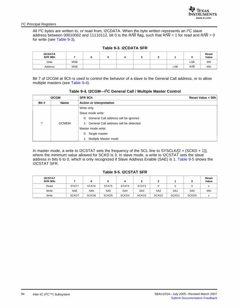
www.ti.com
I2C Principal Registers
All I2C bytes are written to, or read from, I2CDATA. When the byte written represents an I2C slaveaddress between 00010002 and 11110112, bit 0 is the R/W flag, such that R/W = 1 for read and R/W = 0for write (see Table 9-3).
Table 9-3. I2CDATA SFRI2CDATA ResetSFR 9Bh 7 6 5 4 3 2 1 0 Value
Data MSB LSB 00h
Address MSB LSB R/W 00h
Bit 7 of I2CGM at 9Ch is used to control the behavior of a slave to the General Call address, or to allowmultiple masters (see Table 9-4).
Table 9-4. I2CGM—I2C General Call / Multiple Master Control
I2CGM SFR 9Ch Reset Value = 00h
Bit # Name Action or Interpretation
Write only.
Slave mode write:
0: General Call address will be ignored
7 GCMEM 1: General Call address will be detected
Master mode write:
0: Single master
1: Multiple Master mode
In master mode, a write to I2CSTAT sets the frequency of the SCL line to SYSCLK/[2 × (SCKD + 1)],where the minimum value allowed for SCKD is 3. In slave mode, a write to I2CSTAT sets the slaveaddress in bits 6 to 0, which is only recognized if Slave Address Enable (SAE) is 1. Table 9-5 shows theI2CSTAT SFR.
Table 9-5. I2CSTAT SFRI2CSTAT ResetSFR 9Dh 7 6 5 4 3 2 1 0 Value
Read STAT7 STAT6 STAT5 STAT4 STAT3 0 0 0 x
Write SAE SA6 SA5 SA4 SA3 SA2 SA1 SA0 00h
Write SCKD7 SCKD6 SCKD5 SCKD4 SCKD3 SCKD2 SCKD1 SCKD0 x
94 SBAU101A–July 2005–Revised March 2007Inter-IC (I2C™) SubsystemSubmit Documentation Feedback
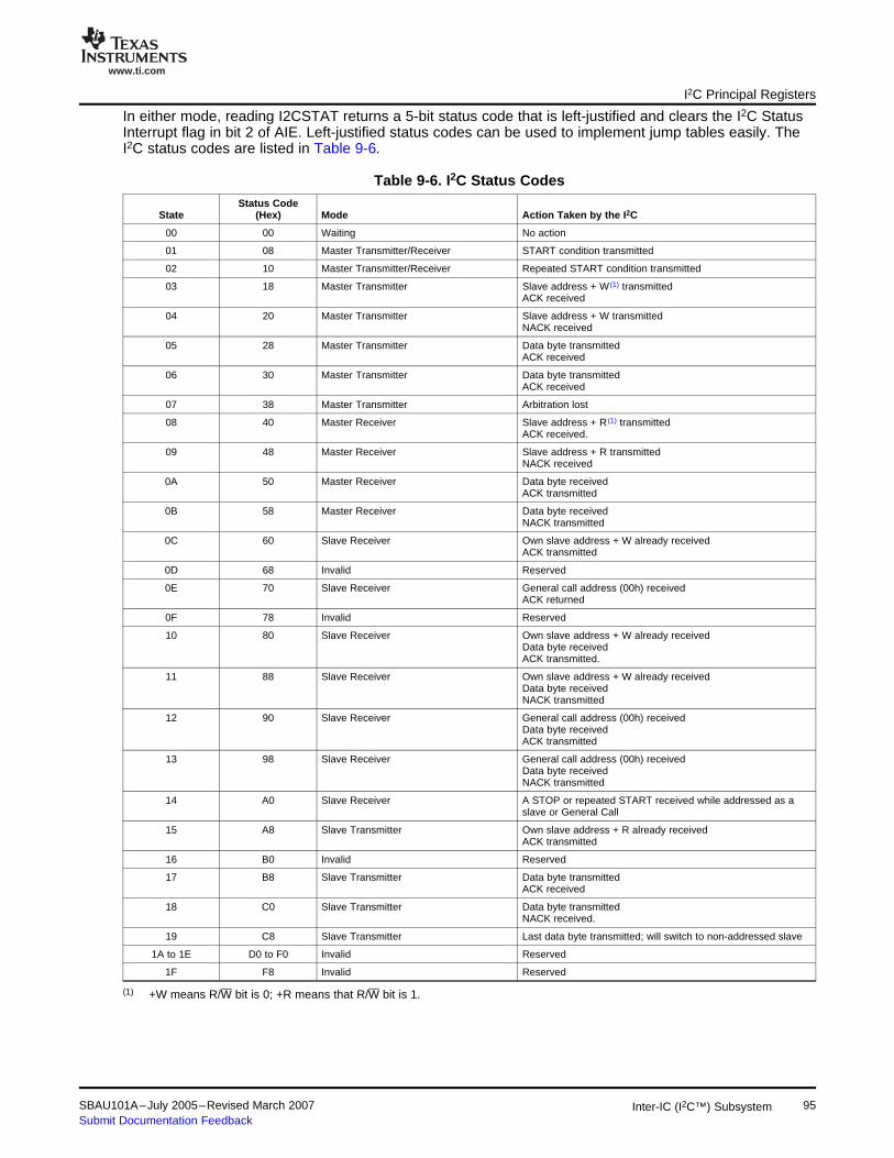
www.ti.com
I2C Principal Registers
In either mode, reading I2CSTAT returns a 5-bit status code that is left-justified and clears the I2C StatusInterrupt flag in bit 2 of AIE. Left-justified status codes can be used to implement jump tables easily. TheI2C status codes are listed in Table 9-6.
Table 9-6. I2C Status CodesStatus Code
State (Hex) Mode Action Taken by the I2C
00 00 Waiting No action
01 08 Master Transmitter/Receiver START condition transmitted
02 10 Master Transmitter/Receiver Repeated START condition transmitted
03 18 Master Transmitter Slave address + W (1) transmittedACK received
04 20 Master Transmitter Slave address + W transmittedNACK received
05 28 Master Transmitter Data byte transmittedACK received
06 30 Master Transmitter Data byte transmittedACK received
07 38 Master Transmitter Arbitration lost
08 40 Master Receiver Slave address + R (1) transmittedACK received.
09 48 Master Receiver Slave address + R transmittedNACK received
0A 50 Master Receiver Data byte receivedACK transmitted
0B 58 Master Receiver Data byte receivedNACK transmitted
0C 60 Slave Receiver Own slave address + W already receivedACK transmitted
0D 68 Invalid Reserved
0E 70 Slave Receiver General call address (00h) receivedACK returned
0F 78 Invalid Reserved
10 80 Slave Receiver Own slave address + W already receivedData byte receivedACK transmitted.
11 88 Slave Receiver Own slave address + W already receivedData byte receivedNACK transmitted
12 90 Slave Receiver General call address (00h) receivedData byte receivedACK transmitted
13 98 Slave Receiver General call address (00h) receivedData byte receivedNACK transmitted
14 A0 Slave Receiver A STOP or repeated START received while addressed as aslave or General Call
15 A8 Slave Transmitter Own slave address + R already receivedACK transmitted
16 B0 Invalid Reserved
17 B8 Slave Transmitter Data byte transmittedACK received
18 C0 Slave Transmitter Data byte transmittedNACK received.
19 C8 Slave Transmitter Last data byte transmitted; will switch to non-addressed slave
1A to 1E D0 to F0 Invalid Reserved
1F F8 Invalid Reserved
(1) +W means R/W bit is 0; +R means that R/W bit is 1.
SBAU101A–July 2005–Revised March 2007 95Inter-IC (I2C™) SubsystemSubmit Documentation Feedback
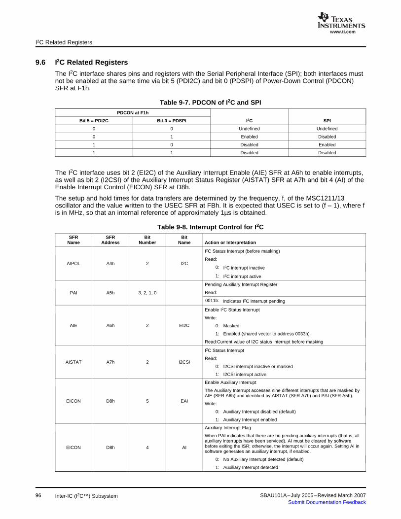
www.ti.com
9.6 I2C Related Registers
I2C Related Registers
The I2C interface shares pins and registers with the Serial Peripheral Interface (SPI); both interfaces mustnot be enabled at the same time via bit 5 (PDI2C) and bit 0 (PDSPI) of Power-Down Control (PDCON)SFR at F1h.
Table 9-7. PDCON of I2C and SPIPDCON at F1h
Bit 5 = PDI2C Bit 0 = PDSPI I2C SPI
0 0 Undefined Undefined
0 1 Enabled Disabled
1 0 Disabled Enabled
1 1 Disabled Disabled
The I2C interface uses bit 2 (EI2C) of the Auxiliary Interrupt Enable (AIE) SFR at A6h to enable interrupts,as well as bit 2 (I2CSI) of the Auxiliary Interrupt Status Register (AISTAT) SFR at A7h and bit 4 (AI) of theEnable Interrupt Control (EICON) SFR at D8h.
The setup and hold times for data transfers are determined by the frequency, f, of the MSC1211/13oscillator and the value written to the USEC SFR at FBh. It is expected that USEC is set to (f – 1), where fis in MHz, so that an internal reference of approximately 1µs is obtained.
Table 9-8. Interrupt Control for I2CSFR SFR Bit Bit
Name Address Number Name Action or Interpretation
I2C Status Interrupt (before masking)
Read:AIPOL A4h 2 I2C
0: I2C interrupt inactive
1: I2C interrupt active
Pending Auxiliary Interrupt Register
Read:PAI A5h 3, 2, 1, 0
0011b: indicates I2C interrupt pending
Enable I2C Status Interrupt
Write:
AIE A6h 2 EI2C 0: Masked
1: Enabled (shared vector to address 0033h)
Read:Current value of I2C status interrupt before masking
I2C Status Interrupt
Read:AISTAT A7h 2 I2CSI
0: I2CSI interrupt inactive or masked
1: I2CSI interrupt active
Enable Auxiliary Interrupt
The Auxiliary Interrupt accesses nine different interrupts that are masked byAIE (SFR A6h) and identified by AISTAT (SFR A7h) and PAI (SFR A5h).
EICON D8h 5 EAI Write:
0: Auxiliary Interrupt disabled (default)
1: Auxiliary Interrupt enabled
Auxiliary Interrupt Flag
When PAI indicates that there are no pending auxiliary interrupts (that is, allauxiliary interrupts have been serviced), AI must be cleared by softwarebefore exiting the ISR; otherwise, the interrupt will occur again. Setting AI inEICON D8h 4 AIsoftware generates an auxiliary interrupt, if enabled.
0: No Auxiliary Interrupt detected (default)
1: Auxiliary Interrupt detected
96 SBAU101A–July 2005–Revised March 2007Inter-IC (I2C™) SubsystemSubmit Documentation Feedback
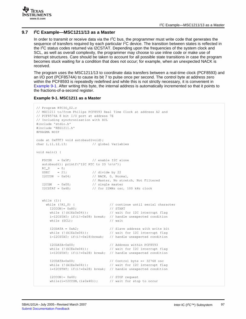
www.ti.com
9.7 I2C Example—MSC1211/13 as a Master
I2C Example—MSC1211/13 as a Master
In order to transmit or receive data via the I2C bus, the programmer must write code that generates thesequence of transfers required by each particular I2C device. The transition between states is reflected inthe I2C status codes returned via I2CSTAT. Depending upon the frequencies of the system clock andSCL, as well as overall complexity, the programmer may choose to use inline code or make use ofinterrupt structures. Care should be taken to account for all possible state transitions in case the programbecomes stuck waiting for a condition that does not occur; for example, when an unexpected NACK isreceived.
The program uses the MSC1211/13 to coordinate data transfers between a real-time clock (PCF8593) andan I/O port (PCF8574A) to cause its bit 7 to pulse once per second. The control byte at address zerowithin the PCF8593 is repeatedly redefined and while this is not strictly necessary, it is convenient inExample 9-1. After writing this byte, the internal address is automatically incremented so that it points tothe fractions-of-a-second register.
Example 9-1. MSC1211 as a Master
// Program RTCIO_02.c// MSC1211 to/from Philips PCF8593 Real Time Clock at address A2 and// PCF8574A 8 bit I/O port at address 7E// Including synchronisation with SCL#include "stdio.h"#include "REG1211.h"#PRAGMA NOIP
code at 0xFFF3 void autobaud(void);char i,i1,i2,i3; // global Variables
void main()
PDCON = 0x5F; // enable I2C aloneautobaud(); printf("I2C RTC to IO \n\n");RI_0 = 0;USEC = 21; // divide by 22I2CCON = 0x04; // NACK, 0, Normal,
// Master, No stretch, Not FilteredI2CGM = 0x00; // single masterI2CSTAT = 0x6D; // for 22MHz osc, 100 kHz clock
while (1)while (!RI_0) // continue until serial characterI2CCON|= 0x80; // STARTwhile (!(AIE&0x04)); // wait for I2C interrupt flagi=I2CSTAT; if(i!=0x08) break; // handle unexpected conditionwhile (SCL); // wait
I2CDATA = 0xA2; // Slave address with write bitwhile (!(AIE&0x04)); // wait for I2C interrupt flagi=I2CSTAT; if(i!=0x18)break; // handle unexpected condition
I2CDATA=0x00; // Address within PCF8593while (!(AIE&0x04)); // wait for I2C interrupt flagi=I2CSTAT; if(i!=0x28) break; // handle unexpected condition
I2CDATA=0x00; // Control byte => 32768 oscwhile (!(AIE&0x04)); // wait for I2C interrupt flagi=I2CSTAT; if(i!=0x28) break; // handle unexpected condition
I2CCON|= 0x40; // STOP requestwhile(i=I2CCON,(i&0x40)); // wait for stop to occur
SBAU101A–July 2005–Revised March 2007 97Inter-IC (I2C™) SubsystemSubmit Documentation Feedback
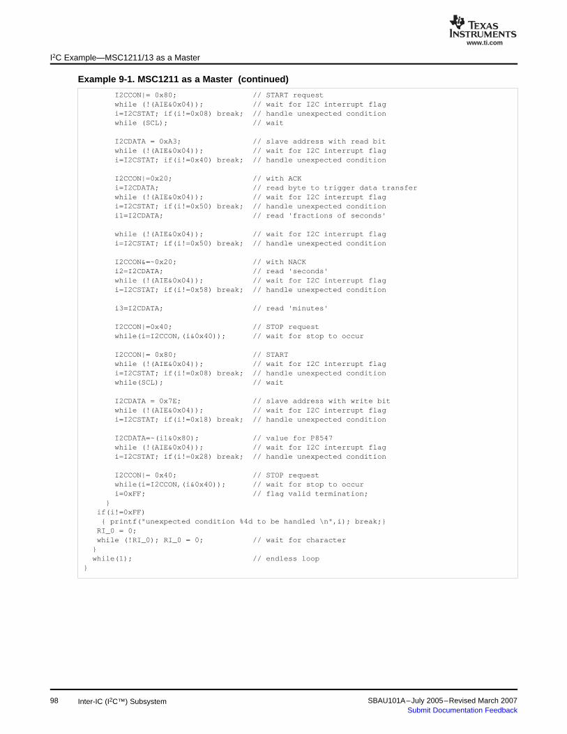
www.ti.com
I2C Example—MSC1211/13 as a Master
Example 9-1. MSC1211 as a Master (continued)
I2CCON|= 0x80; // START requestwhile (!(AIE&0x04)); // wait for I2C interrupt flagi=I2CSTAT; if(i!=0x08) break; // handle unexpected conditionwhile (SCL); // wait
I2CDATA = 0xA3; // slave address with read bitwhile (!(AIE&0x04)); // wait for I2C interrupt flagi=I2CSTAT; if(i!=0x40) break; // handle unexpected condition
I2CCON|=0x20; // with ACKi=I2CDATA; // read byte to trigger data transferwhile (!(AIE&0x04)); // wait for I2C interrupt flagi=I2CSTAT; if(i!=0x50) break; // handle unexpected conditioni1=I2CDATA; // read 'fractions of seconds'
while (!(AIE&0x04)); // wait for I2C interrupt flagi=I2CSTAT; if(i!=0x50) break; // handle unexpected condition
I2CCON&=~0x20; // with NACKi2=I2CDATA; // read 'seconds'while (!(AIE&0x04)); // wait for I2C interrupt flagi=I2CSTAT; if(i!=0x58) break; // handle unexpected condition
i3=I2CDATA; // read 'minutes'
I2CCON|=0x40; // STOP requestwhile(i=I2CCON,(i&0x40)); // wait for stop to occur
I2CCON|= 0x80; // STARTwhile (!(AIE&0x04)); // wait for I2C interrupt flagi=I2CSTAT; if(i!=0x08) break; // handle unexpected conditionwhile(SCL); // wait
I2CDATA = 0x7E; // slave address with write bitwhile (!(AIE&0x04)); // wait for I2C interrupt flagi=I2CSTAT; if(i!=0x18) break; // handle unexpected condition
I2CDATA=~(i1&0x80); // value for P8547while (!(AIE&0x04)); // wait for I2C interrupt flagi=I2CSTAT; if(i!=0x28) break; // handle unexpected condition
I2CCON|= 0x40; // STOP requestwhile(i=I2CCON,(i&0x40)); // wait for stop to occuri=0xFF; // flag valid termination;
if(i!=0xFF) printf("unexpected condition %4d to be handled \n",i); break;RI_0 = 0;while (!RI_0); RI_0 = 0; // wait for character
while(1); // endless loop
98 SBAU101A–July 2005–Revised March 2007Inter-IC (I2C™) SubsystemSubmit Documentation Feedback

www.ti.com
9.8 I2C Example—MSC1211/13 as a Slave
I2C Example—MSC1211/13 as a Slave
When operating as a slave, data may be received, transmitted, or both. In Example 9-2, two bytes arereceived from a master, and the AND and OR are sent back. To simulate the time taken for additionalcomputations encountered in most real applications, a delay is introduced to emphasize the effect of astretched clock, when the slave holds SCL low. The I2C Status Interrupt flag in AIE is set as a result of thepositive edge of SCL during the Acknowledge bit, but SCL is not stretched until the negative edge. TheSCLS bit in I2CCON must be set in order to release the SCL line, but this must not occur until the clock isbeing stretched.
The C code uses a switch statement to create a multi-way branch for each of the expected status codes.More efficient code may be created using assembler language.
Example 9-2. MSC1211/13 as a Slave
// Slave04.c// I2C master to/from slave MSC1211 at address 1110100// Returned data are functions of received data.#include "stdio.h"#include "REG1211.h"#PRAGMA NOIPcode at 0xFFF3 void autobaud(void);char i,r1=0,r2=0,t1=1,t2=2; //global Variablesint j;void delay(void) for(j=0;j<1000;j++);void release(void) while(SCL); // ensure clock is lowI2CCON|=0x02; // set clock stretch release bit
void process_data(void) t1=r1 & r2; // ANDt2=r1 | r2; // ORdelay(); // simulate additional processing time
void main() PDCON = 0x5F; // enable I2C aloneautobaud(); printf("MSC1211 as an I2C slave \n\n");RI_0 = 0;USEC = 21; // divide by 22I2CCON = 0x20; // ACK, 0, Normal, Slave, No stretch, Not FilteredI2CGM = 0x00; // General Call IgnoredI2CSTAT = 0xF4; // Master 'sees' slave at E8while (1)while (!RI_0) // continue until serial characterI2CCON|= 0x20; // ACKwhile (!(AIE&0x04)); // wait for I2C interrupt flagi=I2CSTAT; // get status and clear I2C interrupt flagswitch(i) /* slave address+W */ case 0x60 : release(); break;/* received data */ case 0x80 : r1=r2; r2=I2CDATA; release(); break;/* STOP */ case 0xA0 : break;/* slave address+R */case 0xA8 : process_data(); I2CDATA=t1; release(); break;
/* transmit data + ACK */case 0xB8 : I2CCON&=~0x20; I2CDATA=t2; release(); break;
/* transmit data + NACK */case 0xC0 : release(); break;
default :printf("Unexpected condition %4d to be handled \n",i); while(1);
RI_0 = 0;while (!RI_0); RI_0 = 0; // wait for character
SBAU101A–July 2005–Revised March 2007 99Inter-IC (I2C™) SubsystemSubmit Documentation Feedback

www.ti.com
9.9 I2C Example—MSC1211/13 as an Interrupt-Driven Slave
I2C Example—MSC1211/13 as an Interrupt-Driven Slave
In many applications, I2C communications occur via interrupts, as shown in Example 9-3. It provides thesame functional behavior as Example 9-2, except the MSC1211/13 is free to run a foreground task.
Example 9-3. MSC1211/13 as an Interrupt-Driven Slave
// Slave04i01.c - Using interrupts// I2C master to/from slave MSC1211 at address 1110100// returned data are functions of received data. Common 'release' mechanism#include "stdio.h"#include "REG1211.h"#PRAGMA NOIP
code at 0xFFF3 void autobaud(void);
char r1=0,r2=0,t1=1,t2=2; // global Variablesint j;
void delay(void) for(j=0;j<1000;j++);
void release(void) while(SCL); // ensure clock is lowI2CCON|=0x02; // set clock stretch release bit
void process_data(void) t1=r1 & r2; // ANDt2=r1 | r2; // ORdelay(); // simulate additional processing time
void Aux_Int(void) interrupt 6 using 1 char i;i=PAI; // Auxiliary Interrupt status codeif(i==3)I2CCON|= 0x20; // ACKi=I2CSTAT; // get status and clear I2C interrupt flagswitch(i)
/* slave address+W */ case 0x60 : release(); break;/* received data */ case 0x80 : r1=r2; r2=I2CDATA; release(); break;/* stop */ case 0xA0 : break;/* slave address+R */
case 0xA8 : process_data(); I2CDATA=t1; release(); break;/* transmit data + ACK */
case 0xB8 : I2CCON&=~0x20; I2CDATA=t2; release(); break;/* transmit data + NACK */
case 0xC0 : release(); break;default :printf("Unexpected condition %4d to be handled \n",i); while(1);
AI=0; // clear Auxiliary Interrupt flag
elseprintf("Unexpected interrupt %4d to be handled \n",i); while(1);
100 SBAU101A–July 2005–Revised March 2007Inter-IC (I2C™) SubsystemSubmit Documentation Feedback
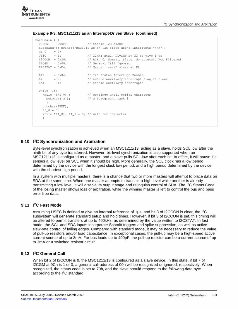
www.ti.com
9.10 I2C Synchronization and Arbitration
9.11 I2C Fast Mode
9.12 I2C General Call
I2C Synchronization and Arbitration
Example 9-3. MSC1211/13 as an Interrupt-Driven Slave (continued)
void main() PDCON = 0x5F; // enable I2C aloneautobaud(); printf("MSC1211 as an I2C slave using interrupts \n\n");RI_0 = 0;USEC = 21; // 22MHz xtal, Divide by 22 to give 1 usI2CCON = 0x20; // ACK, 0, Normal, Slave, No stretch, Not FilteredI2CGM = 0x00; // General Call IgnoredI2CSTAT = 0xF4; // Master 'sees' slave at E8
AIE = 0x04; // I2C Status Interrupt EnableAI = 0; // ensure auxiliary interrupt flag is clearEAI = 1; // enable auxiliary interrupts
while (1)while (!RI_0) // continue until serial character
putchar('a'); // a foreground task !
putchar(SBUF);RI_0 = 0;while(!RI_0); RI_0 = 0; // wait for character
Byte-level synchronization is achieved when an MSC1211/13, acting as a slave, holds SCL low after theninth bit of any byte transferred. However, bit-level synchronization is also supported when anMSC1211/13 is configured as a master, and a slave pulls SCL low after each bit. In effect, it will pause if itsenses a low level on SCL when it should be high. More generally, the SCL clock has a low perioddetermined by the device with the longest clock low period, and a high period determined by the devicewith the shortest high period.
In a system with multiple masters, there is a chance that two or more masters will attempt to place data onSDA at the same time. When one master attempts to transmit a high level while another is alreadytransmitting a low level, it will disable its output stage and relinquish control of SDA. The I2C Status Codeof the losing master shows loss of arbitration, while the winning master is left to control the bus and passerror-free data.
Assuming USEC is defined to give an internal reference of 1µs, and bit 3 of I2CCON is clear, the I2Csubsystem will generate standard setup and hold times. However, if bit 3 of I2CCON is set, this timing willbe altered to permit transfers at up to 400kHz, as determined by the value written to I2CSTAT. In fastmode, the SCL and SDA inputs incorporate Schmitt triggers and spike suppression, as well as activeslew-rate control of falling edges. Compared with standard mode, it may be necessary to reduce the valueof pull-up resistors and/or load capacitance. In exceptional cases, the pull-up may be a high-speed activecurrent source of up to 3mA. For bus loads up to 400pF, the pull-up resistor can be a current source of upto 3mA or a switched resistor circuit.
When bit 2 of I2CCON is 0, the MSC1211/13 is configured as a slave device. In this state, if bit 7 ofI2CGM at 9Ch is 1 or 0, a general call address of 00h will be recognized or ignored, respectively. Whenrecognized, the status code is set to 70h, and the slave should respond to the following data byteaccording to the I2C standard.
SBAU101A–July 2005–Revised March 2007 101Inter-IC (I2C™) SubsystemSubmit Documentation Feedback

www.ti.com
9.13 I2C 10-Bit Addressing
I2C 10-Bit Addressing
The original 7-bit addressing scheme of the I2C standard allocates addresses according to Table 9-9.
Table 9-9. Address Allocation
Most Significant Seven bits R/W Standard Meaning Extended Meaning, Where Different
0000 000 0 General call
0000 000 1 Start byte for slow devices
0000 001 x (1) Address for CBUS protocol
0000 010 x Address reserved for different protocol
0000 011 to 0000 111 x To be defined
0001 000 to 1110 111 R/W I2C device addresses
1111 0aa R/W Reserved Most significant two bits of 10-bit address
1111 1xx x Reserved
(1) x = don't care.
To increase the number of addressable devices, the I2C standard was extended to accommodate anadditional 10-bit address space. The most significant two bits are contained within addresses that wereoriginally reserved, while the remaining eight bits are provided in the following byte. The MSC1211/13neither generates nor accepts 10-bit addresses automatically. However, the 10-bit addressing protocolmay be replicated under software control to implement either a master transmitter or a slave receiver. Amaster receiver or slave transmitter cannot be implemented because the interpretation of the R/W flagprecludes transmission or reception (respectively) of the low part of the address as a data byte.
102 SBAU101A–July 2005–Revised March 2007Inter-IC (I2C™) SubsystemSubmit Documentation Feedback
Chapter 10SBAU101A–July 2005–Revised March 2007
Serial Peripheral Interface (SPI)
This chapter describes the serial peripheral interface (SPI) of the MSC121x.
Topic ........................................................................................................... Page
10.1 Description ...................................................................................... 10410.2 SPI Configuration ............................................................................. 10410.3 SPI Interrupts................................................................................... 10710.4 SPI FIFO Buffer ................................................................................ 10810.5 SPI Examples................................................................................... 111
SBAU101A–July 2005–Revised March 2007 Serial Peripheral Interface (SPI™) 103Submit Documentation Feedback
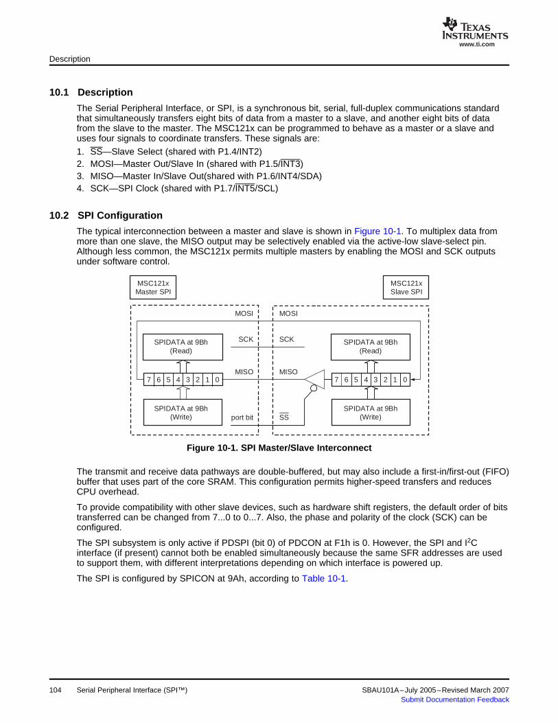
www.ti.com
10.1 Description
10.2 SPI Configuration
MSC121xMaster SPI
MSC121xSlave SPI
7 6 5 4 3 2 1 0
SPIDATA at 9Bh(Read)
SPIDATA at 9Bh(Write)
SPIDATA at 9Bh(Read)
SPIDATA at 9Bh(Write)
7 6 5 4 3 2 1 0
MOSI
SCK
MISO
MOSI
SCK
MISO
port bit SS
Description
The Serial Peripheral Interface, or SPI, is a synchronous bit, serial, full-duplex communications standardthat simultaneously transfers eight bits of data from a master to a slave, and another eight bits of datafrom the slave to the master. The MSC121x can be programmed to behave as a master or a slave anduses four signals to coordinate transfers. These signals are:
1. SS—Slave Select (shared with P1.4/INT2)2. MOSI—Master Out/Slave In (shared with P1.5/INT3)3. MISO—Master In/Slave Out(shared with P1.6/INT4/SDA)4. SCK—SPI Clock (shared with P1.7/INT5/SCL)
The typical interconnection between a master and slave is shown in Figure 10-1. To multiplex data frommore than one slave, the MISO output may be selectively enabled via the active-low slave-select pin.Although less common, the MSC121x permits multiple masters by enabling the MOSI and SCK outputsunder software control.
Figure 10-1. SPI Master/Slave Interconnect
The transmit and receive data pathways are double-buffered, but may also include a first-in/first-out (FIFO)buffer that uses part of the core SRAM. This configuration permits higher-speed transfers and reducesCPU overhead.
To provide compatibility with other slave devices, such as hardware shift registers, the default order of bitstransferred can be changed from 7...0 to 0...7. Also, the phase and polarity of the clock (SCK) can beconfigured.
The SPI subsystem is only active if PDSPI (bit 0) of PDCON at F1h is 0. However, the SPI and I2Cinterface (if present) cannot both be enabled simultaneously because the same SFR addresses are usedto support them, with different interpretations depending on which interface is powered up.
The SPI is configured by SPICON at 9Ah, according to Table 10-1.
Serial Peripheral Interface (SPI™)104 SBAU101A–July 2005–Revised March 2007Submit Documentation Feedback
www.ti.com
SPI Configuration
Table 10-1. SPICON—SPI ControlSPICON SFR 9Ah Reset Value = 00h
Bit # Name Action or Interpretation
7 SCK2 SCK Selection. SCK = SCK2:SCK1:SCK0 = 000b to 111b
6 SCK1 SPI clock frequency = fCLK/2(SCK+1). That is, fCLK/2 to fCLK/256 in powers of 2.
5 SCK0 SPI clock period = tCLK × 2(SCK+1). That is, tCLK × 2 to tCLK × 256 in powers of 2.
Enable FIFO buffer in core SRAM
4 FIFO 0: Transmit and receive pathways are double buffered
1: Circular FIFO buffer is used for to transmit and receive bytes
Sets bit order for transmit and receive
3 ORDER 0: Most significant bit first
1: Least significant bit first
SPI Master Mode
2 MSTR 0: Slave mode
1: Master mode
Serial clock phase control
1 CPHA 0: Valid data starting from half SCK period before the first edge of SCK
1: Valid data starting from the first edge of SCK
CPOL serial clock polarity
0 CPOL 0: SCK idle at logic low
1: SCK idle at logic high
Bits in Port 1 at 90h that are shared with SPI signals should be left in their default states or possiblyconfigured as inputs or CMOS outputs, depending on the signal and mode of operation.
Table 10-2. P1—Port 1 (1)
P1 SFR 90h Reset Value = FFh
Master Slave
Bit # Signal Bit Type Port Value Bit Type Port Value
4 SS 8051 or CMOS 0 or 1 8051 or input 1
8051 or CMOS or5 MOSI 1 8051 or input 1Open Drain
8051 or CMOS or6 MISO 8051 or Input 1 1Open Drain
8051 or CMOS or7 SCK 1 8051 or input 1Open Drain(1) Bits configured as open drain may require a pull-up resistor.
Table 10-3. P1DDRH—Port 1 Data Direction RegisterP1DDRH SFR AFh Reset Value = 00h
Bit # Name Action or Interpretation
7-6 P17H:P17L Port bit type:00: Standard 8051
5-4 P16H:P16L 01: CMOS output10: Open drain output3-2 P15H:P15L11: Input
1-0 P14H:P15L
SBAU101A–July 2005–Revised March 2007 Serial Peripheral Interface (SPI™) 105Submit Documentation Feedback

www.ti.com
1) SS Asserted2) First SCK Edge3) CNTIF Set (dependent on CPHA bit)4) SS Negated
SCK Cycle #
MSB 6 5 4 3 2 1 LSB
MSB 6 5 4 3 2 1 LSB
Slave CPHA = 0 Transfer in Progress
2
431
1 2 3 4 5 6 7 8
Slave CPHA = 1 Transfer in Progress
Sample Input
(CPHA = 0) Data Out
(CPHA = 1) Data Out
Sample Input
SS to Slave
SCK (CPOL = 0)
SCK (CPOL = 1)
SPI Configuration
Figure 10-2. SPI Clock/Data Timing
CPHA and CPOL alter the phase of the data and the polarity of the clock to suit various applications.
Data to be transmitted are written to the SPI Data Register (SPIDATA at 9Bh), which is then passed to thedouble-buffered SPI transmit interface. Similarly, data that have been received are read via this SFR fromthe double-buffered SPI receive interface. Data are routed through a FIF0 buffer of up to 128 bytes if bit 4of SPICON at 9Ah is set.
Table 10-4. SPIDATA—SPI Data RegisterSPIDATA SFR 9Bh Reset Value = 00h
Bit # Name Action or Interpretation
7-0 SPIDATA Write/Read: Data to be transmitted by, or received from, the Serial Peripheral Interface.
106 Serial Peripheral Interface (SPI™) SBAU101A–July 2005–Revised March 2007Submit Documentation Feedback
www.ti.com
10.3 SPI Interrupts
SPI Interrupts
When an SPI interrupt is active and enabled, the MSC121x CPU jumps to location 0033h. The interruptservice routine (ISR) may read the Pending Auxiliary Interrupt Register (PAI at A5h) to establish thesource of the interrupt. The number returned is 3 for the SPI receiver, and 4 for the SPI transmitter,assuming that higher priority auxiliary interrupts have not occurred.
AI (bit 4 of EICON), must be cleared within the ISR when no further auxiliary interrupts are pending.Setting AI in software generates an Auxiliary Interrupt, if enabled, but if there are no pending interrupts thePending Auxiliary Interrupt vector in PIA at A5h will read as 0.
When the FIFO buffer is disabled, the transmit interrupt flag will be set whenever the SPI transmitter isempty and the receiver interrupt flag will be set whenever there is a received byte to read. Writing toSPIDATA clears the transmit interrupt flag, if previously set. Similarly, reading SPIDATA clears the receiveinterrupt flag, if previously set. Because of the bit-synchronous nature of the SPI, a byte is only receivedwhen one is transmitted. Consequently, if a master expects a reply that is dependent upon the byte it sentto a slave, it must ignore the first byte returned and transmit dummy bytes to receive subsequent replybytes.
Table 10-5. SPI Interrupts Have Highest Priority and Jump to Address 0033hBit Name Abbreviation Name of Related SFR Abbreviation Address
Enable Auxiliary Interrupt EAI Enable Interrupt Control EICON.5 D8h
Auxiliary Interrupt Flag AI Enable Interrupt Control EICON.4 D8h
Enable SPI Transmit interrupt ESPIT Auxiliary Interrupt Enable AIE.3 A6h
SPIT AISTAT.3 A7hSPI Transmit Interrupt Status Flag Auxiliary Interrupt Status RegisterESPIT AIPOL.3 A4h
Enable SPI Receive Interrupt ESPIR Auxiliary Interrupt Enable AIE.2 A6h
SPIR AISTAT.2 A7hSPI Receiver Interrupt Status Flag Auxiliary Interrupt Status RegisterESPIR AIPOL.2 A4h
Table 10-6. PAI—Pending Auxiliary Interrupt RegisterPAI SFR A5h Reset Value = 00h
Bit # Name Interpretation When Read
7-4 — Return 0
Auxiliary Interrupt Status0000: No Pending Auxiliary IRQ0001: Digital Low-Voltage or Hardware Breakpoint IRQ Pending0010: Analog Low-Voltage IRQ Pending0011: SPI Receive IRQ Pending or I2C Status Interrupt Pending3-0 PAI3-PAI00100: SPI Transmit IRQ Pending0101: One Millisecond System Timer IRQ Pending0110: Analog-to-Digital Conversion IRQ Pending0111: Accumulator IRQ Pending1000: One Second System Timer IRQ Pending
SBAU101A–July 2005–Revised March 2007 Serial Peripheral Interface (SPI™) 107Submit Documentation Feedback
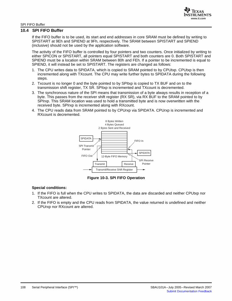
www.ti.com
10.4 SPI FIFO Buffer
8 Bytes Written4 Bytes Queued
2 Bytes Sent and Received
12−Byte FIFO Memory
SPIDATA
SPIDATA
FIFO In
FIFO Out
SPI TransmitPointer
SPI ReceivePointerTransmit Receive
Transmit/Receive Shift Register
SPI FIFO Buffer
If the FIFO buffer is to be used, its start and end addresses in core SRAM must be defined by writing toSPISTART at 9Eh and SPIEND at 9Fh, respectively. The SRAM between SPISTART and SPIEND(inclusive) should not be used by the application software.
The activity of the FIFO buffer is controlled by four pointers and two counters. Once initialized by writing toeither SPICON or SPISTART, all pointers equal SPISTART and both counters are 0. Both SPISTART andSPIEND must be a location within SRAM between 80h and FEh. If a pointer to be incremented is equal toSPIEND, it will instead be set to SPISTART. The registers are changed as follows:
1. The CPU writes data to SPIDATA, which is copied to SRAM pointed to by CPUtxp. CPUtxp is thenincremented along with TXcount. The CPU may write further bytes to SPIDATA during the followingsteps.
2. Txcount is no longer 0 and the byte pointed to by SPItxp is copied to TX BUF and on to thetransmission shift register, TX SR. SPItxp is incremented and TXcount is decremented.
3. The synchronous nature of the SPI means that transmission of a byte always results in reception of abyte. This passes from the receiver shift register (RX SR), via RX BUF to the SRAM pointed to bySPIrxp. This SRAM location was used to hold a transmitted byte and is now overwritten with thereceived byte. SPIrxp is incremented along with RXcount.
4. The CPU reads data from SRAM pointed to by CPUrxp via SPIDATA. CPUrxp is incremented andRXcount is decremented.
Figure 10-3. SPI FIFO Operation
Special conditions:1. If the FIFO is full when the CPU writes to SPIDATA, the data are discarded and neither CPUtxp nor
TXcount are altered.2. If the FIFO is empty and the CPU reads from SPIDATA, the value returned is undefined and neither
CPUrxp nor RXcount are altered.
Serial Peripheral Interface (SPI™)108 SBAU101A–July 2005–Revised March 2007Submit Documentation Feedback
www.ti.com
SPI FIFO Buffer
Table 10-7. SPISTART—SPI Buffer Start AddressSPISTART SFR 9Eh Reset Value = 80h
Bit # Name Action or Interpretation
7 — Always 1
Write: The start address of the circular FIFO buffer, somewhere within SRAM from 80h to FEh. The valuemust be less than SPIEND. The FIFO resides between SPISTART and SPIEND, inclusive. Writing to
SPISTART SPISTART initializes all the FIFO pointers and counters.
6-0 CPUwrp = SPItxp = CPUrdp = SPIrxp = SPISTART, and TXcount = RXcount = 0.
Read: The current value of the CPU Transmit Pointer (CPUwrp). This is where the next byte for transmissionSPITP is placed when the CPU writes to SPIDATA. Writing to SPIDATA increments the transmit counter and
increments CPUwrp, unless that would make CPUtxp equal to the SPI Receive pointer (SPIrxp).
Table 10-8. SPISEND—SPI Buffer End AddressSPIEND SFR 9Fh Reset Value = 80h
Bit # Name Action or Interpretation
7 — Always 1
Write: The end address of the circular FIFO buffer, somewhere within SRAM from 80h to FFh. The valueSPIEND must be greater than SPISTART. The FIFO resides between SPISTART and SPIEND inclusive.6-0 Read: The current value of the CPU Receive Pointer (CPUrxp). This indicates where the next byte will be
SPIRP taken from as the CPU reads SPIDATA. Reading SPIDATA decrements the receive counter and incrementsthe SPI Receive Pointer (SPIrxp) unless the receive counter is zero.
To sustain data transfers via the SPI while minimizing CPU overhead, the FIFO buffer will usually be filledand emptied in bursts by the application software. To coordinate this type of activity, the SPI ReceiveControl register (SPIRCON at 9Ch) and the SPI Transmit Control register (SPITCON at 9Dh) allowinterrupts to be determined by the amount of data in the buffer. A receive interrupt can be set to occurwhen 2N or more bytes have arrived, and a transmit interrupt when 2N or less remain to be transmitted,where N is between 0 and 7.
The receive buffer may be flushed by writing a '1' to RXFLUSH (bit 7 of SPIRCON), which causes CPUrxpto be set equal to SPIrxp, and RXcount to 0.
The transmit buffer may be flushed by writing a '1' to TXFLUSH (bit 7 of SPITCON), which causes CPUtxpto be set equal to SPItxp, and TXcount to 0.
SBAU101A–July 2005–Revised March 2007 Serial Peripheral Interface (SPI™) 109Submit Documentation Feedback
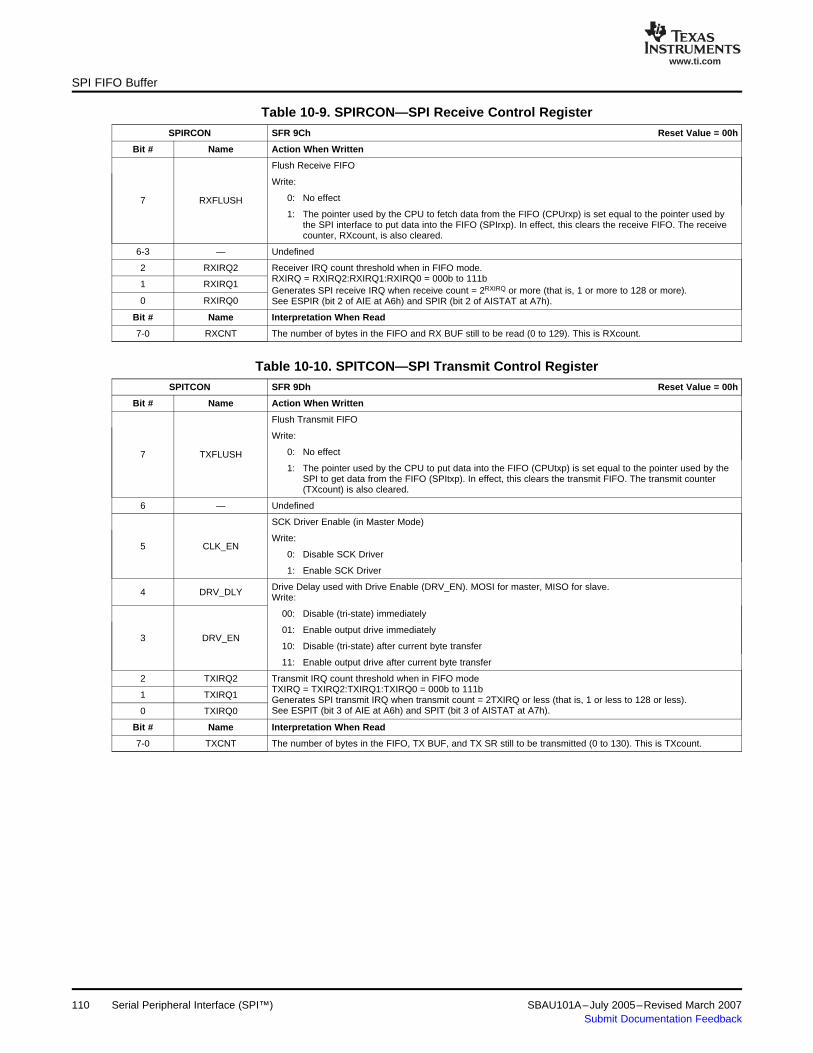
www.ti.com
SPI FIFO Buffer
Table 10-9. SPIRCON—SPI Receive Control RegisterSPIRCON SFR 9Ch Reset Value = 00h
Bit # Name Action When Written
Flush Receive FIFO
Write:
0: No effect7 RXFLUSH
1: The pointer used by the CPU to fetch data from the FIFO (CPUrxp) is set equal to the pointer used bythe SPI interface to put data into the FIFO (SPIrxp). In effect, this clears the receive FIFO. The receivecounter, RXcount, is also cleared.
6-3 — Undefined
2 RXIRQ2 Receiver IRQ count threshold when in FIFO mode.RXIRQ = RXIRQ2:RXIRQ1:RXIRQ0 = 000b to 111b
1 RXIRQ1Generates SPI receive IRQ when receive count = 2RXIRQ or more (that is, 1 or more to 128 or more).
0 RXIRQ0 See ESPIR (bit 2 of AIE at A6h) and SPIR (bit 2 of AISTAT at A7h).
Bit # Name Interpretation When Read
7-0 RXCNT The number of bytes in the FIFO and RX BUF still to be read (0 to 129). This is RXcount.
Table 10-10. SPITCON—SPI Transmit Control RegisterSPITCON SFR 9Dh Reset Value = 00h
Bit # Name Action When Written
Flush Transmit FIFO
Write:
0: No effect7 TXFLUSH
1: The pointer used by the CPU to put data into the FIFO (CPUtxp) is set equal to the pointer used by theSPI to get data from the FIFO (SPItxp). In effect, this clears the transmit FIFO. The transmit counter(TXcount) is also cleared.
6 — Undefined
SCK Driver Enable (in Master Mode)
Write:5 CLK_EN
0: Disable SCK Driver
1: Enable SCK Driver
Drive Delay used with Drive Enable (DRV_EN). MOSI for master, MISO for slave.4 DRV_DLY Write:
00: Disable (tri-state) immediately
01: Enable output drive immediately3 DRV_EN
10: Disable (tri-state) after current byte transfer
11: Enable output drive after current byte transfer
2 TXIRQ2 Transmit IRQ count threshold when in FIFO modeTXIRQ = TXIRQ2:TXIRQ1:TXIRQ0 = 000b to 111b
1 TXIRQ1 Generates SPI transmit IRQ when transmit count = 2TXIRQ or less (that is, 1 or less to 128 or less).See ESPIT (bit 3 of AIE at A6h) and SPIT (bit 3 of AISTAT at A7h).0 TXIRQ0
Bit # Name Interpretation When Read
7-0 TXCNT The number of bytes in the FIFO, TX BUF, and TX SR still to be transmitted (0 to 130). This is TXcount.
Serial Peripheral Interface (SPI™)110 SBAU101A–July 2005–Revised March 2007Submit Documentation Feedback

www.ti.com
10.5 SPI Examples
SPI Examples
Two examples are shown using the SPI. Example 10-1 shows a simple, polled environment. Example10-2 shows an SPI program using interrupts.
Example 10-1. SPI, Simple, Polled Environment
// File SPIpolled.c - outputs and receives bytes via SPI// MSC1211 EVM Switches 1:On SW3-12345678 SW5-12345678// 0:Off 11110111 11110000#include <Reg1211.h>#include <stdio.h>sbit RedLed = P3^4; // RED LED on EVMsbit YellowLed = P3^5; // Yellow LED on EVMsbit SlaveSelect = P1^0; // avoids onboard SPI devicescode at 0xFFF3 void autobaud(void);
unsigned char SPIoutin(unsigned char n)while (!(AIE & 0x08)) RedLed=!RedLed; //wait for TX emptySPIDATA=n; // outputwhile (!(AIE & 0x04)) YellowLed=!YellowLed; //wait for RXreturn SPIDATA; // input
void main(void) data unsigned char i,j=0x41;AIE=0; // No interruptsPDCON&=~0x01; // turns on SPIP1DDRH=0x40; // CMOS output for P1.7P1DDRL=0x01; // CMOS output for P1.4SPICON=0xC4; // Divide 128, FIFO off, msb, masterSPITCON=0x28; // SCK driver onSlaveSelect=1;autobaud();printf("Simple polled (loopback) SPI\n");RI_0 = 0; // Clear received flag in UARTwhile(1)while(!RI_0)
RedLed=YellowLed=0;SlaveSelect=0;i=SPIoutin(j);SlaveSelect=1;putchar(i);
RI_0 = 0; // any character to pausewhile(!RI_0); // wait for characterj=SBUF0; // get characterRI_0 = 0; // continue
A burst of characters is written to the FIFO in every second, and with MOSI and MISO joined together,they are read back by the CPU whenever the number of received characters is 16 or more. If the burstsize is less than 16, two or more seconds will be needed to trigger a receive interrupt.
SBAU101A–July 2005–Revised March 2007 Serial Peripheral Interface (SPI™) 111Submit Documentation Feedback
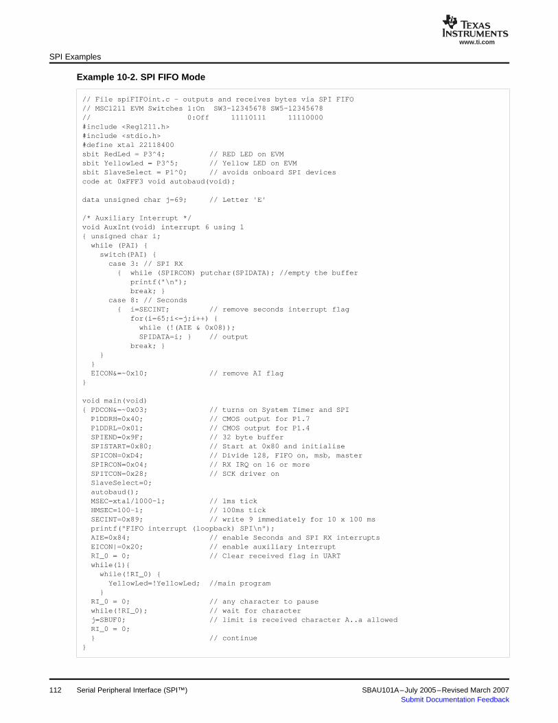
www.ti.com
SPI Examples
Example 10-2. SPI FIFO Mode
// File spiFIFOint.c - outputs and receives bytes via SPI FIFO// MSC1211 EVM Switches 1:On SW3-12345678 SW5-12345678// 0:Off 11110111 11110000#include <Reg1211.h>#include <stdio.h>#define xtal 22118400sbit RedLed = P3^4; // RED LED on EVMsbit YellowLed = P3^5; // Yellow LED on EVMsbit SlaveSelect = P1^0; // avoids onboard SPI devicescode at 0xFFF3 void autobaud(void);
data unsigned char j=69; // Letter 'E'
/* Auxiliary Interrupt */void AuxInt(void) interrupt 6 using 1 unsigned char i;while (PAI) switch(PAI)
case 3: // SPI RX while (SPIRCON) putchar(SPIDATA); //empty the buffer
printf("\n");break;
case 8: // Seconds i=SECINT; // remove seconds interrupt flag
for(i=65;i<=j;i++) while (!(AIE & 0x08));SPIDATA=i; // output
break;
EICON&=~0x10; // remove AI flag
void main(void) PDCON&=~0x03; // turns on System Timer and SPIP1DDRH=0x40; // CMOS output for P1.7P1DDRL=0x01; // CMOS output for P1.4SPIEND=0x9F; // 32 byte bufferSPISTART=0x80; // Start at 0x80 and initialiseSPICON=0xD4; // Divide 128, FIFO on, msb, masterSPIRCON=0x04; // RX IRQ on 16 or moreSPITCON=0x28; // SCK driver onSlaveSelect=0;autobaud();MSEC=xtal/1000-1; // 1ms tickHMSEC=100-1; // 100ms tickSECINT=0x89; // write 9 immediately for 10 x 100 msprintf("FIFO interrupt (loopback) SPI\n");AIE=0x84; // enable Seconds and SPI RX interruptsEICON|=0x20; // enable auxiliary interruptRI_0 = 0; // Clear received flag in UARTwhile(1)while(!RI_0)
YellowLed=!YellowLed; //main program
RI_0 = 0; // any character to pausewhile(!RI_0); // wait for characterj=SBUF0; // limit is received character A..a allowedRI_0 = 0; // continue
112 Serial Peripheral Interface (SPI™) SBAU101A–July 2005–Revised March 2007Submit Documentation Feedback
Chapter 11SBAU101A–July 2005–Revised March 2007
Timers and Counters
This chapter describes the MSC121x timers and counters.
Topic ........................................................................................................... Page
11.1 Description ...................................................................................... 11411.2 Timer/Counters 0 and 1 ..................................................................... 11411.3 Timer/Counter 2 ............................................................................... 11911.4 Example Program Using Timers 0, 1, and 2 ......................................... 124
SBAU101A–July 2005–Revised March 2007 Timers and Counters 113Submit Documentation Feedback
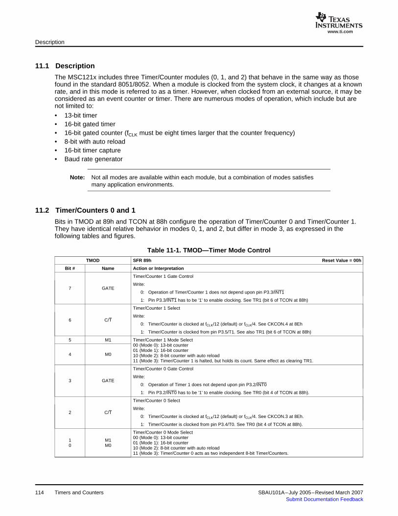
www.ti.com
11.1 Description
11.2 Timer/Counters 0 and 1
Description
The MSC121x includes three Timer/Counter modules (0, 1, and 2) that behave in the same way as thosefound in the standard 8051/8052. When a module is clocked from the system clock, it changes at a knownrate, and in this mode is referred to as a timer. However, when clocked from an external source, it may beconsidered as an event counter or timer. There are numerous modes of operation, which include but arenot limited to:
• 13-bit timer• 16-bit gated timer• 16-bit gated counter (fCLK must be eight times larger that the counter frequency)• 8-bit with auto reload• 16-bit timer capture• Baud rate generator
Note: Not all modes are available within each module, but a combination of modes satisfiesmany application environments.
Bits in TMOD at 89h and TCON at 88h configure the operation of Timer/Counter 0 and Timer/Counter 1.They have identical relative behavior in modes 0, 1, and 2, but differ in mode 3, as expressed in thefollowing tables and figures.
Table 11-1. TMOD—Timer Mode ControlTMOD SFR 89h Reset Value = 00h
Bit # Name Action or Interpretation
Timer/Counter 1 Gate Control
Write:7 GATE
0: Operation of Timer/Counter 1 does not depend upon pin P3.3/INT1
1: Pin P3.3/INT1 has to be '1' to enable clocking. See TR1 (bit 6 of TCON at 88h)
Timer/Counter 1 Select
Write:6 C/T
0: Timer/Counter is clocked at fCLK/12 (default) or fCLK/4. See CKCON.4 at 8Eh
1: Timer/Counter is clocked from pin P3.5/T1. See also TR1 (bit 6 of TCON at 88h)
5 M1 Timer/Counter 1 Mode Select00 (Mode 0): 13-bit counter01 (Mode 1): 16-bit counter
4 M0 10 (Mode 2): 8-bit counter with auto reload11 (Mode 3): Timer/Counter 1 is halted, but holds its count. Same effect as clearing TR1.
Timer/Counter 0 Gate Control
Write:3 GATE
0: Operation of Timer 1 does not depend upon pin P3.2/INT0
1: Pin P3.2/INT0 has to be '1' to enable clocking. See TR0 (bit 4 of TCON at 88h).
Timer/Counter 0 Select
Write:2 C/T
0: Timer/Counter is clocked at fCLK/12 (default) or fCLK/4. See CKCON.3 at 8Eh.
1: Timer/Counter is clocked from pin P3.4/T0. See TR0 (bit 4 of TCON at 88h).
Timer/Counter 0 Mode Select00 (Mode 0): 13-bit counter1 M1 01 (Mode 1): 16-bit counter0 M0 10 (Mode 2): 8-bit counter with auto reload11 (Mode 3): Timer/Counter 0 acts as two independent 8-bit Timer/Counters.
Timers and Counters114 SBAU101A–July 2005–Revised March 2007Submit Documentation Feedback

www.ti.com
Timer/Counters 0 and 1
Table 11-2. TCON—Timer/Counter ControlTCON SFR 88h Reset Value = 00h
Bit # Name Action or Interpretation
Timer 1 (Interrupt) Overflow Flag
Read:
0: No Overflow
1: Timer 1 reached the maximum count and changed to 07 TF1
Write:
0: Clear flag
1: Set flag and generate interrupt request if unmasked
Cleared in software by writing 0, or cleared automatically as the processor jumps to the ISR at 001Bh
Timer 1 Run Control
Write:6 TR1
0: Timer 1 cannot be clocked
1: Timer 1 may be clocked
Timer 0 (Interrupt) Overflow Flag
Read:
0: No Overflow
1: Timer 0 reached maximum count and changed to 05 TF0
Write:
0: Clear flag
1: Set flag and generate interrupt request if unmasked
Cleared in software by writing 0, or cleared automatically as the processor jumps to the ISR at 000Bh
Timer 0 Run Control
Write:4 TR0
0: Timer 0 cannot be clocked
1: Timer 0 may be clocked
Interrupt 1 Edge Detect
If INT1 is edge-sensitive because IT1 = 1, IE1 is set when a negative edge is detected. It is cleared when the3 (1) IE1CPU jumps to the ISR at 0013h or by writing 0 in software. If IT1 = 0, IE1 is set when the INT1 pin is low, andcleared when the INT1 pin is high.
Interrupt 1 type select
Write:2 IT1
0: INT1 is sensitive to a low level
1: INT1 is sensitive to a negative (falling) edge
Interrupt 0 edge select
If INT0 is edge-sensitive because IT0 = 1, IE0 is set when a negative edge is detected. It is cleared when the1 IE0CPU jumps to the ISR at 0013h or by writing 0 in software. If IT0 = 0, IE1 is set when the INT0 pin is low, andcleared when the INT0 pin is high.
Interrupt 0 type select
Write:0 (1) IT0
0: INT0 is sensitive to a low level
1: INT0 is sensitive to a negative (falling) edge
(1) Bit 0 to bit 3 of TCON are not associated with the operation of any Timer/Counter.
SBAU101A–July 2005–Revised March 2007 Timers and Counters 115Submit Documentation Feedback
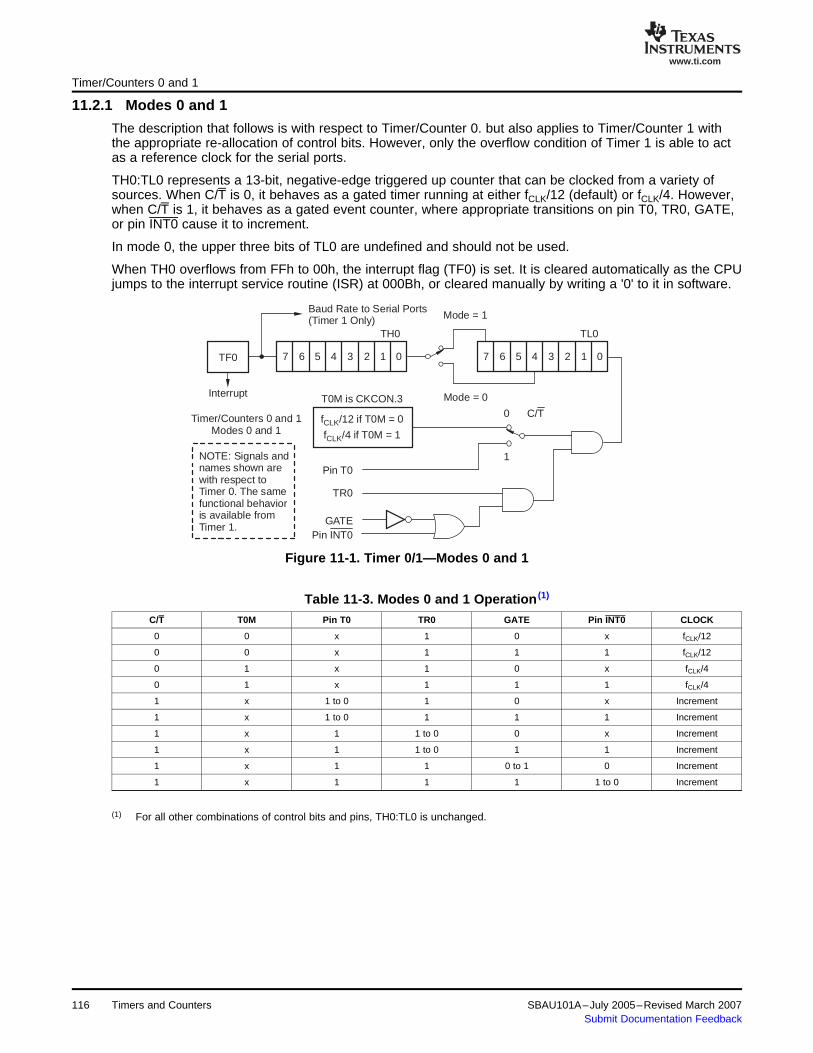
www.ti.com
11.2.1 Modes 0 and 1
7 6 5 4 3 2 1 0
Baud Rate to Serial Ports(Timer 1 Only) Mode = 1
T0M is CKCON.3
fCLK/12 if T0M = 0
fCLK/4 if T0M = 1
Mode = 0
0
1
TH0
Pin T0
TR0
GATEPin INT0
TF0
Interrupt
Timer/Counters 0 and 1Modes 0 and 1
TL0
7 6 5 4 3 2 1 0
NOTE: Signals andnames shown arewith respect toTimer 0. The samefunctional behavioris available fromTimer 1.
C/T
Timer/Counters 0 and 1
The description that follows is with respect to Timer/Counter 0. but also applies to Timer/Counter 1 withthe appropriate re-allocation of control bits. However, only the overflow condition of Timer 1 is able to actas a reference clock for the serial ports.
TH0:TL0 represents a 13-bit, negative-edge triggered up counter that can be clocked from a variety ofsources. When C/T is 0, it behaves as a gated timer running at either fCLK/12 (default) or fCLK/4. However,when C/T is 1, it behaves as a gated event counter, where appropriate transitions on pin T0, TR0, GATE,or pin INT0 cause it to increment.
In mode 0, the upper three bits of TL0 are undefined and should not be used.
When TH0 overflows from FFh to 00h, the interrupt flag (TF0) is set. It is cleared automatically as the CPUjumps to the interrupt service routine (ISR) at 000Bh, or cleared manually by writing a '0' to it in software.
Figure 11-1. Timer 0/1—Modes 0 and 1
Table 11-3. Modes 0 and 1 Operation (1)
C/T T0M Pin T0 TR0 GATE Pin INT0 CLOCK
0 0 x 1 0 x fCLK/12
0 0 x 1 1 1 fCLK/12
0 1 x 1 0 x fCLK/4
0 1 x 1 1 1 fCLK/4
1 x 1 to 0 1 0 x Increment
1 x 1 to 0 1 1 1 Increment
1 x 1 1 to 0 0 x Increment
1 x 1 1 to 0 1 1 Increment
1 x 1 1 0 to 1 0 Increment
1 x 1 1 1 1 to 0 Increment
(1) For all other combinations of control bits and pins, TH0:TL0 is unchanged.
Timers and Counters116 SBAU101A–July 2005–Revised March 2007Submit Documentation Feedback

www.ti.com
11.2.2 Mode 2
Baud Rate to Serial Ports(Timer 1 Only)
T0M is CKCON.3
fCLK/12 if T0M = 0
fCLK/4 if T0M = 1
0
1Pin T0
TR0
GATEPin INT0
TF0Interrupt
Reload
Timer/Counters 0 and 1Mode 2
TL0
7 6 5 4 3 2 1 0
TH0
7 6 5 4 3 2 1 0
NOTE: Signals andnames shown arewith respect toTimer 0. The samefunctional behavioris available fromTimer 1.
C/T
11.2.3 Mode 3
T0M is CKCON.3
fCLK/12 if T0M = 0
fCLK/4 if T0M = 1
0 C/T
1Pin T0
TR0
GATEPin INT0
TF1Interrupt
TR1Timer 0Mode 3
TL0
TF0Interrupt
7 6 5 4 3 2 1 0
TH0
7 6 5 4 3 2 1 0
NOTE: TH0 triggersthe interruptassociated withTimer 1. WhenTimer 0 is in Mode3, Timer 1 can stillbe used in Modes0, 1, and 2, butwithout an overflowflag.
Timer/Counters 0 and 1
The description that follows is with respect to Timer/Counter 0, but applies to Timer/Counter 1 withappropriate re-allocation of control bits. However, only the overflow condition of Timer 1 is able to act as areference clock for the serial ports.
Figure 11-2. Timer 0/1—Mode 2
TL0 represents an 8-bit, negative-edge triggered counter that is reloaded from TH0 as it overflows. It maybe from clocked from a variety of sources as described for modes 0 and 1.
The behavior of Timer/Counter 0 in mode 3 is not the same as that of Timer/Counter 1 because theinterrupt flag usually associated with Timer 1 is controlled by TH0.
Figure 11-3. Timer 0—Mode 3
TL0 is an 8-bit timer or counter that is clocked and gated in a manner similar to Mode 0. TH0 must beclocked from the same source but is gated only by control bit TR1. Without TR1 and TF1, Timer 1 can stillbe used for baud rate generation.
SBAU101A–July 2005–Revised March 2007 Timers and Counters 117Submit Documentation Feedback
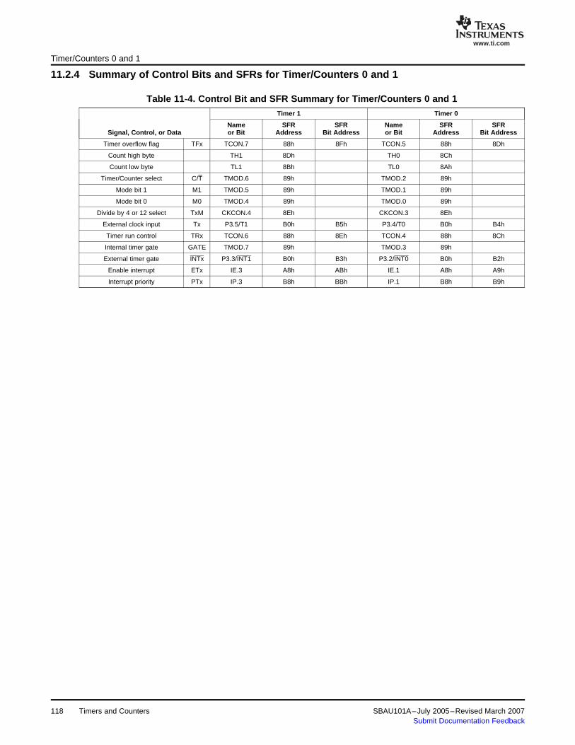
www.ti.com
11.2.4 Summary of Control Bits and SFRs for Timer/Counters 0 and 1
Timer/Counters 0 and 1
Table 11-4. Control Bit and SFR Summary for Timer/Counters 0 and 1Timer 1 Timer 0
Name SFR SFR Name SFR SFRSignal, Control, or Data or Bit Address Bit Address or Bit Address Bit Address
Timer overflow flag TFx TCON.7 88h 8Fh TCON.5 88h 8Dh
Count high byte TH1 8Dh TH0 8Ch
Count low byte TL1 8Bh TL0 8Ah
Timer/Counter select C/T TMOD.6 89h TMOD.2 89h
Mode bit 1 M1 TMOD.5 89h TMOD.1 89h
Mode bit 0 M0 TMOD.4 89h TMOD.0 89h
Divide by 4 or 12 select TxM CKCON.4 8Eh CKCON.3 8Eh
External clock input Tx P3.5/T1 B0h B5h P3.4/T0 B0h B4h
Timer run control TRx TCON.6 88h 8Eh TCON.4 88h 8Ch
Internal timer gate GATE TMOD.7 89h TMOD.3 89h
External timer gate INTx P3.3/INT1 B0h B3h P3.2/INT0 B0h B2h
Enable interrupt ETx IE.3 A8h ABh IE.1 A8h A9h
Interrupt priority PTx IP.3 B8h BBh IP.1 B8h B9h
118 Timers and Counters SBAU101A–July 2005–Revised March 2007Submit Documentation Feedback

www.ti.com
11.3 Timer/Counter 2
Timer/Counter 2
Timer/Counter 2 consists of the register pair TH2:TL2, which act as a 16-bit, negative-edge triggered upcounter. The associated register pair, RCAPH:RCAPL, may either capture the current value of TH2:TL2 orprovide a reload value according to the mode of operation selected by bits in T2CON at C8h.
Table 11-5. T2CON—Timer 2 ControlT2CON SFR C8h Reset Value = 00h
Bit # Name Action or Interpretation
Timer 2 Overflow Flag
Read:
0: No Overflow1:Timer 2 reached maximum count of FFFFh and overflowed to 0. It is not cleared automatically as the7 TF2 processor jumps to the ISR at 002Bh.
Write:
0: Clear flag if set1: Set overflow flag and generate interrupt if enabled
Timer 2 External Flag
This flag is set by a high-to-low transition on pin P1.1/T2EX with EXEN2 previously set.6 EXF2 Write:
0: Clear flag if set1: Set overflow flag and generate interrupt if enabled
Receive Clock Select
Write:5 RCLK
0 (or 1): Timer 1 (or 2) overflow rate determines the receiver baud rate for USART0 in modes 1 or 3. Setting thisbit forces Timer 2 into a 16-bit auto-reload mode where the reference clock is fCLK/2 or pin P1.0/T2.USART 1 can only be clocked from Timer/Counter 1.
Transmit Clock Select
Write:4 TCLK
0 (or 1): Timer 1 (or 2) overflow rate determines the transmitter baud rate for USART0 in serial modes 1 or 3.Setting this bit forces Timer 2 into a 16-bit auto-reload mode where the reference clock is fCLK/2 or pinP1.0/T2. USART 1 can only be clocked from Timer/Counter 1.
Timer 2 External Enable
Write:3 EXEN2
0: Ignore negative edges on pin P1.1/T2EX1: Negative edge on pin P1.1/T2EX sets EXF2 and causes capture or reload depending on the operating modeof Timer/Counter
Timer 2 Run Control
Write:2 TR20: Timer 2 cannot be clocked1: Timer 2 may be clocked
Timer 2 Counter/Timer Select
Write:1 C/T20: Counter/Timer is clocked at fCLK/12 (default) or fCLK/4; or fCLK/2 in Baud Rate mode1: Counter/Timer is clocked from pin P1.0/T2
Capture/Reload Select
Write:
0: Auto-reloads when Timer/Counter 2 overflows, or on high-to-low transitions of P1.1/T2EX, if EXEN2 = 10 CP/RL21:Captures on high-to-low transitions of P1.1/T2EX, if EXEN2 = 1
Note that if either RCLK or TCLK = 1, CP/RL2 does not function and Timer/Counter 2 auto-reloads following anoverflow.
SBAU101A–July 2005–Revised March 2007 Timers and Counters 119Submit Documentation Feedback

www.ti.com
11.3.1 16-Bit Timer/Counter with Optional Capture
T2M is CKCON.5
fCLK/12 if T2M = 0
fCLK/4 if T2M = 1
1−to−0Edge
Detection
0 C/T2
1Pin T2
TR2
EXF2
TF2
Timer 2Interrupt
Capture
PinT2EX
EXEN2
Timer/Counter 216−Bit with Capture
RCAP2H
TH2
7 6 5 4 3 2 1 0 7 6 5 4 3 2 1 0
RCAP2L
TL2
7 6 5 4 3 2 1 0 7 6 5 4 3 2 1 0
Timer/Counter 2
To select this mode, RCLK, TCLK, and CP/RL2 in T2CON must all be '0'.
Control bit TR2 is active high and enables either an internal clock or an external clock on pin P1.0/T2,depending on the state of C/T2. Specifically, when C/T2 is '0', TH2:TL2 is a gated timer running at eitherfCLK /12 (default) or fCLK/4. However, when C/T2 is '1', it is a gated event counter.
Figure 11-4. Timer/Counter 2—16-Bit with Capture
As TH2:TL2 overflows from FFFFh to 0000h, the interrupt flag (TF2) is set; this flag must be cleared insoftware. If interrupt enables ET2 and EA (bits 5 and 7, respectively, of IE at A8h) are both '1', the CPUjumps to the ISR at 002Bh. Writing a '1' to TF2 causes an interrupt, if it is enabled.
A negative-edge on pin P1.1/T2EX when control bit EXEN2 is '1' causes the current value of TH2:TL2 tobe copied into capture registers RCAP2H:RCAP2L and sets the interrupt flag (EXF2). This flag is ORedwith TF2 and may cause a Timer2 interrupt in a manner similar to TF2. EXF2 has to be cleared insoftware and writing a '1' to it causes an interrupt, if it is enabled.
Timers and Counters120 SBAU101A–July 2005–Revised March 2007Submit Documentation Feedback
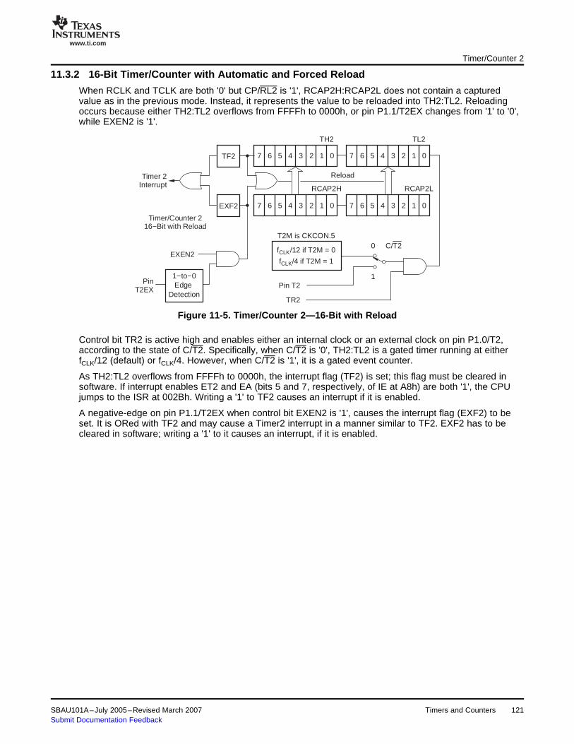
www.ti.com
11.3.2 16-Bit Timer/Counter with Automatic and Forced Reload
T2M is CKCON.5
fCLK/12 if T2M = 0
fCLK/4 if T2M = 1
1−to−0Edge
Detection
0
1Pin T2
TR2
EXF2
TF2
Timer 2Interrupt
PinT2EX
EXEN2
Timer/Counter 216−Bit with Reload
RCAP2H
Reload
TH2
7 6 5 4 3 2 1 0 7 6 5 4 3 2 1 0
RCAP2L
TL2
7 6 5 4 3 2 1 0 7 6 5 4 3 2 1 0
C/T2
Timer/Counter 2
When RCLK and TCLK are both '0' but CP/RL2 is '1', RCAP2H:RCAP2L does not contain a capturedvalue as in the previous mode. Instead, it represents the value to be reloaded into TH2:TL2. Reloadingoccurs because either TH2:TL2 overflows from FFFFh to 0000h, or pin P1.1/T2EX changes from '1' to '0',while EXEN2 is '1'.
Figure 11-5. Timer/Counter 2—16-Bit with Reload
Control bit TR2 is active high and enables either an internal clock or an external clock on pin P1.0/T2,according to the state of C/T2. Specifically, when C/T2 is '0', TH2:TL2 is a gated timer running at eitherfCLK/12 (default) or fCLK/4. However, when C/T2 is '1', it is a gated event counter.
As TH2:TL2 overflows from FFFFh to 0000h, the interrupt flag (TF2) is set; this flag must be cleared insoftware. If interrupt enables ET2 and EA (bits 5 and 7, respectively, of IE at A8h) are both '1', the CPUjumps to the ISR at 002Bh. Writing a '1' to TF2 causes an interrupt if it is enabled.
A negative-edge on pin P1.1/T2EX when control bit EXEN2 is '1', causes the interrupt flag (EXF2) to beset. It is ORed with TF2 and may cause a Timer2 interrupt in a manner similar to TF2. EXF2 has to becleared in software; writing a '1' to it causes an interrupt, if it is enabled.
SBAU101A–July 2005–Revised March 2007 Timers and Counters 121Submit Documentation Feedback
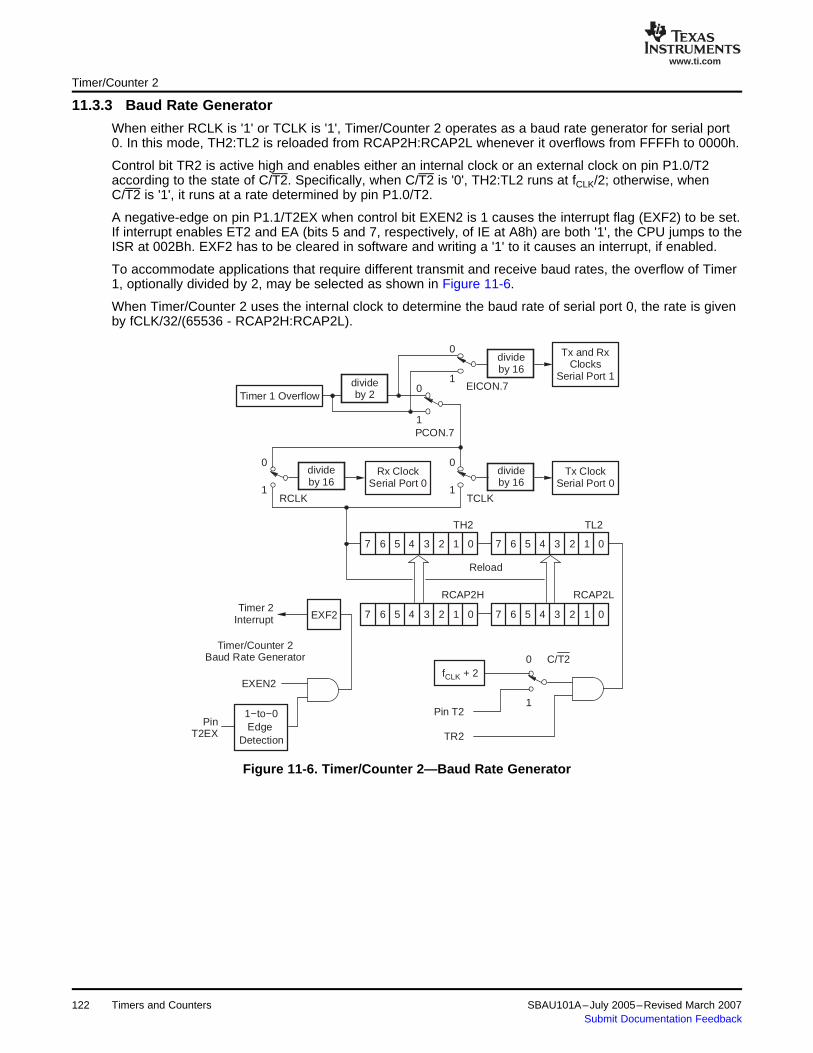
www.ti.com
11.3.3 Baud Rate Generator
fCLK + 2
1−to−0Edge
Detection
0
1Pin T2
TR2
EXF2
Rx ClockSerial Port 0
Timer 2Interrupt
PinT2EX
EXEN2
Timer/Counter 2Baud Rate Generator
RCAP2H
Reload
0
1
0
1
1
0
TH2
7 6 5 4 3 2 1 0 7 6 5 4 3 2 1 0
RCAP2L
TL2
7 6 5 4 3 2 1 0 7 6 5 4 3 2 1 0
Timer 1 Overflow
RCLK TCLK
Tx ClockSerial Port 0
0
1divideby 2
divideby 16
divideby 16
divideby 16
EICON.7
PCON.7
Tx and RxClocks
Serial Port 1
C/T2
Timer/Counter 2
When either RCLK is '1' or TCLK is '1', Timer/Counter 2 operates as a baud rate generator for serial port0. In this mode, TH2:TL2 is reloaded from RCAP2H:RCAP2L whenever it overflows from FFFFh to 0000h.
Control bit TR2 is active high and enables either an internal clock or an external clock on pin P1.0/T2according to the state of C/T2. Specifically, when C/T2 is '0', TH2:TL2 runs at fCLK/2; otherwise, whenC/T2 is '1', it runs at a rate determined by pin P1.0/T2.
A negative-edge on pin P1.1/T2EX when control bit EXEN2 is 1 causes the interrupt flag (EXF2) to be set.If interrupt enables ET2 and EA (bits 5 and 7, respectively, of IE at A8h) are both '1', the CPU jumps to theISR at 002Bh. EXF2 has to be cleared in software and writing a '1' to it causes an interrupt, if enabled.
To accommodate applications that require different transmit and receive baud rates, the overflow of Timer1, optionally divided by 2, may be selected as shown in Figure 11-6.
When Timer/Counter 2 uses the internal clock to determine the baud rate of serial port 0, the rate is givenby fCLK/32/(65536 - RCAP2H:RCAP2L).
Figure 11-6. Timer/Counter 2—Baud Rate Generator
Timers and Counters122 SBAU101A–July 2005–Revised March 2007Submit Documentation Feedback
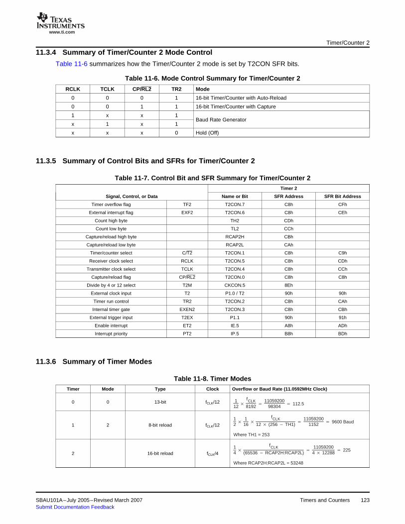
www.ti.com
11.3.4 Summary of Timer/Counter 2 Mode Control
11.3.5 Summary of Control Bits and SFRs for Timer/Counter 2
11.3.6 Summary of Timer Modes
112
fCLK8192
11059200
98304 112.5
12
116
fCLK12 (256 TH1)
11059200
1152 9600 Baud
Where TH1 = 253
14
fCLK(65536 RCAP2H:RCAP2L)
110592004 12288
225
Where RCAP2H:RCAP2L = 53248
Timer/Counter 2
Table 11-6 summarizes how the Timer/Counter 2 mode is set by T2CON SFR bits.
Table 11-6. Mode Control Summary for Timer/Counter 2
RCLK TCLK CP/RL2 TR2 Mode
0 0 0 1 16-bit Timer/Counter with Auto-Reload
0 0 1 1 16-bit Timer/Counter with Capture
1 x x 1Baud Rate Generator
x 1 x 1
x x x 0 Hold (Off)
Table 11-7. Control Bit and SFR Summary for Timer/Counter 2Timer 2
Signal, Control, or Data Name or Bit SFR Address SFR Bit Address
Timer overflow flag TF2 T2CON.7 C8h CFh
External interrupt flag EXF2 T2CON.6 C8h CEh
Count high byte TH2 CDh
Count low byte TL2 CCh
Capture/reload high byte RCAP2H CBh
Capture/reload low byte RCAP2L CAh
Timer/counter select C/T2 T2CON.1 C8h C9h
Receiver clock select RCLK T2CON.5 C8h CDh
Transmitter clock select TCLK T2CON.4 C8h CCh
Capture/reload flag CP/RL2 T2CON.0 C8h C8h
Divide by 4 or 12 select T2M CKCON.5 8Eh
External clock input T2 P1.0 / T2 90h 90h
Timer run control TR2 T2CON.2 C8h CAh
Internal timer gate EXEN2 T2CON.3 C8h CBh
External trigger input T2EX P1.1 90h 91h
Enable interrupt ET2 IE.5 A8h ADh
Interrupt priority PT2 IP.5 B8h BDh
Table 11-8. Timer ModesTimer Mode Type Clock Overflow or Baud Rate (11.0592MHz Clock)
0 0 13-bit fCLK/12
1 2 8-bit reload fCLK/12
2 16-bit reload fCLK/4
SBAU101A–July 2005–Revised March 2007 Timers and Counters 123Submit Documentation Feedback

www.ti.com
11.4 Example Program Using Timers 0, 1, and 2
Example Program Using Timers 0, 1, and 2
In Example 11-1, the red and yellow LEDs on the MSC1210 evaluation module are associated withoverflow interrupts from Timers 0 and 2, respectively. Serial port 0 is repeatedly tested for receipt of anycharacter at a baud rate of 9600, as determined by Timer 1. The character is echoed and TF2 is set togenerate an additional interrupt.
The red LED is on for one second and then off for one second, while the yellow LED flashes at half thisrate. Initially, the LEDs light at the same moment, but each received character causes an extra call(Timer2Int), which produces an increasing visible phase shift between the flashing of the LEDs.
fCLK is the same frequency as the external (crystal) oscillator, unless the System Clock Divider SFR(SYSCLK at C7h) is present and active. SYSCLK is provided in the MSC1211/12/13/14 with a defaultvalue that causes no division of the external clock.
Example 11-1. Program Using Timers 0, 1, and 2
// File Timer012b.c - Timer 0 in 13-bit mode// Timer 1 in 8-bit reload and Timer 2 in releoad// MSC1210 EVM Switches 1:On SW3-12345678 SW6-12345678// 0:Off 11110111 11110000#include <Reg1210.h>#include <stdio.h>#define fclk 11059200#define BAUD 9600#define limit 225sbit RedLed = P3^4; // RED LED on EVMsbit YellowLed = P3^5; // Yellow LED on EVM
data unsigned int i=1, j=1;
void Timer0Int(void) interrupt 1 using 1 if(!--i) i=limit; YellowLed=!YellowLed;
void Timer2Int(void) interrupt 5 using 1 if(!--j) j=limit; RedLed=!RedLed;TF2=0; // remove overflow flag
void main(void) CKCON=0x20; // Timer 2 at fclk/4; Timers 0,1 at fclk/12PCON =0x30; // SMOD = 0TMOD =0x20; // Timer 1 Auto reload; Timer 0 13-bitTCON =0x50; // TR1 and TR0 are 1TH1 =256-fclk/32/12/BAUD; // Timer 1 reload valueT2CON=0x04; // TR2 is 1, and Timer 2 is auto-reloadRCAP2=65536-fclk/4/limit;SCON0=0x52; // Asynchronous and enabled, TI_0=1, RI_0=0while(!RI_0); // wait for key pressprintf("\nMSC1210 Timer 0 in mode 0, Timer 1 in mode 2");printf("\n Timer 2 in 16-bit auto reload\n");IE =0xA2; // EA ET2 and ET1 enabledwhile(1)while(!RI_0); // wait for key pressSBUF0=SBUF0; // echoTF2=1; // Force Timer 2 interruptRI_0=0;
124 Timers and Counters SBAU101A–July 2005–Revised March 2007Submit Documentation Feedback
Chapter 12SBAU101A–July 2005–Revised March 2007
Serial Ports (USART0 and USART1)
This chapter describes the serial ports of the MSC121x.
Topic ........................................................................................................... Page
12.1 Description ...................................................................................... 12612.2 Control Bits in SCON0 and SCON1 ..................................................... 12612.3 Pin and Interrupt Assignments........................................................... 12712.4 Timer/Counters 1 and 2 Baud Rate Generation .................................... 12712.5 Mode 0—8-Bit Synchronous .............................................................. 12912.6 Mode 1—10-Bit Asynchronous........................................................... 13012.7 Modes 2 and 3—11-Bit Asynchronous ................................................ 13112.8 Multiprocessor Communications........................................................ 13212.9 Example Program............................................................................. 132
SBAU101A–July 2005–Revised March 2007 Serial Ports (USART0 and USART1) 125Submit Documentation Feedback

www.ti.com
12.1 Description
12.2 Control Bits in SCON0 and SCON1
Description
The MSC121x has two serial ports. Both may be configured in almost the same variety of synchronous orasynchronous modes and clocked via fCLK, the overflow from Timer/Counter 1 or Timer/Counter 2. USARTstands for Universal Synchronous/Asynchronous Receiver/Transmitter.
Each port has a control register and a data register, referenced as SCON0 at 98h and SBUF0 at 99h forserial port 0 and as SCON1 at C0h and SBUF1 at C1h for serial port 1.
Table 12-1. SCON0 and SCON1—Serial Port 0 and Serial Port 1 ControlSCON0 SFR 98h
SCON1 SFR C0h Reset Value = 00h
Action or Interpretation
Bit # Name0 Name1 Mode SM0 SM1 SM2 Function Length Rate (1)
0 0 0 0 Synchronous 8 fCLK /12
0 0 0 1 Synchronous 8 fCLK /47 SM0_0 SM0_1
0 Asynchronous 101 0 1 Timer (2)
1 (3) Asynchronous 10
0 Asynchronous 116 SM1_0 SM1_1 2 1 0 (2SMOD/64) × fCLK
(4)Asynchronous1 (5) 11(Multiprocessor)
3 1 1 0 Asynchronous 115 SM2_0 SM2_1 Timer (2)Asynchronous3 1 1 1 (5) 11(Multiprocessor)
Receive Enable
Write:4 REN_0 REN_1
0: receive shift register is disabled
1: receive shift register is enabled (for mode 0, RI = 0 is also required)
Ninth Transmission Bit State3 TB8_0 TB8_1
The state of the ninth bit to be transmitted in modes 2 and 3
Ninth Received Bit State2 RB8_0 RB8_1 The state of the ninth bit received in modes 2 and 3. In mode 1, when SM2 = 0, RB8_0 is the state of the stop
bit. RB8_0 is not used in mode 0.
TI_0 Transmitter Interrupt Flag
This bit is set when the transmit buffer has been completely shifted out. In mode 0, this occurs at the end of the1 TI_0 TI_1eighth data bit, while in all other modes it is set at the beginning of the STOP bit. This flag must be manuallycleared by software and can be set in software to cause an interrupt.
RI_0 Receiver Interrupt Flag
This bit indicates that a byte has been received in the input shift register. In mode 0, it is set at the end of the0 RI_0 RI_1 eighth data bit; in mode 1, after the last sample of the incoming stop bit; and in modes 2 and 3, after the last
sample of the ninth data bit. This bit must be manually cleared by software and can be set in software to causean interrupt.
(1) If IDLE (bit 7 of PCON at 87h) is set, the CPU, Timer/Counters 0,1 and 2, and both serial ports will freeze until there is anauxiliary interrupt or external wake-up (see AIE at A6h, EICON at D8h and EWU at C6h).
(2) In modes 1 and 3, serial port 0 may be clocked by Timer/Counter 1 or Timer/Counter 2, as determined by RCLK and TCLK (seeT2CON at C8h); whereas serial port 1 may be clocked only by Timer/Counter 1.
(3) In mode 1 with SM2 = 1, RI is activated only if a valid stop bit is received.(4) For USART0, SMOD0 is bit 7 of PCON at 87h. For USART1, SMOD1 is bit 7 of EICON at D8h.(5) In modes 2 and 3 with SM2 = 1, RI is activated only if the ninth received data bit is 1.
126 Serial Ports (USART0 and USART1) SBAU101A–July 2005–Revised March 2007Submit Documentation Feedback
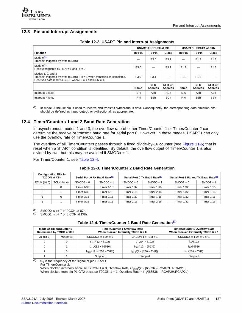
www.ti.com
12.3 Pin and Interrupt Assignments
12.4 Timer/Counters 1 and 2 Baud Rate Generation
Pin and Interrupt Assignments
Table 12-2. USART Pin and Interrupt AssignmentsUSART 0 : SBUF0 at 99h USART 1 : SBUF1 at C1h
Function Rx Pin Tx Pin Clock Rx Pin Tx Pin Clock
Mode 0 (1)— P3.0 P3.1 — P1.2 P1.3Transmit triggered by write to SBUF
Mode 0 (1)P3.0 — P3.1 P1.2 — P1.3Receive triggered by REN = 1 and RI = 0
Modes 1, 2, and 3Transmit triggered by write to SBUF; TI = 1 when transmission completed. P3.0 P3.1 — P1.2 P1.3 —Received data read via SBUF when RI = 1 and REN = 1.
SFR SFR Bit SFR SFR BitName Address Address Name Address Address
Interrupt Enable IE.4 A8h ACh IE.6 A8h AEh
Interrupt Priority IP.4 B8h BCh IP.6 B8h BEh
(1) In mode 0, the Rx pin is used to receive and transmit synchronous data. Consequently, the corresponding data direction bitsshould be defined as input, output, or bidirectional, as appropriate.
In asynchronous modes 1 and 3, the overflow rate of either Timer/Counter 1 or Timer/Counter 2 candetermine the receive or transmit baud rate for serial port 0. However, in these modes, USART1 can onlyuse the overflow rate of Timer/Counter 1.
The overflow of all Timer/Counters passes through a fixed divide-by-16 counter (see Figure 11-6) that isreset when a START condition is identified. By default, the overflow output of Timer/Counter 1 is alsodivided by two, but this may be avoided if SMODx = 1.
For Timer/Counter 1, see Table 12-4.
Table 12-3. Timer/Counter 2 Baud Rate GenerationConfiguration Bits in
T2CON at C8h Serial Port 0 Rx Baud Rate (1) Serial Port 0 Tx Baud Rate (1) Serial Port 1 Rx and Tx Baud Rate (2)
RCLK (bit 5) TCLK (bit 4) SMOD0 = 0 SMOD0 = 1 SMOD0 = 0 SMOD0 = 1 SMOD1 = 0 SMOD1 = 1
0 0 Timer 1/32 Timer 1/16 Timer 1/32 Timer 1/16 Timer 1/32 Timer 1/16
0 1 Timer 1/32 Timer 1/16 Timer 2/16 Timer 2/16 Timer 1/32 Timer 1/16
1 0 Timer 2/16 Timer 2/16 Timer 1/32 Timer 1/16 Timer 1/32 Timer 1/16
1 1 Timer 2/16 Timer 2/16 Timer 2/16 Timer 2/16 Timer 1/32 Timer 1/16
(1) SMOD0 is bit 7 of PCON at 87h.(2) SMOD1 is bit 7 of EICON at D8h.
Table 12-4. Timer/Counter 1 Baud Rate Generation (1)
Mode of Timer/Counter 1 Timer/Counter 1 Overflow Rate Timer/Counter 1 Overflow RateDetermined by TMOD at 89h When Clocked Internally TMOD.6 = 0 When Clocked Externally TMOD.6 = 1
M1 (bit 5) M0 (bit 4) CKCON.4 = T1M = 0 CKCON.4 = T1M = 1 CKCON.4 = T1M = 0 or 1
0 0 fCLK/(12 × 8192) fCLK/(4 × 8192) fT1/8192
0 1 fCLK/(12 × 65536) fCLK/(12 × 65536) fT1/65536
1 0 fCLK/(12 × [256 – TH1]) fCLK/(4 × [256 – TH1]) fT1/(256 – TH1)
1 1 Stopped Stopped Stopped(1) fT1 is the frequency of the signal at pin P3.5/T1.
For Timer/Counter 2:When clocked internally because T2CON.1 = 0, Overflow Rate = fCLK/(2 × [65536 – RCAP2H:RCAP2L]).When clocked from pin P1.0/T2 because T2CON.1 = 1, Overflow Rate = fT2/(65536 – RCAP2H:RCAP2L).
SBAU101A–July 2005–Revised March 2007 Serial Ports (USART0 and USART1) 127Submit Documentation Feedback
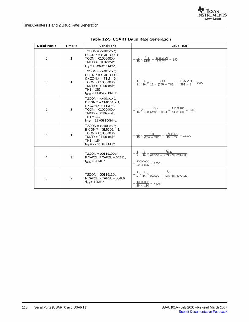
www.ti.com
116
fT18192
19660800131072
150
12
116
fCLK12 (256 TH1)
11059200384 3
9600
116
fCLK4 (256 TH1)
1105920064 144
1200
116
fT1(256 TH1)
2211840016 72
19200
12
116
fCLK(65536 RCAP2H:RCAP2L)
2500000032 325
2404
12
116
fT2(65536 RCAP2H:RCAP2L)
1000000016 130
4808
Timer/Counters 1 and 2 Baud Rate Generation
Table 12-5. USART Baud Rate Generation
Serial Port # Timer # Conditions Baud Rate
T2CON = xx00xxxxb;PCON.7 = SMOD0 = 1;
0 1 TCON = 01000000b;TMOD = 0100xxxxb;fT1 = 19.660800MHz.
T2CON = xx00xxxxb;PCON.7 = SMOD0 = 0;CKCON.4 = T1M = 0;
0 1 TCON = 01000000b;TMOD = 0010xxxxb;TH1 = 253;fCLK = 11.059200MHz
T2CON = xx00xxxxb;EICON.7 = SMOD1 = 1;CKCON.4 = T1M = 1;
1 1 TCON = 01000000b;TMOD = 0010xxxxb;TH1 = 112;fCLK = 11.059200MHz
T2CON = xx00xxxxb;EICON.7 = SMOD1 = 1;TCON = 01000000b;1 1 TMOD = 0110xxxxb;TH1 = 184;fT1 = 22.118400MHz
T2CON = 00110100b;0 2 RCAP2H:RCAP2L = 65211;
fCLK = 25MHz
T2CON = 00110110b;0 2 RCAP2H:RCAP2L = 65406
;fT2 = 10MHz
128 Serial Ports (USART0 and USART1) SBAU101A–July 2005–Revised March 2007Submit Documentation Feedback

www.ti.com
12.5 Mode 0—8-Bit Synchronous
clk
mem_ale
rxd0_in
rxd0_out
txd0
TI
RI
D0 D1 D2 D3 D4 D5 D6 D7
clk
mem_ale
rxd0_in
rxd0_out
txd0
TI
RI
D0 D1 D2 D3 D4 D5 D6 D7
Mode 0—8-Bit Synchronous
In mode 0, serial data are either received or transmitted eight bits at a time in a synchronous fashion withrespect to a shared input/output pin and a common clock output. Reception is triggered when REN = 1and RI = 0, while transmission is triggered by a write to SBUF. If SM2 is '0', the clock runs at fCLK/12;otherwise, it runs at fCLK/4, as shown in Figure 12-1 and Figure 12-2. There are no start or stop bits in thismode.
RI is set three fCLK cycles after the eighth bit has been received, and TI is set three fCLK cycles after theeighth bit has been transmitted. This is true when SM2 = 0, but the delays change to four fCLK cycles whenSM2 = 1.
Figure 12-1. Synchronous Receive at fCLK/4
Figure 12-2. Synchronous Transmit at fCLK/4
SBAU101A–July 2005–Revised March 2007 Serial Ports (USART0 and USART1) 129Submit Documentation Feedback
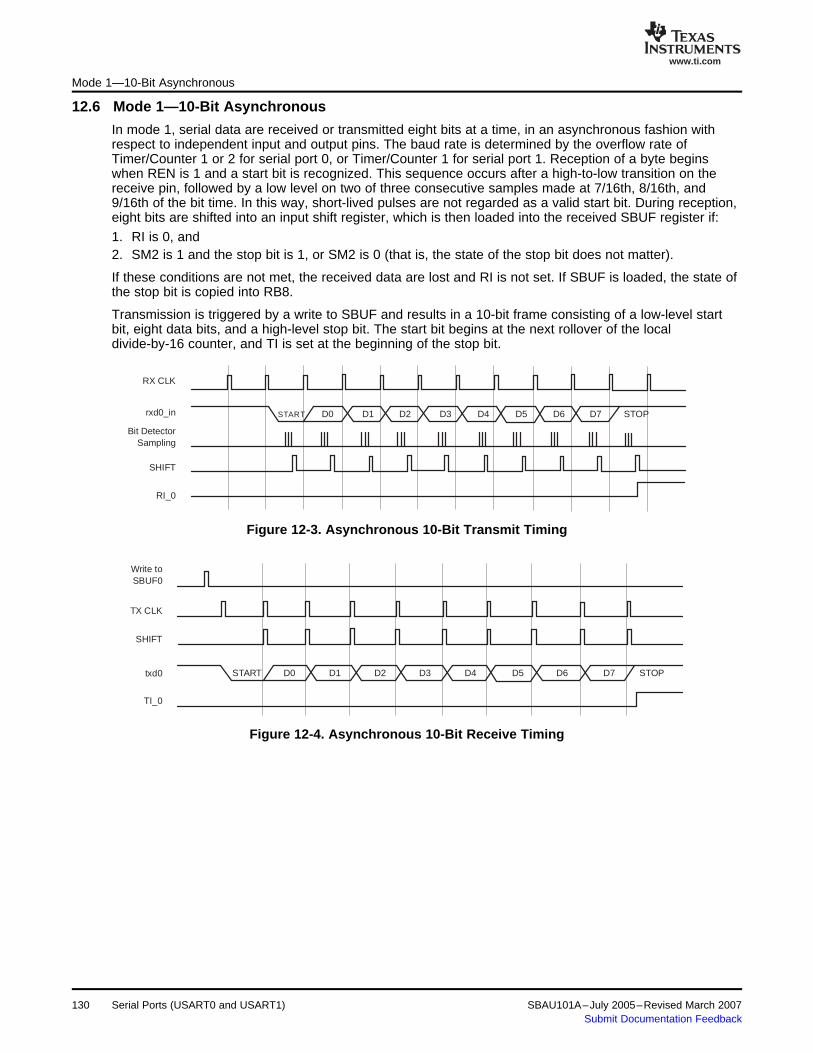
www.ti.com
12.6 Mode 1—10-Bit Asynchronous
RX CLK
rxd0_in
Bit DetectorSampling
SHIFT
START STOPD0 D1 D2 D3 D4 D5 D6 D7
RI_0
Write toSBUF0
TX CLK
SHIFT
txd0 START STOPD0 D1 D2 D3 D4 D5 D6 D7
TI_0
Mode 1—10-Bit Asynchronous
In mode 1, serial data are received or transmitted eight bits at a time, in an asynchronous fashion withrespect to independent input and output pins. The baud rate is determined by the overflow rate ofTimer/Counter 1 or 2 for serial port 0, or Timer/Counter 1 for serial port 1. Reception of a byte beginswhen REN is 1 and a start bit is recognized. This sequence occurs after a high-to-low transition on thereceive pin, followed by a low level on two of three consecutive samples made at 7/16th, 8/16th, and9/16th of the bit time. In this way, short-lived pulses are not regarded as a valid start bit. During reception,eight bits are shifted into an input shift register, which is then loaded into the received SBUF register if:
1. RI is 0, and2. SM2 is 1 and the stop bit is 1, or SM2 is 0 (that is, the state of the stop bit does not matter).
If these conditions are not met, the received data are lost and RI is not set. If SBUF is loaded, the state ofthe stop bit is copied into RB8.
Transmission is triggered by a write to SBUF and results in a 10-bit frame consisting of a low-level startbit, eight data bits, and a high-level stop bit. The start bit begins at the next rollover of the localdivide-by-16 counter, and TI is set at the beginning of the stop bit.
Figure 12-3. Asynchronous 10-Bit Transmit Timing
Figure 12-4. Asynchronous 10-Bit Receive Timing
130 Serial Ports (USART0 and USART1) SBAU101A–July 2005–Revised March 2007Submit Documentation Feedback
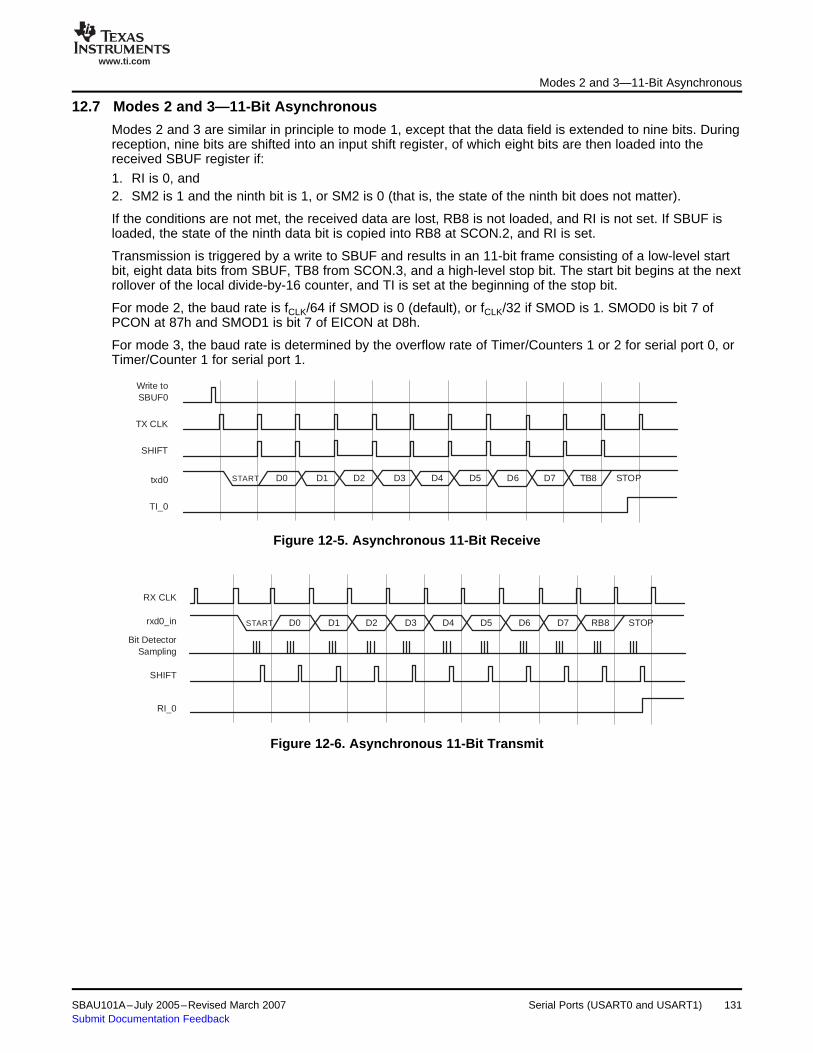
www.ti.com
12.7 Modes 2 and 3—11-Bit Asynchronous
TX CLK
Write toSBUF0
SHIFT
START STOPD0 D1 D2 D3 D4 D5 D6 D7 TB8
TI_0
txd0
RX CLK
rxd0_in
Bit DetectorSampling
SHIFT
START STOPD0 D1 D2 D3 D4 D5 D6 D7 RB8
RI_0
Modes 2 and 3—11-Bit Asynchronous
Modes 2 and 3 are similar in principle to mode 1, except that the data field is extended to nine bits. Duringreception, nine bits are shifted into an input shift register, of which eight bits are then loaded into thereceived SBUF register if:
1. RI is 0, and2. SM2 is 1 and the ninth bit is 1, or SM2 is 0 (that is, the state of the ninth bit does not matter).
If the conditions are not met, the received data are lost, RB8 is not loaded, and RI is not set. If SBUF isloaded, the state of the ninth data bit is copied into RB8 at SCON.2, and RI is set.
Transmission is triggered by a write to SBUF and results in an 11-bit frame consisting of a low-level startbit, eight data bits from SBUF, TB8 from SCON.3, and a high-level stop bit. The start bit begins at the nextrollover of the local divide-by-16 counter, and TI is set at the beginning of the stop bit.
For mode 2, the baud rate is fCLK/64 if SMOD is 0 (default), or fCLK/32 if SMOD is 1. SMOD0 is bit 7 ofPCON at 87h and SMOD1 is bit 7 of EICON at D8h.
For mode 3, the baud rate is determined by the overflow rate of Timer/Counters 1 or 2 for serial port 0, orTimer/Counter 1 for serial port 1.
Figure 12-5. Asynchronous 11-Bit Receive
Figure 12-6. Asynchronous 11-Bit Transmit
SBAU101A–July 2005–Revised March 2007 Serial Ports (USART0 and USART1) 131Submit Documentation Feedback

www.ti.com
12.8 Multiprocessor Communications
12.9 Example Program
Serial Port 0 Receiver Software Buffer Serial Port 1 Transmitter
Serial Port 0 Transmitter Serial Port 1 Receiver
Multiprocessor Communications
For serial ports operating in modes 2 or 3 with control bit SM2 = 1, the RI flag will only be set if the ninthbit of a received data field is 1. In this way, a byte may cause an interrupt only when the ninth data bit is 1.
In a multiprocessor system, when a master chooses to send a block of data to one of several slaves, itfirst transmits an address with the ninth data bit (from SCON.3) at 1. Assuming all slaves initially haveSM2 set, each will be interrupted because RI is set; however, only the one matching the address willchange its SM2 bit to 0. Thereafter, data bytes with the ninth data bit at 0 will be ignored by unaddressedslaves, but cause an interrupt in the addressed slave.
In Example 12-1, the program has both serial ports operating in mode 1, where asynchronous 8-bit dataare preceded by a start bit and succeeded by a stop bit. Since both ports have SM2 = 1 (SCONx.5 = 1),the RI flags are set only if a valid stop bit is received.
Serial port 0 is configured to receive and transmit characters at 9600 baud using Timer/Counter 2,whereas serial port 1 has a non-standard rate of approximately 21 baud using Timer1. Charactersreceived on serial port 0 are buffered in software and presented for transmission via serial port 1. It isassumed that serial port 1 transmitter is looped back to serial port 1 receiver. Characters received at serialport 1 are copied back to serial port 0, as shown in Figure 12-7.
Figure 12-7. Serial Port with Software Buffer
When implemented in a software development environment together with an MSC1210EVM, the user isable to type characters at the PC keyboard and see the same characters on the download window, butwith a noticeable delay. The yellow LED will flicker as characters are passed at 21 baud on pin P1.2.
The baud rate of serial port 1 is slow, so the buffer may quickly fill up if keys are typed too rapidly.Impending overflow is indicated by the red LED.
Example 12-1. Serial Port with Software Buffer Code
// File Serial01buf.c - Using serial ports 0 and 1 with a buffer// MSC1210 EVM Switches 1:On SW3-12345678 SW6-12345678// 0:Off 11110111 11110000#include <Reg1210.h>#define xtal 11059200#define BAUD 9600#define limit 8sbit RedLed = P3^4; // RED LED on EVMsbit YellowLed = P3^5; // Yellow LED on EVM// Join J4 pins 2 and 3 on EVM for loopbackvoid main(void) data unsigned char i=limit, j=limit,n=0; // empty bufferidata unsigned char buffer[limit];SCON0=0x70; // Serial Port 0 mode 1 (10 bit asyn.)SCON1=0x72; // Serial Port 1 mode 1 (10 bit asyn.) TI => emptyRI_0 = RI_1 = 0; // clear received flagsCKCON=0x10; // Timer 1 at fclk/4EICON=0x80; // SMOD1 = 1TCON =0x40; // TR1 is 1TMOD =0x00; // Timer1 13-bit. Baud = xtal/(16*4*8192)=21.1T2CON=0x34; // Timer 2 is rate generator and enabledRCAP2=65536-xtal/32/BAUD;
132 Serial Ports (USART0 and USART1) SBAU101A–July 2005–Revised March 2007Submit Documentation Feedback
www.ti.com
Example Program
Example 12-1. Serial Port with Software Buffer Code (continued)
while(1)if (RI_0) // wait for key press
if (n<limit) // put character into bufferif (++i>limit) i=0; // wrap 'on' pointerbuffer[i]=SBUF0; // save save charactern++; // increment count
if (n>(limit-2)) RedLed=0; // show impending overflowRI_0=0; // remove receive flag
if (TI_1) // Is serial Port 2 Tx empty ?if (n) // Is buffer not empty ?if (++j>limit) j=0; // wrap 'off' pointerTI_1=0; // clear transmit finished flagSBUF1=buffer[j]; // send charactern--; // decrement count
else RedLed=1; // turn off overflow LED
if (RI_1) // is serial port 1 Rx full ?SBUF0=SBUF1; // copy Rx port 1 to Tx port 0RI_1=0;
YellowLed=!RXD1; // monitor serial port 1 bit stream
SBAU101A–July 2005–Revised March 2007 Serial Ports (USART0 and USART1) 133Submit Documentation Feedback

www.ti.com
Serial Ports (USART0 and USART1)134 SBAU101A–July 2005–Revised March 2007Submit Documentation Feedback

Chapter 13SBAU101A–July 2005–Revised March 2007
Interrupts
This chapter describes the MSC121x interrupts.
Topic ........................................................................................................... Page
13.1 Description ...................................................................................... 13613.2 Standard and Extended Interrupts ...................................................... 13713.3 Auxiliary Interrupt Sources................................................................ 13913.4 Multiple Interrupts ............................................................................ 14013.5 Example of Multiple and Nested Interrupts .......................................... 14013.6 Example of Wake Up from Idle ........................................................... 143
SBAU101A–July 2005–Revised March 2007 Interrupts 135Submit Documentation Feedback

www.ti.com
13.1 Description
Description
The MSC121x extends the interrupt sources provided by the 8051 architecture in two ways. First, theMSC121x has more interrupts, which have programmable priorities of low or high. Second, the MSC121xhas a new group of auxiliary interrupts of highest priority.
When an interrupt occurs, the normal execution of machine-level codes is altered by the forced insertionof an LCALL instruction to an address that depends upon the source of the interrupt. The interrupt itself isgenerated when the following conditions are present:
1. An asynchronous event sets an interrupt flag.2. The corresponding interrupt enable bit is set.3. The group enable bit is set.4. An interrupt of equal or higher priority has not already occurred.
Normal subroutines are entered via LCALL (or ACALL) instructions, which automatically push the ProgramCounter (PC) onto the stack, and are terminated by the RET instruction, which recovers the PC from thestack.
Interrupt service routines (ISRs) are similar but must be terminated by the RETI instruction, which not onlyrecovers the PC from the stack but also restores the interrupt level. Typically, at the start of an ISR, theProgram Status Word (PSW) and Accumulator are PUSHed onto the stack and POPed off just before theRETI instruction. Once an RETI instruction has returned control to an interrupted environment andrestored the interrupt level, at least one instruction will be executed before another interrupt isacknowledged.
When application code is written in C, protection of the operating context is usually managed by thecompiler.
136 Interrupts SBAU101A–July 2005–Revised March 2007Submit Documentation Feedback

www.ti.com
13.2 Standard and Extended InterruptsStandard and Extended Interrupts
Table 13-1 and Figure 13-1 show the standard and extended interrupts with low or high group prioritiesand high or low relative priorities. Global Enable = EA (IE.7), where IE is at A8h. Note that in the firstcolumn of Table 13-1, the normal text describes the event, while the italic text describes how to clear it.
By default, all standard and extended interrupts are grouped with a low priority. However, individualinterrupts may be changed to have a high priority by writing '1' to the appropriate bit within either the IP orEIP registers. All interrupts in a high priority group are serviced before those of a low priority group, andthose within a group are serviced in the order of relative priority shown in Table 13-1. For example, ifTimer 0 and Serial Port 0 are both low priority, then the timer will be serviced before the port. However, ifbit 4 of IP at B8h is set to '1', the interrupt from Serial Port 0 will have a higher priority and be servicedbefore Timer 0.
Any interrupt flag associated with a low or high priority interrupt may be set in software to cause aninterrupt, if enabled.
Table 13-1. Standard and Extended InterruptsPriority
Flag Enable ISR Addr 0 = Low; 1 = HighEvent RelativeCleared by Name Bit (1) Name Bit (1) 00XXh Name Bit (1) Priority
External Interrupt 0 HighIE0 TCON.1 EX0 IE.0 03 PX0 IP.0Notes (2) and (3) 1
Timer 0 Overflow TF0 TCON.5 ET0 IE.1 0B PT0 IP.1 2Cleared automatically
External Interrupt 1 IE1 TCON.3 EX1 IE.2 13 PX1 IP.2 3Notes (2) and (3)
Timer 1 Overflow TF1 TCON.7 ET1 IE.3 1B PT1 IP.3 4Cleared automatically
Serial Port 0 RI_0 SCON0.0 ES0 IE.4 23 PS0 IP.4 5Clear RI_0
Serial Port 0 TI_0 SCON0.1 ES0 IE.4 23 PS0 IP.4 5Clear TI_0
Timer 2 Overflow TF2 T2CON.7 ET2 IE.5 2B PT2 IP.5 6Clear TF2
Serial Port 1 RI_1 SCON1.0 ES1 IE.6 3B PS1 IP.6 7Clear RI_1
Serial Port 1 TI_1 SCON1.1 ES1 IE.6 3B PS1 IP.6 7Clear TI_1
External Interrupt 2Positive Edge IE2 EXIF.4 EX2 EIE.0 43 PX2 EIP.0 8Clear IE2
External Interrupt 3Negative Edge IE3 EXIF.5 EX3 EIE.1 4B PX3 EIP.1 9Clear IE3
External Interrupt 4Positive Edge IE4 EXIF.6 EX4 EIE.2 53 PX4 EIP.2 10Clear IE4
External Interrupt 5Negative Edge IE5 EXIF.7 EX5 EIE.3 5B PX5 EIP.3 11Clear IE5
Watchdog (3) (4) 12WDTI EICON.3 EWDI EIE.4 63 PWDI EIP.4Clear WDTI Low
(1) Interrupt Enable (IE) is at A8h; Interrupt Priority (IP) is at B8h. Extended Interrupt Enable (EIE) is at E8h; Extended InterruptPriority (EIP) is at F8h; External Interrupt Flag (EXIF) is at 91h.
(2) If the interrupt was edge triggered, the flag is cleared automatically as the ISR is entered; otherwise, the flag follows the state ofthe pin.
(3) May also cause a wakeup from idle, if enabled.(4) For the Watchdog Timer to generate an interrupt, bit 3 of HCR0 must be cleared; otherwise, a reset (default) will occur.
SBAU101A–July 2005–Revised March 2007 Interrupts 137Submit Documentation Feedback

www.ti.com
IE0EX0
ET0
EA
IE.0
IE.1
IE.2
IP
Register
IE
Register
TCON.1
TF0TCON.5
ET1
IE.3
TF1TCON.7
ES0
IE.4
RI_0 SCON0.0
TI_0SCON0.1
RI_1 SCON1.0
TI_1SCON1.1
ET2
IE.5TF2
TCON.7
WDTIEICON.3
ES1
IE.6
EX2
EIE.0
INT2
EX3
EIE.1
INT3
EX4
EIE.2
INT4
EX5
EIE.3
INT5
EWDI
EIE.4
EIE
Register
EIP
Register
IP.0
IP.1
IP.2
IP.3
IP.4
IP.5
IP.6
EIP.0
EIP.1
EIP.2
EIP.3
EIP.4
EXIF.4
EXIF.5
EXIF.6
EXIF.7
INT0 IT01
0
IE1EX1
TCON.3
INT1 IT11
0
IE2
IE3
IE4
IE5
NOTE: Shaded boxes are interrupt flags.
Low
Interrupt
High
Low
-Priority
Inte
rrupts
Inte
rrupt P
olli
ng S
equ
en
ce
Auxiliary
Interrupts
Highest
Priority
Lowest
Priority
Hig
h-P
riority
Inte
rrupts
Inte
rrupt P
olli
ng S
eq
uence
Standard and Extended Interrupts
Figure 13-1. Interrupts
138 Interrupts SBAU101A–July 2005–Revised March 2007Submit Documentation Feedback
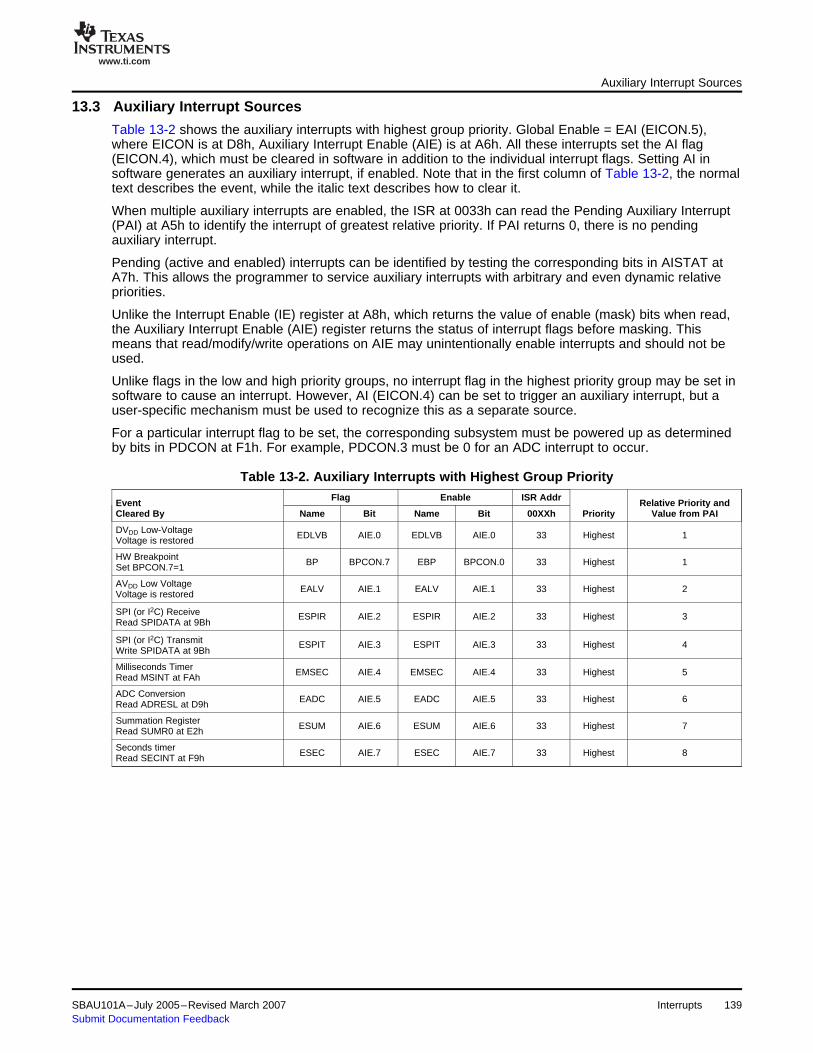
www.ti.com
13.3 Auxiliary Interrupt Sources
Auxiliary Interrupt Sources
Table 13-2 shows the auxiliary interrupts with highest group priority. Global Enable = EAI (EICON.5),where EICON is at D8h, Auxiliary Interrupt Enable (AIE) is at A6h. All these interrupts set the AI flag(EICON.4), which must be cleared in software in addition to the individual interrupt flags. Setting AI insoftware generates an auxiliary interrupt, if enabled. Note that in the first column of Table 13-2, the normaltext describes the event, while the italic text describes how to clear it.
When multiple auxiliary interrupts are enabled, the ISR at 0033h can read the Pending Auxiliary Interrupt(PAI) at A5h to identify the interrupt of greatest relative priority. If PAI returns 0, there is no pendingauxiliary interrupt.
Pending (active and enabled) interrupts can be identified by testing the corresponding bits in AISTAT atA7h. This allows the programmer to service auxiliary interrupts with arbitrary and even dynamic relativepriorities.
Unlike the Interrupt Enable (IE) register at A8h, which returns the value of enable (mask) bits when read,the Auxiliary Interrupt Enable (AIE) register returns the status of interrupt flags before masking. Thismeans that read/modify/write operations on AIE may unintentionally enable interrupts and should not beused.
Unlike flags in the low and high priority groups, no interrupt flag in the highest priority group may be set insoftware to cause an interrupt. However, AI (EICON.4) can be set to trigger an auxiliary interrupt, but auser-specific mechanism must be used to recognize this as a separate source.
For a particular interrupt flag to be set, the corresponding subsystem must be powered up as determinedby bits in PDCON at F1h. For example, PDCON.3 must be 0 for an ADC interrupt to occur.
Table 13-2. Auxiliary Interrupts with Highest Group PriorityFlag Enable ISR Addr
Event Relative Priority andCleared By Name Bit Name Bit 00XXh Priority Value from PAI
DVDD Low-Voltage EDLVB AIE.0 EDLVB AIE.0 33 Highest 1Voltage is restored
HW Breakpoint BP BPCON.7 EBP BPCON.0 33 Highest 1Set BPCON.7=1
AVDD Low Voltage EALV AIE.1 EALV AIE.1 33 Highest 2Voltage is restored
SPI (or I2C) Receive ESPIR AIE.2 ESPIR AIE.2 33 Highest 3Read SPIDATA at 9Bh
SPI (or I2C) Transmit ESPIT AIE.3 ESPIT AIE.3 33 Highest 4Write SPIDATA at 9Bh
Milliseconds Timer EMSEC AIE.4 EMSEC AIE.4 33 Highest 5Read MSINT at FAh
ADC Conversion EADC AIE.5 EADC AIE.5 33 Highest 6Read ADRESL at D9h
Summation Register ESUM AIE.6 ESUM AIE.6 33 Highest 7Read SUMR0 at E2h
Seconds timer ESEC AIE.7 ESEC AIE.7 33 Highest 8Read SECINT at F9h
SBAU101A–July 2005–Revised March 2007 Interrupts 139Submit Documentation Feedback

www.ti.com
13.4 Multiple Interrupts
13.5 Example of Multiple and Nested Interrupts
Multiple Interrupts
In some applications, there may be no interrupts, while in others there may be many. When there is justone interrupt, the ISR is most often relatively easy to write and the model of the timing is simple. However,with multiple sources of different priorities, the complexity, in terms of timing and exact behavior, growsquickly. Since there are three groups of priority (classed as low, high, and highest), it is possible to havethree nested levels of interrupts. For example, the main program may be interrupted by an event of lowpriority, but the ISR may be interrupted by an event of high priority, which in turn could be interrupted byan event of highest priority.
It is essential that there be no unintentional interaction between different interrupts, and that the operatingenvironment or context be restored prior to termination of an ISR. For all but the simplest of ISRs, it isnecessary to save and restore the primary context (PSW and Accumulator) to and from the stack.Similarly, working registers R0 to R7 may need to be PUSHed and POPed, but this process istime-consuming and can be avoided by register bank switching.
Once the primary context has been PUSHed onto the stack, the value of bits 4 and 3 in the PSW may bechanged to select a different bank of 8-bit working registers. In this way, the values in the previous bankare not changed by instructions that reference registers relative to the new bank. It is practical to allocatebank 0 to the main program, bank 1 to low interrupts, bank 2 to high, and bank 3 to highest. Since workingregisters are also mapped to memory locations, it is possible to modify (and corrupt) any register bywriting to an explicit location. For example, R4 of bank 2 is at data address 14h. Care may be needed inthis regard when using multiple interrupts.
Example 13-1 shows ISRs for interrupts of low, high, and highest priority. Based on a clock of11.0592MHz, the program does the following:
1. Toggles signal sync3 (P1.3) as frequently as possible, subject to servicing interrupts. Assuming themain program is implemented as the instruction CPL P1.3, sync3 will toggle every 0.723µs.
2. Transmits a digit between 0 and 3 at 9600 baud on serial port 0 every 20ms, as triggered by themilliseconds system timer.
3. Uses the interrupt from Timer 0 to toggle sync0 (P1.0) every 278µs.4. Uses the interrupt from Timer 2 to toggle sync2 (P1.2) every 10ms.5. Receives characters from serial port 0 via an interrupt and toggles sync1 (P1.1).6. Shows the level of interrupt nesting by the value of the digit transmitted.
If the time to execute the ISR associated with Timer 0 is short, then most interrupts will occur with respectto the main program. However, every application with multiple interrupts should cater to the least likelycombination of events. In this case, it is possible that the main program is interrupted by an overflow fromeither Timer 0 or Timer 2, which is then interrupted due to a character received on serial port 0, whichitself is interrupted by the milliseconds timer. The variable called level will then be 3 and cause a '3' to betransmitted because the MSINT ISR forces a transmit interrupt for serial port 0 by setting TI_0.
The characters most often transmitted are '1' and '2'. However, a '3' may be seen occasionally, dependingupon the relative timing of the received character with respect to the other interrupts. The probability isaffected considerably by the rate at which characters are received, the value of LIMIT, and the efficiencyof the code produced by the compiler.
140 Interrupts SBAU101A–July 2005–Revised March 2007Submit Documentation Feedback
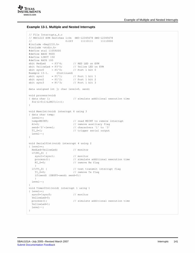
www.ti.com
Example of Multiple and Nested Interrupts
Example 13-1. Multiple and Nested Interrupts
// File Interrupts_4.c// MSC1210 EVM Switches 1:On SW3-12345678 SW6-12345678// 0:Off 11110111 11110000#include <Reg1210.h>#include <stdio.h>#define xtal 11059200#define BAUD 9600#define LIMIT 150#define RATE 100sbit RedLed = P3^4; // RED LED on EVMsbit YellowLed = P3^5; // Yellow LED on EVMsbit sync0 = P1^0; // Port 1 bit 0Example 13-1. (Continued)sbit sync1 = P1^1; // Port 1 bit 1sbit sync2 = P1^2; // Port 1 bit 2sbit sync3 = P1^3; // Port 1 bit 3
data unsigned int j; char level=0, send;
void process(void) data char i; // simulate additional execution timefor(i=0;i<LIMIT;i++);
void MsecInt(void) interrupt 6 using 3 data char temp;level++;temp=MSINT; // read MSINT to remove interruptAI=0; // remove auxiliary flagsend='0'+level; // characters '1' to '3'TI_0=1; // trigger serial outputlevel--;
void Serial0Int(void) interrupt 4 using 2 level++;RedLed=YellowLed; // monitorif(RI_0) sync1=!sync1; // monitorprocess(); // simulate additional execution timeRI_0=0; // remove Rx flag
if(TI_0) // test transmit interrupt flagTI_0=0; // remove Tx flagif(send) SBUF0=send; send=0;
level--;void Timer0Int(void) interrupt 1 using 1 level++;sync0=!sync0; // monitorYellowLed=0;process(); // simulate additional execution timeYellowLed=1;level--;
SBAU101A–July 2005–Revised March 2007 Interrupts 141Submit Documentation Feedback

www.ti.com
Example of Multiple and Nested Interrupts
Example 13-1. Multiple and Nested Interrupts (continued)
void Timer2Int(void) interrupt 5 using 1 level++;sync2=!sync2; // monitorTF2=0; // remove Timer 2 overflow flaglevel--;
void main(void) PDCON=0x7D; // System Timer enabledSCON0=0x50; // Serial 0 enable; RI_0 clearedCKCON=0x20; // Timer 2 at fclk/4; Timers 0 and 1 at fclk/12PCON =0x30; // SMOD = 0 => normal Baud rate equtionTMOD =0x22; // Timers 1 and 0 Auto reloadTCON =0x50; // TR1 and TR0 are 1TH1 =256-xtal/32/12/BAUD; // Timer 1 reload valueTH0 =0; // Overflows every 256 * 12 * tclkT2CON=0x04; // Timer 2 is auto-reload and TR2 is 1RCAP2=65536-xtal/4/RATE;MSEC=xtal/1000 - 1; // 1 ms referenceMSINT=20 - 1; // 20 ms interrupt intervalIP =0x90; // Priorities Timer2 'low', Serial0 'high', Timer0 'low'IE =0xB2; // EA ET2, ES0 and ET0 enabledAIE =0x10; // EMSEC enabledEICON=0x60; // Auxiliary interrupts enabledwhile(1)sync3=!sync3; // foreground program
Interrupts from Timers 0 and 2 are both in the low priority group, and are therefore mutually exclusive andshare register bank 1. The priority of Serial Port 0 is raised to high by writing a '1' to bit 4 of register IP,and therefore uses a different register bank. Similarly, since the milliseconds interrupt is in the highestgroup, the ISR is allocated its own register bank.
If interrupts from Timer 0 and Timer 2 are pending at the same moment, Timer 0 will be serviced firstbecause it has a higher relative priority within the low group.
In this particular example, individual ISRs may not use registers, depending upon the efficiency andoptimization level of the compiler. However, the allocation of register banks ensures mutually exclusivecontexts and is the usual practice.
The interrupt number used in C is given by (ISR Address – 3) divided by 8.
142 Interrupts SBAU101A–July 2005–Revised March 2007Submit Documentation Feedback
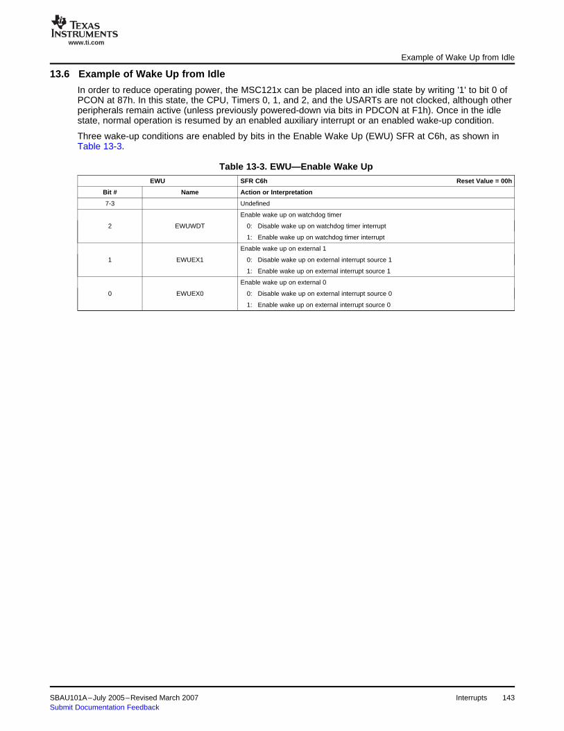
www.ti.com
13.6 Example of Wake Up from Idle
Example of Wake Up from Idle
In order to reduce operating power, the MSC121x can be placed into an idle state by writing '1' to bit 0 ofPCON at 87h. In this state, the CPU, Timers 0, 1, and 2, and the USARTs are not clocked, although otherperipherals remain active (unless previously powered-down via bits in PDCON at F1h). Once in the idlestate, normal operation is resumed by an enabled auxiliary interrupt or an enabled wake-up condition.
Three wake-up conditions are enabled by bits in the Enable Wake Up (EWU) SFR at C6h, as shown inTable 13-3.
Table 13-3. EWU—Enable Wake UpEWU SFR C6h Reset Value = 00h
Bit # Name Action or Interpretation
7-3 Undefined
Enable wake up on watchdog timer
2 EWUWDT 0: Disable wake up on watchdog timer interrupt
1: Enable wake up on watchdog timer interrupt
Enable wake up on external 1
1 EWUEX1 0: Disable wake up on external interrupt source 1
1: Enable wake up on external interrupt source 1
Enable wake up on external 0
0 EWUEX0 0: Disable wake up on external interrupt source 0
1: Enable wake up on external interrupt source 0
SBAU101A–July 2005–Revised March 2007 Interrupts 143Submit Documentation Feedback
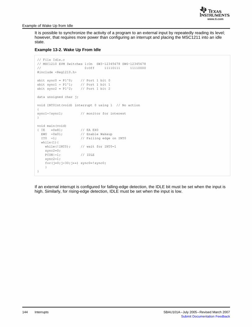
www.ti.com
Example of Wake Up from Idle
It is possible to synchronize the activity of a program to an external input by repeatedly reading its level;however, that requires more power than configuring an interrupt and placing the MSC1211 into an idlestate.
Example 13-2. Wake Up From Idle
// File Idle.c// MSC1210 EVM Switches 1:On SW3-12345678 SW6-12345678// 0:Off 11110111 11110000#include <Reg1210.h>
sbit sync0 = P1^0; // Port 1 bit 0sbit sync1 = P1^1; // Port 1 bit 1sbit sync2 = P1^2; // Port 1 bit 2
data unsigned char j;
void INT0Int(void) interrupt 0 using 1 // No actionsync1=!sync1; // monitor for interest
void main(void) IE =0x81; // EA EX0EWU =0x01; // Enable WakeupIT0 =1; // Falling edge on INT0while(1)while(!INT0); // wait for INT0=1sync2=0;PCON|=1; // IDLEsync2=1;for(j=0;j<30;j++) sync0=!sync0;
If an external interrupt is configured for falling-edge detection, the IDLE bit must be set when the input ishigh. Similarly, for rising-edge detection, IDLE must be set when the input is low.
144 Interrupts SBAU101A–July 2005–Revised March 2007Submit Documentation Feedback

www.ti.com
Revision History
Revision History
Changes from Original (April 2005) to A Revision .......................................................................................................... Page
• Changed document format; updated to new document standard................................................................... 9• Added new Figure 2-2................................................................................................................... 25• Changed format of Table 2-1........................................................................................................... 25• Changed + sign to ± (typo) in ODAC (E6h) description ............................................................................ 37• Changed equation in section 4.5 ...................................................................................................... 48• Added definition to α and β in section 6.3 ............................................................................................ 65• Changed reference from Table 6-3 to Table 6-5 (typo)............................................................................. 72• Changed "?" to "x" (typo) in Table 9-9............................................................................................... 102• Changed "0 1" to "0 or 1" (typo) in bit # 4 port value of Table 10-2 ............................................................. 105• Added fCLK text to 3rd bullet of Section 11.1........................................................................................ 114• Changed Bit 0 text in Table 11-5..................................................................................................... 119• Added new section 11.3.4 and new Table 11-6.................................................................................... 123• Added new section 11.3.6 and new Table 11-8.................................................................................... 123• Changed function text for Modes 1, 2, and 3 in Table 12-2 ...................................................................... 127• Changed 655362 to 65536 (typo) in Table 12-4 ................................................................................... 127• Changed comment text for TI_1=0 in Example 12-1 .............................................................................. 133• Added new Figure 13-1................................................................................................................ 138• Changed list item 3 from 278ms to 278µs in section 13.5........................................................................ 140• Changed "MsecInt" to "MSINT" (typo) in section 13.5 ............................................................................ 140
NOTE: Page numbers for previous revisions may differ from page numbers in the current version.
SBAU101A–July 2005–Revised March 2007 Interrupts 145Submit Documentation Feedback

IMPORTANT NOTICE
Texas Instruments Incorporated and its subsidiaries (TI) reserve the right to make corrections, modifications, enhancements, improvements, and other changes to its products and services at any time and to discontinue any product or service without notice. Customers should obtain the latest relevant information before placing orders and should verify that such information is current and complete. All products are sold subject to TI’s terms and conditions of sale supplied at the time of order acknowledgment. TI warrants performance of its hardware products to the specifications applicable at the time of sale in accordance with TI’s standard warranty. Testing and other quality control techniques are used to the extent TI deems necessary to support this warranty. Except where mandated by government requirements, testing of all parameters of each product is not necessarily performed. TI assumes no liability for applications assistance or customer product design. Customers are responsible for their products and applications using TI components. To minimize the risks associated with customer products and applications, customers should provide adequate design and operating safeguards. TI does not warrant or represent that any license, either express or implied, is granted under any TI patent right, copyright, mask work right, or other TI intellectual property right relating to any combination, machine, or process in which TI products or services are used. Information published by TI regarding third-party products or services does not constitute a license from TI to use such products or services or a warranty or endorsement thereof. Use of such information may require a license from a third party under the patents or other intellectual property of the third party, or a license from TI under the patents or other intellectual property of TI. Reproduction of information in TI data books or data sheets is permissible only if reproduction is without alteration and is accompanied by all associated warranties, conditions, limitations, and notices. Reproduction of this information with alteration is an unfair and deceptive business practice. TI is not responsible or liable for such altered documentation. Resale of TI products or services with statements different from or beyond the parameters stated by TI for that product or service voids all express and any implied warranties for the associated TI product or service and is an unfair and deceptive business practice. TI is not responsible or liable for any such statements. Following are URLs where you can obtain information on other Texas Instruments products and application solutions: Products Applications Amplifiers amplifier.ti.com Audio www.ti.com/audio Data Converters dataconverter.ti.com Automotive www.ti.com/automotive DSP dsp.ti.com Broadband www.ti.com/broadband Interface interface.ti.com Digital Control www.ti.com/digitalcontrol Logic logic.ti.com Military www.ti.com/military Power Mgmt power.ti.com Optical Networking www.ti.com/opticalnetwork Microcontrollers microcontroller.ti.com Security www.ti.com/security Low Power Wireless www.ti.com/lpw Telephony www.ti.com/telephony Video & Imaging www.ti.com/video Wireless www.ti.com/wireless Mailing Address: Texas Instruments Post Office Box 655303 Dallas, Texas 75265
Copyright © 2007, Texas Instruments Incorporated