Embed Size (px)
Citation preview
Lecture 350 – Parallel DACs, Improved Resolution DACs and Serial DACs (3/28/10) Page 350-1
CMOS Analog Circuit Design © P.E. Allen - 2010
LECTURE 350 – PARALLEL DACS, IMPROVED DACRESOLUTION AND SERIAL DACS
LECTURE ORGANIZATIONOutline• Voltage scaling DACs• Charge scaling DACs• Extending the resolution of parallel DACs• Serial DACs• SummaryCMOS Analog Circuit Design, 2nd Edition ReferencePages 626-652
Lecture 350 – Parallel DACs, Improved Resolution DACs and Serial DACs (3/28/10) Page 350-2
CMOS Analog Circuit Design © P.E. Allen - 2010
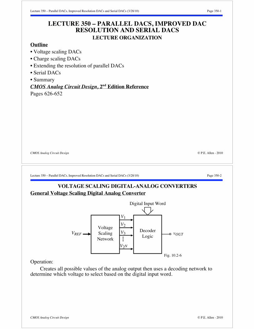
VOLTAGE SCALING DIGITAL-ANALOG CONVERTERSGeneral Voltage Scaling Digital Analog Converter
vOUT
VoltageScalingNetwork
Digital Input Word
VREFDecoder
Logic
V1
V2
V3
V2N
Fig. 10.2-6
Operation:Creates all possible values of the analog output then uses a decoding network to
determine which voltage to select based on the digital input word.
Lecture 350 – Parallel DACs, Improved Resolution DACs and Serial DACs (3/28/10) Page 350-3
CMOS Analog Circuit Design © P.E. Allen - 2010
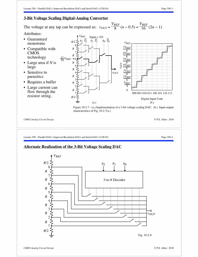
3-Bit Voltage Scaling Digital-Analog Converter
The voltage at any tap can be expressed as: vOUT = VREF
8 (n 0.5) = VREF16 (2n 1)
Attributes:• Guaranteed
monotonic• Compatible with
CMOStechnology
• Large area if N islarge
• Sensitive toparasitics
• Requires a buffer• Large current can
flow through theresistor string.
b2 b1 b0b2 b1 b0
VREF
R/2
R/2
8
7
6
5
4
3
2
1
R
R
R
R
R
R
R
vOUT
000 001 010 011 100 101 110 111
VREF8
2VREF8
3VREF8
4VREF8
5VREF8
6VREF8
7VREF8
VREF
0
Digital Input Code
v OU
T
(a.) (b.)
Figure 10.2-7 - (a.) Implementation of a 3-bit voltage scaling DAC. (b.) Input-output characteristics of Fig. 10.2-7(a.)
1116 VREF
Input = 101
Lecture 350 – Parallel DACs, Improved Resolution DACs and Serial DACs (3/28/10) Page 350-4
CMOS Analog Circuit Design © P.E. Allen - 2010
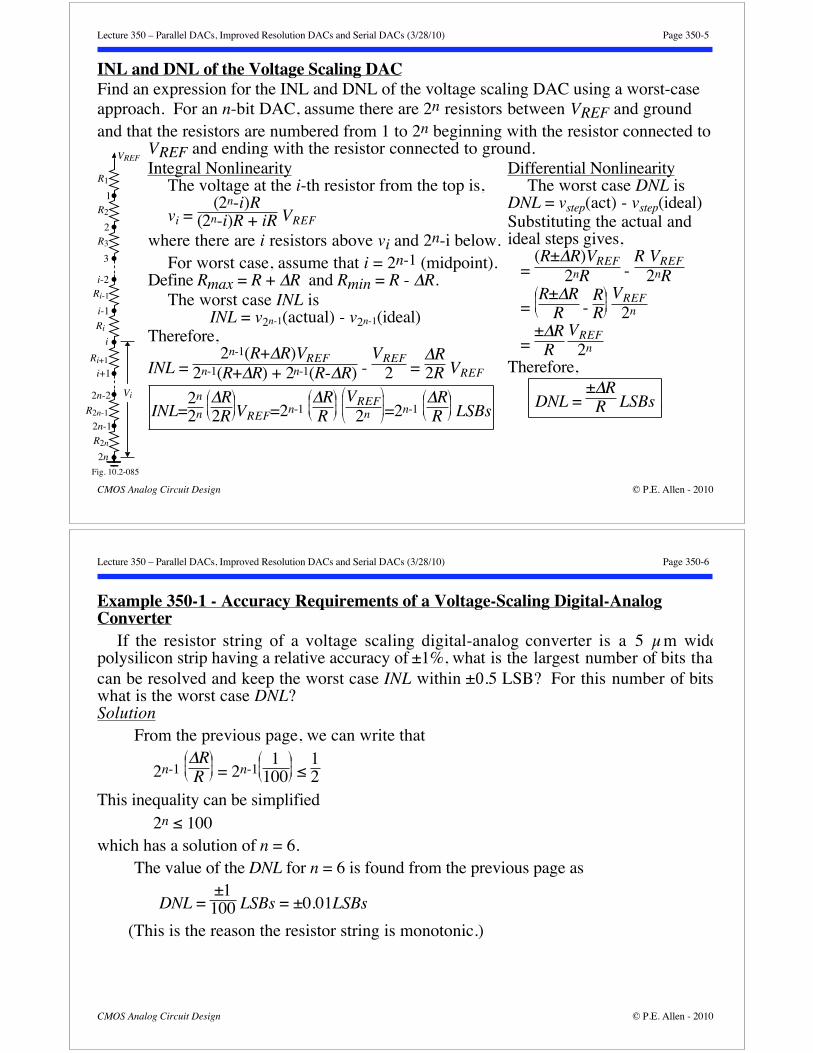
Alternate Realization of the 3-Bit Voltage Scaling DAC
b2 b1 b0
VREF
R/2
R/2
8
7
6
5
4
3
2
1
R
R
R
R
R
R
R
vOUT
3-to-8 Decoder
Fig. 10.2-8
Lecture 350 – Parallel DACs, Improved Resolution DACs and Serial DACs (3/28/10) Page 350-5
CMOS Analog Circuit Design © P.E. Allen - 2010
INL and DNL of the Voltage Scaling DACFind an expression for the INL and DNL of the voltage scaling DAC using a worst-caseapproach. For an n-bit DAC, assume there are 2n resistors between VREF and groundand that the resistors are numbered from 1 to 2n beginning with the resistor connected to
VREF and ending with the resistor connected to ground.Integral Nonlinearity
The voltage at the i-th resistor from the top is,
vi = (2n-i)R
(2n-i)R + iR VREF
where there are i resistors above vi and 2n-i below.For worst case, assume that i = 2n-1 (midpoint).
Define Rmax = R + R and Rmin = R - R.The worst case INL is
INL = v2n-1(actual) - v2n-1(ideal)Therefore,
INL = 2n-1(R+ R)VREF
2n-1(R+ R) + 2n-1(R- R) - VREF
2 = R
2R VREF
INL=2n
2nR
2R VREF=2n-1R
RVREF
2n =2n-1R
R LSBs
Differential NonlinearityThe worst case DNL is
DNL = vstep(act) - vstep(ideal)Substituting the actual andideal steps gives,
= (R± R)VREF
2nR - R VREF
2nR
= R± R
R -RR
VREF2n
= ± R
R VREF
2n Therefore,
DNL =± R
R LSBs
VREF
R1
R2
R3
Ri-1
Ri
Ri+1
R2n
R2n-1
1
2
3
i-2
i-1
i
i+1
2n-2
2n-1
2n
Vi
Fig. 10.2-085
Lecture 350 – Parallel DACs, Improved Resolution DACs and Serial DACs (3/28/10) Page 350-6
CMOS Analog Circuit Design © P.E. Allen - 2010
Example 350-1 - Accuracy Requirements of a Voltage-Scaling Digital-AnalogConverter
If the resistor string of a voltage scaling digital-analog converter is a 5 μm widepolysilicon strip having a relative accuracy of ±1%, what is the largest number of bits thatcan be resolved and keep the worst case INL within ±0.5 LSB? For this number of bitswhat is the worst case DNL?Solution
From the previous page, we can write that
2n-1 R
R = 2n-11
100 12
This inequality can be simplified2n 100
which has a solution of n = 6. The value of the DNL for n = 6 is found from the previous page as
DNL = ±1
100 LSBs = ±0.01LSBs
(This is the reason the resistor string is monotonic.)
Lecture 350 – Parallel DACs, Improved Resolution DACs and Serial DACs (3/28/10) Page 350-7
CMOS Analog Circuit Design © P.E. Allen - 2010
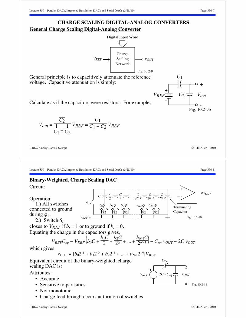
CHARGE SCALING DIGITAL-ANALOG CONVERTERSGeneral Charge Scaling Digital-Analog Converter
vOUT
ChargeScalingNetwork
Digital Input Word
VREF
Fig. 10.2-9
General principle is to capacitively attenuate the referencevoltage. Capacitive attenuation is simply:
Calculate as if the capacitors were resistors. For example,
Vout =
1C2
1C1 +
1C2
VREF = C1
C1 + C2 VREF
C1
C2VREF
+
-
Vout
Fig. 10.2-9b
Lecture 350 – Parallel DACs, Improved Resolution DACs and Serial DACs (3/28/10) Page 350-8
CMOS Analog Circuit Design © P.E. Allen - 2010
Binary-Weighted, Charge Scaling DACCircuit:
Operation:1.) All switches
connected to groundduring 1.
2.) Switch Sicloses to VREF if bi = 1 or to ground if bi = 0.Equating the charge in the capacitors gives,
VREFCeq = VREF b0C +b1C2 +
b2C22 + ... +
bN-1C2N 1 = Ctot vOUT = 2C vOUT
which givesvOUT = [b02-1 + b12-2 + b22-3 + ... + bN-12-N]VREF
Equivalent circuit of the binary-weighted, chargescaling DAC is:Attributes:
• Accurate• Sensitive to parasitics• Not monotonic• Charge feedthrough occurs at turn on of switches
+
-
VREF
φ1
C2 2N-2 2N-1C
4C C C
2N-1C
φ2
S0
φ2 φ2 φ2 φ2
S1 S2 SN-2 SN-1
vOUT
TerminatingCapacitor
Fig. 10.2-10
+
-
VREF
Ceq.
2C - Ceq. vOUT
Fig. 10.2-11
Lecture 350 – Parallel DACs, Improved Resolution DACs and Serial DACs (3/28/10) Page 350-9
CMOS Analog Circuit Design © P.E. Allen - 2010
Integral Nonlinearity of the Charge Scaling DACAgain, we use a worst case approach. Assume an n-bit charge scaling DAC with the
MSB capacitor of C and the LSB capacitor of C/2n-1 and the capacitors have a toleranceof C/C.
The ideal output when the i-th capacitor only is connected to VREF is
vOUT (ideal) = C/2i-1
2C VREF = VREF
2i 2n
2n = 2n
2i LSBs
The maximum and minimum capacitance is Cmax = C + C and Cmin = C - C.Therefore, the actual worst case output for the i-th capacitor is
vOUT(actual) = (C± C)/2i-1
2C VREF = VREF
2i ± C·VREF2iC =
2n
2i ± 2n C2iC LSBs
Now, the INL for the i-th bit is given as
INL(i) = vOUT(actual) - vOUT(ideal) = ±2n C
2iC = 2n-i C
C LSBs
Typically, the worst case value of i occurs for i = 1. Therefore, the worst case INL is
INL = ± 2n-1C
C LSBs
Lecture 350 – Parallel DACs, Improved Resolution DACs and Serial DACs (3/28/10) Page 350-10
CMOS Analog Circuit Design © P.E. Allen - 2010
Differential Nonlinearity of the Charge Scaling DACThe worst case DNL for the binary weighted capacitor array is found when the MSB
changes. The output voltage of the binary weighted capacitor array can be written as
vOUT = Ceq.
(2C-Ceq.) + Ceq. VREF
where Ceq are capacitors whose bits are 1 and (2C - Ceq) are capacitors whose bits are 0.
The worst case DNL can be expressed as
DNL = vstep(worst case)
vstep(ideal) - 1 =
vOUT(1000....) - vOUT(0111....)LSB - 1 LSBs
The worst case choice for the capacitors is to choose C1 larger by C and the remainingcapacitors smaller by C giving,
C1=C+ C, C2 = 12(C- C),...,Cn-1=
12n-2(C- C), Cn=
12n-1(C- C), and Cterm=
12n-1(C- C)
Note that n
Cii=2
+ Cterm = C2+ C3+···+ Cn-1+ Cn+ Cterm = C- C
Lecture 350 – Parallel DACs, Improved Resolution DACs and Serial DACs (3/28/10) Page 350-11
CMOS Analog Circuit Design © P.E. Allen - 2010
Differential Nonlinearity of the Charge Scaling DAC - Continued
vOUT(1000...) = C+ C
(C+ C)+(C- C) VREF = C+ C
2C VREF
= C+ C
2C VREF 2n
2n = 2nC+ C
2C LSBs
and
vOUT(0111...) = (C- C) -Cterm
(C+ C)+(C- C) VREF = (C- C) -
12n-1(C- C)
(C+ C)+(C- C) VREF
= C- C
2C 1 -22n VREF =
2n
2nC- C
2C 1 -22n VREF = 2n
C- C2C 1 -
22n LSBs
vOUT(1000...) - vOUT(0111...)LSB -1 LSBs = 2n
C+ C2C -2n
C- C2C 1-
22n -1 = (2n-1)
CC LSBs
Therefore, DNL = (2n - 1)C
C LSBs
Lecture 350 – Parallel DACs, Improved Resolution DACs and Serial DACs (3/28/10) Page 350-12
CMOS Analog Circuit Design © P.E. Allen - 2010
Example 350-2 - DNL and INL of a Binary Weighted Capacitor Array DACIf the tolerance of the capacitors in an 8-bit, binary weighted, charge scaling DAC are
±0.5%, find the worst case INL and DNL.Solution
For the worst case INL, we get from above thatINL = (27)(±0.005) = ±0.64 LSBs
For the worst case DNL, we can write thatDNL = (28-1)(±0.005) = ±1.275 LSBs
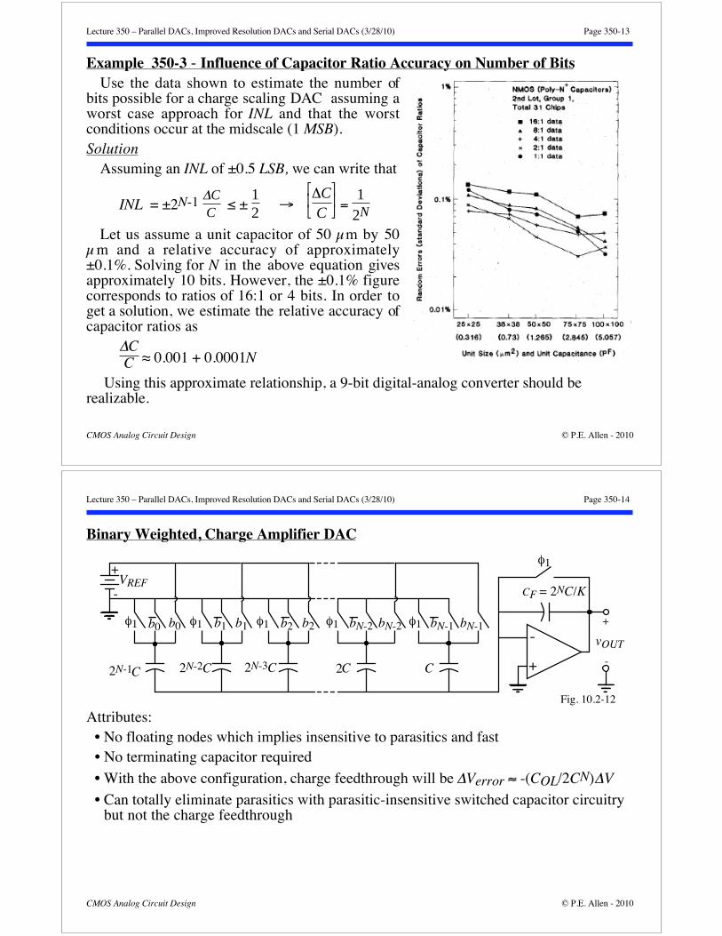
Lecture 350 – Parallel DACs, Improved Resolution DACs and Serial DACs (3/28/10) Page 350-13
CMOS Analog Circuit Design © P.E. Allen - 2010
Example 350-3 - Influence of Capacitor Ratio Accuracy on Number of BitsUse the data shown to estimate the number of
bits possible for a charge scaling DAC assuming aworst case approach for INL and that the worstconditions occur at the midscale (1 MSB).Solution
Assuming an INL of ±0.5 LSB, we can write that
INL = ±2N-1 C
C ±
1
2
C
C =
1
2N
Let us assume a unit capacitor of 50 μm by 50μm and a relative accuracy of approximately±0.1%. Solving for N in the above equation givesapproximately 10 bits. However, the ±0.1% figurecorresponds to ratios of 16:1 or 4 bits. In order toget a solution, we estimate the relative accuracy ofcapacitor ratios as
CC 0.001 + 0.0001N
Using this approximate relationship, a 9-bit digital-analog converter should berealizable.
Lecture 350 – Parallel DACs, Improved Resolution DACs and Serial DACs (3/28/10) Page 350-14
CMOS Analog Circuit Design © P.E. Allen - 2010
Binary Weighted, Charge Amplifier DAC
+
-b0
VREF
2N-1
CF = 2NC/K
+
-
vOUT
C2C
φ1
φ1
+
-
b0 b1φ1 b1 b2φ1 b2 bN-1φ1 bN-1
Fig. 10.2-12
C
bN-2φ1 bN-2
2N-2C 2N-3C
Attributes: • No floating nodes which implies insensitive to parasitics and fast • No terminating capacitor required
• With the above configuration, charge feedthrough will be Verror -(COL/2CN) V
• Can totally eliminate parasitics with parasitic-insensitive switched capacitor circuitrybut not the charge feedthrough
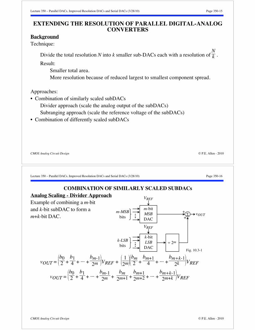
Lecture 350 – Parallel DACs, Improved Resolution DACs and Serial DACs (3/28/10) Page 350-15
CMOS Analog Circuit Design © P.E. Allen - 2010
EXTENDING THE RESOLUTION OF PARALLEL DIGITAL-ANALOGCONVERTERS
BackgroundTechnique:
Divide the total resolution N into k smaller sub-DACs each with a resolution of Nk .
Result:Smaller total area.More resolution because of reduced largest to smallest component spread.
Approaches:• Combination of similarly scaled subDACs
Divider approach (scale the analog output of the subDACs)Subranging approach (scale the reference voltage of the subDACs)
• Combination of differently scaled subDACs
Lecture 350 – Parallel DACs, Improved Resolution DACs and Serial DACs (3/28/10) Page 350-16
CMOS Analog Circuit Design © P.E. Allen - 2010
COMBINATION OF SIMILARLY SCALED SUBDACsAnalog Scaling - Divider ApproachExample of combining a m-bitand k-bit subDAC to form am+k-bit DAC.
vOUT = b02 +
b14 + ··· +
bm-12m VREF +
12m
bm2 +
bm+14 + ··· +
bm+k-12k VREF
vOUT = b02 +
b14 + ··· +
bm-12m +
bm2m+1 +
bm+12m+2 + ··· +
bm+k-12m+k VREF
m-MSBbits
k-LSBbits
m-bitMSBDAC
k-bitLSBDAC
÷ 2m
VREF
VREF
Σ++
vOUT
Fig. 10.3-1
Lecture 350 – Parallel DACs, Improved Resolution DACs and Serial DACs (3/28/10) Page 350-17
CMOS Analog Circuit Design © P.E. Allen - 2010
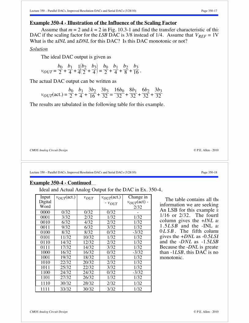
Example 350-4 - Illustration of the Influence of the Scaling FactorAssume that m = 2 and k = 2 in Fig. 10.3-1 and find the transfer characteristic of this
DAC if the scaling factor for the LSB DAC is 3/8 instead of 1/4. Assume that VREF = 1VWhat is the ±INL and ±DNL for this DAC? Is this DAC monotonic or not?
Solution
The ideal DAC output is given as
vOUT = b02 +
b14 +
14
b22 +
b34 =
b02 +
b14 +
b28 +
b316 .
The actual DAC output can be written as
vOUT(act.) = b02 +
b14 +
3b216 +
3b332 =
16b032 +
8b132 +
6b232 +
3b332
The results are tabulated in the following table for this example.
Lecture 350 – Parallel DACs, Improved Resolution DACs and Serial DACs (3/28/10) Page 350-18
CMOS Analog Circuit Design © P.E. Allen - 2010
Example 350-4 - Continued Ideal and Actual Analog Output for the DAC in Ex. 350-4,
The table contains all theinformation we are seekingAn LSB for this example is1/16 or 2/32. The fourthcolumn gives the +INL as1.5LSB and the -INL as0 L S B . The fifth columngives the +DNL as -0.5LSBand the -DNL as -1.5LSBBecause the -DNL is greaterthan -1LSB, this DAC is notmonotonic.
InputDigitalWord
vOUT(act.) vOUT vOUT(act.)- vOUT
Change invOUT(act) -
2/320000 0/32 0/32 0/32 -0001 3/32 2/32 1/32 1/320010 6/32 4/32 2/32 1/320011 9/32 6/32 3/32 1/320100 8/32 8/32 0/32 -3/320101 11/32 10/32 1/32 1/320110 14/32 12/32 2/32 1/320111 17/32 14/32 3/32 1/321000 16/32 16/32 0/32 -3/321001 19/32 18/32 1/32 1/321010 22/32 20/32 2/32 1/321011 25/32 22/32 3/32 1/321100 24/32 24/32 0/32 -3/321101 27/32 26/32 1/32 1/321110 30/32 28/32 2/32 1/32
1111 33/32 30/32 3/32 1/32
Lecture 350 – Parallel DACs, Improved Resolution DACs and Serial DACs (3/28/10) Page 350-19
CMOS Analog Circuit Design © P.E. Allen - 2010
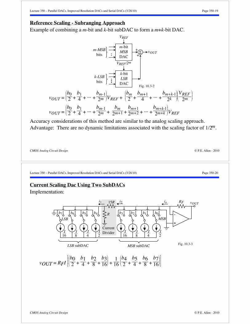
Reference Scaling - Subranging ApproachExample of combining a m-bit and k-bit subDAC to form a m+k-bit DAC.
m-MSBbits
k-LSBbits
m-bitMSBDAC
k-bitLSBDAC
VREF
VREF/2m
Σ++
vOUT
Fig. 10.3-2
vOUT = b02 +
b14 + ··· +
bm-12m VREF +
bm2 +
bm+14 + ··· +
bm+k-12k
VREF2m
vOUT = b02 +
b14 + ··· +
bm-12m +
bm2m+1 +
bm+12m+2 + ··· +
bm+k-12m+k VREF
Accuracy considerations of this method are similar to the analog scaling approach.Advantage: There are no dynamic limitations associated with the scaling factor of 1/2m.
Lecture 350 – Parallel DACs, Improved Resolution DACs and Serial DACs (3/28/10) Page 350-20
CMOS Analog Circuit Design © P.E. Allen - 2010
Current Scaling Dac Using Two SubDACsImplementation:
+
-
I16
I8
I4
I2
I16
I8
I4
I2
15R
RLSB MSB
RF vOUTioi2i1
MSB subDACLSB subDAC
b0b1b2b3b4b5b6b7
CurrentDivider
Fig. 10.3-3
vOUT = RFI b02 +
b14 +
b28 +
b316 +
116
b42 +
b54 +
b68 +
b716
Lecture 350 – Parallel DACs, Improved Resolution DACs and Serial DACs (3/28/10) Page 350-21
CMOS Analog Circuit Design © P.E. Allen - 2010
Charge Scaling DAC Using Two SubDACsImplementation:
+
-
VREF
φ1
C2C
4C
φ2
b7
φ2 φ2 φ2 φ2
b6 b5 b1 b0
vOUT
C
φ2
b48
C8
φ2
b3
φ2
b2
C2C
4CC
8
Cs
Scal
ing
Cap
acito
r
LSB Array MSB ArrayTerminatingCapacitor
070515-01Circuit for LSB Thevenin Eq. Circuit for MSB Thevenin Eq.
Design of the scaling capacitor, Cs:
The series combination of Cs and the LSB array must terminate the MSB array orequal C/8. Therefore, we can write
C8 =
11Cs
+1
2C or
1Cs =
8C -
12C =
162C -
12C =
152C
Lecture 350 – Parallel DACs, Improved Resolution DACs and Serial DACs (3/28/10) Page 350-22
CMOS Analog Circuit Design © P.E. Allen - 2010
Equivalent Circuit of the Charge Scaling Dac Using Two SubDACsSimplified equivalent circuit:
where the Thevenin equivalent voltageof the MSB array is
V1 = 1
15/8 b0 +1/2
15/8 b1 +1/4
15/8 b2 +1/815/8 b3 VREF =
1615
b02 +
b14 +
b28 +
b316 VREF
and the Thevenin equivalent voltage of the LSB array is
V2 = 1/12 b4 +
1/22 b5 +
1/42 b6 +
1/82 b7 VREF =
b42 +
b54 +
b68 +
b816 VREF
Combining the elements of the simplified equivalent circuit above gives
vOUT=
12 +
152
12 +
152 +
815
V1+
815
12 +
152 +
815
V2= 15+15·15
15+15·15+16 V1+16
15+15·15+16 V2= 1516V1+
116V2
vOUT = b02 +
b14 +
b28 +
b316 +
b432 +
b564 +
b6128 +
b7256 VREF =
7
i=0 biVREF
2i+1
+
-
Cs = 2C/15
C + 7C/8 = 15C/8
V1V2
2CvOUT
070515-02
Lecture 350 – Parallel DACs, Improved Resolution DACs and Serial DACs (3/28/10) Page 350-23
CMOS Analog Circuit Design © P.E. Allen - 2010
Charge Amplifier DAC Using Two Binary Weighted Charge Amplifier SubDACsImplementation:
VREF
+
-
vOUT
+
-
C
b4 φ1
b4
C/2
b5 φ1
b5
b6 φ1
b6
b7 φ1
b7
C/4
C/8
+
-2C
φ1
VREF+
-
C
b0 φ1
b0
C/2
b1 φ1
b1
b2 φ1
b2
b3 φ1
b3
C/4
C/8
+
-2C
φ1
C/8
A1 A2
LSB Array MSB Array
vO1
Fig. 10.3-6
Attributes:• MSB subDAC is not dependent upon the accuracy of the scaling factor for the LSB
subDAC.• Insensitive to parasitics, fast• Limited to op amp dynamics (GB)• No ICMR problems with the op amp
Lecture 350 – Parallel DACs, Improved Resolution DACs and Serial DACs (3/28/10) Page 350-24
CMOS Analog Circuit Design © P.E. Allen - 2010
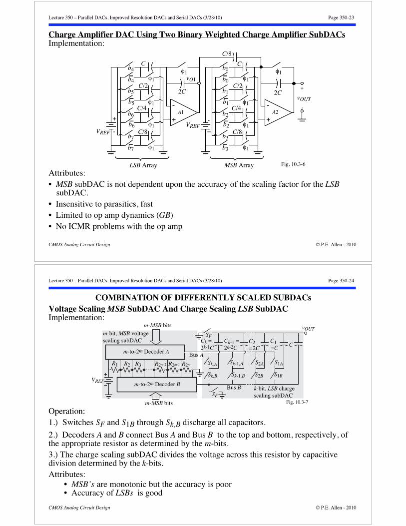
COMBINATION OF DIFFERENTLY SCALED SUBDACsVoltage Scaling MSB SubDAC And Charge Scaling LSB SubDACImplementation:
Ck =2k-1C
Sk-1,A
SF
SF
Bus A
Bus B
Sk,A
Sk,B
Ck-1 =2k-2C
Sk-1,B
C2
=2CC1
=CC
vOUT
S2A
S2B
S1A
S1B
m-to-2m Decoder A
m-to-2m Decoder BVREF
R1 R2 R3 R2m-2 R2m-1 R2m
m-MSB bits
m-MSB bits
m-bit, MSB voltagescaling subDAC
k-bit, LSB chargescaling subDAC
Fig. 10.3-7
Operation:1.) Switches SF and S1B through Sk,B discharge all capacitors.
2.) Decoders A and B connect Bus A and Bus B to the top and bottom, respectively, ofthe appropriate resistor as determined by the m-bits.3.) The charge scaling subDAC divides the voltage across this resistor by capacitivedivision determined by the k-bits.Attributes:
• MSB’s are monotonic but the accuracy is poor• Accuracy of LSBs is good
Lecture 350 – Parallel DACs, Improved Resolution DACs and Serial DACs (3/28/10) Page 350-25
CMOS Analog Circuit Design © P.E. Allen - 2010
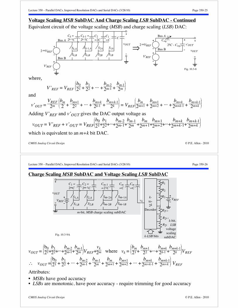
Voltage Scaling MSB SubDAC And Charge Scaling LSB SubDAC - ContinuedEquivalent circuit of the voltage scaling (MSB) and charge scaling (LSB) DAC:
Ck =2k-1C
Sk-1,A
Bus A
Bus B
Sk,A
Sk,B
Ck-1 =2k-2C
Sk,B
C2
=2CC1
=CC
vOUTS2A
S2B
S1A
S1B
2-mVREF
V'REF
2-mVREF
V'REF
vOUT
Ceq.
2kC - Ceq.
Bus A
Bus B
v'OUT
Fig. 10.3-8
where,
V’REF = VREF b021 +
b122 + ··· +
bm-22m-1 +
bm-12m
and
v’OUT = VREF
2m bm2 +
bm+122 + ··· +
bm+k2k-1 +
bm+k-12k = VREF
bm2m+1 +
bm+12m+2 + ··· +
bm+k2m+k-1 +
bm+k-12m+k
Adding V’REF and v’OUT gives the DAC output voltage as
vOUT = V’REF + v’OUT = VREFb021+
b122+···+
bm-22m-1+
bm-12m +
bm2m+1+
bm+12m+2+···+
bm+k2m+k-1+
bm+k-12m+k
which is equivalent to an m+k bit DAC.
Lecture 350 – Parallel DACs, Improved Resolution DACs and Serial DACs (3/28/10) Page 350-26
CMOS Analog Circuit Design © P.E. Allen - 2010
Charge Scaling MSB SubDAC and Voltage Scaling LSB SubDAC
vOUT = b021+
b122+···+
bm-22m-1+
bm-12m VREF+
vk2m where vk =
bm21+
bm+122 +···+
bm+k2k-1 +
bm+k-12k VREF
vOUT =b021 +
b122 + ··· +
bm-22m-1 +
bm-12m +
bm2m+1 +
bm+12m+2 + ··· +
bm+k2m+k-1 +
bm+k-12m+k VREF
Attributes:• MSBs have good accuracy• LSBs are monotonic, have poor accuracy - require trimming for good accuracy
C1 =2mC
S2,AS1,A
S1,B
C2 =2m-1C
S2,B
Cm-1
=21CCm
=CCm=C
vOUTSm-2A
Sm-2B
Sm-1A
Sm-1BVREF
k-to-2k
Decoder
k-LSB bits
R1
R2
R3
R2k-2
R2k-1
R2k
VREF
m-bit, MSB charge scaling subDAC
k-bit,LSB
voltage scaling
subDAC
vk
Fig. 10.3-9A
Lecture 350 – Parallel DACs, Improved Resolution DACs and Serial DACs (3/28/10) Page 350-27
CMOS Analog Circuit Design © P.E. Allen - 2010
Tradeoffs in SubDAC Selection to Enhance Linearity PerformanceAssume a m-bit MSB subDAC and a k-bit LSB subDAC.
MSB Voltage Scaling SubDAC and LSB Charge Scaling SubDAC (n = m+k)INL and DNL of the m-bit MSB voltage-scaling subDAC:
INL(R) = 2m-12n
2m R
R = 2n-1 R
R LSBs and DNL(R) = ± R
R 2n
2m = 2k ± RR LSBs
INL and DNL of the k-bit LSB charge-scaling subDAC:
INL(C) = 2k-1 C
C LSBs and DNL(C) = (2k-1) C
C LSBs
Combining these relationships:
INL = INL(R) + INL(C) = 2n-1R
R + 2k-1C
C LSBs
and DNL = DNL(R) + DNL(C) = 2kR
R + (2k-1)C
C LSBs
MSB Charge Scaling SubDAC and LSB Voltage Scaling SubDAC
INL = INL(R) + INL(C) = 2k-1R
R + 2n-1C
C LSBs
and DNL = DNL(R) + DNL(C) =R
R + (2n-1)C
C LSBs
Lecture 350 – Parallel DACs, Improved Resolution DACs and Serial DACs (3/28/10) Page 350-28
CMOS Analog Circuit Design © P.E. Allen - 2010
Example 350-5 - Design of a DAC using Voltage Scaling for MBSs and ChargeScaling for LSBs
Consider a 12-bit DAC that uses voltage scaling for the MSBs charge scaling for theLSBs. To minimize the capacitor element spread and the number of resistors, choose m =5 and k = 7. Find the tolerances necessary for the resistors and capacitors to give an INLand DNL equal to or less than 2 LSB and 1 LSB, respectively.Solution
Substituting n = 12 and k = 7 into the previous equations gives
2 = 211 R
R + 26 C
C and 1 = 27 R
R + (27-1) C
C
Solving these two equations simultaneously givesC
C = 24-2
211 - 26 - 24 = 0.0071 C
C = 0.71%
RR =
28 - 26 -2218 - 213 - 211 = 0.0008
RR = 0.075%
We see that the capacitor tolerance will be easy to meet but that the resistor tolerancewill require resistor trimming to meet the 0.075% requirement. Because of the 2n-1multiplying R/R in the relationship, we are stuck with approximately 0.075%.Therefore, choose m = 2 (which makes the 0.075% easier to achieve) and let k = 10 whichgives R/R = 0.083% and C/C = 0.12%.
Lecture 350 – Parallel DACs, Improved Resolution DACs and Serial DACs (3/28/10) Page 350-29
CMOS Analog Circuit Design © P.E. Allen - 2010
Example 350-6 - Design of a DAC using Charge Scaling for MBSs and VoltageScaling for LSBs
Consider a 12-bit DAC that uses charge scaling for the MSBs voltage scaling for theLSBs. To minimize the capacitor element spread and the number of resistors, choose m =7 and k = 5. Find the tolerances necessary for the resistors and capacitors to give an INLand DNL equal to or less than 2 LSB and 1 LSB, respectively.Solution
Substituting the values of this example into the relationships developed on a previousslide, we get
2 = 24 R
R + 211 C
C and 1 = R
R + (212-1) C
C
Solving these two equations simultaneously gives
C
C = 24-2
216-211-24 = 0.000221 C
C = 0.0221% and R
R 3
25-1 = 0.0968 R
R = 9.68%
For this example, the resistor tolerance is easy to meet but the capacitor tolerance willbe difficult. To achieve accurate capacitor tolerances, we should decrease the value of mand increase the value of k to achieve a smaller capacitor value spread and therebyenhance the tolerance of the capacitors. If we choose m = 4 and k = 8, the capacitortolerance is 0.049% and the resistor tolerance becomes 0.79% which is still reasonable.The largest to smallest capacitor ratio is 8 rather than 64 which helps to meet thecapacitor tolerance requirements.
Lecture 350 – Parallel DACs, Improved Resolution DACs and Serial DACs (3/28/10) Page 350-30
CMOS Analog Circuit Design © P.E. Allen - 2010
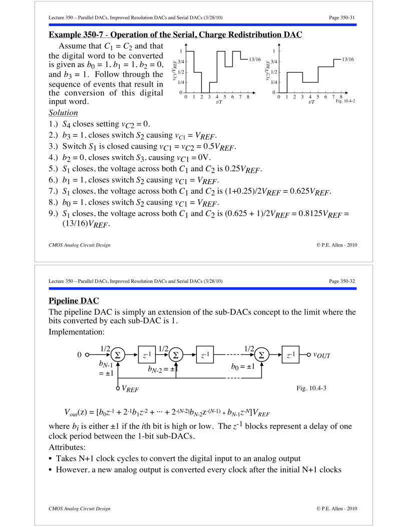
SERIAL DIGITAL-ANALOG CONVERTERSSerial DACs• Typically require one clock pulse to convert one bit• Types considered here are:
Charge-redistributionAlgorithmic
Charge Redistribution DACImplementation:
VREF
S2
S3
S1
S4C2C1 vC2
Fig. 10.4-1Operation:
Switch S1 is the redistribution switch that parallels C1 and C2 sharing their chargeSwitch S2 precharges C1 to VREF if the ith bit, bi, is a 1Switch S3 discharges C1 to zero if the ith bit, bi, is a 0Switch S4 is used at the beginning of the conversion process to initially discharge C2Conversion always begins with the LSB bit and goes to the MSB bit.
Lecture 350 – Parallel DACs, Improved Resolution DACs and Serial DACs (3/28/10) Page 350-31
CMOS Analog Circuit Design © P.E. Allen - 2010
Example 350-7 - Operation of the Serial, Charge Redistribution DACAssume that C1 = C2 and that
the digital word to be convertedis given as b0 = 1, b1 = 1, b2 = 0,and b3 = 1. Follow through thesequence of events that result inthe conversion of this digitalinput word.Solution1.) S4 closes setting vC2 = 0.2.) b3 = 1, closes switch S2 causing vC1 = VREF.3.) Switch S1 is closed causing vC1 = vC2 = 0.5VREF.4.) b2 = 0, closes switch S3, causing vC1 = 0V.5.) S1 closes, the voltage across both C1 and C2 is 0.25VREF.6.) b1 = 1, closes switch S2 causing vC1 = VREF.7.) S1 closes, the voltage across both C1 and C2 is (1+0.25)/2VREF = 0.625VREF.8.) b0 = 1, closes switch S2 causing vC1 = VREF.9.) S1 closes, the voltage across both C1 and C2 is (0.625 + 1)/2VREF = 0.8125VREF =
(13/16)VREF.
0 1 2 3 4 5 6 7 8
1
3/4
1/2
1/4
0
t/T
v C1/
VR
EF
0 1 2 3 4 5 6 7 8
1
3/4
1/2
1/4
0
t/T
v C2/
VR
EF13/16 13/16
Fig. 10.4-2
Lecture 350 – Parallel DACs, Improved Resolution DACs and Serial DACs (3/28/10) Page 350-32
CMOS Analog Circuit Design © P.E. Allen - 2010
Pipeline DACThe pipeline DAC is simply an extension of the sub-DACs concept to the limit where thebits converted by each sub-DAC is 1.Implementation:
Σ z-11/2
bN-1 = ±1
Σ z-11/2
bN-2 = ±1
Σ z-11/2
b0 = ±1
0
VREF
vOUT
Fig. 10.4-3
Vout(z) = [b0z-1 + 2-1b1z-2 + ··· + 2-(N-2)bN-2z-(N-1) + bN-1z-N]VREF
where bi is either ±1 if the ith bit is high or low. The z-1 blocks represent a delay of oneclock period between the 1-bit sub-DACs.Attributes:• Takes N+1 clock cycles to convert the digital input to an analog output• However, a new analog output is converted every clock after the initial N+1 clocks
Lecture 350 – Parallel DACs, Improved Resolution DACs and Serial DACs (3/28/10) Page 350-33
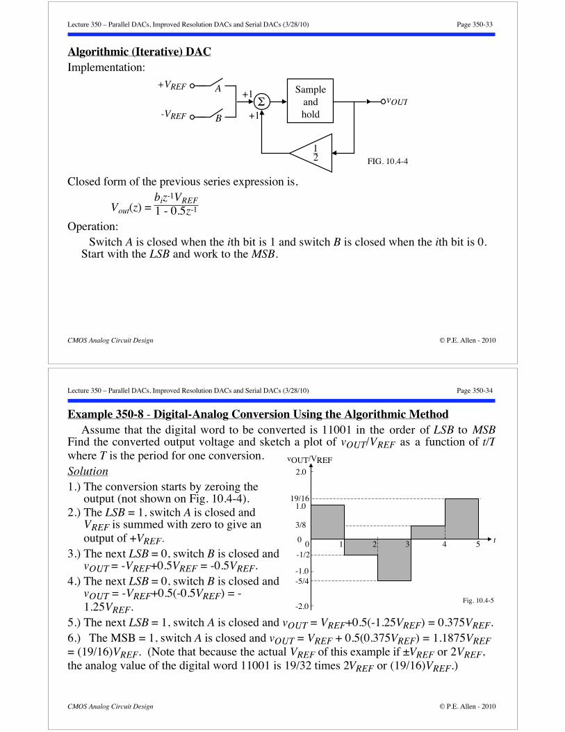
CMOS Analog Circuit Design © P.E. Allen - 2010
Algorithmic (Iterative) DACImplementation:
ΣSample
andhold
+1
+1
12
+VREF A
B-VREF
vOUT
FIG. 10.4-4
Closed form of the previous series expression is,
Vout(z) = biz-1VREF1 - 0.5z-1
Operation:Switch A is closed when the ith bit is 1 and switch B is closed when the ith bit is 0.
Start with the LSB and work to the MSB.
Lecture 350 – Parallel DACs, Improved Resolution DACs and Serial DACs (3/28/10) Page 350-34
CMOS Analog Circuit Design © P.E. Allen - 2010
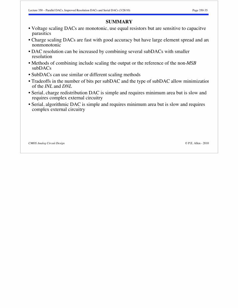
Example 350-8 - Digital-Analog Conversion Using the Algorithmic MethodAssume that the digital word to be converted is 11001 in the order of LSB to MSB
Find the converted output voltage and sketch a plot of vOUT/VREF as a function of t/Twhere T is the period for one conversion.Solution1.) The conversion starts by zeroing the
output (not shown on Fig. 10.4-4).2.) The LSB = 1, switch A is closed and
VREF is summed with zero to give anoutput of +VREF.
3.) The next LSB = 0, switch B is closed andvOUT = -VREF+0.5VREF = -0.5VREF.
4.) The next LSB = 0, switch B is closed andvOUT = -VREF+0.5(-0.5VREF) = -1.25VREF.
5.) The next LSB = 1, switch A is closed and vOUT = VREF+0.5(-1.25VREF) = 0.375VREF.6.) The MSB = 1, switch A is closed and vOUT = VREF + 0.5(0.375VREF) = 1.1875VREF= (19/16)VREF. (Note that because the actual VREF of this example if ±VREF or 2VREF,the analog value of the digital word 11001 is 19/32 times 2VREF or (19/16)VREF.)
0 1 2 3 4 5
2.0
19/161.0
0
-1/2
3/8
-1.0-5/4
-2.0
vOUT/VREF
t
Fig. 10.4-5
Lecture 350 – Parallel DACs, Improved Resolution DACs and Serial DACs (3/28/10) Page 350-35
CMOS Analog Circuit Design © P.E. Allen - 2010
SUMMARY• Voltage scaling DACs are monotonic, use equal resistors but are sensitive to capacitve
parasitics• Charge scaling DACs are fast with good accuracy but have large element spread and are
nonmonotonic• DAC resolution can be increased by combining several subDACs with smaller
resolution• Methods of combining include scaling the output or the reference of the non-MSB
subDACs• SubDACs can use similar or different scaling methods• Tradeoffs in the number of bits per subDAC and the type of subDAC allow minimization
of the INL and DNL• Serial, charge redistribution DAC is simple and requires minimum area but is slow and
requires complex external circuitry• Serial, algorithmic DAC is simple and requires minimum area but is slow and requires
complex external circuitry